EP1772927A1 - Antenna unit and noncontact IC tag - Google Patents
Antenna unit and noncontact IC tag Download PDFInfo
- Publication number
- EP1772927A1 EP1772927A1 EP06254281A EP06254281A EP1772927A1 EP 1772927 A1 EP1772927 A1 EP 1772927A1 EP 06254281 A EP06254281 A EP 06254281A EP 06254281 A EP06254281 A EP 06254281A EP 1772927 A1 EP1772927 A1 EP 1772927A1
- Authority
- EP
- European Patent Office
- Prior art keywords
- antenna
- impedance matching
- tag
- noncontact
- wiring portion
- Prior art date
- Legal status (The legal status is an assumption and is not a legal conclusion. Google has not performed a legal analysis and makes no representation as to the accuracy of the status listed.)
- Granted
Links
Images




Classifications
-
- H—ELECTRICITY
- H01—ELECTRIC ELEMENTS
- H01Q—ANTENNAS, i.e. RADIO AERIALS
- H01Q1/00—Details of, or arrangements associated with, antennas
- H01Q1/12—Supports; Mounting means
- H01Q1/22—Supports; Mounting means by structural association with other equipment or articles
- H01Q1/2208—Supports; Mounting means by structural association with other equipment or articles associated with components used in interrogation type services, i.e. in systems for information exchange between an interrogator/reader and a tag/transponder, e.g. in Radio Frequency Identification [RFID] systems
- H01Q1/2225—Supports; Mounting means by structural association with other equipment or articles associated with components used in interrogation type services, i.e. in systems for information exchange between an interrogator/reader and a tag/transponder, e.g. in Radio Frequency Identification [RFID] systems used in active tags, i.e. provided with its own power source or in passive tags, i.e. deriving power from RF signal
-
- G—PHYSICS
- G06—COMPUTING OR CALCULATING; COUNTING
- G06K—GRAPHICAL DATA READING; PRESENTATION OF DATA; RECORD CARRIERS; HANDLING RECORD CARRIERS
- G06K19/00—Record carriers for use with machines and with at least a part designed to carry digital markings
- G06K19/06—Record carriers for use with machines and with at least a part designed to carry digital markings characterised by the kind of the digital marking, e.g. shape, nature, code
- G06K19/067—Record carriers with conductive marks, printed circuits or semiconductor circuit elements, e.g. credit or identity cards also with resonating or responding marks without active components
- G06K19/07—Record carriers with conductive marks, printed circuits or semiconductor circuit elements, e.g. credit or identity cards also with resonating or responding marks without active components with integrated circuit chips
- G06K19/077—Constructional details, e.g. mounting of circuits in the carrier
- G06K19/07749—Constructional details, e.g. mounting of circuits in the carrier the record carrier being capable of non-contact communication, e.g. constructional details of the antenna of a non-contact smart card
-
- H—ELECTRICITY
- H01—ELECTRIC ELEMENTS
- H01Q—ANTENNAS, i.e. RADIO AERIALS
- H01Q13/00—Waveguide horns or mouths; Slot antennas; Leaky-waveguide antennas; Equivalent structures causing radiation along the transmission path of a guided wave
- H01Q13/08—Radiating ends of two-conductor microwave transmission lines, e.g. of coaxial lines, of microstrip lines
- H01Q13/085—Slot-line radiating ends
-
- H—ELECTRICITY
- H01—ELECTRIC ELEMENTS
- H01Q—ANTENNAS, i.e. RADIO AERIALS
- H01Q13/00—Waveguide horns or mouths; Slot antennas; Leaky-waveguide antennas; Equivalent structures causing radiation along the transmission path of a guided wave
- H01Q13/10—Resonant slot antennas
-
- H—ELECTRICITY
- H10—SEMICONDUCTOR DEVICES; ELECTRIC SOLID-STATE DEVICES NOT OTHERWISE PROVIDED FOR
- H10W—GENERIC PACKAGES, INTERCONNECTIONS, CONNECTORS OR OTHER CONSTRUCTIONAL DETAILS OF DEVICES COVERED BY CLASS H10
- H10W72/00—Interconnections or connectors in packages
- H10W72/071—Connecting or disconnecting
- H10W72/072—Connecting or disconnecting of bump connectors
- H10W72/07251—Connecting or disconnecting of bump connectors characterised by changes in properties of the bump connectors during connecting
-
- H—ELECTRICITY
- H10—SEMICONDUCTOR DEVICES; ELECTRIC SOLID-STATE DEVICES NOT OTHERWISE PROVIDED FOR
- H10W—GENERIC PACKAGES, INTERCONNECTIONS, CONNECTORS OR OTHER CONSTRUCTIONAL DETAILS OF DEVICES COVERED BY CLASS H10
- H10W72/00—Interconnections or connectors in packages
- H10W72/20—Bump connectors, e.g. solder bumps or copper pillars; Dummy bumps; Thermal bumps
Definitions
- the present invention relates to a noncontact IC tag for communication in a noncontact manner using, for example, an electromagnetic wave in a UHF band, and an antenna unit used for the noncontact IC tag.
- Automation has been introduced in various fields by using machines. For example, when automation is tried to be introduced in physical distribution, it is essential that contents of a slip attached to an individual article are machine-readable. As a method of realizing such automation, a barcode label corresponding to contents of an individual slip has been attached to the slip.
- IC in the noncontact IC tag can store individual information of an article as a control object in high capacity. Therefore, an application range is expanded, and for example, the individual information can be used as security information for specifying an individual.
- Figs. 7A to 7B show an example of a noncontact IC tag 101 used in the frequency band of UHF, wherein Fig. 7A shows a plane view, and Fig. 7B shows a front view.
- the noncontact IC tag 101 is configured by an IC chip 111 having a memory function therein, and an antenna 104 provided on a film 103.
- the noncontact IC tag 101 used in the frequency band to increase the read distance, it is necessary that impedance of the IC chip 111 is allowed to match impedance of the antenna 104, the chip and antenna configuring the noncontact IC tag 101, in order to maximize power transmitted and received between the noncontact IC tag 101 and a lead antenna.
- the impedance of the antenna 104 having a shape adapted for a frequency value to be used is allowed to match the impedance of the IC chip 111 determined by an internal component circuit by providing a loading bar 109 parallel to the antenna 104.
- a frequency band that can be used by a noncontact IC tag system is established in various countries to prevent interference with other wireless devices such as a mobile phone.
- the frequency band is different for each country, such as 948 to 956 MHz in Japan, 902 to 928 MHz in the United States, 865 to 868 MHz in Europe, and 918 to 925 MHz in China. Therefore, manufacturers that produce and sell the noncontact IC tag are necessary to design the antenna 104 to be adapted for the frequency in each of the countries, and consequently a difficulty has been given, that is, production or control of the noncontact IC tag 101 becomes extremely complicated.
- UHF band for example, 850 to 960 MHz
- an antenna unit has an antenna and an impedance matching wiring portion, in which when an IC chip is electrically connected to the antenna and the impedance matching wiring portion, a noncontact IC tag is formed, wherein connectable regions are provided in the impedance matching wiring portion, the regions making a direct or indirect connecting position of the IC chip to be adjustable within a predetermined range, so that effective partial length for impedance matching is made adjustable.
- the connectable regions are two ends of the impedance matching wiring portion, and the two ends can be arranged approximately parallel to each other.
- the antenna can be formed in a shape extending in an approximately perpendicular direction to the two ends parallel to each other.
- identification portions for identifying difference in performance due to the connecting positions of the IC chip can be provided near the connectable regions.
- a noncontact IC tag which has the antenna unit, and has the IC chip that is electrically connected to the impedance matching wiring portion and the antenna.
- the antenna unit by which the noncontact IC tag having different resonance frequencies can be easily manufactured, and the noncontact IC tag can be provided.
- Fig. 1A shows a plane view of an RFID (Radio Frequency Identification) tag 1 using the frequency of the UHF band of 850 to 960 MHz
- Fig. 1B shows a front view of the RFID tag 1
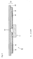
- Fig. 2 shows a vertically sectional front view of an IC module 10.
- the RFID tag 1 is configured by an antenna circuit board 2 having a rectangular sheet shape, and an IC module 10 having an approximately sheet shape in a small rectangle compared with the antenna circuit board 2.
- the antenna circuit board 2 includes a transparent film 3 that is made of PET and has a rectangular shape, and an antenna 4 being slightly smaller than the film 3 is provided on a top of the transparent film 3 by printed wiring. Both of the film 3 and the antenna 4 are sheet members having constant thickness and softness allowing appropriate bendability.
- the antenna 4 is a printed circuit having a cutout portion 5 in a substantially T-shape in the center, and the periphery of the cutout portion 5 is formed as an impedance matching wiring portion (impedance matching circuit) 6.
- impedance matching wiring portion impedance matching circuit
- connecting regions 8, 8 as projecting portions for connection are provided.
- the connecting regions 8, 8 are portions to be two ends for electrically connecting the impedance matching wiring portion 6 to an IC chip 11, and are formed bilaterally symmetric and parallel to each other in a vertically long region shown in Fig. 1A.
- a plurality of marker portions 7 arranged in a back and forth direction are provided near the left connecting region 8. While the marker portions 7, 7 are formed by arranging two holes in the back and forth direction in the embodiment, the holes being cut out from the antenna 4 into a long slit shape in a left and right direction, they are not limited to those, and can be formed in an appropriate configuration, such as a configuration of providing more holes, configuration of providing them near the right connecting region 8, or configuration of providing them near the connecting regions 8, 8 in horizontally two sides respectively.
- the IC module 10 is configured by the IC chip (semiconductor bare chip) 11 and a slap 13.
- the IC chip 11 is a typical IC chip that, for example, has a radio-frequency interface section, control logic section, and storage section within the chip, and operates according to an AC signal, and has a terminal (bump) for combined use of input and output on the top surface as shown in Fig. 2.
- conductive wiring portions 15, 15 are arranged in a horizontally divided manner on a bottom of a film 16 that is made of PET and has a rectangular shape, the portions 15, 15 being printed circuits using aluminum, and a bottom of each conductive wiring portion 15 is covered with an insulating layer 14.
- Each of the insulating layer 14, conductive wiring portion 15, and film 16 is a sheet member having constant thickness and softness allowing appropriate bendability.
- the conductive wiring portions 15, 15 arranged with a certain gap are connected with terminals 12, 12 of the IC chip 11 respectively.
- Connecting ends 19 (see Fig. 1A) of the ICmodule 10 formed in this way have width in the back and forth direction (vertical direction in Fig. 1A), the width being formed sufficiently narrow compared with width in the back and forth direction of the connecting regions 8. Accordingly, a position in the connecting regions 8 to which the IC module 10 is connected can be appropriately adjusted.
- the film 3 is about 32 ⁇ m in thickness
- antenna 4 is about 18 ⁇ m
- IC chip 11 is about 100 ⁇ m
- conductive wiring portion is about 35 ⁇ m
- film 16 is about 18 ⁇ m.
- Size of the RFID tag 1 as a whole that is, size of the film 3 is about 94 mm (left and right direction) by 16 mm (back and forth direction), and the IC module 10 is mounted on the antenna circuit board 2 such that the IC chip 11 is situated in the center in the left and right direction.
- the antenna 4 was formed in the approximately rectangular shape, it may be formed in a shape as shown in a plane view of Fig. 3.
- length L in the left and right direction is 94 mm
- the IC module 10 is mounted such that the IC chip 11 is situated in a central position of the length L (position 47 mm distant from horizontally two ends) .
- the cutout portion 5 is formed in a reverse U-shape, and in corners of the portion 5, corners R1, R4 are round into a circular arc 2 mm in radius, and corners R2, R3 are round into a circular arc 1 mm in radius.
- approximately triangular concave portions 9, 9 are formed symmetrically about a point with respect to a back and forth direction (vertical direction in Fig. 3), and again in corners of the concave portions 9, corners R5, R6 are round into a circular arc 7 mm in radius, and a corner R7 is round into a circular arc 5 mm in radius.
- the RFID tag 1 can transmit and receive data through the electromagnetic wave by the antenna 4, and can store the data in a storage section within the IC chip 11.
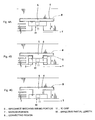
- Figs. 4A to 4C illustrate the mounting positions of the IC module 10 in a case of providing the marker portions 7 in the RFID tag 1 described in conjunction with Figs. 1 and 2.
- Fig. 5 is a table for illustrating change in characteristics in the case that the mounting positions of the IC module 10 is changed as shown in Figs. 4A to 4C using the antenna 4 shown in conjunction with Fig. 3.
- Fig. 4A when the IC module 10 is connected to a side of the impedance matching wiring portion 6 in an X direction shown in the figure, which is a width direction of the antenna 4, such that effective partial length W (circuit length) for impedance matching of the impedance matching wiring portion 6 is shortest (area of the impedance matching wiring portion 6 is smallest), as shown in a position (A) in Fig. 5, an RFID tag 1 having a characteristic value (impedance value, Gain-M value or the like) of which the corresponding frequency is 953 MHz is obtained.
- the IC module 10 points a marker portion 7 nearest to the side of the impedance matching wiring portion 6 among three marker portions 7, consequently it is visible that the frequency corresponds to the marker portion 7.
- Fig. 4C when the IC module 10 is connected to a position further slid (moved in parallel) from the position of Fig. 4B in the X direction shown in the figure, which is a width direction of the antenna 4, the position being at a side opposite to the side of the impedance matching wiring portion 6 (both ends of the impedance matching wiring portion 6), such that the effective partial length W of the impedance matching wiring portion 6 is longest (area of the impedance matching wiring portion 6 is largest), as shown in a position (C) in Fig. 5, an RFID tag 1 having a characteristic value (impedance value, Gain-M value or the like) of which the corresponding frequency is 850 MHz is obtained.
- the IC module 10 points a marker portion 7 at a position most distant from the impedance matching wiring portion 6 among the three marker portions 7, consequently it is visible that the frequency corresponds to the marker portion 7.
- the position of the IC module 10 is changed only by about several millimeters in the X direction respectively in Fig. 4A, Fig. 4B, and Fig. 4C with connection accuracy of about ⁇ 150 ⁇ m.
- the RFID tag 1 even if several types of antennas 4 are not prepared, only by changing the connecting position of the IC module 10 with respect to a single antenna 4, several types of RFID tags 1 having different frequency bands can be manufactured.
- the connecting regions 8, 8 are parallel, the effective partial length of the impedance matching wiring portion 6 can be easily changed by adjusting the mounting positions of the IC module 10.
- the antenna 4 is long in the Y direction perpendicular to the X direction, therefore even if the mounting positions of the IC module 10 are changed, length of the antenna 4 is not changed, consequently the number of parameters varied according to change of the mounting positions of the IC module 10 can be decreased. Accordingly, an RFID tag 1 adapted for a specification of each country can be easily manufactured.
- the marker portions 7 are formed correspondingly to the connecting positions of the IC module 10, a type (country) to which a manufactured RFID tag 1 corresponds can be easily determined at a glance.
- the marker portions 7 can be formed by slit-like holes formed in the antenna 4, that is, can be formed by avoiding printing in the relevant portions during forming printed wiring, cost of the RFID tag 1 is not increased, consequently an antenna circuit board 2 and an RFID tag 1, which have high versatility, can be provided at low cost.
- the IC chip 11 was indirectly connected to the antenna 4 and the impedance matching wiring portion 6 via the conductive wiring portion 15, the IC chip 11 may be directly connected to the antenna 4 and the impedance matching wiring portion 6. Again in this case, the connecting position of the IC chip 11 is adjusted, thereby communication frequency of the RFID tag 1 can be changed.
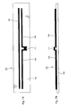
- a marker portion 20 may be formed similarly in the slap 13 as shown in Fig. 6A or Fig. 6B.
- an end of the IC module 10 is acuminated as shown in Fig. 6A, or a hole is formed therein as shown in Fig. 6B, thereby the marker portion 20 can be formed.
- the noncontact IC tag of the embodiment of the invention corresponds to the RFID tag 1 in the above embodiment
- the antenna unit corresponds to the antenna circuit board 2
- the identification portions correspond to the marker portions 7
- the connectable regions and the two ends correspond to the connecting regions 8
- the effective partial length of the impedance matching wiring portion corresponds to the effective partial length W
- the embodiment of the invention is not limited to the configuration of the above embodiment, and may have many embodiments.
Landscapes
- Engineering & Computer Science (AREA)
- Computer Hardware Design (AREA)
- Microelectronics & Electronic Packaging (AREA)
- Physics & Mathematics (AREA)
- General Physics & Mathematics (AREA)
- Theoretical Computer Science (AREA)
- Details Of Aerials (AREA)
- Variable-Direction Aerials And Aerial Arrays (AREA)
Abstract
Description
- The present invention relates to a noncontact IC tag for communication in a noncontact manner using, for example, an electromagnetic wave in a UHF band, and an antenna unit used for the noncontact IC tag.
- Automation has been introduced in various fields by using machines. For example, when automation is tried to be introduced in physical distribution, it is essential that contents of a slip attached to an individual article are machine-readable. As a method of realizing such automation, a barcode label corresponding to contents of an individual slip has been attached to the slip.
- However, to read the barcode label using a so-called barcode reader, a distance between the barcode reader and the barcode label needs to be accurately connected with a direction of the barcode reader directed to the barcode label. Since the connection between the distance and the direction is manually established, much time is taken for read operation, which has obstructed facilitation of the physical distribution. Furthermore, since only a small amount of information can be inputted into the barcode, a region that can be controlled by using the barcode label has been limited to only a narrow region.
- From such background, a noncontact IC tag readable in a noncontact manner using an induction field is currently noted. In the noncontact IC tag, since it communicates in the noncontact manner using the induction field, considerably few restrictions are given on establishing the connection between the distance and the direction in reading stored data compared with the barcode, consequently read operation can be efficiently performed.
- Moreover, IC in the noncontact IC tag can store individual information of an article as a control object in high capacity. Therefore, an application range is expanded, and for example, the individual information can be used as security information for specifying an individual.
- However, types of application using the noncontact IC tag are now increased, and a type of application appears, for which a read distance (about 50 cm) by the induction field is insufficient. As an approach to solve a difficulty on the read distance, a method is begun to be examined, in which a read distance of 3 to 5 m is obtained by using an electromagnetic wave in the UHF band (850 to 950 MHz) or the like (see
JP-A-2004-80600 - Figs. 7A to 7B show an example of a
noncontact IC tag 101 used in the frequency band of UHF, wherein Fig. 7A shows a plane view, and Fig. 7B shows a front view. Thenoncontact IC tag 101 is configured by anIC chip 111 having a memory function therein, and anantenna 104 provided on afilm 103. - Typically, in the
noncontact IC tag 101 used in the frequency band, to increase the read distance, it is necessary that impedance of theIC chip 111 is allowed to match impedance of theantenna 104, the chip and antenna configuring thenoncontact IC tag 101, in order to maximize power transmitted and received between thenoncontact IC tag 101 and a lead antenna. - Therefore, for example, the impedance of the
antenna 104 having a shape adapted for a frequency value to be used is allowed to match the impedance of theIC chip 111 determined by an internal component circuit by providing aloading bar 109 parallel to theantenna 104. - However, in use of the frequency of the UHF band, a frequency band that can be used by a noncontact IC tag system is established in various countries to prevent interference with other wireless devices such as a mobile phone. The frequency band is different for each country, such as 948 to 956 MHz in Japan, 902 to 928 MHz in the United States, 865 to 868 MHz in Europe, and 918 to 925 MHz in China. Therefore, manufacturers that produce and sell the noncontact IC tag are necessary to design the
antenna 104 to be adapted for the frequency in each of the countries, and consequently a difficulty has been given, that is, production or control of thenoncontact IC tag 101 becomes extremely complicated. - It is desirable to provide an antenna unit by which a noncontact IC tag having different resonance frequencies can be easily manufactured in a noncontact IC tag that can communicate through an electromagnetic wave using the UHF band (for example, 850 to 960 MHz) as communication frequency, and provide the noncontact IC tag.
- In an embodiment of the invention, an antenna unit has an antenna and an impedance matching wiring portion, in which when an IC chip is electrically connected to the antenna and the impedance matching wiring portion, a noncontact IC tag is formed, wherein connectable regions are provided in the impedance matching wiring portion, the regions making a direct or indirect connecting position of the IC chip to be adjustable within a predetermined range, so that effective partial length for impedance matching is made adjustable.
- As an aspect of the embodiment of the invention, the connectable regions are two ends of the impedance matching wiring portion, and the two ends can be arranged approximately parallel to each other.
- As another aspect of the embodiment of the invention, the antenna can be formed in a shape extending in an approximately perpendicular direction to the two ends parallel to each other.
- As still another aspect of the embodiment of the invention, identification portions for identifying difference in performance due to the connecting positions of the IC chip can be provided near the connectable regions.
- Moreover, in the embodiment of the invention, a noncontact IC tag can be given, which has the antenna unit, and has the IC chip that is electrically connected to the impedance matching wiring portion and the antenna.
- According to the embodiment of the invention, the antenna unit by which the noncontact IC tag having different resonance frequencies can be easily manufactured, and the noncontact IC tag can be provided.
- IN THE DRAWINGS:
- Figs. 1A to 1B are explanatory views of appearance of an RFID tag;
- Fig. 2 is a vertically sectional front view of an IC module;
- Fig. 3 is a plane view of an antenna in another configuration;
- Figs. 4A to 4C are explanatory views of mounting positions of the IC module;
- Fig. 5 is a table for illustrating change in characteristics of the RFID tag;
- Figs. 6A to 6B are explanatory views of an RFID tag of another embodiment; and
- Figs. 7A to 7B are explanatory views of appearance of a noncontact IC tag in the related art.
- Hereinafter, an embodiment of the invention will be described in conjunction-with drawings.
- Fig. 1A shows a plane view of an RFID (Radio Frequency Identification)
tag 1 using the frequency of the UHF band of 850 to 960 MHz, Fig. 1B shows a front view of theRFID tag 1, and Fig. 2 shows a vertically sectional front view of anIC module 10. - The
RFID tag 1 is configured by anantenna circuit board 2 having a rectangular sheet shape, and anIC module 10 having an approximately sheet shape in a small rectangle compared with theantenna circuit board 2. - The
antenna circuit board 2 includes atransparent film 3 that is made of PET and has a rectangular shape, and anantenna 4 being slightly smaller than thefilm 3 is provided on a top of thetransparent film 3 by printed wiring. Both of thefilm 3 and theantenna 4 are sheet members having constant thickness and softness allowing appropriate bendability. - The
antenna 4 is a printed circuit having acutout portion 5 in a substantially T-shape in the center, and the periphery of thecutout portion 5 is formed as an impedance matching wiring portion (impedance matching circuit) 6. In the left and right of thecutout portion 5, connectingregions regions wiring portion 6 to anIC chip 11, and are formed bilaterally symmetric and parallel to each other in a vertically long region shown in Fig. 1A. On a top of theantenna 4, an insulating layer omitted to be shown is provided. - A plurality of
marker portions 7 arranged in a back and forth direction (vertical direction in Fig. 1A) are provided near the left connectingregion 8. While themarker portions antenna 4 into a long slit shape in a left and right direction, they are not limited to those, and can be formed in an appropriate configuration, such as a configuration of providing more holes, configuration of providing them near the right connectingregion 8, or configuration of providing them near the connectingregions - The
IC module 10 is configured by the IC chip (semiconductor bare chip) 11 and aslap 13. - The
IC chip 11 is a typical IC chip that, for example, has a radio-frequency interface section, control logic section, and storage section within the chip, and operates according to an AC signal, and has a terminal (bump) for combined use of input and output on the top surface as shown in Fig. 2. - In the
slap 13, as shown in Fig. 2,conductive wiring portions film 16 that is made of PET and has a rectangular shape, theportions conductive wiring portion 15 is covered with aninsulating layer 14. Each of theinsulating layer 14,conductive wiring portion 15, andfilm 16 is a sheet member having constant thickness and softness allowing appropriate bendability. - The
conductive wiring portions terminals IC chip 11 respectively. - Connecting ends 19 (see Fig. 1A) of the
ICmodule 10 formed in this way have width in the back and forth direction (vertical direction in Fig. 1A), the width being formed sufficiently narrow compared with width in the back and forth direction of the connectingregions 8. Accordingly, a position in the connectingregions 8 to which theIC module 10 is connected can be appropriately adjusted. - To explain thickness of respective members, the
film 3 is about 32 µm in thickness,antenna 4 is about 18 µm,IC chip 11 is about 100 µm, conductive wiring portion is about 35 µm, andfilm 16 is about 18 µm. - Size of the
RFID tag 1 as a whole, that is, size of thefilm 3 is about 94 mm (left and right direction) by 16 mm (back and forth direction), and theIC module 10 is mounted on theantenna circuit board 2 such that theIC chip 11 is situated in the center in the left and right direction. - While the
antenna 4 was formed in the approximately rectangular shape, it may be formed in a shape as shown in a plane view of Fig. 3. In theantenna 4, length L in the left and right direction is 94 mm, and theIC module 10 is mounted such that theIC chip 11 is situated in a central position of the length L (position 47 mm distant from horizontally two ends) . Thecutout portion 5 is formed in a reverse U-shape, and in corners of theportion 5, corners R1, R4 are round into acircular arc 2 mm in radius, and corners R2, R3 are round into acircular arc 1 mm in radius. - In horizontally halfway portions of the
antenna 4, approximately triangularconcave portions concave portions 9, corners R5, R6 are round into acircular arc 7 mm in radius, and a corner R7 is round into acircular arc 5 mm in radius. - According to a configuration as above, the
RFID tag 1 can transmit and receive data through the electromagnetic wave by theantenna 4, and can store the data in a storage section within theIC chip 11. - Next, the mounting positions of the
IC module 10 with respect to the connectingregions 8, and difference in characteristics of theRFID tag 1 due to the positions are described. - Figs. 4A to 4C illustrate the mounting positions of the
IC module 10 in a case of providing themarker portions 7 in theRFID tag 1 described in conjunction with Figs. 1 and 2. - Fig. 5 is a table for illustrating change in characteristics in the case that the mounting positions of the
IC module 10 is changed as shown in Figs. 4A to 4C using theantenna 4 shown in conjunction with Fig. 3. - First, as shown in Fig. 4A, when the
IC module 10 is connected to a side of the impedancematching wiring portion 6 in an X direction shown in the figure, which is a width direction of theantenna 4, such that effective partial length W (circuit length) for impedance matching of the impedancematching wiring portion 6 is shortest (area of the impedancematching wiring portion 6 is smallest), as shown in a position (A) in Fig. 5, anRFID tag 1 having a characteristic value (impedance value, Gain-M value or the like) of which the corresponding frequency is 953 MHz is obtained. At that time, theIC module 10 points amarker portion 7 nearest to the side of the impedancematching wiring portion 6 among threemarker portions 7, consequently it is visible that the frequency corresponds to themarker portion 7. - Next, as shown in Fig. 4B, when the
IC module 10 is connected to a position slid (moved in parallel) from the position of Fig. 4A in the X direction shown in the figure, which is the width direction of theantenna 4, such that the effective partial length W of the impedancematching wiring portion 6 is about medium, the position being an about central position of the connectingregion 8, as shown in a position (B) in Fig. 5, anRFID tag 1 having a characteristic value (impedance value, Gain-M value or the like) of which the corresponding frequency is 915 MHz is obtained. - Next, as shown in Fig. 4C, when the
IC module 10 is connected to a position further slid (moved in parallel) from the position of Fig. 4B in the X direction shown in the figure, which is a width direction of theantenna 4, the position being at a side opposite to the side of the impedance matching wiring portion 6 (both ends of the impedance matching wiring portion 6), such that the effective partial length W of the impedancematching wiring portion 6 is longest (area of the impedancematching wiring portion 6 is largest), as shown in a position (C) in Fig. 5, anRFID tag 1 having a characteristic value (impedance value, Gain-M value or the like) of which the corresponding frequency is 850 MHz is obtained. At that time, theIC module 10 points amarker portion 7 at a position most distant from the impedancematching wiring portion 6 among the threemarker portions 7, consequently it is visible that the frequency corresponds to themarker portion 7. - In the embodiment, the position of the
IC module 10 is changed only by about several millimeters in the X direction respectively in Fig. 4A, Fig. 4B, and Fig. 4C with connection accuracy of about ±150 µm. - As described hereinbefore, according to the
RFID tag 1, even if several types ofantennas 4 are not prepared, only by changing the connecting position of theIC module 10 with respect to asingle antenna 4, several types ofRFID tags 1 having different frequency bands can be manufactured. - Since the connecting
regions matching wiring portion 6 can be easily changed by adjusting the mounting positions of theIC module 10. - Compared with a direction in which the mounting positions of the
IC module 10 can be changed, or the X direction in Fig. 4, theantenna 4 is long in the Y direction perpendicular to the X direction, therefore even if the mounting positions of theIC module 10 are changed, length of theantenna 4 is not changed, consequently the number of parameters varied according to change of the mounting positions of theIC module 10 can be decreased. Accordingly, anRFID tag 1 adapted for a specification of each country can be easily manufactured. - Moreover, since the
marker portions 7 are formed correspondingly to the connecting positions of theIC module 10, a type (country) to which a manufacturedRFID tag 1 corresponds can be easily determined at a glance. - In addition, since the
marker portions 7 can be formed by slit-like holes formed in theantenna 4, that is, can be formed by avoiding printing in the relevant portions during forming printed wiring, cost of theRFID tag 1 is not increased, consequently anantenna circuit board 2 and anRFID tag 1, which have high versatility, can be provided at low cost. - While the
IC chip 11 was indirectly connected to theantenna 4 and the impedancematching wiring portion 6 via theconductive wiring portion 15, theIC chip 11 may be directly connected to theantenna 4 and the impedancematching wiring portion 6. Again in this case, the connecting position of theIC chip 11 is adjusted, thereby communication frequency of theRFID tag 1 can be changed. - While the
slap 13 of theIC module 10 was formed in a rectangular shape, amarker portion 20 may be formed similarly in theslap 13 as shown in Fig. 6A or Fig. 6B. In this case, an end of theIC module 10 is acuminated as shown in Fig. 6A, or a hole is formed therein as shown in Fig. 6B, thereby themarker portion 20 can be formed. - In this case, even if the connecting position of the
IC module 10 is changed in a small area, amarker portion 7 pointed by theIC module 10 can be more clearly seen. - In correspondence relationship between a configuration of an embodiment of the invention and the above embodiment, the noncontact IC tag of the embodiment of the invention corresponds to the
RFID tag 1 in the above embodiment, and similarly, the antenna unit corresponds to theantenna circuit board 2, the identification portions correspond to themarker portions 7, the connectable regions and the two ends correspond to the connectingregions 8, and the effective partial length of the impedance matching wiring portion corresponds to the effective partial length W, however, the embodiment of the invention is not limited to the configuration of the above embodiment, and may have many embodiments.
Claims (5)
- An antenna unit characterized by comprising an antenna and an impedance matching wiring portion, in which when an IC chip is electrically connected to the antenna and the impedance matching wiring portion, a noncontact IC tag is formed,
wherein connectable regions are provided in the impedance matching wiring portion, the regions making a direct or indirect connecting position of the IC chip to be adjustable within a predetermined range, so that effective partial length for impedance matching is made adjustable. - The antenna unit according to claim 1:
wherein the connectable regions are two ends of the impedance matching wiring portion, and the two ends are arranged approximately parallel to each other. - The antenna unit according to claim 2:
wherein the antenna is formed in a shape extending in an approximately perpendicular direction to the two ends parallel to each other. - The antenna unit according to claim 1, 2, or 3:
wherein identification portions for identifying difference in performance due to connecting positions of the IC chip are provided near the connectable regions. - A noncontact IC tag having the antenna unit according to any one of claims 1 to 4:
wherein an IC chip is electrically connected to the impedance matching wiring portion and the antenna.
Applications Claiming Priority (1)
| Application Number | Priority Date | Filing Date | Title |
|---|---|---|---|
| JP2005283676A JP4075919B2 (en) | 2005-09-29 | 2005-09-29 | Antenna unit and non-contact IC tag |
Publications (2)
| Publication Number | Publication Date |
|---|---|
| EP1772927A1 true EP1772927A1 (en) | 2007-04-11 |
| EP1772927B1 EP1772927B1 (en) | 2016-12-14 |
Family
ID=37770924
Family Applications (1)
| Application Number | Title | Priority Date | Filing Date |
|---|---|---|---|
| EP06254281.6A Expired - Lifetime EP1772927B1 (en) | 2005-09-29 | 2006-08-15 | Antenna unit and noncontact IC tag |
Country Status (5)
| Country | Link |
|---|---|
| US (1) | US7963451B2 (en) |
| EP (1) | EP1772927B1 (en) |
| JP (1) | JP4075919B2 (en) |
| CN (1) | CN1941498A (en) |
| TW (1) | TWI337325B (en) |
Cited By (6)
| Publication number | Priority date | Publication date | Assignee | Title |
|---|---|---|---|---|
| WO2009011376A1 (en) | 2007-07-18 | 2009-01-22 | Murata Manufacturing Co., Ltd. | Wireless ic device |
| EP2166490A4 (en) * | 2007-07-17 | 2010-11-17 | Murata Manufacturing Co | WIRELESS IC DEVICE AND ELECTRONIC APPARATUS |
| EP2357705A4 (en) * | 2008-11-14 | 2013-08-14 | Toppan Printing Co Ltd | CONTACTLESS IC LABEL |
| US8960557B2 (en) | 2008-05-21 | 2015-02-24 | Murata Manufacturing Co., Ltd. | Wireless IC device |
| EP2928015A1 (en) * | 2007-07-18 | 2015-10-07 | Murata Manufacturing Co., Ltd. | Radio frequency ic device and electronic apparatus |
| EP2928021A1 (en) * | 2007-07-04 | 2015-10-07 | Murata Manufacturing Co., Ltd. | Wireless ic device and component for wireless ic device |
Families Citing this family (100)
| Publication number | Priority date | Publication date | Assignee | Title |
|---|---|---|---|---|
| US8220717B2 (en) * | 2006-01-05 | 2012-07-17 | Hitachi Chemical Co., Ltd. | Tubular container enabling individual identification |
| US7519328B2 (en) | 2006-01-19 | 2009-04-14 | Murata Manufacturing Co., Ltd. | Wireless IC device and component for wireless IC device |
| JP4135770B2 (en) | 2006-04-14 | 2008-08-20 | 株式会社村田製作所 | antenna |
| US9064198B2 (en) | 2006-04-26 | 2015-06-23 | Murata Manufacturing Co., Ltd. | Electromagnetic-coupling-module-attached article |
| JP4281850B2 (en) | 2006-06-30 | 2009-06-17 | 株式会社村田製作所 | optical disk |
| JP4718434B2 (en) * | 2006-08-16 | 2011-07-06 | 富士通株式会社 | Electronics |
| JP4775442B2 (en) | 2006-09-26 | 2011-09-21 | 株式会社村田製作所 | Article with electromagnetic coupling module |
| JP2008092198A (en) * | 2006-09-29 | 2008-04-17 | Renesas Technology Corp | Rfid label tag, and its manufacturing method |
| JP5027481B2 (en) * | 2006-11-06 | 2012-09-19 | 株式会社日立製作所 | IC tag |
| JP4950627B2 (en) * | 2006-11-10 | 2012-06-13 | 株式会社日立製作所 | RFIC tag and its use |
| JP4888494B2 (en) | 2007-02-06 | 2012-02-29 | 株式会社村田製作所 | Packaging material with electromagnetic coupling module |
| EP2133827B1 (en) | 2007-04-06 | 2012-04-25 | Murata Manufacturing Co. Ltd. | Radio ic device |
| JP4697332B2 (en) | 2007-04-09 | 2011-06-08 | 株式会社村田製作所 | Wireless IC device |
| US8235299B2 (en) | 2007-07-04 | 2012-08-07 | Murata Manufacturing Co., Ltd. | Wireless IC device and component for wireless IC device |
| EP2138962B1 (en) * | 2007-04-26 | 2012-01-04 | Murata Manufacturing Co. Ltd. | Wireless ic device |
| WO2008136257A1 (en) | 2007-04-27 | 2008-11-13 | Murata Manufacturing Co., Ltd. | Wireless ic device |
| JP4666101B2 (en) | 2007-04-27 | 2011-04-06 | 株式会社村田製作所 | Wireless IC device |
| WO2008140037A1 (en) | 2007-05-11 | 2008-11-20 | Murata Manufacturing Co., Ltd. | Wireless ic device |
| CN101542831B (en) | 2007-07-09 | 2014-06-25 | 株式会社村田制作所 | Wireless ic device |
| JP5034736B2 (en) * | 2007-07-17 | 2012-09-26 | 株式会社村田製作所 | Wireless IC device |
| JP5104865B2 (en) | 2007-07-18 | 2012-12-19 | 株式会社村田製作所 | Wireless IC device |
| US20090021352A1 (en) | 2007-07-18 | 2009-01-22 | Murata Manufacturing Co., Ltd. | Radio frequency ic device and electronic apparatus |
| JP4434311B2 (en) | 2007-07-18 | 2010-03-17 | 株式会社村田製作所 | Wireless IC device and manufacturing method thereof |
| EP2096709B1 (en) | 2007-12-20 | 2012-04-25 | Murata Manufacturing Co., Ltd. | Radio ic device |
| EP2557528A3 (en) | 2007-12-26 | 2017-01-18 | Murata Manufacturing Co., Ltd. | Antenna device and wireless IC device |
| JP5267463B2 (en) | 2008-03-03 | 2013-08-21 | 株式会社村田製作所 | Wireless IC device and wireless communication system |
| JP4518211B2 (en) | 2008-03-03 | 2010-08-04 | 株式会社村田製作所 | Compound antenna |
| JP5169329B2 (en) * | 2008-03-06 | 2013-03-27 | 東レ株式会社 | Planar antenna |
| JP4404166B2 (en) | 2008-03-26 | 2010-01-27 | 株式会社村田製作所 | Wireless IC device |
| JP4535209B2 (en) | 2008-04-14 | 2010-09-01 | 株式会社村田製作所 | Wireless IC device, electronic apparatus, and method for adjusting resonance frequency of wireless IC device |
| CN102007644B (en) * | 2008-04-24 | 2013-10-16 | 东丽株式会社 | Non-contact IC tag |
| WO2009142068A1 (en) | 2008-05-22 | 2009-11-26 | 株式会社村田製作所 | Wireless ic device and method for manufacturing the same |
| CN102047271B (en) | 2008-05-26 | 2014-12-17 | 株式会社村田制作所 | Wireless IC device system and authenticity judgment method of wireless IC device |
| EP3509162A1 (en) | 2008-05-28 | 2019-07-10 | Murata Manufacturing Co., Ltd. | Wireless ic device and component for a wireless ic device |
| JP4557186B2 (en) | 2008-06-25 | 2010-10-06 | 株式会社村田製作所 | Wireless IC device and manufacturing method thereof |
| EP2306586B1 (en) | 2008-07-04 | 2014-04-02 | Murata Manufacturing Co. Ltd. | Wireless ic device |
| EP2320519B1 (en) | 2008-08-19 | 2017-04-12 | Murata Manufacturing Co., Ltd. | Wireless ic device and method for manufacturing same |
| JPWO2010038813A1 (en) * | 2008-09-30 | 2012-03-01 | ニッタ株式会社 | Wireless communication improving sheet body, wireless communication IC tag, wireless communication IC tag manufacturing method, information transmission medium, and wireless communication system |
| WO2010047214A1 (en) | 2008-10-24 | 2010-04-29 | 株式会社村田製作所 | Radio ic device |
| JP4525869B2 (en) | 2008-10-29 | 2010-08-18 | 株式会社村田製作所 | Wireless IC device |
| WO2010055945A1 (en) | 2008-11-17 | 2010-05-20 | 株式会社村田製作所 | Antenna and wireless ic device |
| CN102273012B (en) | 2009-01-09 | 2013-11-20 | 株式会社村田制作所 | Wireless IC device and wireless IC module |
| JP5041077B2 (en) | 2009-01-16 | 2012-10-03 | 株式会社村田製作所 | High frequency device and wireless IC device |
| EP2385580B1 (en) | 2009-01-30 | 2014-04-09 | Murata Manufacturing Co., Ltd. | Antenna and wireless ic device |
| JP5510450B2 (en) | 2009-04-14 | 2014-06-04 | 株式会社村田製作所 | Wireless IC device |
| EP2568417B1 (en) | 2009-04-21 | 2018-07-04 | Murata Manufacturing Co., Ltd. | Antenna device and method of setting resonant frequency of antenna device |
| JP5447515B2 (en) | 2009-06-03 | 2014-03-19 | 株式会社村田製作所 | Wireless IC device and manufacturing method thereof |
| JP5516580B2 (en) | 2009-06-19 | 2014-06-11 | 株式会社村田製作所 | Wireless IC device and method for coupling power feeding circuit and radiation plate |
| JP5182431B2 (en) | 2009-09-28 | 2013-04-17 | 株式会社村田製作所 | Wireless IC device and environmental state detection method using the same |
| CN102577646B (en) | 2009-09-30 | 2015-03-04 | 株式会社村田制作所 | Circuit substrate and method of manufacture thereof |
| JP5304580B2 (en) | 2009-10-02 | 2013-10-02 | 株式会社村田製作所 | Wireless IC device |
| WO2011045970A1 (en) | 2009-10-16 | 2011-04-21 | 株式会社村田製作所 | Antenna and wireless ic device |
| JP5418600B2 (en) | 2009-10-27 | 2014-02-19 | 株式会社村田製作所 | Transceiver and RFID tag reader |
| CN102576930A (en) | 2009-11-04 | 2012-07-11 | 株式会社村田制作所 | Communication terminal and information processing system |
| EP2498207B1 (en) | 2009-11-04 | 2014-12-31 | Murata Manufacturing Co., Ltd. | Wireless ic tag, reader/writer, and information processing system |
| WO2011055703A1 (en) | 2009-11-04 | 2011-05-12 | 株式会社村田製作所 | Communication terminal and information processing system |
| CN104617374B (en) | 2009-11-20 | 2018-04-06 | 株式会社村田制作所 | Mobile communication terminal |
| TWI446269B (en) * | 2009-12-03 | 2014-07-21 | 財團法人工業技術研究院 | Wireless communication device |
| WO2011077877A1 (en) | 2009-12-24 | 2011-06-30 | 株式会社村田製作所 | Antenna and handheld terminal |
| US8061624B2 (en) * | 2009-12-28 | 2011-11-22 | Avery Dennison Corporation | RFID strap and cutting device |
| CN102782937B (en) | 2010-03-03 | 2016-02-17 | 株式会社村田制作所 | Wireless communication devices and wireless communication terminal |
| JP5652470B2 (en) | 2010-03-03 | 2015-01-14 | 株式会社村田製作所 | Wireless communication module and wireless communication device |
| WO2011111509A1 (en) | 2010-03-12 | 2011-09-15 | 株式会社村田製作所 | Radio communication device and metallic article |
| WO2011118379A1 (en) | 2010-03-24 | 2011-09-29 | 株式会社村田製作所 | Rfid system |
| JP5630499B2 (en) | 2010-03-31 | 2014-11-26 | 株式会社村田製作所 | Antenna apparatus and wireless communication device |
| JP5170156B2 (en) | 2010-05-14 | 2013-03-27 | 株式会社村田製作所 | Wireless IC device |
| JP5299351B2 (en) | 2010-05-14 | 2013-09-25 | 株式会社村田製作所 | Wireless IC device |
| WO2012005278A1 (en) | 2010-07-08 | 2012-01-12 | 株式会社村田製作所 | Antenna and rfid device |
| CN102859790B (en) | 2010-07-28 | 2015-04-01 | 株式会社村田制作所 | Antenna device and communication terminal equipment |
| JP5423897B2 (en) | 2010-08-10 | 2014-02-19 | 株式会社村田製作所 | Printed wiring board and wireless communication system |
| JP5234071B2 (en) | 2010-09-03 | 2013-07-10 | 株式会社村田製作所 | RFIC module |
| JP5630506B2 (en) | 2010-09-30 | 2014-11-26 | 株式会社村田製作所 | Wireless IC device |
| JP5758909B2 (en) | 2010-10-12 | 2015-08-05 | 株式会社村田製作所 | Communication terminal device |
| WO2012053412A1 (en) | 2010-10-21 | 2012-04-26 | 株式会社村田製作所 | Communication terminal device |
| US20120104103A1 (en) * | 2010-10-29 | 2012-05-03 | Nxp B.V. | Integrated pcb uhf rfid matching network/antenna |
| US9299021B2 (en) * | 2010-11-11 | 2016-03-29 | Avery Dennison Corporation | RFID devices and methods for manufacturing |
| US10381720B2 (en) | 2010-12-08 | 2019-08-13 | Nxp B.V. | Radio frequency identification (RFID) integrated circuit (IC) and matching network/antenna embedded in surface mount devices (SMD) |
| CN105048058B (en) | 2011-01-05 | 2017-10-27 | 株式会社村田制作所 | Wireless communication devices |
| CN103299325B (en) | 2011-01-14 | 2016-03-02 | 株式会社村田制作所 | RFID chip packaging and RFID tags |
| DE202011002173U1 (en) * | 2011-02-01 | 2011-06-01 | ASTRA Gesellschaft für Asset Management mbH & Co. KG, 30890 | detection microchip |
| JP5370616B2 (en) | 2011-02-28 | 2013-12-18 | 株式会社村田製作所 | Wireless communication device |
| JP5630566B2 (en) | 2011-03-08 | 2014-11-26 | 株式会社村田製作所 | Antenna device and communication terminal device |
| KR101317226B1 (en) | 2011-04-05 | 2013-10-15 | 가부시키가이샤 무라타 세이사쿠쇼 | Wireless communication device |
| WO2012141070A1 (en) | 2011-04-13 | 2012-10-18 | 株式会社村田製作所 | Wireless ic device and wireless communication terminal |
| WO2012157596A1 (en) | 2011-05-16 | 2012-11-22 | 株式会社村田製作所 | Wireless ic device |
| KR101338173B1 (en) | 2011-07-14 | 2013-12-06 | 가부시키가이샤 무라타 세이사쿠쇼 | Wireless communication device |
| CN103370886B (en) | 2011-07-15 | 2015-05-20 | 株式会社村田制作所 | Wireless communication device |
| JP5660217B2 (en) | 2011-07-19 | 2015-01-28 | 株式会社村田製作所 | Antenna device, RFID tag, and communication terminal device |
| JP5418737B2 (en) | 2011-09-09 | 2014-02-19 | 株式会社村田製作所 | Antenna apparatus and wireless device |
| JP5874075B2 (en) * | 2011-11-16 | 2016-03-01 | 北川工業株式会社 | Non-contact IC tag |
| JP5344108B1 (en) | 2011-12-01 | 2013-11-20 | 株式会社村田製作所 | Wireless IC device and manufacturing method thereof |
| TWI469444B (en) * | 2011-12-28 | 2015-01-11 | Taiwan Lamination Ind Inc | Packaging material with T - slot antenna |
| WO2013115019A1 (en) | 2012-01-30 | 2013-08-08 | 株式会社村田製作所 | Wireless ic device |
| JP5464307B2 (en) | 2012-02-24 | 2014-04-09 | 株式会社村田製作所 | ANTENNA DEVICE AND WIRELESS COMMUNICATION DEVICE |
| JP5886100B2 (en) * | 2012-03-23 | 2016-03-16 | ニッタ株式会社 | Wireless IC tag |
| CN104487985B (en) | 2012-04-13 | 2020-06-26 | 株式会社村田制作所 | RFID tag inspection method and inspection device |
| US11514288B2 (en) * | 2014-08-10 | 2022-11-29 | Amatech Group Limited | Contactless metal card constructions |
| CN107437648B (en) * | 2016-05-28 | 2021-04-20 | 富泰华工业(深圳)有限公司 | Multi-feed UHF RFID Tag Antenna |
| JP6658607B2 (en) | 2017-02-22 | 2020-03-04 | オムロン株式会社 | Product manufacturing method, exterior parts and antenna pattern selection device |
| USD981380S1 (en) * | 2021-06-25 | 2023-03-21 | Xerafy Inc. | Set of RFID antenna and protective cover |
Citations (3)
| Publication number | Priority date | Publication date | Assignee | Title |
|---|---|---|---|---|
| US20020003496A1 (en) * | 2000-06-01 | 2002-01-10 | Brady Michael John | Adjustable length antenna system for RF transponders |
| WO2003009007A2 (en) * | 2001-07-19 | 2003-01-30 | 3M Innovative Properties Company | Rfid tag with bridge circuit assembly and methods of use |
| EP1686649A1 (en) * | 2005-02-01 | 2006-08-02 | Fujitsu Limited | A meander line antenna |
Family Cites Families (5)
| Publication number | Priority date | Publication date | Assignee | Title |
|---|---|---|---|---|
| US6483473B1 (en) * | 2000-07-18 | 2002-11-19 | Marconi Communications Inc. | Wireless communication device and method |
| JP4789348B2 (en) | 2001-05-31 | 2011-10-12 | リンテック株式会社 | Planar coil component, method for adjusting characteristic of planar coil component, ID tag, and method for adjusting resonance frequency of ID tag |
| US7336243B2 (en) * | 2003-05-29 | 2008-02-26 | Sky Cross, Inc. | Radio frequency identification tag |
| JP2005204179A (en) | 2004-01-16 | 2005-07-28 | Tdk Corp | Module substrate with antenna, and radio module using the same |
| JP2005259153A (en) | 2005-03-25 | 2005-09-22 | Mitsubishi Materials Corp | Structure of antenna coil of RFID transponder and method of adjusting resonance frequency using the antenna coil |
-
2005
- 2005-09-29 JP JP2005283676A patent/JP4075919B2/en not_active Expired - Fee Related
-
2006
- 2006-08-10 US US11/501,825 patent/US7963451B2/en active Active
- 2006-08-15 EP EP06254281.6A patent/EP1772927B1/en not_active Expired - Lifetime
- 2006-09-05 CN CNA2006101281277A patent/CN1941498A/en active Pending
- 2006-09-13 TW TW095133912A patent/TWI337325B/en not_active IP Right Cessation
Patent Citations (3)
| Publication number | Priority date | Publication date | Assignee | Title |
|---|---|---|---|---|
| US20020003496A1 (en) * | 2000-06-01 | 2002-01-10 | Brady Michael John | Adjustable length antenna system for RF transponders |
| WO2003009007A2 (en) * | 2001-07-19 | 2003-01-30 | 3M Innovative Properties Company | Rfid tag with bridge circuit assembly and methods of use |
| EP1686649A1 (en) * | 2005-02-01 | 2006-08-02 | Fujitsu Limited | A meander line antenna |
Cited By (11)
| Publication number | Priority date | Publication date | Assignee | Title |
|---|---|---|---|---|
| EP2928021A1 (en) * | 2007-07-04 | 2015-10-07 | Murata Manufacturing Co., Ltd. | Wireless ic device and component for wireless ic device |
| EP2166618B1 (en) * | 2007-07-04 | 2016-11-16 | Murata Manufacturing Co., Ltd. | Radio ic device and component for radio ic device |
| EP2343779B1 (en) * | 2007-07-04 | 2018-05-09 | Murata Manufacturing Co., Ltd. | Wireless ic device and component for wireless ic device |
| EP2166490A4 (en) * | 2007-07-17 | 2010-11-17 | Murata Manufacturing Co | WIRELESS IC DEVICE AND ELECTRONIC APPARATUS |
| US7997501B2 (en) | 2007-07-17 | 2011-08-16 | Murata Manufacturing Co., Ltd. | Wireless IC device and electronic apparatus |
| WO2009011376A1 (en) | 2007-07-18 | 2009-01-22 | Murata Manufacturing Co., Ltd. | Wireless ic device |
| EP2086052A4 (en) * | 2007-07-18 | 2010-08-11 | Murata Manufacturing Co | INTEGRATED CIRCUIT WIRELESS DEVICE |
| CN101578736B (en) * | 2007-07-18 | 2013-02-27 | 株式会社村田制作所 | Wireless ic device |
| EP2928015A1 (en) * | 2007-07-18 | 2015-10-07 | Murata Manufacturing Co., Ltd. | Radio frequency ic device and electronic apparatus |
| US8960557B2 (en) | 2008-05-21 | 2015-02-24 | Murata Manufacturing Co., Ltd. | Wireless IC device |
| EP2357705A4 (en) * | 2008-11-14 | 2013-08-14 | Toppan Printing Co Ltd | CONTACTLESS IC LABEL |
Also Published As
| Publication number | Publication date |
|---|---|
| US7963451B2 (en) | 2011-06-21 |
| JP4075919B2 (en) | 2008-04-16 |
| TW200713071A (en) | 2007-04-01 |
| EP1772927B1 (en) | 2016-12-14 |
| JP2007096768A (en) | 2007-04-12 |
| CN1941498A (en) | 2007-04-04 |
| TWI337325B (en) | 2011-02-11 |
| US20070069037A1 (en) | 2007-03-29 |
Similar Documents
| Publication | Publication Date | Title |
|---|---|---|
| US7963451B2 (en) | Antenna unit and noncontact IC tag | |
| EP1641140B1 (en) | Data communication device | |
| US8774712B2 (en) | Contactless communication medium, antenna pattern-placed medium, communication apparatus, and antenna adjusting method | |
| TWI474553B (en) | Antenna and transporter | |
| KR101012528B1 (en) | RFID tag | |
| US7323977B2 (en) | Tunable RFID tag for global applications | |
| KR101041329B1 (en) | 2 frequency common antenna device | |
| US10552724B2 (en) | RFID tag and article having RFID tag attached thereto | |
| EP3550731B1 (en) | Nfc antenna in a mobile device | |
| US20110128125A1 (en) | Antenna device and system including antenna device | |
| JP2007150642A (en) | Interrogator for wireless tag, antenna for wireless tag, wireless tag system, and wireless tag selector | |
| US9865913B2 (en) | Communication terminal and card antenna module | |
| JP2005244778A (en) | Small antenna and wireless tag provided with the same | |
| JP5223584B2 (en) | Wireless communication device | |
| US20140184461A1 (en) | Antenna Assembly | |
| JP2005165703A (en) | Non-contact identification medium | |
| CN211655071U (en) | Card type radio communication apparatus | |
| EP1851822B1 (en) | Transponder tuning method and a transponder | |
| KR100820544B1 (en) | RDF tag and its antenna | |
| EP2138962B1 (en) | Wireless ic device | |
| KR20230031574A (en) | Shield can having antenna function and electronic module including the same | |
| JP4218044B2 (en) | 3D antenna | |
| CN114730364A (en) | RFID tag | |
| CN113748431A (en) | RFID tag and antenna | |
| JP4873158B2 (en) | RFID reader device |
Legal Events
| Date | Code | Title | Description |
|---|---|---|---|
| PUAI | Public reference made under article 153(3) epc to a published international application that has entered the european phase |
Free format text: ORIGINAL CODE: 0009012 |
|
| AK | Designated contracting states |
Kind code of ref document: A1 Designated state(s): AT BE BG CH CY CZ DE DK EE ES FI FR GB GR HU IE IS IT LI LT LU LV MC NL PL PT RO SE SI SK TR |
|
| AX | Request for extension of the european patent |
Extension state: AL BA HR MK YU |
|
| 17P | Request for examination filed |
Effective date: 20070529 |
|
| 17Q | First examination report despatched |
Effective date: 20070702 |
|
| AKX | Designation fees paid |
Designated state(s): DE FI FR GB IT |
|
| REG | Reference to a national code |
Ref country code: DE Ref legal event code: R079 Ref document number: 602006051207 Country of ref document: DE Free format text: PREVIOUS MAIN CLASS: H01Q0005020000 Ipc: H01Q0005500000 |
|
| RIC1 | Information provided on ipc code assigned before grant |
Ipc: G06K 19/077 20060101ALN20160601BHEP Ipc: H01Q 13/10 20060101ALN20160601BHEP Ipc: H01Q 1/38 20060101ALN20160601BHEP Ipc: H01Q 5/50 20150101AFI20160601BHEP |
|
| GRAP | Despatch of communication of intention to grant a patent |
Free format text: ORIGINAL CODE: EPIDOSNIGR1 |
|
| INTG | Intention to grant announced |
Effective date: 20160729 |
|
| RIN1 | Information on inventor provided before grant (corrected) |
Inventor name: KAWAI, WAKAHIRO |
|
| GRAS | Grant fee paid |
Free format text: ORIGINAL CODE: EPIDOSNIGR3 |
|
| GRAA | (expected) grant |
Free format text: ORIGINAL CODE: 0009210 |
|
| AK | Designated contracting states |
Kind code of ref document: B1 Designated state(s): DE FI FR GB IT |
|
| REG | Reference to a national code |
Ref country code: GB Ref legal event code: FG4D |
|
| REG | Reference to a national code |
Ref country code: DE Ref legal event code: R096 Ref document number: 602006051207 Country of ref document: DE |
|
| PG25 | Lapsed in a contracting state [announced via postgrant information from national office to epo] |
Ref country code: FI Free format text: LAPSE BECAUSE OF FAILURE TO SUBMIT A TRANSLATION OF THE DESCRIPTION OR TO PAY THE FEE WITHIN THE PRESCRIBED TIME-LIMIT Effective date: 20161214 |
|
| PG25 | Lapsed in a contracting state [announced via postgrant information from national office to epo] |
Ref country code: IT Free format text: LAPSE BECAUSE OF FAILURE TO SUBMIT A TRANSLATION OF THE DESCRIPTION OR TO PAY THE FEE WITHIN THE PRESCRIBED TIME-LIMIT Effective date: 20161214 |
|
| REG | Reference to a national code |
Ref country code: DE Ref legal event code: R097 Ref document number: 602006051207 Country of ref document: DE |
|
| PLBE | No opposition filed within time limit |
Free format text: ORIGINAL CODE: 0009261 |
|
| STAA | Information on the status of an ep patent application or granted ep patent |
Free format text: STATUS: NO OPPOSITION FILED WITHIN TIME LIMIT |
|
| 26N | No opposition filed |
Effective date: 20170915 |
|
| GBPC | Gb: european patent ceased through non-payment of renewal fee |
Effective date: 20170815 |
|
| REG | Reference to a national code |
Ref country code: FR Ref legal event code: ST Effective date: 20180430 |
|
| PG25 | Lapsed in a contracting state [announced via postgrant information from national office to epo] |
Ref country code: GB Free format text: LAPSE BECAUSE OF NON-PAYMENT OF DUE FEES Effective date: 20170815 |
|
| PG25 | Lapsed in a contracting state [announced via postgrant information from national office to epo] |
Ref country code: FR Free format text: LAPSE BECAUSE OF NON-PAYMENT OF DUE FEES Effective date: 20170831 |
|
| PGFP | Annual fee paid to national office [announced via postgrant information from national office to epo] |
Ref country code: DE Payment date: 20240819 Year of fee payment: 19 |
|
| REG | Reference to a national code |
Ref country code: DE Ref legal event code: R119 Ref document number: 602006051207 Country of ref document: DE |
|
| PG25 | Lapsed in a contracting state [announced via postgrant information from national office to epo] |
Ref country code: DE Free format text: LAPSE BECAUSE OF NON-PAYMENT OF DUE FEES Effective date: 20260303 |