EP1772908A2 - Wafer level image module, method for making the same and apparatus for assembling and testing the same - Google Patents
Wafer level image module, method for making the same and apparatus for assembling and testing the same Download PDFInfo
- Publication number
- EP1772908A2 EP1772908A2 EP06020946A EP06020946A EP1772908A2 EP 1772908 A2 EP1772908 A2 EP 1772908A2 EP 06020946 A EP06020946 A EP 06020946A EP 06020946 A EP06020946 A EP 06020946A EP 1772908 A2 EP1772908 A2 EP 1772908A2
- Authority
- EP
- European Patent Office
- Prior art keywords
- photo sensor
- wafer level
- level image
- lens set
- image module
- Prior art date
- Legal status (The legal status is an assumption and is not a legal conclusion. Google has not performed a legal analysis and makes no representation as to the accuracy of the status listed.)
- Granted
Links
Images


Classifications
-
- H—ELECTRICITY
- H10—SEMICONDUCTOR DEVICES; ELECTRIC SOLID-STATE DEVICES NOT OTHERWISE PROVIDED FOR
- H10F—INORGANIC SEMICONDUCTOR DEVICES SENSITIVE TO INFRARED RADIATION, LIGHT, ELECTROMAGNETIC RADIATION OF SHORTER WAVELENGTH OR CORPUSCULAR RADIATION
- H10F39/00—Integrated devices, or assemblies of multiple devices, comprising at least one element covered by group H10F30/00, e.g. radiation detectors comprising photodiode arrays
- H10F39/80—Constructional details of image sensors
- H10F39/806—Optical elements or arrangements associated with the image sensors
- H10F39/8063—Microlenses
-
- H—ELECTRICITY
- H04—ELECTRIC COMMUNICATION TECHNIQUE
- H04N—PICTORIAL COMMUNICATION, e.g. TELEVISION
- H04N23/00—Cameras or camera modules comprising electronic image sensors; Control thereof
- H04N23/57—Mechanical or electrical details of cameras or camera modules specially adapted for being embedded in other devices
-
- H—ELECTRICITY
- H10—SEMICONDUCTOR DEVICES; ELECTRIC SOLID-STATE DEVICES NOT OTHERWISE PROVIDED FOR
- H10F—INORGANIC SEMICONDUCTOR DEVICES SENSITIVE TO INFRARED RADIATION, LIGHT, ELECTROMAGNETIC RADIATION OF SHORTER WAVELENGTH OR CORPUSCULAR RADIATION
- H10F39/00—Integrated devices, or assemblies of multiple devices, comprising at least one element covered by group H10F30/00, e.g. radiation detectors comprising photodiode arrays
- H10F39/80—Constructional details of image sensors
- H10F39/804—Containers or encapsulations
-
- H—ELECTRICITY
- H10—SEMICONDUCTOR DEVICES; ELECTRIC SOLID-STATE DEVICES NOT OTHERWISE PROVIDED FOR
- H10F—INORGANIC SEMICONDUCTOR DEVICES SENSITIVE TO INFRARED RADIATION, LIGHT, ELECTROMAGNETIC RADIATION OF SHORTER WAVELENGTH OR CORPUSCULAR RADIATION
- H10F39/00—Integrated devices, or assemblies of multiple devices, comprising at least one element covered by group H10F30/00, e.g. radiation detectors comprising photodiode arrays
- H10F39/80—Constructional details of image sensors
- H10F39/806—Optical elements or arrangements associated with the image sensors
-
- H—ELECTRICITY
- H10—SEMICONDUCTOR DEVICES; ELECTRIC SOLID-STATE DEVICES NOT OTHERWISE PROVIDED FOR
- H10F—INORGANIC SEMICONDUCTOR DEVICES SENSITIVE TO INFRARED RADIATION, LIGHT, ELECTROMAGNETIC RADIATION OF SHORTER WAVELENGTH OR CORPUSCULAR RADIATION
- H10F77/00—Constructional details of devices covered by this subclass
- H10F77/40—Optical elements or arrangements
- H10F77/407—Optical elements or arrangements indirectly associated with the devices
-
- H—ELECTRICITY
- H04—ELECTRIC COMMUNICATION TECHNIQUE
- H04N—PICTORIAL COMMUNICATION, e.g. TELEVISION
- H04N17/00—Diagnosis, testing or measuring for television systems or their details
- H04N17/002—Diagnosis, testing or measuring for television systems or their details for television cameras
-
- H—ELECTRICITY
- H10—SEMICONDUCTOR DEVICES; ELECTRIC SOLID-STATE DEVICES NOT OTHERWISE PROVIDED FOR
- H10F—INORGANIC SEMICONDUCTOR DEVICES SENSITIVE TO INFRARED RADIATION, LIGHT, ELECTROMAGNETIC RADIATION OF SHORTER WAVELENGTH OR CORPUSCULAR RADIATION
- H10F39/00—Integrated devices, or assemblies of multiple devices, comprising at least one element covered by group H10F30/00, e.g. radiation detectors comprising photodiode arrays
- H10F39/011—Manufacture or treatment of image sensors covered by group H10F39/12
- H10F39/026—Wafer-level processing
-
- H—ELECTRICITY
- H10—SEMICONDUCTOR DEVICES; ELECTRIC SOLID-STATE DEVICES NOT OTHERWISE PROVIDED FOR
- H10W—GENERIC PACKAGES, INTERCONNECTIONS, CONNECTORS OR OTHER CONSTRUCTIONAL DETAILS OF DEVICES COVERED BY CLASS H10
- H10W72/00—Interconnections or connectors in packages
- H10W72/851—Dispositions of multiple connectors or interconnections
- H10W72/874—On different surfaces
- H10W72/884—Die-attach connectors and bond wires
-
- H—ELECTRICITY
- H10—SEMICONDUCTOR DEVICES; ELECTRIC SOLID-STATE DEVICES NOT OTHERWISE PROVIDED FOR
- H10W—GENERIC PACKAGES, INTERCONNECTIONS, CONNECTORS OR OTHER CONSTRUCTIONAL DETAILS OF DEVICES COVERED BY CLASS H10
- H10W90/00—Package configurations
- H10W90/701—Package configurations characterised by the relative positions of pads or connectors relative to package parts
- H10W90/731—Package configurations characterised by the relative positions of pads or connectors relative to package parts of die-attach connectors
- H10W90/734—Package configurations characterised by the relative positions of pads or connectors relative to package parts of die-attach connectors between a chip and a stacked insulating package substrate, interposer or RDL
-
- H—ELECTRICITY
- H10—SEMICONDUCTOR DEVICES; ELECTRIC SOLID-STATE DEVICES NOT OTHERWISE PROVIDED FOR
- H10W—GENERIC PACKAGES, INTERCONNECTIONS, CONNECTORS OR OTHER CONSTRUCTIONAL DETAILS OF DEVICES COVERED BY CLASS H10
- H10W90/00—Package configurations
- H10W90/701—Package configurations characterised by the relative positions of pads or connectors relative to package parts
- H10W90/751—Package configurations characterised by the relative positions of pads or connectors relative to package parts of bond wires
- H10W90/754—Package configurations characterised by the relative positions of pads or connectors relative to package parts of bond wires between a chip and a stacked insulating package substrate, interposer or RDL
Definitions
- the present invention relates to image modules and more particularly, to a wafer level image module, the method for making the same and the apparatus for assembling and testing the same.
- FIG. 12 shows a conventional CMOS (Complementary Metal-Oxide Semiconductor) image module 80.
- the CMOS image module 80 comprises a sensor chip 82 and a lens holder 81 covering the sensor chip 82.
- the lens holder 81 comprises a rotary lens barrel 83, and a lens set 84 on the center of the rotary lens barrel 83.
- the lens set 84 is mapping an image onto the sensor chip 82
- the rotary lens barrel 83 is rotatable to change the distance between the lens set 84 and the sensor chip 82, thereby focusing light rays on the sensor chip 82.
- FIG. 13 shows an image module according to WO2004/027880 .
- This design of image module comprises an image pickup device 103 and a set of lenses 111 and 127.
- the lenses 111 and 127 are arranged in a stack and closely attached to the image pickup device 103 to map the image of incident light rays onto the image pickup device 103.
- the main feature of this patent is that the image pickup device 103 and the lenses 111 and 127 are made through an integrated circuit manufacturing process to minimize the size for use in a cell phone, PDA, or any of a variety of other consumer electronics.
- the lenses 111 and 127 may deform by the manufacturing process and the manufacturing temperature.
- the focal distance of the finished product shows a 0-50 ⁇ m error when compared to the original theoretical design.
- the lenses 111 and 127 cannot accurately focus the image of incident light rays onto the image pickup device 103, resulting in an out-of-focus problem (see the imaginary line A or B in FIG 13).
- the respective size tolerance for example, 0-20 ⁇ m thickness tolerance of each glass chip makes distance control between the lenses 111 and 127 and the image pickup device 103 difficult, resulting in inaccurate focusing of the lenses 111 and 127 on the image pickup device 103.
- the present invention has been accomplished under the circumstances in view. It is an objective of the present invention to provide a wafer level image sensor, which has adjustment means to compensate focus offset, thereby improving the image mapping quality.
- the wafer level image module comprises a photo sensor, a lens set, and an adjustment member.
- the photo sensor outputs an electrical signal when induced by light.
- the lens set maps the image of incident light rays onto the photo sensor.
- the adjustment member is set between the photo sensor and the lens set to control the distance between the photo sensor and the lens sent, and to compensate the focus offset of the photo sensor, enabling the lens set to accurately focus the image of incident light rays onto the photo sensor.
- the method for making a wafer level image module comprises the steps of a) providing a photo sensor, b) stacking a lens set on the photo sensor, c) measuring a focus offset of the lens set, and d) disposing an adjustment member between the lens set and the photo sensor to compensate the focus offset of the lens set so as to have the photo sensor be in an in-focus status.
- the present invention also provides an apparatus for in-situ assembling and testing the aforesaid wafer level image module.
- the apparatus comprises a positioning unit for positioning the photo sensor on the lens set and for setting the adjustment member between the photo sensor on the lens set, a signal pickup device electrically connected to the photo sensor for picking up a signal from the photo sensor upon focusing of an image onto the photo sensor by the lens set, a signal processor electrically connected to the signal pickup device for determining in-focus or out-of-focus status of the image focusing on the photo sensor, and a bonding unit for bonding the photo sensor, the adjustment member and the lens set together.
- a wafer level image module 10 in accordance with a first preferred embodiment of the present invention comprises a photo sensor 20, an adjustment member 25, and a lens set 30.
- the photo sensor 20 can be a CMOS (Complementary Metal-Oxide Semiconductor) image sensor or CCD (Charge Coupled Device) image sensor adapted to output an electrical signal when induced by light.
- the photo sensor 20 is mounted on the top side thereof with a light transmissive spacer 22.
- the light transmissive spacer 22 protects the photo sensor 20 against outside pollutants and moisture.
- the adjustment member 25 can be a glass ball spacer 25 or fiber spacer formed on the top surface of the transmissive spacer 22 by sputtering deposition, spot adhesive, or screen printing.
- the adjustment member 25 has a thickness about 1-50 ⁇ m. This thickness is determined subject to the depth of focus required and the focus offset. Further, the adjustment member 25 can be formed on the transmissive spacer by means of thick film photolithography technology, or directly made of a glass plate. Alternatively, the adjustment member 25 can be formed on the lens set 30.
- the lens set 30 can be molded from transparent ultraviolet polymers, or made by etching.
- the lens set 30 is covered on the top side of the adjustment member 25 such that the adjustment member 25 is sandwiched between the lens set 30 and the photo sensor 20 for controlling the distance between the lens set 30 and the photo sensor 20.
- Incident light rays go through the lens set 30 to the photo sensor 20, thereby mapping the image onto the photo sensor 30.
- the focus offset in which the lens set 30 maps the image of incident light rays onto the photo sensor 20 is about 0-50 ⁇ m.
- the thickness of the adjustment member 25 compensates the focus offset, thereby controlling the precision of the focal distance of the lens set 30 within the desired depth of focus. For an image module of FNO equal to 2.8 and pixel size 3.6 ⁇ m, the focus precision is about 10 ⁇ m.
- the adjustment member 25 By means of the adjustment member 25 to compensate light rays, incident light rays are accurately focused on the photo sensor 20.
- an assembly apparatus 40 is used for in-situ assembly and in-situ test of wafer level image modules 10.
- the structure of this assembly apparatus 40 is outlined hereinafter with reference to FIGS. 2 through 4.
- the assembly apparatus 40 comprises a positioning unit 42, a signal pickup device 43, a signal processor 46, and a bonding unit 48.
- the positioning unit 42 comprises a base 50 and a test table 51.
- the base 50 supports a sliding carrier 52 and a clamping device 54.
- the sliding carrier 52 is movable in and out of the base 50 to carry wafer level image modules 10.
- the clamping device 54 is adapted to hold wafer level image modules 10 in position and to place wafer level image modules 10 on the test table 51.
- the signal pickup device 43 comprises a probe card 44.
- the signal pickup device 43 is mounted in the base 50 of the positioning unit 42.
- the signal processor 46 is electrically connected to the signal pickup device 43, and adapted to check in-focus or out-of-focus status of the image signal picked up from wafer level image modules 10.
- the bonding unit 48 is adapted to bond the photo sensor 20, adjustment member 25 and lens set 30 of wafer level image modules 10.
- the assembly process of the wafer level image module 10 by the assembly apparatus 40 includes the following steps.
- Step I Perform an integrated circuit manufacturing process to-prepare a first wafer 56.
- the first wafer has a plurality of photo sensors 20 each carrying a first alignment mark (not shown).
- Step II Perform an integrated circuit manufacturing process to prepare a second wafer 58, which has a plurality of lens sets 30 each carrying a second alignment mark (not shown).
- Step III Place the first water 56 in the sliding carrier 52 of the assembly apparatus 40 and then stack the second wafer 58 on the first wafer 56 to have the second alignment marks of the lens sets 30 in alignment with the first alignment marks of the photo sensors 20 respectively, and then, as shown in FIG 3, use the clamping device 54 to pre-bond the first wafer 56 and the second wafer 58 and to place the stacked first water 56 and second wafer 58 on the test table 51 to have the photo sensors 20 correspond to the probe card 44.
- Step IV Control the test table 51 to electrically connect the stacked first water 56 and second wafer 58 to the probe card 44, as shown in FIG. 4.
- the test table 50 can move the stacked wafers 56 and 58 horizontally or tilt the stacked first water 56 and the second wafer 58 subject to test requirements.
- Step V Operate the signal processor 46 to receive electrical signal from the signal pickup device 43 so as to obtain the focus offset in which the respective lens sets 30 map the image of incident light rays onto the respective photo sensors 20 for determining in-focus or out-of-focus status of the photo sensors 20 (see FIG. 5) and discriminating far coal or near focal status in case of out-of-focus status.
- Step VI Move the sliding carrier 52 out of the base 50, and then apply the prepared adjustment member 25 to the first wafer 56 and the second wafer 58 to have the adjustment member 25 be sandwiched between the lens sets 30 and the photo sensors 20, as shown in FIG. 6, and then electrically connect the integrated wafer level image modules of the stack of wafers 56 and 58 and adjustment member 25 to the probe card 44.
- Step VII Repeat the aforesaid steps IV through VI if the improved image, as shown in FIG 7, produced by the photo sensors 20 still lightly shows an out-of-focus status till the in-focus status shown in FIG. 8 where the adjustment member 25 accurately compensates the focus offset.
- Step VIII Operate the clamping device 54 to hold tight the first wafer 56 and the second wafer 58, and then operate the bonding unit 48 to bond the first wafer 56, the adjustment member 25 and the second wafer 58 together.
- Step IX Cut the stacked wafers 56 and 58 and adjustment member 25 into single chips, i.e., individual wafer level image modules 10.
- the signal processor 46 is used to check in-focus or out-of-focus status of the electrical signal received from the signal pickup device through the photo sensors 20. If the photo sensors 20 are at an out-of-focus status, the thickness of the adjustment member 25 is adjusted to correct the out-of-focus status of the photo sensors 20 to an in-focus status, assuring image quality of the assembled wafer level image modules 10.
- the distance between the respective lens sets 30 and the respective photo sensors 20 is relatively adjusted, thereby accurately compensating the focus offset between the respective lens sets 30 and the respective photo sensors 20 so that the respective lens sets 30 accurately focus light rays onto the respective photo sensors 20.
- the invention uses the structure of the adjustment member to have the wafer level image module provide a better image quality.
- FIG 9 shows a wafer level image module 60 in accordance with a second embodiment of the present invention.
- the wafer level image module 60 comprises a photo sensor 61, a lens set 62, and an adjustment member 63 sandwiched between the photo sensor 60 and the lens set 62.
- the main feature of this second embodiment is that the lens set 62 comprises a first lens layer 64, a second lens layer 65, a first transmissive pad 66 sandwiched between the first lens layer 64 and the second lens layer 65, and a second transmissive pad 67 bonded to the top surface of the second lens layer 65 opposite to the first transmissive pad 66.
- the first lens layer 64 is bonded to the adjustment member 63 above the photo sensor 61.
- the first lens layer 64 and the second lens layer 65 are transparent for mapping the image of incident light rays onto the photo sensor 61.
- This lens set 62 enables the wafer level image module 60 to have more image characteristics.
- FIG. 10 shows a wafer level image module 70 in accordance with a third embodiment of the present invention.
- This third embodiment is substantially similar to the aforesaid second embodiment with the exception that the transmissive spacer 72 on the photo sensor 71 has an opening 73 corresponding to the photo sensing area of the photo sensor 71.
- This third embodiment achieves the same various effects as the aforesaid first and second embodiments of the present invention.
- FIG 11 shows a wafer level image module 75 in accordance with a fourth embodiment of the present invention.
- the adjustment member 76 is directly bonded to the surface of the photo sensor 77, and the first lens layer 79 of the lens set 78 is bonded to the adjustment member 76.
- This fourth embodiment achieves the same various effects as the aforesaid various embodiments of the present invention.
Landscapes
- Engineering & Computer Science (AREA)
- Multimedia (AREA)
- Signal Processing (AREA)
- Solid State Image Pick-Up Elements (AREA)
- Transforming Light Signals Into Electric Signals (AREA)
- Facsimile Heads (AREA)
- Lens Barrels (AREA)
Abstract
Description
- The present invention relates to image modules and more particularly, to a wafer level image module, the method for making the same and the apparatus for assembling and testing the same.
- FIG. 12 shows a conventional CMOS (Complementary Metal-Oxide Semiconductor)
image module 80. According to this design, theCMOS image module 80 comprises asensor chip 82 and alens holder 81 covering thesensor chip 82. Thelens holder 81 comprises arotary lens barrel 83, and a lens set 84 on the center of therotary lens barrel 83. When thelens set 84 is mapping an image onto thesensor chip 82, therotary lens barrel 83 is rotatable to change the distance between the lens set 84 and thesensor chip 82, thereby focusing light rays on thesensor chip 82. - FIG. 13 shows an image module according to
WO2004/027880 . This design of image module comprises animage pickup device 103 and a set oflenses lenses image pickup device 103 to map the image of incident light rays onto theimage pickup device 103. The main feature of this patent is that theimage pickup device 103 and thelenses - However, during the fabrication of the image module according to
WO2004/027880 , thelenses lenses image pickup device 103, resulting in an out-of-focus problem (see the imaginary line A or B in FIG 13). Further, when mounting thelenses image pickup device 103, the respective size tolerance, for example, 0-20 µm thickness tolerance of each glass chip makes distance control between thelenses image pickup device 103 difficult, resulting in inaccurate focusing of thelenses image pickup device 103. - The present invention has been accomplished under the circumstances in view. It is an objective of the present invention to provide a wafer level image sensor, which has adjustment means to compensate focus offset, thereby improving the image mapping quality.
- It is another objective of the present invention to provide a wafer level image sensor assembly apparatus, which allows in-situ adjustment and test of each assembled wafer level image sensor, assuring a high quality of each assembled wafer level image sensor.
- It is still another objective of the present invention to provide a wafer level image sensor assembly method, which is practical to assemble high quality wafer level image sensors.
- To achieve these objectives of the present invention, the wafer level image module comprises a photo sensor, a lens set, and an adjustment member. The photo sensor outputs an electrical signal when induced by light. The lens set maps the image of incident light rays onto the photo sensor. The adjustment member is set between the photo sensor and the lens set to control the distance between the photo sensor and the lens sent, and to compensate the focus offset of the photo sensor, enabling the lens set to accurately focus the image of incident light rays onto the photo sensor.
- The method for making a wafer level image module comprises the steps of a) providing a photo sensor, b) stacking a lens set on the photo sensor, c) measuring a focus offset of the lens set, and d) disposing an adjustment member between the lens set and the photo sensor to compensate the focus offset of the lens set so as to have the photo sensor be in an in-focus status.
- The present invention also provides an apparatus for in-situ assembling and testing the aforesaid wafer level image module. The apparatus comprises a positioning unit for positioning the photo sensor on the lens set and for setting the adjustment member between the photo sensor on the lens set, a signal pickup device electrically connected to the photo sensor for picking up a signal from the photo sensor upon focusing of an image onto the photo sensor by the lens set, a signal processor electrically connected to the signal pickup device for determining in-focus or out-of-focus status of the image focusing on the photo sensor, and a bonding unit for bonding the photo sensor, the adjustment member and the lens set together.
- Further scope of applicability of the present invention will become apparent from the detailed description given hereinafter. However, it should be understood that the detailed description and specific examples, while indicating preferred embodiments of the invention, are given by way of illustration only, since various changes and modifications within the spirit and scope of the invention will become apparent to those skilled in the art from this detailed description.
- The present invention will become more fully understood from the detailed description given hereinbelow and the accompanying drawings which are given by way of illustration only, and thus are not limitative of the present invention, and wherein:
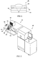
- FIG. 1 is a schematic sectional view of a wafer level image module in accordance with a first preferred embodiment of the present invention;
- FIG 2 is a perspective view of a wafer level image module assembly apparatus according to the present invention;
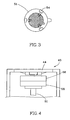
- FIG. 3 is a schematic view showing the clamping device clamped the stacked first water and the second wafer on the test table;
- FIG. 4 is a schematic side view showing the first water and the second wafer stacked together and placed on the test table;
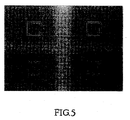
- FIG. 5 is a schematic drawing showing an out-of-focus status of an image mapped on the photo sensor according to the present invention;
- FIG. 6 is similar to FIG 4, showing the adjustment member set in between the first wafer (photo sensors) and the second wafer (lens sets);
- FIG 7 is a schematic drawing showing an image mapped onto the photo sensor after installation of the adjustment member in the wafer level image module according to the present invention;
- FIG. 8 is schematic drawing showing an in-focus status of an image mapped on the photo sensor according to the present invention;
- FIG. 9 is a schematic sectional view of a wafer level image module in accordance with a second preferred embodiment of the present invention;
- FIG 10 is a schematic sectional view of a wafer level image module in accordance with a third preferred embodiment of the present invention;
- FIG. 11 is a schematic sectional view of a wafer level image module in accordance with a fourth preferred embodiment of the present invention;
- FIG. 12 is a schematic drawing showing an image module according to the prior art, and
- FIG. 13 is a schematic drawing showing another design of image module according to the prior art.
- As shown in FIG. 1, a wafer
level image module 10 in accordance with a first preferred embodiment of the present invention comprises aphoto sensor 20, anadjustment member 25, and a lens set 30. Thephoto sensor 20 can be a CMOS (Complementary Metal-Oxide Semiconductor) image sensor or CCD (Charge Coupled Device) image sensor adapted to output an electrical signal when induced by light. Thephoto sensor 20 is mounted on the top side thereof with a lighttransmissive spacer 22. The lighttransmissive spacer 22 protects thephoto sensor 20 against outside pollutants and moisture. Theadjustment member 25 can be aglass ball spacer 25 or fiber spacer formed on the top surface of thetransmissive spacer 22 by sputtering deposition, spot adhesive, or screen printing. Theadjustment member 25 has a thickness about 1-50 µ m. This thickness is determined subject to the depth of focus required and the focus offset. Further, theadjustment member 25 can be formed on the transmissive spacer by means of thick film photolithography technology, or directly made of a glass plate. Alternatively, theadjustment member 25 can be formed on the lens set 30. - The
lens set 30 can be molded from transparent ultraviolet polymers, or made by etching. Thelens set 30 is covered on the top side of theadjustment member 25 such that theadjustment member 25 is sandwiched between the lens set 30 and thephoto sensor 20 for controlling the distance between the lens set 30 and thephoto sensor 20. Incident light rays go through the lens set 30 to thephoto sensor 20, thereby mapping the image onto thephoto sensor 30. The focus offset in which the lens set 30 maps the image of incident light rays onto thephoto sensor 20 is about 0-50 µm. When setting theadjustment member 25 in between the lens set 30 and thephoto sensor 20, the thickness of theadjustment member 25 compensates the focus offset, thereby controlling the precision of the focal distance of the lens set 30 within the desired depth of focus. For an image module of FNO equal to 2.8 and pixel size 3.6 µm, the focus precision is about 10 µm. By means of theadjustment member 25 to compensate light rays, incident light rays are accurately focused on thephoto sensor 20. - When making the aforesaid wafer
level image module 10, anassembly apparatus 40 is used for in-situ assembly and in-situ test of waferlevel image modules 10. The structure of thisassembly apparatus 40 is outlined hereinafter with reference to FIGS. 2 through 4. - As illustrated in FIGS. 2-4, the
assembly apparatus 40 comprises apositioning unit 42, asignal pickup device 43, asignal processor 46, and abonding unit 48. Thepositioning unit 42 comprises abase 50 and a test table 51. Thebase 50 supports a slidingcarrier 52 and aclamping device 54. The slidingcarrier 52 is movable in and out of the base 50 to carry waferlevel image modules 10. The clampingdevice 54 is adapted to hold waferlevel image modules 10 in position and to place waferlevel image modules 10 on the test table 51. Thesignal pickup device 43 comprises aprobe card 44. Thesignal pickup device 43 is mounted in thebase 50 of thepositioning unit 42. Thesignal processor 46 is electrically connected to thesignal pickup device 43, and adapted to check in-focus or out-of-focus status of the image signal picked up from waferlevel image modules 10. Thebonding unit 48 is adapted to bond thephoto sensor 20,adjustment member 25 and lens set 30 of waferlevel image modules 10. - The assembly process of the wafer
level image module 10 by theassembly apparatus 40 includes the following steps. - Step I: Perform an integrated circuit manufacturing process to-prepare a
first wafer 56. As shown in FIG 2, the first wafer has a plurality ofphoto sensors 20 each carrying a first alignment mark (not shown). - Step II: Perform an integrated circuit manufacturing process to prepare a
second wafer 58, which has a plurality of lens sets 30 each carrying a second alignment mark (not shown). - Step III: Place the
first water 56 in the slidingcarrier 52 of theassembly apparatus 40 and then stack thesecond wafer 58 on thefirst wafer 56 to have the second alignment marks of the lens sets 30 in alignment with the first alignment marks of thephoto sensors 20 respectively, and then, as shown in FIG 3, use theclamping device 54 to pre-bond thefirst wafer 56 and thesecond wafer 58 and to place the stackedfirst water 56 andsecond wafer 58 on the test table 51 to have thephoto sensors 20 correspond to theprobe card 44. - Step IV: Control the test table 51 to electrically connect the stacked
first water 56 andsecond wafer 58 to theprobe card 44, as shown in FIG. 4. The test table 50 can move the stackedwafers first water 56 and thesecond wafer 58 subject to test requirements. - Step V: Operate the
signal processor 46 to receive electrical signal from thesignal pickup device 43 so as to obtain the focus offset in which the respective lens sets 30 map the image of incident light rays onto therespective photo sensors 20 for determining in-focus or out-of-focus status of the photo sensors 20 (see FIG. 5) and discriminating far coal or near focal status in case of out-of-focus status. - Step VI: Move the sliding
carrier 52 out of thebase 50, and then apply theprepared adjustment member 25 to thefirst wafer 56 and thesecond wafer 58 to have theadjustment member 25 be sandwiched between the lens sets 30 and thephoto sensors 20, as shown in FIG. 6, and then electrically connect the integrated wafer level image modules of the stack ofwafers adjustment member 25 to theprobe card 44. - Step VII: Repeat the aforesaid steps IV through VI if the improved image, as shown in FIG 7, produced by the
photo sensors 20 still lightly shows an out-of-focus status till the in-focus status shown in FIG. 8 where theadjustment member 25 accurately compensates the focus offset. - Step VIII: Operate the
clamping device 54 to hold tight thefirst wafer 56 and thesecond wafer 58, and then operate thebonding unit 48 to bond thefirst wafer 56, theadjustment member 25 and thesecond wafer 58 together. - Step IX: Cut the stacked
wafers adjustment member 25 into single chips, i.e., individual waferlevel image modules 10. - When the lens sets 30 of the
second wafer 58 are stacked on thephoto sensors 20 of thefirst wafer 56 by means of theaforesaid assembly apparatus 40 and the aforesaid assembly process, thesignal processor 46 is used to check in-focus or out-of-focus status of the electrical signal received from the signal pickup device through thephoto sensors 20. If thephoto sensors 20 are at an out-of-focus status, the thickness of theadjustment member 25 is adjusted to correct the out-of-focus status of thephoto sensors 20 to an in-focus status, assuring image quality of the assembled waferlevel image modules 10. Further, by means of changing the thickness of theadjustment member 25, the distance between the respective lens sets 30 and therespective photo sensors 20 is relatively adjusted, thereby accurately compensating the focus offset between the respective lens sets 30 and therespective photo sensors 20 so that the respective lens sets 30 accurately focus light rays onto therespective photo sensors 20. - As stated above, the invention uses the structure of the adjustment member to have the wafer level image module provide a better image quality.
- FIG 9 shows a wafer
level image module 60 in accordance with a second embodiment of the present invention. Similar to the aforesaid first embodiment of the present invention, the waferlevel image module 60 comprises aphoto sensor 61, a lens set 62, and anadjustment member 63 sandwiched between thephoto sensor 60 and the lens set 62. The main feature of this second embodiment is that the lens set 62 comprises afirst lens layer 64, asecond lens layer 65, afirst transmissive pad 66 sandwiched between thefirst lens layer 64 and thesecond lens layer 65, and asecond transmissive pad 67 bonded to the top surface of thesecond lens layer 65 opposite to thefirst transmissive pad 66. Thefirst lens layer 64 is bonded to theadjustment member 63 above thephoto sensor 61. Thefirst lens layer 64 and thesecond lens layer 65 are transparent for mapping the image of incident light rays onto thephoto sensor 61. This lens set 62 enables the waferlevel image module 60 to have more image characteristics. - FIG. 10 shows a wafer
level image module 70 in accordance with a third embodiment of the present invention. This third embodiment is substantially similar to the aforesaid second embodiment with the exception that thetransmissive spacer 72 on thephoto sensor 71 has anopening 73 corresponding to the photo sensing area of thephoto sensor 71. This third embodiment achieves the same various effects as the aforesaid first and second embodiments of the present invention. - FIG 11 shows a wafer
level image module 75 in accordance with a fourth embodiment of the present invention. According to this fourth embodiment, theadjustment member 76 is directly bonded to the surface of thephoto sensor 77, and thefirst lens layer 79 of the lens set 78 is bonded to theadjustment member 76. This fourth embodiment achieves the same various effects as the aforesaid various embodiments of the present invention. - The invention being thus described, it will be obvious that the same may be varied in many ways. Such variations are not to be regarded as a departure from the spirit and scope of the invention, and all such modifications as would be obvious to one skilled in the art are intended to be included within the scope of the following claims.
Claims (15)
- A wafer level image module comprising:a photo sensor for outputting an electrical signal upon receiving light;a lens set for focusing incident light onto the photo sensor; andan adjustment member disposed between the photo sensor and the lens set for controlling the distance between the photo sensor and the lens set for enabling the lens set to focus the incident light onto the photo sensor in an in-focus manner.
- The wafer level image module as claimed in claim 1, wherein the lens set comprises a first transparent lens layer bonded to the adjustment member, a second transparent lens layer, and a light transmissive pad sandwiched between the first transparent lens layer and the second transparent lens layer.
- The wafer level image module as claimed in claim 1, wherein the lens set further comprises a light transmissive pad bonded to a top surface of the second transparent lens layer opposite to the light transmissive pad that is sandwiched between the first transparent lens layer and the second transparent lens layer.
- The wafer level image module as claimed in claim 1, further comprising a transparent spacer disposed between the photo sensor and the adjustment member.
- The wafer level image module as claimed in claim 4, wherein the transparent spacer has an opening corresponding to a photo sensing area of the photo sensor.
- The wafer level image module as claimed in claim 1, wherein the adjustment member comprises a glass ball spacer or a fiber spacer.
- The wafer level image module as claimed in claim 1, wherein said photo sensor is a complementary metal-oxide semiconductor type photo sensor.
- The wafer level image module as claimed in claim 1, wherein said adjustment member has a thickness substantially ranging 1-50 µm.
- The wafer level image module as claimed in claim 1, wherein said adjustment member is made by means of thick film photolithography technology.
- A method for making a wafer level image module comprising the steps of:a) providing a photo sensor made by an integrated circuit manufacturing process;b) stacking a lens set made by an integrated circuit manufacturing process on the photo sensor;c) measuring a focus offset of said lens set and determining in-focus or out-of-focus status of said photo sensor; andd) disposing an adjustment member between said lens set and said photo sensor to compensate the focus offset of said lens set so as to have said photo sensor be in an in-focus status.
- The method as claimed in claim 10, wherein said step (c) comprises a sub-step of using a signal processor to check the out-of-focus status to be a far focal or near focal status when said photo sensor is in an out-of-focus status.
- An apparatus for in-situ assembling and testing the wafer level image module of claim 1, the apparatus comprising:a positioning unit for positioning said photo sensor on said lens set and for setting said adjustment member between said photo sensor on said lens set;a signal pickup device electrically connected to said photo sensor for picking up a signal from said photo sensor upon focusing of an image onto said photo sensor by said lens set;a signal processor electrically connected to said signal pickup device for determining in-focus or out-of-focus status of the image focusing on the photo sensor; anda bonding unit for bonding said photo sensor, said adjustment member and said lens set together.
- The apparatus as claimed in claim 12, wherein said positioning unit comprises a clamping device for clamping said photo sensor, said adjustment member and said lens set together for bonding by said bonding unit.
- The apparatus as claimed in claim 12, wherein said positioning unit comprises a test table for carrying said wafer level image module and electrically connecting said wafer level image module to said signal pickup device.
- The apparatus as claimed in claim 12, wherein said signal pickup device comprises a probe card electrically connected to said photo sensor of said wafer level image module.
Applications Claiming Priority (1)
| Application Number | Priority Date | Filing Date | Title |
|---|---|---|---|
| CN2005101134502A CN1945857B (en) | 2005-10-09 | 2005-10-09 | Wafer Level Image Module |
Publications (3)
| Publication Number | Publication Date |
|---|---|
| EP1772908A2 true EP1772908A2 (en) | 2007-04-11 |
| EP1772908A3 EP1772908A3 (en) | 2008-10-22 |
| EP1772908B1 EP1772908B1 (en) | 2018-10-03 |
Family
ID=37672240
Family Applications (1)
| Application Number | Title | Priority Date | Filing Date |
|---|---|---|---|
| EP06020946.7A Active EP1772908B1 (en) | 2005-10-09 | 2006-10-05 | Wafer level image module, method for making the same and apparatus for assembling and testing the same |
Country Status (2)
| Country | Link |
|---|---|
| EP (1) | EP1772908B1 (en) |
| CN (1) | CN1945857B (en) |
Cited By (3)
| Publication number | Priority date | Publication date | Assignee | Title |
|---|---|---|---|---|
| WO2009141327A1 (en) * | 2008-05-21 | 2009-11-26 | Commissariat A L'energie Atomique | Method of producing an optical device consisting of integrated optoelectronic components |
| US7710667B2 (en) | 2008-06-25 | 2010-05-04 | Aptina Imaging Corp. | Imaging module with symmetrical lens system and method of manufacture |
| US7773317B2 (en) | 2008-07-01 | 2010-08-10 | Aptina Imaging Corp. | Lens system with symmetrical optics |
Families Citing this family (1)
| Publication number | Priority date | Publication date | Assignee | Title |
|---|---|---|---|---|
| CN103581572A (en) * | 2012-08-01 | 2014-02-12 | 奇景光电股份有限公司 | Wafer-level optical module and combination method thereof |
Family Cites Families (10)
| Publication number | Priority date | Publication date | Assignee | Title |
|---|---|---|---|---|
| JP2000134528A (en) * | 1998-10-21 | 2000-05-12 | Konica Corp | Method for positioning solid-state image pickup element and method for adjusting digital still camera and holding member |
| US6370225B1 (en) * | 2000-12-27 | 2002-04-09 | Caresbuilt Inc. | Image receptor for an x-ray apparatus |
| US6603614B2 (en) * | 2001-01-26 | 2003-08-05 | Corning Precision Lens, Inc. | Lens assembly having automatic thermal focus adjustment |
| US6635941B2 (en) * | 2001-03-21 | 2003-10-21 | Canon Kabushiki Kaisha | Structure of semiconductor device with improved reliability |
| CN1151397C (en) * | 2001-07-17 | 2004-05-26 | 哈尔滨工业大学 | Adjusting the Inner Focusing Telescope of Infrared Laser Grating Resonator |
| JP5004412B2 (en) * | 2003-07-24 | 2012-08-22 | パナソニック株式会社 | Manufacturing method and manufacturing apparatus for lens-integrated imaging device |
| US20050067681A1 (en) * | 2003-09-26 | 2005-03-31 | Tessera, Inc. | Package having integral lens and wafer-scale fabrication method therefor |
| DE10344770A1 (en) * | 2003-09-26 | 2005-05-04 | Siemens Ag | Optical module and optical system |
| US7583862B2 (en) * | 2003-11-26 | 2009-09-01 | Aptina Imaging Corporation | Packaged microelectronic imagers and methods of packaging microelectronic imagers |
| JP4476764B2 (en) * | 2004-03-26 | 2010-06-09 | 富士フイルム株式会社 | Substrate bonding apparatus and method |
-
2005
- 2005-10-09 CN CN2005101134502A patent/CN1945857B/en not_active Expired - Lifetime
-
2006
- 2006-10-05 EP EP06020946.7A patent/EP1772908B1/en active Active
Cited By (5)
| Publication number | Priority date | Publication date | Assignee | Title |
|---|---|---|---|---|
| WO2009141327A1 (en) * | 2008-05-21 | 2009-11-26 | Commissariat A L'energie Atomique | Method of producing an optical device consisting of integrated optoelectronic components |
| FR2931587A1 (en) * | 2008-05-21 | 2009-11-27 | Commissariat Energie Atomique | METHOD FOR PRODUCING AN OPTICAL DEVICE WITH INTEGRATED OPTOELECTRONIC COMPONENTS |
| US8124439B2 (en) | 2008-05-21 | 2012-02-28 | Commissariat A L'energie Atomique Et Aux Energies Alternatives | Method for making an optical device with integrated optoelectronic components |
| US7710667B2 (en) | 2008-06-25 | 2010-05-04 | Aptina Imaging Corp. | Imaging module with symmetrical lens system and method of manufacture |
| US7773317B2 (en) | 2008-07-01 | 2010-08-10 | Aptina Imaging Corp. | Lens system with symmetrical optics |
Also Published As
| Publication number | Publication date |
|---|---|
| EP1772908B1 (en) | 2018-10-03 |
| CN1945857B (en) | 2012-06-27 |
| CN1945857A (en) | 2007-04-11 |
| EP1772908A3 (en) | 2008-10-22 |
Similar Documents
| Publication | Publication Date | Title |
|---|---|---|
| US8524521B2 (en) | Method for making wafer level image module | |
| KR101032391B1 (en) | Electronic device wafer module, electronic device module, sensor wafer module, sensor module, lens array plate, sensor module manufacturing method and electronic information device | |
| CN101281286B (en) | Solid-state imaging device and electronic equipment having the same | |
| JP4793618B2 (en) | CMOS image sensor structure and process for manufacturing a camera module using the same | |
| TWI336590B (en) | Semiconductor package, semiconductor module and production method thereof, and electronic device | |
| CN101459165B (en) | Electronic component wafer module, manufacturing method thereof and electronic information device | |
| US20110096213A1 (en) | Wafer-shaped optical apparatus and manufacturing method thereof, electronic element wafer module, sensor wafer module, electronic element module,sensor module, and electronic information device | |
| US20090015706A1 (en) | Auto focus/zoom modules using wafer level optics | |
| US20110026148A1 (en) | Actuator array sheet | |
| US20060186317A1 (en) | Methods for packaging microelectronic imagers | |
| JP2004226872A (en) | Camera module and manufacturing method thereof | |
| WO2004010679A2 (en) | Camera module, camera system and method of manufacturing a camera module | |
| US7728398B2 (en) | Micro camera module and method of manufacturing the same | |
| CN101494721A (en) | Image capturing module, method for manufacturing the image capturing module, and electronic information device | |
| EP1772908B1 (en) | Wafer level image module, method for making the same and apparatus for assembling and testing the same | |
| JP2004233482A (en) | Method of manufacturing camera module | |
| US20080246873A1 (en) | Solid-state image sensing device and electronic apparatus comprising same | |
| JP2004260357A (en) | The camera module | |
| CN106961539B (en) | Array camera module and manufacturing method thereof | |
| JP2004260356A (en) | The camera module | |
| KR100945443B1 (en) | Wafer level camera module | |
| CN119447001A (en) | A bonding alignment system, bonding equipment and bonding method | |
| JP2004246220A (en) | Camera module and manufacturing method thereof | |
| JP2009071187A (en) | Manufacturing method of solid-state imaging device | |
| JP2004242205A (en) | Camera module and manufacturing method thereof |
Legal Events
| Date | Code | Title | Description |
|---|---|---|---|
| PUAI | Public reference made under article 153(3) epc to a published international application that has entered the european phase |
Free format text: ORIGINAL CODE: 0009012 |
|
| 17P | Request for examination filed |
Effective date: 20061005 |
|
| AK | Designated contracting states |
Kind code of ref document: A2 Designated state(s): AT BE BG CH CY CZ DE DK EE ES FI FR GB GR HU IE IS IT LI LT LU LV MC NL PL PT RO SE SI SK TR |
|
| AX | Request for extension of the european patent |
Extension state: AL BA HR MK YU |
|
| PUAL | Search report despatched |
Free format text: ORIGINAL CODE: 0009013 |
|
| AK | Designated contracting states |
Kind code of ref document: A3 Designated state(s): AT BE BG CH CY CZ DE DK EE ES FI FR GB GR HU IE IS IT LI LT LU LV MC NL PL PT RO SE SI SK TR |
|
| AX | Request for extension of the european patent |
Extension state: AL BA HR MK RS |
|
| 17Q | First examination report despatched |
Effective date: 20090108 |
|
| AKX | Designation fees paid |
Designated state(s): AT BE BG CH CY CZ DE DK EE ES FI FR GB GR HU IE IS IT LI LT LU LV MC NL PL PT RO SE SI SK TR |
|
| RAP1 | Party data changed (applicant data changed or rights of an application transferred) |
Owner name: OMNIVISION TECHNOLOGIES, INC. Owner name: VISERA TECHNOLOGIES COMPANY LTD. |
|
| RIC1 | Information provided on ipc code assigned before grant |
Ipc: H01L 27/146 20060101ALI20180404BHEP Ipc: H01L 31/0232 20060101AFI20180404BHEP Ipc: H04N 17/00 20060101ALI20180404BHEP Ipc: H04N 5/225 20060101ALI20180404BHEP |
|
| GRAP | Despatch of communication of intention to grant a patent |
Free format text: ORIGINAL CODE: EPIDOSNIGR1 |
|
| STAA | Information on the status of an ep patent application or granted ep patent |
Free format text: STATUS: GRANT OF PATENT IS INTENDED |
|
| RAP1 | Party data changed (applicant data changed or rights of an application transferred) |
Owner name: VISERA TECHNOLOGIES, COMPANY LTD. Owner name: OMNIVISION TECHNOLOGIES, INC. |
|
| INTG | Intention to grant announced |
Effective date: 20180528 |
|
| RAP1 | Party data changed (applicant data changed or rights of an application transferred) |
Owner name: OMNIVISION TECHNOLOGIES, INC. Owner name: VISERA TECHNOLOGIES COMPANY LIMITED |
|
| GRAS | Grant fee paid |
Free format text: ORIGINAL CODE: EPIDOSNIGR3 |
|
| GRAA | (expected) grant |
Free format text: ORIGINAL CODE: 0009210 |
|
| STAA | Information on the status of an ep patent application or granted ep patent |
Free format text: STATUS: THE PATENT HAS BEEN GRANTED |
|
| REG | Reference to a national code |
Ref country code: FR Ref legal event code: PLFP Year of fee payment: 13 |
|
| AK | Designated contracting states |
Kind code of ref document: B1 Designated state(s): AT BE BG CH CY CZ DE DK EE ES FI FR GB GR HU IE IS IT LI LT LU LV MC NL PL PT RO SE SI SK TR |
|
| REG | Reference to a national code |
Ref country code: GB Ref legal event code: FG4D |
|
| REG | Reference to a national code |
Ref country code: CH Ref legal event code: EP Ref country code: AT Ref legal event code: REF Ref document number: 1049557 Country of ref document: AT Kind code of ref document: T Effective date: 20181015 |
|
| REG | Reference to a national code |
Ref country code: DE Ref legal event code: R096 Ref document number: 602006056471 Country of ref document: DE |
|
| REG | Reference to a national code |
Ref country code: IE Ref legal event code: FG4D Ref country code: NL Ref legal event code: FP |
|
| REG | Reference to a national code |
Ref country code: LT Ref legal event code: MG4D |
|
| REG | Reference to a national code |
Ref country code: AT Ref legal event code: MK05 Ref document number: 1049557 Country of ref document: AT Kind code of ref document: T Effective date: 20181003 |
|
| PG25 | Lapsed in a contracting state [announced via postgrant information from national office to epo] |
Ref country code: ES Free format text: LAPSE BECAUSE OF FAILURE TO SUBMIT A TRANSLATION OF THE DESCRIPTION OR TO PAY THE FEE WITHIN THE PRESCRIBED TIME-LIMIT Effective date: 20181003 Ref country code: CZ Free format text: LAPSE BECAUSE OF FAILURE TO SUBMIT A TRANSLATION OF THE DESCRIPTION OR TO PAY THE FEE WITHIN THE PRESCRIBED TIME-LIMIT Effective date: 20181003 Ref country code: LV Free format text: LAPSE BECAUSE OF FAILURE TO SUBMIT A TRANSLATION OF THE DESCRIPTION OR TO PAY THE FEE WITHIN THE PRESCRIBED TIME-LIMIT Effective date: 20181003 Ref country code: PL Free format text: LAPSE BECAUSE OF FAILURE TO SUBMIT A TRANSLATION OF THE DESCRIPTION OR TO PAY THE FEE WITHIN THE PRESCRIBED TIME-LIMIT Effective date: 20181003 Ref country code: BG Free format text: LAPSE BECAUSE OF FAILURE TO SUBMIT A TRANSLATION OF THE DESCRIPTION OR TO PAY THE FEE WITHIN THE PRESCRIBED TIME-LIMIT Effective date: 20190103 Ref country code: FI Free format text: LAPSE BECAUSE OF FAILURE TO SUBMIT A TRANSLATION OF THE DESCRIPTION OR TO PAY THE FEE WITHIN THE PRESCRIBED TIME-LIMIT Effective date: 20181003 Ref country code: LT Free format text: LAPSE BECAUSE OF FAILURE TO SUBMIT A TRANSLATION OF THE DESCRIPTION OR TO PAY THE FEE WITHIN THE PRESCRIBED TIME-LIMIT Effective date: 20181003 Ref country code: IS Free format text: LAPSE BECAUSE OF FAILURE TO SUBMIT A TRANSLATION OF THE DESCRIPTION OR TO PAY THE FEE WITHIN THE PRESCRIBED TIME-LIMIT Effective date: 20190203 Ref country code: AT Free format text: LAPSE BECAUSE OF FAILURE TO SUBMIT A TRANSLATION OF THE DESCRIPTION OR TO PAY THE FEE WITHIN THE PRESCRIBED TIME-LIMIT Effective date: 20181003 |
|
| PG25 | Lapsed in a contracting state [announced via postgrant information from national office to epo] |
Ref country code: SE Free format text: LAPSE BECAUSE OF FAILURE TO SUBMIT A TRANSLATION OF THE DESCRIPTION OR TO PAY THE FEE WITHIN THE PRESCRIBED TIME-LIMIT Effective date: 20181003 Ref country code: GR Free format text: LAPSE BECAUSE OF FAILURE TO SUBMIT A TRANSLATION OF THE DESCRIPTION OR TO PAY THE FEE WITHIN THE PRESCRIBED TIME-LIMIT Effective date: 20190104 Ref country code: PT Free format text: LAPSE BECAUSE OF FAILURE TO SUBMIT A TRANSLATION OF THE DESCRIPTION OR TO PAY THE FEE WITHIN THE PRESCRIBED TIME-LIMIT Effective date: 20190203 |
|
| REG | Reference to a national code |
Ref country code: BE Ref legal event code: MM Effective date: 20181031 |
|
| PG25 | Lapsed in a contracting state [announced via postgrant information from national office to epo] |
Ref country code: LU Free format text: LAPSE BECAUSE OF NON-PAYMENT OF DUE FEES Effective date: 20181005 |
|
| REG | Reference to a national code |
Ref country code: DE Ref legal event code: R097 Ref document number: 602006056471 Country of ref document: DE |
|
| REG | Reference to a national code |
Ref country code: IE Ref legal event code: MM4A |
|
| PG25 | Lapsed in a contracting state [announced via postgrant information from national office to epo] |
Ref country code: DK Free format text: LAPSE BECAUSE OF FAILURE TO SUBMIT A TRANSLATION OF THE DESCRIPTION OR TO PAY THE FEE WITHIN THE PRESCRIBED TIME-LIMIT Effective date: 20181003 Ref country code: IT Free format text: LAPSE BECAUSE OF FAILURE TO SUBMIT A TRANSLATION OF THE DESCRIPTION OR TO PAY THE FEE WITHIN THE PRESCRIBED TIME-LIMIT Effective date: 20181003 |
|
| PLBE | No opposition filed within time limit |
Free format text: ORIGINAL CODE: 0009261 |
|
| STAA | Information on the status of an ep patent application or granted ep patent |
Free format text: STATUS: NO OPPOSITION FILED WITHIN TIME LIMIT |
|
| PG25 | Lapsed in a contracting state [announced via postgrant information from national office to epo] |
Ref country code: SK Free format text: LAPSE BECAUSE OF FAILURE TO SUBMIT A TRANSLATION OF THE DESCRIPTION OR TO PAY THE FEE WITHIN THE PRESCRIBED TIME-LIMIT Effective date: 20181003 Ref country code: RO Free format text: LAPSE BECAUSE OF FAILURE TO SUBMIT A TRANSLATION OF THE DESCRIPTION OR TO PAY THE FEE WITHIN THE PRESCRIBED TIME-LIMIT Effective date: 20181003 Ref country code: BE Free format text: LAPSE BECAUSE OF NON-PAYMENT OF DUE FEES Effective date: 20181031 Ref country code: MC Free format text: LAPSE BECAUSE OF FAILURE TO SUBMIT A TRANSLATION OF THE DESCRIPTION OR TO PAY THE FEE WITHIN THE PRESCRIBED TIME-LIMIT Effective date: 20181003 Ref country code: EE Free format text: LAPSE BECAUSE OF FAILURE TO SUBMIT A TRANSLATION OF THE DESCRIPTION OR TO PAY THE FEE WITHIN THE PRESCRIBED TIME-LIMIT Effective date: 20181003 |
|
| 26N | No opposition filed |
Effective date: 20190704 |
|
| PG25 | Lapsed in a contracting state [announced via postgrant information from national office to epo] |
Ref country code: SI Free format text: LAPSE BECAUSE OF FAILURE TO SUBMIT A TRANSLATION OF THE DESCRIPTION OR TO PAY THE FEE WITHIN THE PRESCRIBED TIME-LIMIT Effective date: 20181003 Ref country code: IE Free format text: LAPSE BECAUSE OF NON-PAYMENT OF DUE FEES Effective date: 20181005 |
|
| PG25 | Lapsed in a contracting state [announced via postgrant information from national office to epo] |
Ref country code: TR Free format text: LAPSE BECAUSE OF FAILURE TO SUBMIT A TRANSLATION OF THE DESCRIPTION OR TO PAY THE FEE WITHIN THE PRESCRIBED TIME-LIMIT Effective date: 20181003 |
|
| PG25 | Lapsed in a contracting state [announced via postgrant information from national office to epo] |
Ref country code: HU Free format text: LAPSE BECAUSE OF FAILURE TO SUBMIT A TRANSLATION OF THE DESCRIPTION OR TO PAY THE FEE WITHIN THE PRESCRIBED TIME-LIMIT; INVALID AB INITIO Effective date: 20061005 Ref country code: CY Free format text: LAPSE BECAUSE OF FAILURE TO SUBMIT A TRANSLATION OF THE DESCRIPTION OR TO PAY THE FEE WITHIN THE PRESCRIBED TIME-LIMIT Effective date: 20181003 |
|
| P01 | Opt-out of the competence of the unified patent court (upc) registered |
Effective date: 20230620 |
|
| REG | Reference to a national code |
Ref country code: DE Ref legal event code: R079 Ref document number: 602006056471 Country of ref document: DE Free format text: PREVIOUS MAIN CLASS: H01L0031023200 Ipc: H10F0077400000 |
|
| REG | Reference to a national code |
Ref country code: CH Ref legal event code: U11 Free format text: ST27 STATUS EVENT CODE: U-0-0-U10-U11 (AS PROVIDED BY THE NATIONAL OFFICE) Effective date: 20251101 |
|
| PGFP | Annual fee paid to national office [announced via postgrant information from national office to epo] |
Ref country code: NL Payment date: 20251026 Year of fee payment: 20 |
|
| PGFP | Annual fee paid to national office [announced via postgrant information from national office to epo] |
Ref country code: DE Payment date: 20251029 Year of fee payment: 20 |
|
| PGFP | Annual fee paid to national office [announced via postgrant information from national office to epo] |
Ref country code: GB Payment date: 20251027 Year of fee payment: 20 |
|
| PGFP | Annual fee paid to national office [announced via postgrant information from national office to epo] |
Ref country code: FR Payment date: 20251027 Year of fee payment: 20 |
|
| PGFP | Annual fee paid to national office [announced via postgrant information from national office to epo] |
Ref country code: CH Payment date: 20251101 Year of fee payment: 20 |
|
| REG | Reference to a national code |
Ref country code: CH Ref legal event code: R17 Free format text: ST27 STATUS EVENT CODE: U-0-0-R10-R17 (AS PROVIDED BY THE NATIONAL OFFICE) Effective date: 20260410 |