EP1770709A1 - Memory device comprising an array of resistive memory cells with bit lines precharging - Google Patents
Memory device comprising an array of resistive memory cells with bit lines precharging Download PDFInfo
- Publication number
- EP1770709A1 EP1770709A1 EP05021351A EP05021351A EP1770709A1 EP 1770709 A1 EP1770709 A1 EP 1770709A1 EP 05021351 A EP05021351 A EP 05021351A EP 05021351 A EP05021351 A EP 05021351A EP 1770709 A1 EP1770709 A1 EP 1770709A1
- Authority
- EP
- European Patent Office
- Prior art keywords
- bit line
- resistive memory
- charging
- resistive
- bit lines
- Prior art date
- Legal status (The legal status is an assumption and is not a legal conclusion. Google has not performed a legal analysis and makes no representation as to the accuracy of the status listed.)
- Granted
Links
- 230000015654 memory Effects 0.000 title claims abstract description 109
- 238000011156 evaluation Methods 0.000 claims abstract description 34
- 239000007784 solid electrolyte Substances 0.000 claims description 11
- 239000005083 Zinc sulfide Substances 0.000 claims description 6
- 229910052980 cadmium sulfide Inorganic materials 0.000 claims description 6
- 229940116367 cadmium sulfide Drugs 0.000 claims description 6
- 239000010949 copper Substances 0.000 claims description 6
- 239000011734 sodium Substances 0.000 claims description 6
- 229910052984 zinc sulfide Inorganic materials 0.000 claims description 6
- 229940063789 zinc sulfide Drugs 0.000 claims description 6
- PFNQVRZLDWYSCW-UHFFFAOYSA-N (fluoren-9-ylideneamino) n-naphthalen-1-ylcarbamate Chemical compound C12=CC=CC=C2C2=CC=CC=C2C1=NOC(=O)NC1=CC=CC2=CC=CC=C12 PFNQVRZLDWYSCW-UHFFFAOYSA-N 0.000 claims description 5
- WUPHOULIZUERAE-UHFFFAOYSA-N 3-(oxolan-2-yl)propanoic acid Chemical compound OC(=O)CCC1CCCO1 WUPHOULIZUERAE-UHFFFAOYSA-N 0.000 claims description 5
- KHDSWONFYIAAPE-UHFFFAOYSA-N silicon sulfide Chemical compound S=[Si]=S KHDSWONFYIAAPE-UHFFFAOYSA-N 0.000 claims description 5
- OCGWQDWYSQAFTO-UHFFFAOYSA-N tellanylidenelead Chemical compound [Pb]=[Te] OCGWQDWYSQAFTO-UHFFFAOYSA-N 0.000 claims description 5
- 229910005842 GeS2 Inorganic materials 0.000 claims description 3
- 229910005866 GeSe Inorganic materials 0.000 claims description 3
- 229910005867 GeSe2 Inorganic materials 0.000 claims description 3
- 229910002665 PbTe Inorganic materials 0.000 claims description 3
- 229910052802 copper Inorganic materials 0.000 claims description 3
- 229910052744 lithium Inorganic materials 0.000 claims description 3
- 229910052709 silver Inorganic materials 0.000 claims description 3
- 239000004332 silver Substances 0.000 claims description 3
- 229910052708 sodium Inorganic materials 0.000 claims description 3
- 230000000694 effects Effects 0.000 description 9
- 239000000463 material Substances 0.000 description 5
- 230000008878 coupling Effects 0.000 description 4
- 238000010168 coupling process Methods 0.000 description 4
- 238000005859 coupling reaction Methods 0.000 description 4
- 238000007667 floating Methods 0.000 description 4
- 230000010354 integration Effects 0.000 description 4
- 230000003071 parasitic effect Effects 0.000 description 4
- JBQYATWDVHIOAR-UHFFFAOYSA-N tellanylidenegermanium Chemical compound [Te]=[Ge] JBQYATWDVHIOAR-UHFFFAOYSA-N 0.000 description 4
- 230000008901 benefit Effects 0.000 description 3
- 239000003990 capacitor Substances 0.000 description 3
- 238000004519 manufacturing process Methods 0.000 description 3
- 229910021645 metal ion Inorganic materials 0.000 description 3
- QIHHYQWNYKOHEV-UHFFFAOYSA-N 4-tert-butyl-3-nitrobenzoic acid Chemical compound CC(C)(C)C1=CC=C(C(O)=O)C=C1[N+]([O-])=O QIHHYQWNYKOHEV-UHFFFAOYSA-N 0.000 description 2
- RYGMFSIKBFXOCR-UHFFFAOYSA-N Copper Chemical compound [Cu] RYGMFSIKBFXOCR-UHFFFAOYSA-N 0.000 description 2
- DGAQECJNVWCQMB-PUAWFVPOSA-M Ilexoside XXIX Chemical compound C[C@@H]1CC[C@@]2(CC[C@@]3(C(=CC[C@H]4[C@]3(CC[C@@H]5[C@@]4(CC[C@@H](C5(C)C)OS(=O)(=O)[O-])C)C)[C@@H]2[C@]1(C)O)C)C(=O)O[C@H]6[C@@H]([C@H]([C@@H]([C@H](O6)CO)O)O)O.[Na+] DGAQECJNVWCQMB-PUAWFVPOSA-M 0.000 description 2
- WHXSMMKQMYFTQS-UHFFFAOYSA-N Lithium Chemical compound [Li] WHXSMMKQMYFTQS-UHFFFAOYSA-N 0.000 description 2
- BQCADISMDOOEFD-UHFFFAOYSA-N Silver Chemical compound [Ag] BQCADISMDOOEFD-UHFFFAOYSA-N 0.000 description 2
- AQCDIIAORKRFCD-UHFFFAOYSA-N cadmium selenide Chemical compound [Cd]=[Se] AQCDIIAORKRFCD-UHFFFAOYSA-N 0.000 description 2
- 230000008859 change Effects 0.000 description 2
- 238000013500 data storage Methods 0.000 description 2
- 230000001419 dependent effect Effects 0.000 description 2
- 230000005684 electric field Effects 0.000 description 2
- XCAUINMIESBTBL-UHFFFAOYSA-N lead(ii) sulfide Chemical compound [Pb]=S XCAUINMIESBTBL-UHFFFAOYSA-N 0.000 description 2
- 238000000034 method Methods 0.000 description 2
- GGYFMLJDMAMTAB-UHFFFAOYSA-N selanylidenelead Chemical compound [Pb]=[Se] GGYFMLJDMAMTAB-UHFFFAOYSA-N 0.000 description 2
- KSLZNZZNAHIBHL-UHFFFAOYSA-N selanylidenesilicon Chemical compound [Se]=[Si] KSLZNZZNAHIBHL-UHFFFAOYSA-N 0.000 description 2
- MFIWAIVSOUGHLI-UHFFFAOYSA-N selenium;tin Chemical compound [Sn]=[Se] MFIWAIVSOUGHLI-UHFFFAOYSA-N 0.000 description 2
- VDNSGQQAZRMTCI-UHFFFAOYSA-N sulfanylidenegermanium Chemical compound [Ge]=S VDNSGQQAZRMTCI-UHFFFAOYSA-N 0.000 description 2
- UURRKPRQEQXTBB-UHFFFAOYSA-N tellanylidenestannane Chemical compound [Te]=[SnH2] UURRKPRQEQXTBB-UHFFFAOYSA-N 0.000 description 2
- AFNRRBXCCXDRPS-UHFFFAOYSA-N tin(ii) sulfide Chemical compound [Sn]=S AFNRRBXCCXDRPS-UHFFFAOYSA-N 0.000 description 2
- DRDVZXDWVBGGMH-UHFFFAOYSA-N zinc;sulfide Chemical compound [S-2].[Zn+2] DRDVZXDWVBGGMH-UHFFFAOYSA-N 0.000 description 2
- 238000003491 array Methods 0.000 description 1
- 230000006735 deficit Effects 0.000 description 1
- 230000003111 delayed effect Effects 0.000 description 1
- 238000005516 engineering process Methods 0.000 description 1
- 230000006870 function Effects 0.000 description 1
- 230000002452 interceptive effect Effects 0.000 description 1
- 238000001459 lithography Methods 0.000 description 1
- 230000007257 malfunction Effects 0.000 description 1
- 238000001465 metallisation Methods 0.000 description 1
- 239000012782 phase change material Substances 0.000 description 1
- 230000000704 physical effect Effects 0.000 description 1
- 238000011176 pooling Methods 0.000 description 1
Images


Classifications
-
- G—PHYSICS
- G11—INFORMATION STORAGE
- G11C—STATIC STORES
- G11C13/00—Digital stores characterised by the use of storage elements not covered by groups G11C11/00, G11C23/00, or G11C25/00
- G11C13/0002—Digital stores characterised by the use of storage elements not covered by groups G11C11/00, G11C23/00, or G11C25/00 using resistive RAM [RRAM] elements
- G11C13/0007—Digital stores characterised by the use of storage elements not covered by groups G11C11/00, G11C23/00, or G11C25/00 using resistive RAM [RRAM] elements comprising metal oxide memory material, e.g. perovskites
-
- G—PHYSICS
- G11—INFORMATION STORAGE
- G11C—STATIC STORES
- G11C13/00—Digital stores characterised by the use of storage elements not covered by groups G11C11/00, G11C23/00, or G11C25/00
- G11C13/0002—Digital stores characterised by the use of storage elements not covered by groups G11C11/00, G11C23/00, or G11C25/00 using resistive RAM [RRAM] elements
- G11C13/0004—Digital stores characterised by the use of storage elements not covered by groups G11C11/00, G11C23/00, or G11C25/00 using resistive RAM [RRAM] elements comprising amorphous/crystalline phase transition cells
-
- G—PHYSICS
- G11—INFORMATION STORAGE
- G11C—STATIC STORES
- G11C13/00—Digital stores characterised by the use of storage elements not covered by groups G11C11/00, G11C23/00, or G11C25/00
- G11C13/0002—Digital stores characterised by the use of storage elements not covered by groups G11C11/00, G11C23/00, or G11C25/00 using resistive RAM [RRAM] elements
- G11C13/0009—RRAM elements whose operation depends upon chemical change
- G11C13/0011—RRAM elements whose operation depends upon chemical change comprising conductive bridging RAM [CBRAM] or programming metallization cells [PMCs]
-
- G—PHYSICS
- G11—INFORMATION STORAGE
- G11C—STATIC STORES
- G11C13/00—Digital stores characterised by the use of storage elements not covered by groups G11C11/00, G11C23/00, or G11C25/00
- G11C13/0002—Digital stores characterised by the use of storage elements not covered by groups G11C11/00, G11C23/00, or G11C25/00 using resistive RAM [RRAM] elements
- G11C13/0021—Auxiliary circuits
- G11C13/0023—Address circuits or decoders
- G11C13/0026—Bit-line or column circuits
-
- G—PHYSICS
- G11—INFORMATION STORAGE
- G11C—STATIC STORES
- G11C29/00—Checking stores for correct operation ; Subsequent repair; Testing stores during standby or offline operation
- G11C29/70—Masking faults in memories by using spares or by reconfiguring
- G11C29/78—Masking faults in memories by using spares or by reconfiguring using programmable devices
- G11C29/83—Masking faults in memories by using spares or by reconfiguring using programmable devices with reduced power consumption
- G11C29/832—Masking faults in memories by using spares or by reconfiguring using programmable devices with reduced power consumption with disconnection of faulty elements
-
- G—PHYSICS
- G11—INFORMATION STORAGE
- G11C—STATIC STORES
- G11C7/00—Arrangements for writing information into, or reading information out from, a digital store
- G11C7/12—Bit line control circuits, e.g. drivers, boosters, pull-up circuits, pull-down circuits, precharging circuits, equalising circuits, for bit lines
-
- G—PHYSICS
- G11—INFORMATION STORAGE
- G11C—STATIC STORES
- G11C2207/00—Indexing scheme relating to arrangements for writing information into, or reading information out from, a digital store
- G11C2207/22—Control and timing of internal memory operations
- G11C2207/2281—Timing of a read operation
-
- G—PHYSICS
- G11—INFORMATION STORAGE
- G11C—STATIC STORES
- G11C2213/00—Indexing scheme relating to G11C13/00 for features not covered by this group
- G11C2213/30—Resistive cell, memory material aspects
- G11C2213/31—Material having complex metal oxide, e.g. perovskite structure
-
- G—PHYSICS
- G11—INFORMATION STORAGE
- G11C—STATIC STORES
- G11C2213/00—Indexing scheme relating to G11C13/00 for features not covered by this group
- G11C2213/70—Resistive array aspects
- G11C2213/79—Array wherein the access device being a transistor
-
- G—PHYSICS
- G11—INFORMATION STORAGE
- G11C—STATIC STORES
- G11C29/00—Checking stores for correct operation ; Subsequent repair; Testing stores during standby or offline operation
- G11C29/70—Masking faults in memories by using spares or by reconfiguring
- G11C29/78—Masking faults in memories by using spares or by reconfiguring using programmable devices
- G11C29/83—Masking faults in memories by using spares or by reconfiguring using programmable devices with reduced power consumption
Definitions
- the present invention relates to a memory device comprising an array of resistive memory cells.
- Resistive data memories take advantage of various physical effects to cause a distinguishable and stable change of the electric resistance of special material systems. These systems include, for example, perovskite materials, phase change materials, and the so-called solid electrolytes. Memory cells employing solid electrolytes are also known as programmable metallization cells (PMC) or conductive brigding cells wherein an entire memory is referred to as CB-RAM. In a solid electrolyte a stable conductive bridging is formed by paths of metal ions being mobile in the solid electrolyte. These paths can be generated and decomposed by means of an electric field.
- PMC programmable metallization cells
- CB-RAM conductive brigding cells
- a memory device employing a resistive memory medium will comprise memory cells, which are arranged in an array of rows and columns. In this way billions of memory cells are integrated on a single chip. Since a large array of memory cells results in thousands of word and bit lines, it is furthermore desirable to pool a set of bit lines in order to simplify the external electronic circuitry. This pooling is usually carried out by means of a multiplexing unit, which connects one bit line out of a set of bit lines to an evaluation unit, while disconnecting the remaining bit lines.
- bit lines are connected to an output port at a time.
- the remaining bit lines are disconnected from all external circuitry and hence may electrically float. This usually results in an undesired charging of the respective bit lines, which is mainly due to capacitive coupling between neighbouring bit lines and leakage currents.
- a floating bit line When a floating bit line is to be evaluated it must be first discharged and brought to a respective potential. Since the measured potential of a bit line eventually determines the logical state of the memory cell during a reading operation, compensation for parasitic charging effects of the bit lines must be suppressed.
- One method for eliminating these undesired charging effects is to connect a bit line to the evaluation unit by a multiplexing unit and to wait until all parasitic charge on the bit line has levelled trough the low impedance of the evaluation unit. This method requires additional time for every reading operation and hence strongly limits access speed and performance of the memory device.
- a memory device comprising an array of resistive memory cells, which are arranged in columns and rows. Said resistive memory cells are connected to a word line, to a bit line, and to a reference electrode, wherein the word lines are assigned to said rows and the bit lines are assigned to said columns.
- the resistive states of the resistive memory cells correspond to logical states of the resistive memory cells.
- the memory device further comprises an evaluation device for evaluating the resistive state of said resistive memory cells. The evaluation device is coupled to the bit lines and evaluates the resistive state during a reading operation, wherein the respective resistive memory cell is selected by addressing the word line to which the resistive memory cell is connected.
- the memory device further comprises a charging device which is coupled to the bit lines. The charging device is capable of charging the bit lines to a predetermined pre-reading bit line potential before carrying out a reading operation.
- the evaluation device evaluates the resistive state of a resistive memory cell.
- the evaluation device is able to determine the resistive state by means of measuring an electric voltage or an electric current through the resistive memory cell.
- the resistive memory cells are connected to word lines, to bit lines, and to reference electrodes.
- a memory cell is selected via addressing the respective word line and connecting the respective bit line to the evaluation device. A current or a voltage may then be detected between the bit line and the reference electrode.
- the bit line When no reading operation is effective, the bit line may be disconnected from the evaluation device, and hence may electrically float, for the bit lines being subject to parasitic and uncontrolled charging effects.
- the bit line changes its potential due to the capacitive coupling and electrical leaks between adjacent bit lines or other components of the memory device. Therefore, the bit line may be at an uncontrolled potential at the time when the evaluation device starts evaluating the resistive state of a resistive memory cell, being connected to the respective bit line.
- the uncontrolled potential of the bit line In order to evaluate the state of the resistive memory cell in a reliable manner, the uncontrolled potential of the bit line must be brought to a well defined pre-reading potential before the reading operation may commence.
- the evaluation device Since the charging effects are uncontrolled and may furthermore vary over the period of operation, the evaluation device must wait for a sufficiently long time span to allow for a reliable reading operation. This is causing a substantial delay before every reading operation and strongly diminishes the overall memory device performance.
- the memory device comprises a charging device, which is coupled to the bit lines.
- This charging device is capable of charging the bit lines to a well defined potential at times when no reading operation is effective on the respective bit line. Since the charging device is coupled to all bit lines, it may connect said bit lines to a well defined pre-reading potential between reading operations.
- the evaluation device When the evaluation device is to carry out a reading operation, the charging device has kept the respective bit lines at the well defined potential, and the evaluation device may initiate the reading operation immediately.
- the inventive device therefore does not require a delay before reading operations, and hence possesses an increased overall device performance.
- the memory device further comprises a control device for controlling the charging device.
- the control device is suitable for controlling the charging device such that the charging device cycles the charging of the bit lines at dated periods of time. In this way, the charging device is controlled to bring the bit lines to a pre-reading bit line potential in well defined time intervals.
- the dated periods of time are chosen by the control device such that a charging operation does not interfere with a reading operation while a charging operation is carried out as often as required for a reliable operation of the evaluation device.
- control device controls the charging device such that a charging operation of the bit lines is carried out at least every one thousand reading operations. In this way, it is assured that the bit lines are brought to the well defined pre-reading bit line potential at least every one thousand reading operations.
- the pre-reading bit line potential to which the bit lines are brought by the charging device matches approximately the bit line potential during a reading operation.
- an electric voltage is applied between the respective bit line and the reference electrode. This voltage corresponds to a bit line potential during a reading operation. If the charging device brings the bit lines during a charging operation to this bit line reading potential, the evaluation device may immediately initiate a reading operation. In this way, no delay occurs before a reading operation.
- the absolute difference between the pre-reading bit line potential and the bit line potential during a reading operation is less than 2 Volts, preferably less than 1 Volt, and most preferably less than 0.1 Volts.
- the charging device is programmed such that a faulty bit line is excluded from the bit line charging operation.
- a faulty bit line is excluded from the bit line charging operation.
- a rather usual fault in the production of highly integrated memory devices is a short between a bit and a word line.
- the charging device is programmed such that the faulty bit line, which is in undesired short contact with a word line, is excluded from the bit line charging operation. In this way, an interference between the bit line and the respective word line during a charging operation can be prevented.
- the charging device comprises resistive memory cells, wherein the charging device comprises a resistive memory cell for each bit line.
- the resistive memory cells of the charging device are programmed such that they are in a low resistive state.
- the inventive device therefore is able to implement the charging device with a minimum of additional components or functional structures. Simply one row of resistive memory cells is assigned to the charging device which then can charge every bit line, since every bit line is connected to a memory cell of that row.
- the inventive device according to this embodiment of the present invention allows for a most simple implementation of the present invention. Either an additional row of resistive memory cells is realized within the array for being operated as the charging device, or one row of the array of resistive memory cells is assigned to the charging device and the respective word line of that row is addressed accordingly.
- the reference electrodes of the resistive memory cells of the charging device are coupled to a common charging reference electrode.
- the charging device is able to bring the bit lines to the potential of the common charging reference electrode, without interfering with the reference electrodes of the remaining resistive memory cells. Independently from the latter the charging device may bring the bit lines to an arbitrary well defined potential.
- the resistive memory cells of the charging device are connected to a common charging word line. Addressing this common charging word line then activates the charging device, and all bit lines are brought to a well defined pre-reading potential according to the programming of the resistive memory cells of the charging device.
- the resistive memory cells comprise a resistive memory element and a selection transistor.
- the resistive memory element and the selection transistor are arranged in a series connection between the corresponding bit line and the reference electrode.
- the selection transistor is further connected to the corresponding word line.
- the resistive memory element comprises a solid electrolyte element, which preferably includes at least one of Germanium-Selenide (GeSe, GeSe 2 ), Germanium-Sulfide (GeS, GeS 2 ), Germanium-Telluride (GeTe), Silicon-Selenide (SiSe), Silicon-Sulfide (SiS), Lead-Sulfide (PbS), Lead-Selenide (PbSe), Lead-Telluride (PbTe), Tin-Sulfide (SnS), Tin-Selenide (SnSe), Tin-Telluride (SnTe), Zinc-Sulfide (ZnS), Zinc-Selenide (ZnSe), Cadmium-Sulfide (CdS), Cadmium-Selenide (CdSe), Copper (Cu), Silver (Ag), Zinc (Zn), Lithium (Li), or Sodium (N
- the memory device comprises a multiplexing device which is coupled to at least two bit lines. Said multiplexing device is able to connect one bit line to the evaluation device while disconnecting the remaining bit lines, which are coupled to the multiplexing device, from the evaluation device.
- a set of bit lines can be pooled and only one evaluation device is necessary for more than one bit line. Since not all bit lines have to be accessed simultaneously, the use of a multiplexing device greatly simplifies the device layout and strongly reduces the number of active components, which have to be integrated in the memory device.
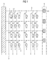
- Fig. 1 shows a schematic illustration of the memory device according to a first embodiment of the present invention.
- resistive memory cells 1 are arranged in an array in columns and rows.
- the resistive memory cell 1 comprises a resistive memory element 11 and a selection transistor 12.
- the resistive element 11 and the selection transistor 12 are arranged in a series connection between a bit line 3 and a reference electrode 4.
- every bit line 3 is assigned to one column, and every word line 2 is assigned to one row.
- the selection transistor 12 of each resistive memory cell 1 is further connected to a word line 2.
- An evaluation device 6, comprising evaluation units 61, is capable to evaluate the resistive state of a resistive memory cell 1 by applying to and/or measuring electrical signals between the corresponding bit line 3 and the reference electrode 4, upon addressing the respective word line 2.
- the memory device further comprises a charging device 5.
- the charging device 5 is connected to every bit line 3 of the memory device.
- the charging device 5 is capable to bring the bit lines 3 to a well defined potential. Since the bit lines 3 are subject to capacitive coupling among themselves and to other components of the memory device, the bit lines 3 may be charged to an uncontrolled potential when left electrically floating. Similar charging effects may occur through leakage currents between the bit lines and other components of the memory device.
- the evaluation device 6 When the reading device 6 is to carry out a reading operation, the evaluation device 6 will apply and/or measure an electrical signal between the reference electrode 4 and the respective bit line 3. In order to carry out a reliable reading operation and determine the resistive state of the resistive memory cell 1 correctly, the evaluation device 6 needs to bring the bit lines 3 to a well defined pre-reading potential first. This operation is necessary before every reading operation if the potential of the bit lines 3 is not controlled by other means. Said device will require a substantial delay before reading operations, and hence will possess only a limited overall performance.
- the memory device therefore further comprises a charging unit 5, which is able to bring the potential of the bit lines 3 to a well defined pre-reading potential, at a time when no reading operation is in progress.
- the charging device does not interfere with the reading device 6.
- the charging device 5 however, must not rely purely on the number of reading operations, since charging effects are independent of reading operations and in resistive memory devices, as in all modern random access memories, regular access to all the resistive memory cells is not given.
- the charging device will accordingly bring the potential of the bit lines 3 to a well defined pre-reading potential either after a certain time span has elapsed or a certain number of reading operations have been carried out. In both said cases, the charging device 5 must not charge the bit lines 3 when the evaluation device 6 is active, and a reading operation is in progress, since the charging of the charging device 5 then may influence the reading of the evaluation device 6.
- the inventive memory device relies on resistive memory cells 1 as its main component for storing information.
- Resistive memory cells 1 usually possess two or more distinguishable resistive states, to which two or more logical states correspond.
- the resistive memory cell 1 may be brought to a high and to a low resistive state, these two resistive states corresponding then to the two logical states "0" and "1". Since resistive memory media are capable to possess more than two distinguishable resistive states, the resistive memory cell 1 may also carry more than two logical states.
- resistive memory media examples include perovskite cells, phase change cells, and solid electrolyte cells (PMC, CB-RAM).
- PMC phase change cells
- PMC solid electrolyte cells
- metal ions are mobile within the solid electrolyte and hence can form conductive bridgings. These bridgings, comprising paths of metal ions or clusters thereof, may be formed and decomposed by respective electrical fields.
- the resistive memory cell 1 may comprise a resistive memory element 11 including Germanium-Selenide (GeSe, GeSe 2 ), Germanium-Sulfide (GeS, GeS 2 ), Germanium-Telluride (GeTe), Silicon-Selenide (SiSe), Silicon-Sulfide (SiS), Lead-Sulfide (PbS), Lead-Selenide (PbSe), Lead-Telluride (PbTe), Tin-Sulfide (SnS), Tin-Selenide (SnSe), Tin-Telluride (SnTe), Zinc-Sulfide (ZnS), Zinc-Selenide (ZnSe), Cadmium-Sulfide (CdS), Cadmium-Selenide (CdSe), Copper (Cu), Silver (Ag), Zinc (Zn), Lithium (Li), or Sodium (Na).
- Germanium-Selenide GeSe 2
- Fig. 2 shows a schematic illustration of the memory device according to a second embodiment of the present invention.
- the charging device 5 is embedded into the array of resistive memory cells 1, comprising one row of resistive memory cells 1.
- the resistive memory cells 1 of the charging device 5 are programmed, such that their resistive memory elements 51 are in a low resistive state.
- the selection transistors 12 of the resistive memory cells 1 of the charging device 5 are connected to a charging word line 52.
- the charging device 5 may be implemented by simply assigning one row of resistive memory cells 1 to the charging device 5. It is not necessary to integrate further or more complicated structures into the memory device to obtain the full functionality of the charging device 5.
- the functionality of the charging device 5 may be realized in a memory device with resistive memory cells even a posteriori if no charging device 5 has been initially designed. Which row of the array of resistive memory cells 1 is used for the charging device 5 is dependent on the actual layout of the memory device.
- one of the inner rows is assigned to the charging device 5. It may be preferable to assign one of the central inner rows of the array of resistive memory cells 1 to the charging device 5, since then the charging device 5 is coupled to the bit lines at a point where it intersects the bit lines 3 into more or less equal sections.
- the charging device 5 may be placed in the centre of the array is not mandatory, and according to the present invention any row of the array of resistive memory cells 1 may be assigned to the charging device 5.
- the reference electrodes 54 of the resistive memory cells 1 of the charging device 5 may be either coupled to the reference electrodes 4 of the remaining resistive memory cells 1, or to a second common reference electrode of the charging device 5. In the latter case, the charging device 5 is able to bring the bit lines 3 to a well defined pre-reading potential independently from the reference electrodes 4.
- the memory device further comprises a multiplexing device 7.
- the multiplexing device 7 pools two or more of the bit lines 3 to a set of bit lines, and connects one of these bit lines via selection transistors 72 to an evaluation device 6 with evaluation units 61, while disconnecting the remaining bit lines 3 of the set from the evaluation device 6. Since it is not required to access all bit lines 3 at the same time, the evaluation device may comprise a reduced number of evaluation units 61 for evaluating the resistive state of a resistive memory cell 1. This greatly simplifies the overall layout of the memory device.
- Evaluation of the resistive state of the resistive memory cells 1 is carried out via electrical signals between the respective bit line 3, which is selected by the multiplexing unit 7, and the reference electrode 4 upon addressing the respective word line 2. If a bit line 3 of a multiplexed set of bit lines is disconnected from the evaluation device 6 it may be electrically floating, giving rise to undesired charging effects of the respective bit line 3. According to the present invention, the charging device 5 may be employed here with its full advantage.
- Fig. 3 shows a schematic illustration of the memory device according to a third embodiment of the present invention.
- the charging device 5 is programmed such that the resistive memory cells 51 are all in a low resistive state, but at least one cell 53 is in a high resistive state.
- This differential programming is advantageous if the respective bit line 3 forms a short connection 8 with a word line 2.
- Short connections as for example the short connection 8 of the bit line 31 and the word line 21, do not cause too much loss of overall functionality and performance of the device.
- the bit line 31 may furthermore be replaced by a redundant spare bit line.
- the charging device 5 is programmed such that the respective resistive memory cell 53 is in a high resistive state. Upon addressing the charging word line 52, the faulty bit line is therefore not connected to the potential of the charging reference electrode.
- the charging device 5, comprising resistive memory cells 1 can be programmed to have low resistive memory cells 51 and high resistive memory cells 53 in a very flexible way after the actual faulty bit lines have been determined. Most preferably, the programming of the charging device 5 is carried out after a testing setup has determined all faulty bit lines.
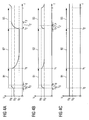
- Fig. 4A shows the bit line potential versus time according to prior art.
- the bit line potential V initially assumes an arbitrary value, for example a value between V 0 and V R .
- V R a reading potential
- bit line potential V may vary uncontrolled and may also, as an example, assume a maximum floating voltage V F . If a second reading operation 93 is to be carried out from a time t 2 onwards, the bit line potential V must be brought to V R before the actual reading operation may begin. Since the bit line potential V differs by
- the time spans T 0 and T 2 may vary in an uncontrolled way, and, as a consequence, the actual reading operation must be delayed by the longest possible time span T max before the resistive state of a resistive memory cell may be evaluated. This is very disadvantageous, since a substantial delay before every reading operation is required.
- Fig. 4B shows the bit line potential V versus time according to a fourth embodiment of the present invention.
- the bit line potential V is brought by a charging device 5 to a well defined pre-reading potential V 0 between two consecutive reading operations 91 and 93. Therefore the bit line potential V is kept at a well defined and controlled potential V 0 during periods 92 when no reading operation is effective.
- the time spans To and T 2 ' will be equal upon initialisation of every reading operation, as shown here in the case of the operations 91 and 93.
- the delay, which is required before every reading operation may be carried out, is therefore always the same (T 0 equals T 2 ' and can be tuned by the bias V 0 .
- T 0 equals T 2 ' and can be tuned by the bias V 0 .
- Fig. 4C shows the bit line potential V versus time according to a fifth embodiment of the present invention.
- the bit line potential V is kept by the charging device 5 at exactly or approximately the reading potential V R .
- the bit line potential V equals V R also in periods 92 when no reading operation is effective. A subsequent reading operation 93 may therefore commence immediately.
- the charging device 5 achieves a charging of the bit lines at the well defined pre-reading potential V R , via being coupled to a separate charging reference electrode.
Landscapes
- Chemical & Material Sciences (AREA)
- Engineering & Computer Science (AREA)
- Materials Engineering (AREA)
- Crystallography & Structural Chemistry (AREA)
- Semiconductor Memories (AREA)
Abstract
Description
- The present invention relates to a memory device comprising an array of resistive memory cells.
- Conventional electronic data memories, such as DRAM or Flash-RAM, are facing certain limitations as demands to modern data memories are steadily increasing. Above all, modern data memories must meet the requirement to combine a high density of information, fast memory access speed, and non-volatility. The latter non-volatility is increasingly important, since the memory content must be reliably maintained without supplying energy in - for example - mobile applications.
- Present electronic data memory concepts, such as the DRAM or the Flash-RAM, store the data in information units based on charged or uncharged capacitors. In the case of a DRAM, these capacitors must be refreshed continuously, as they are kept small in order to achieve a high density of information. Therefore, a separate electronic circuitry for constant reading and rewriting of the information content is necessary.
- Increasing the capacitors' size, as in a Flash-RAM, allows for the storage of information for a longer time span. The increased size of the data storage units however, then substantially limits integration and access speed. Additionally, higher operating voltages are required in a Flash-RAM, which further impose restrictions on integration and access speed.
- In order to combine non-volatility with fast access and high integration, alternatives to the DRAM and the Flash-RAM are subject to intense scientific and industrial research. Amongst others, the so-called resistive data storage media are most promising candidates for such a replacement and an enhancement of current technologies.
- Resistive data memories take advantage of various physical effects to cause a distinguishable and stable change of the electric resistance of special material systems. These systems include, for example, perovskite materials, phase change materials, and the so-called solid electrolytes. Memory cells employing solid electrolytes are also known as programmable metallization cells (PMC) or conductive brigding cells wherein an entire memory is referred to as CB-RAM. In a solid electrolyte a stable conductive bridging is formed by paths of metal ions being mobile in the solid electrolyte. These paths can be generated and decomposed by means of an electric field.
- Similar to a classical DRAM device, a memory device employing a resistive memory medium will comprise memory cells, which are arranged in an array of rows and columns. In this way billions of memory cells are integrated on a single chip. Since a large array of memory cells results in thousands of word and bit lines, it is furthermore desirable to pool a set of bit lines in order to simplify the external electronic circuitry. This pooling is usually carried out by means of a multiplexing unit, which connects one bit line out of a set of bit lines to an evaluation unit, while disconnecting the remaining bit lines.
- Although the integration of a multiplexing unit greatly simplifies the handling of large numbers of bit lines, only one bit line out of a set of bit lines is connected to an output port at a time. The remaining bit lines are disconnected from all external circuitry and hence may electrically float. This usually results in an undesired charging of the respective bit lines, which is mainly due to capacitive coupling between neighbouring bit lines and leakage currents.
- When a floating bit line is to be evaluated it must be first discharged and brought to a respective potential. Since the measured potential of a bit line eventually determines the logical state of the memory cell during a reading operation, compensation for parasitic charging effects of the bit lines must be suppressed. One method for eliminating these undesired charging effects is to connect a bit line to the evaluation unit by a multiplexing unit and to wait until all parasitic charge on the bit line has levelled trough the low impedance of the evaluation unit. This method requires additional time for every reading operation and hence strongly limits access speed and performance of the memory device.
- Taking the deficits of prior art, it is the object of the present invention to provide an improved memory device comprising an array of resistive memory cells. The object is met by a memory device according to claim. Preferred embodiments are disclosed in the dependent claims.
- According to the present invention a memory device is provided, wherein the memory device comprises an array of resistive memory cells, which are arranged in columns and rows. Said resistive memory cells are connected to a word line, to a bit line, and to a reference electrode, wherein the word lines are assigned to said rows and the bit lines are assigned to said columns. The resistive states of the resistive memory cells correspond to logical states of the resistive memory cells. The memory device further comprises an evaluation device for evaluating the resistive state of said resistive memory cells. The evaluation device is coupled to the bit lines and evaluates the resistive state during a reading operation, wherein the respective resistive memory cell is selected by addressing the word line to which the resistive memory cell is connected. The memory device further comprises a charging device which is coupled to the bit lines. The charging device is capable of charging the bit lines to a predetermined pre-reading bit line potential before carrying out a reading operation.
- During a reading operation the evaluation device evaluates the resistive state of a resistive memory cell. In general, the evaluation device is able to determine the resistive state by means of measuring an electric voltage or an electric current through the resistive memory cell. The resistive memory cells are connected to word lines, to bit lines, and to reference electrodes. A memory cell is selected via addressing the respective word line and connecting the respective bit line to the evaluation device. A current or a voltage may then be detected between the bit line and the reference electrode.
- When no reading operation is effective, the bit line may be disconnected from the evaluation device, and hence may electrically float, for the bit lines being subject to parasitic and uncontrolled charging effects. The bit line changes its potential due to the capacitive coupling and electrical leaks between adjacent bit lines or other components of the memory device. Therefore, the bit line may be at an uncontrolled potential at the time when the evaluation device starts evaluating the resistive state of a resistive memory cell, being connected to the respective bit line. In order to evaluate the state of the resistive memory cell in a reliable manner, the uncontrolled potential of the bit line must be brought to a well defined pre-reading potential before the reading operation may commence.
- Since the charging effects are uncontrolled and may furthermore vary over the period of operation, the evaluation device must wait for a sufficiently long time span to allow for a reliable reading operation. This is causing a substantial delay before every reading operation and strongly diminishes the overall memory device performance.
- According to the present invention the memory device comprises a charging device, which is coupled to the bit lines. This charging device is capable of charging the bit lines to a well defined potential at times when no reading operation is effective on the respective bit line. Since the charging device is coupled to all bit lines, it may connect said bit lines to a well defined pre-reading potential between reading operations. When the evaluation device is to carry out a reading operation, the charging device has kept the respective bit lines at the well defined potential, and the evaluation device may initiate the reading operation immediately. The inventive device therefore does not require a delay before reading operations, and hence possesses an increased overall device performance.
- According to an embodiment of the present invention the memory device further comprises a control device for controlling the charging device. The control device is suitable for controlling the charging device such that the charging device cycles the charging of the bit lines at dated periods of time. In this way, the charging device is controlled to bring the bit lines to a pre-reading bit line potential in well defined time intervals. The dated periods of time are chosen by the control device such that a charging operation does not interfere with a reading operation while a charging operation is carried out as often as required for a reliable operation of the evaluation device.
- According to another embodiment of the present invention the control device controls the charging device such that a charging operation of the bit lines is carried out at least every one thousand reading operations. In this way, it is assured that the bit lines are brought to the well defined pre-reading bit line potential at least every one thousand reading operations.
- According to a further embodiment of the present invention the pre-reading bit line potential to which the bit lines are brought by the charging device matches approximately the bit line potential during a reading operation. In order to determine the resistive state of a resistive memory cell an electric voltage is applied between the respective bit line and the reference electrode. This voltage corresponds to a bit line potential during a reading operation. If the charging device brings the bit lines during a charging operation to this bit line reading potential, the evaluation device may immediately initiate a reading operation. In this way, no delay occurs before a reading operation. According to a further embodiment of the present invention the absolute difference between the pre-reading bit line potential and the bit line potential during a reading operation is less than 2 Volts, preferably less than 1 Volt, and most preferably less than 0.1 Volts.
- According to a further embodiment of the present invention, the charging device is programmed such that a faulty bit line is excluded from the bit line charging operation. Although modern manufacturing processes for memory devices and other electronic integrated devices are highly sophisticated, structuring of various materials at the scale of only a few nanometres is often subject to deviations from the intentionally defined structures. Said deviations may result in local malfunctions of the device, such as electrical shorts or a high resistive impedance.
- A rather usual fault in the production of highly integrated memory devices is a short between a bit and a word line. According to this embodiment of the present invention, the charging device is programmed such that the faulty bit line, which is in undesired short contact with a word line, is excluded from the bit line charging operation. In this way, an interference between the bit line and the respective word line during a charging operation can be prevented.
- According to a next embodiment of the present invention the charging device comprises resistive memory cells, wherein the charging device comprises a resistive memory cell for each bit line. The resistive memory cells of the charging device are programmed such that they are in a low resistive state. The inventive device therefore is able to implement the charging device with a minimum of additional components or functional structures. Simply one row of resistive memory cells is assigned to the charging device which then can charge every bit line, since every bit line is connected to a memory cell of that row. The inventive device according to this embodiment of the present invention allows for a most simple implementation of the present invention. Either an additional row of resistive memory cells is realized within the array for being operated as the charging device, or one row of the array of resistive memory cells is assigned to the charging device and the respective word line of that row is addressed accordingly.
- According to a further embodiment of the present invention, the reference electrodes of the resistive memory cells of the charging device are coupled to a common charging reference electrode. According to this embodiment, the charging device is able to bring the bit lines to the potential of the common charging reference electrode, without interfering with the reference electrodes of the remaining resistive memory cells. Independently from the latter the charging device may bring the bit lines to an arbitrary well defined potential.
- According to a next embodiment of the present invention the resistive memory cells of the charging device are connected to a common charging word line. Addressing this common charging word line then activates the charging device, and all bit lines are brought to a well defined pre-reading potential according to the programming of the resistive memory cells of the charging device.
- According to a further embodiment of the present invention the resistive memory cells comprise a resistive memory element and a selection transistor. The resistive memory element and the selection transistor are arranged in a series connection between the corresponding bit line and the reference electrode. The selection transistor is further connected to the corresponding word line. With the arrangement according to this embodiment of the present invention, the resistive state of a resistive memory element, which are arranged in an array of rows and columns, can be easily accessed via addressing the corresponding word line and applying electrical signals between the corresponding bit line and the reference electrode.
- According to a further embodiment of the present invention, the resistive memory element comprises a solid electrolyte element, which preferably includes at least one of Germanium-Selenide (GeSe, GeSe2), Germanium-Sulfide (GeS, GeS2), Germanium-Telluride (GeTe), Silicon-Selenide (SiSe), Silicon-Sulfide (SiS), Lead-Sulfide (PbS), Lead-Selenide (PbSe), Lead-Telluride (PbTe), Tin-Sulfide (SnS), Tin-Selenide (SnSe), Tin-Telluride (SnTe), Zinc-Sulfide (ZnS), Zinc-Selenide (ZnSe), Cadmium-Sulfide (CdS), Cadmium-Selenide (CdSe), Copper (Cu), Silver (Ag), Zinc (Zn), Lithium (Li), or Sodium (Na). According to this embodiment of the present invention the resistive memory element may be manufactured from a solid electrolyte. Solid electrolytes represent a very promising and already rather sophisticated material system for resistive memory cells.
- According to a further embodiment of the present invention the memory device comprises a multiplexing device which is coupled to at least two bit lines. Said multiplexing device is able to connect one bit line to the evaluation device while disconnecting the remaining bit lines, which are coupled to the multiplexing device, from the evaluation device. According to this embodiment, a set of bit lines can be pooled and only one evaluation device is necessary for more than one bit line. Since not all bit lines have to be accessed simultaneously, the use of a multiplexing device greatly simplifies the device layout and strongly reduces the number of active components, which have to be integrated in the memory device.
- These and other objects and features of the present invention will become clear from the following description taken in conjunction with the accompanying drawings in which
- Fig. 1 shows a schematic view of the memory device, according to a first embodiment of the present invention;
- Fig. 2 shows a schematic view of the memory device, according to a second embodiment of the present invention;
- Fig. 3 shows a schematic view of the memory device, according to a third embodiment of the present invention;
- Fig. 4A shows the bit line potential versus time according to prior art;
- Fig. 4B shows the bit line potential versus time, according to a fourth embodiment of the present invention; and
- Fig. 4C shows the bit line potential versus time, according to a fifth embodiment of the present invention.
- Fig. 1 shows a schematic illustration of the memory device according to a first embodiment of the present invention. According to this embodiment,
resistive memory cells 1 are arranged in an array in columns and rows. Theresistive memory cell 1 comprises aresistive memory element 11 and aselection transistor 12. Theresistive element 11 and theselection transistor 12 are arranged in a series connection between abit line 3 and a reference electrode 4. In general, everybit line 3 is assigned to one column, and everyword line 2 is assigned to one row. Theselection transistor 12 of eachresistive memory cell 1 is further connected to aword line 2. Anevaluation device 6, comprisingevaluation units 61, is capable to evaluate the resistive state of aresistive memory cell 1 by applying to and/or measuring electrical signals between thecorresponding bit line 3 and the reference electrode 4, upon addressing therespective word line 2. - According to this embodiment of the present invention, the memory device further comprises a
charging device 5. The chargingdevice 5 is connected to everybit line 3 of the memory device. The chargingdevice 5 is capable to bring thebit lines 3 to a well defined potential. Since thebit lines 3 are subject to capacitive coupling among themselves and to other components of the memory device, thebit lines 3 may be charged to an uncontrolled potential when left electrically floating. Similar charging effects may occur through leakage currents between the bit lines and other components of the memory device. - When the
reading device 6 is to carry out a reading operation, theevaluation device 6 will apply and/or measure an electrical signal between the reference electrode 4 and therespective bit line 3. In order to carry out a reliable reading operation and determine the resistive state of theresistive memory cell 1 correctly, theevaluation device 6 needs to bring thebit lines 3 to a well defined pre-reading potential first. This operation is necessary before every reading operation if the potential of thebit lines 3 is not controlled by other means. Said device will require a substantial delay before reading operations, and hence will possess only a limited overall performance. - According to this embodiment of the present invention, the memory device therefore further comprises a
charging unit 5, which is able to bring the potential of thebit lines 3 to a well defined pre-reading potential, at a time when no reading operation is in progress. In this way, the charging device does not interfere with thereading device 6. Furthermore, it might not be necessary to bring the bit lines to a well defined pre-reading potential before every reading operation. - Since charging effects occur in characteristic time spans in the range of milliseconds, and modern memory devices operate in the range of nanoseconds for accessing the memory content, it is sufficient for the
charging device 5 to bring the potential of thebit lines 3 to a well defined pre-reading potential only after every one thousand reading operations. In general, the maximum number Nmax of reading operations after a charging step is required, calculates from
- with the characteristic time Tch in which uncontrolled charging effects bring the bit lines to a critical potential, and the time Tro for a single reading operation.
- The charging
device 5 however, must not rely purely on the number of reading operations, since charging effects are independent of reading operations and in resistive memory devices, as in all modern random access memories, regular access to all the resistive memory cells is not given. Preferably, the charging device will accordingly bring the potential of thebit lines 3 to a well defined pre-reading potential either after a certain time span has elapsed or a certain number of reading operations have been carried out. In both said cases, the chargingdevice 5 must not charge thebit lines 3 when theevaluation device 6 is active, and a reading operation is in progress, since the charging of thecharging device 5 then may influence the reading of theevaluation device 6. - The inventive memory device relies on
resistive memory cells 1 as its main component for storing information.Resistive memory cells 1 usually possess two or more distinguishable resistive states, to which two or more logical states correspond. As an example, theresistive memory cell 1 may be brought to a high and to a low resistive state, these two resistive states corresponding then to the two logical states "0" and "1". Since resistive memory media are capable to possess more than two distinguishable resistive states, theresistive memory cell 1 may also carry more than two logical states. - Examples for resistive memory media are perovskite cells, phase change cells, and solid electrolyte cells (PMC, CB-RAM). The latter, which also represent the most promising material system, metal ions are mobile within the solid electrolyte and hence can form conductive bridgings. These bridgings, comprising paths of metal ions or clusters thereof, may be formed and decomposed by respective electrical fields. In the case of solid electrolytes the
resistive memory cell 1 may comprise aresistive memory element 11 including Germanium-Selenide (GeSe, GeSe2), Germanium-Sulfide (GeS, GeS2), Germanium-Telluride (GeTe), Silicon-Selenide (SiSe), Silicon-Sulfide (SiS), Lead-Sulfide (PbS), Lead-Selenide (PbSe), Lead-Telluride (PbTe), Tin-Sulfide (SnS), Tin-Selenide (SnSe), Tin-Telluride (SnTe), Zinc-Sulfide (ZnS), Zinc-Selenide (ZnSe), Cadmium-Sulfide (CdS), Cadmium-Selenide (CdSe), Copper (Cu), Silver (Ag), Zinc (Zn), Lithium (Li), or Sodium (Na). - Fig. 2 shows a schematic illustration of the memory device according to a second embodiment of the present invention. According to this embodiment, the charging
device 5 is embedded into the array ofresistive memory cells 1, comprising one row ofresistive memory cells 1. Theresistive memory cells 1 of thecharging device 5 are programmed, such that theirresistive memory elements 51 are in a low resistive state. Further, theselection transistors 12 of theresistive memory cells 1 of thecharging device 5 are connected to a chargingword line 52. - According to this embodiment of the present invention, the charging
device 5 may be implemented by simply assigning one row ofresistive memory cells 1 to thecharging device 5. It is not necessary to integrate further or more complicated structures into the memory device to obtain the full functionality of thecharging device 5. In particular the functionality of thecharging device 5 may be realized in a memory device with resistive memory cells even a posteriori if no chargingdevice 5 has been initially designed. Which row of the array ofresistive memory cells 1 is used for thecharging device 5 is dependent on the actual layout of the memory device. - As shown in this embodiment of the present invention, one of the inner rows is assigned to the
charging device 5. It may be preferable to assign one of the central inner rows of the array ofresistive memory cells 1 to thecharging device 5, since then thecharging device 5 is coupled to the bit lines at a point where it intersects thebit lines 3 into more or less equal sections. Although placing thecharging device 5 in the centre of the array is not mandatory, and according to the present invention any row of the array ofresistive memory cells 1 may be assigned to thecharging device 5. Furthermore, thereference electrodes 54 of theresistive memory cells 1 of thecharging device 5 may be either coupled to the reference electrodes 4 of the remainingresistive memory cells 1, or to a second common reference electrode of thecharging device 5. In the latter case, the chargingdevice 5 is able to bring thebit lines 3 to a well defined pre-reading potential independently from the reference electrodes 4. - According to this embodiment of the present invention, the memory device further comprises a
multiplexing device 7. Themultiplexing device 7 pools two or more of thebit lines 3 to a set of bit lines, and connects one of these bit lines via selection transistors 72 to anevaluation device 6 withevaluation units 61, while disconnecting the remainingbit lines 3 of the set from theevaluation device 6. Since it is not required to access allbit lines 3 at the same time, the evaluation device may comprise a reduced number ofevaluation units 61 for evaluating the resistive state of aresistive memory cell 1. This greatly simplifies the overall layout of the memory device. - Evaluation of the resistive state of the
resistive memory cells 1 is carried out via electrical signals between therespective bit line 3, which is selected by themultiplexing unit 7, and the reference electrode 4 upon addressing therespective word line 2. If abit line 3 of a multiplexed set of bit lines is disconnected from theevaluation device 6 it may be electrically floating, giving rise to undesired charging effects of therespective bit line 3. According to the present invention, the chargingdevice 5 may be employed here with its full advantage. - Fig. 3 shows a schematic illustration of the memory device according to a third embodiment of the present invention. According to this embodiment, the charging
device 5 is programmed such that theresistive memory cells 51 are all in a low resistive state, but at least onecell 53 is in a high resistive state. This differential programming is advantageous if therespective bit line 3 forms a short connection 8 with aword line 2. - During manufacturing of modern and highly integrated memory devices, irregularities and deviations from the originally intended lithography rather often occur. Since modern devices are highly integrated, these irregularities and deviations can be easily corrected via excluding faulty parts and replacing their respective function by redundantly integrated components. Short connections, as for example the short connection 8 of the
bit line 31 and theword line 21, do not cause too much loss of overall functionality and performance of the device. In the case of the short 8, the column ofresistive memory cells 1 which are coupled to thebit line 31 which is in the undesired short connection 8 with theword line 21, is simply disabled. Due to the very high dimensions of modern memory arrays, the disabling of a single row or a single column does not reduce the device functionality substantially. Thebit line 31 may furthermore be replaced by a redundant spare bit line. - In order to exclude a faulty bit line also from charging, the charging
device 5 is programmed such that the respectiveresistive memory cell 53 is in a high resistive state. Upon addressing the chargingword line 52, the faulty bit line is therefore not connected to the potential of the charging reference electrode. A further advantage of the present invention is that thecharging device 5, comprisingresistive memory cells 1, can be programmed to have lowresistive memory cells 51 and highresistive memory cells 53 in a very flexible way after the actual faulty bit lines have been determined. Most preferably, the programming of thecharging device 5 is carried out after a testing setup has determined all faulty bit lines. - Fig. 4A shows the bit line potential versus time according to prior art. The bit line potential V initially assumes an arbitrary value, for example a value between V0 and VR. During a
first reading operation 91 the bit line potential V has to be brought to a reading potential VR. Due to an inherent and a parasitic capacitance of the bit line, this will take a time To from to to to'. Once the bit line potential V has reached the reading potential VR the actual reading operation may commence and is carried out in the remainder of theoperation 91. Thisoperation 91 ends at a time t1. - During a
period 92, ranging from t1 to t2, the bit line is not accessed. Due to leakages toward neighbouring components of the memory device and capacitive coupling, the bit line potential V may vary uncontrolled and may also, as an example, assume a maximum floating voltage VF. If asecond reading operation 93 is to be carried out from a time t2 onwards, the bit line potential V must be brought to VR before the actual reading operation may begin. Since the bit line potential V differs by |VF - VR|, it will take a longer time span T2 from t2 to t2', to bring the bit line potential V to the required reading potential VR. As can be seen from this example, the time spans T0 and T2 may vary in an uncontrolled way, and, as a consequence, the actual reading operation must be delayed by the longest possible time span Tmax before the resistive state of a resistive memory cell may be evaluated. This is very disadvantageous, since a substantial delay before every reading operation is required. - Fig. 4B shows the bit line potential V versus time according to a fourth embodiment of the present invention. According to this embodiment, the bit line potential V is brought by a
charging device 5 to a well defined pre-reading potential V0 between twoconsecutive reading operations periods 92 when no reading operation is effective. As a consequence, the time spans To and T2' will be equal upon initialisation of every reading operation, as shown here in the case of theoperations idle periods 92, the delay is substantially reduced and the overall performance of the memory device is strongly enhanced in contrast to prior art, as for example shown in Fig. 4A. - Fig. 4C shows the bit line potential V versus time according to a fifth embodiment of the present invention. According to this embodiment, the bit line potential V is kept by the charging
device 5 at exactly or approximately the reading potential VR. In this way, the bit line potential V equals VR also inperiods 92 when no reading operation is effective. Asubsequent reading operation 93 may therefore commence immediately. Most preferably thecharging device 5 achieves a charging of the bit lines at the well defined pre-reading potential VR, via being coupled to a separate charging reference electrode.
Claims (14)
- Memory device comprising an array of resistive memory cells (1), the resistive memory cells (1) being arranged in columns and rows,
said resistive memory cells (1) each being connected to a word line (2), to a bit line (3), and to a reference electrode (4), said word lines (2) being assigned to said rows and said bit lines (3) being assigned to said columns, wherein the resistive state of the resistive memory cells (1) corresponds to a logical state of the resistive memory cells (1),
the memory device further comprising an evaluation device (6) being coupled to the bit lines (3) for evaluating the resistive state of at least one of the resistive memory cells (1) during a reading operation, the respective resistive memory cell (1) being selected by addressing the word line (2) to which the resistive memory cell (1) is connected,
characterised by
a charging device (5) being coupled to the bit lines (3), said charging device (5) being capable of charging the bit lines (3) to a pre-determined pre-reading bit line potential before carrying out a reading operation. - Memory device as claimed in claim 1, characterised by a control device for controlling the charging device (5), said control device being suitable for controlling the charging device (5) such that the charging device (5) cycles the charging of the bit lines (3) to said pre-reading bit line potential at dated periods of time.
- Memory device as claimed in claim 2, characterised in that the control device controls the charging device (5) such that the charging device (5) charges the bit lines (3) to a pre-reading bit line potential after at least every 1000th reading operation.
- Memory device as claimed in one of the claims 1 to 3, characterised in that the pre-reading bit line potential approximately matches the bit line potential during a reading operation.
- Memory device as claimed in one of the claims 1 to 3, characterised in that the absolute difference between the pre-reading bit line potential and the bit line potential during a reading operation is less than 2 Volt.
- Memory device as claimed in one of the claims 1 to 3, characterised in that the absolute difference between the pre-reading bit line potential and the bit line potential during a reading operation is less than 1 Volt.
- Memory device as claimed in one of the claims 1 to 3, characterised in that the absolute difference between the pre-reading bit line potential and the bit line potential during the reading operation is less than 0.1 Volt.
- Memory device as claimed in one of the claims 1 to 7, characterised in that in case of a faulty bit line the charging device (5) is programmed such that the faulty bit line is excluded from the bit line charging operation.
- Memory device as claimed in one of the claims 1 to 8, characterised in that the charging device (5) comprises a resistive memory cell (1) for each bit line, said resistive memory cells (1) of the charging device (5) being programmed such that they are in a low resistive state.
- Memory device as claimed in claim 9, characterised in that the reference electrodes (54) of the resistive memory cells (1) of the charging device (5) are coupled to a common charging reference electrode.
- Memory device as claimed in claim 9 or 10, characterised in that the resistive memory cells (1) of the charging device are connected to a common charging word line (52).
- Memory device as claimed in one of the claims 9 to 11, characterised in that the resistive memory cells (1) comprise a resistive memory element (11) and a selection transistor (12) arranged in a series connection between the corresponding bit line (3) and the reference electrode (4, 54), said selection transistor (12) being further connected to the corresponding word line (2, 52).
- Memory device as claimed in claim 12, characterised in that the resistive memory element (11, 51, 53) comprises a solid electrolyte element, preferably including at least one of:- Germanium-Selenide (GeSe, GeSe2)- Germanium-Sulfide (GeS, GeS2)- Germanium-Telluride (GeTe)- Silicon-Selenide (SiSe)- Silicon-Sulfide (SiS)- Lead-Sulfide (PbS)- Lead-Selenide (PbSe)- Lead-Telluride (PbTe)- Tin-Sulfide (SnS)- Tin-Selenide (SnSe)- Tin-Telluride (SnTe)- Zinc-Sulfide (ZnS)- Zinc-Selenide (ZnSe)- Cadmium-Sulfide (CdS)- Cadmium-Selenide (CdSe)- Copper (Cu)- Silver (Ag)- Zinc (Zn)- Lithium (Li)- Sodium (Na)
- Memory device as claimed in one of the claims 1 to 13, characterised by a multiplexing device (7) coupled to at least two bit lines (3) to connect one of said bit lines (3) to the evaluation device (6).
Priority Applications (2)
| Application Number | Priority Date | Filing Date | Title |
|---|---|---|---|
| DE200560013964 DE602005013964D1 (en) | 2005-09-29 | 2005-09-29 | Memory with resistance memory cell matrix and bit line charging |
| EP05021351A EP1770709B1 (en) | 2005-09-29 | 2005-09-29 | Memory device comprising an array of resistive memory cells with bit lines precharging |
Applications Claiming Priority (1)
| Application Number | Priority Date | Filing Date | Title |
|---|---|---|---|
| EP05021351A EP1770709B1 (en) | 2005-09-29 | 2005-09-29 | Memory device comprising an array of resistive memory cells with bit lines precharging |
Publications (2)
| Publication Number | Publication Date |
|---|---|
| EP1770709A1 true EP1770709A1 (en) | 2007-04-04 |
| EP1770709B1 EP1770709B1 (en) | 2010-07-07 |
Family
ID=35810248
Family Applications (1)
| Application Number | Title | Priority Date | Filing Date |
|---|---|---|---|
| EP05021351A Expired - Lifetime EP1770709B1 (en) | 2005-09-29 | 2005-09-29 | Memory device comprising an array of resistive memory cells with bit lines precharging |
Country Status (2)
| Country | Link |
|---|---|
| EP (1) | EP1770709B1 (en) |
| DE (1) | DE602005013964D1 (en) |
Citations (6)
| Publication number | Priority date | Publication date | Assignee | Title |
|---|---|---|---|---|
| US5390150A (en) * | 1992-04-24 | 1995-02-14 | Samsung Electronics Co., Ltd. | Semiconductor memory device with redundancy structure suppressing power consumption |
| US6418049B1 (en) * | 1997-12-04 | 2002-07-09 | Arizona Board Of Regents | Programmable sub-surface aggregating metallization structure and method of making same |
| US20020154531A1 (en) * | 1999-12-16 | 2002-10-24 | Tyler Lowrey | Programmable resistance memory array |
| US20030123281A1 (en) * | 2001-12-28 | 2003-07-03 | Yoshihisa Iwata | Magnetic random access memory |
| US20030128612A1 (en) * | 2002-01-04 | 2003-07-10 | John Moore | PCRAM rewrite prevention |
| US20040184331A1 (en) * | 2002-02-01 | 2004-09-23 | Satoru Hanzawa | Storage device |
Family Cites Families (2)
| Publication number | Priority date | Publication date | Assignee | Title |
|---|---|---|---|---|
| EP0121394B1 (en) * | 1983-03-28 | 1991-10-23 | Fujitsu Limited | Static semiconductor memory device incorporating redundancy memory cells |
| US6594192B1 (en) * | 2000-08-31 | 2003-07-15 | Stmicroelectronics, Inc. | Integrated volatile and non-volatile memory |
-
2005
- 2005-09-29 DE DE200560013964 patent/DE602005013964D1/en not_active Expired - Lifetime
- 2005-09-29 EP EP05021351A patent/EP1770709B1/en not_active Expired - Lifetime
Patent Citations (6)
| Publication number | Priority date | Publication date | Assignee | Title |
|---|---|---|---|---|
| US5390150A (en) * | 1992-04-24 | 1995-02-14 | Samsung Electronics Co., Ltd. | Semiconductor memory device with redundancy structure suppressing power consumption |
| US6418049B1 (en) * | 1997-12-04 | 2002-07-09 | Arizona Board Of Regents | Programmable sub-surface aggregating metallization structure and method of making same |
| US20020154531A1 (en) * | 1999-12-16 | 2002-10-24 | Tyler Lowrey | Programmable resistance memory array |
| US20030123281A1 (en) * | 2001-12-28 | 2003-07-03 | Yoshihisa Iwata | Magnetic random access memory |
| US20030128612A1 (en) * | 2002-01-04 | 2003-07-10 | John Moore | PCRAM rewrite prevention |
| US20040184331A1 (en) * | 2002-02-01 | 2004-09-23 | Satoru Hanzawa | Storage device |
Also Published As
| Publication number | Publication date |
|---|---|
| DE602005013964D1 (en) | 2009-05-28 |
| EP1770709B1 (en) | 2010-07-07 |
Similar Documents
| Publication | Publication Date | Title |
|---|---|---|
| US7251152B2 (en) | Memory circuit having memory cells which have a resistance memory element | |
| TWI480873B (en) | Non-volatile semiconductor memory device | |
| KR100263084B1 (en) | Dynamic Adjustment of Voltage Reference for Ferroelectric Circuits | |
| US20080043521A1 (en) | Method of determining a memory state of a resistive memory cell and device measuring the memory state of a resistive memory cell | |
| KR100626508B1 (en) | Programmable Conductor Random Access Memory and Its Sensing Method | |
| US5737260A (en) | Dual mode ferroelectric memory reference scheme | |
| JP6748792B2 (en) | 2T1C ferroelectric random access memory cell | |
| US7372716B2 (en) | Memory having CBRAM memory cells and method | |
| US7400521B1 (en) | Integrated circuit, memory chip and method of evaluating a memory state of a resistive memory cell | |
| US11688449B2 (en) | Memory management for charge leakage in a memory device | |
| KR20110094240A (en) | Nonvolatile Semiconductor Memory Devices | |
| CN110827877A (en) | Access scheme for access line failures in memory devices | |
| US9036401B2 (en) | Memory cell operation | |
| US20260057922A1 (en) | Word line voltage control for reduced voltage disturbance during memory operations | |
| US7257013B2 (en) | Method for writing data into a memory cell of a conductive bridging random access memory, memory circuit and CBRAM memory circuit | |
| US8872542B2 (en) | Semiconductor device and semiconductor device control method | |
| US7154768B2 (en) | Non-destructive readout of ferroelectric memories | |
| CN115206378B (en) | System and method for reducing the impact of short bits in a phase change memory array | |
| US7254073B2 (en) | Memory device having an array of resistive memory cells | |
| US7106641B2 (en) | Dynamic semiconductor memory device | |
| EP1770709B1 (en) | Memory device comprising an array of resistive memory cells with bit lines precharging | |
| US20090257264A1 (en) | Memory and method of evaluating a memory state of a resistive memory cell | |
| WO1998033184A1 (en) | Reference cell system for memories based on ferroelectric memory cells | |
| EP1763038A1 (en) | Method for writing data into a memory cell of a conductive bridging random access memory, memory circuit and CBRAM memory circuit | |
| US20090122586A1 (en) | Method and apparatus for an integrated circuit with programmable memory cells, data system |
Legal Events
| Date | Code | Title | Description |
|---|---|---|---|
| PUAI | Public reference made under article 153(3) epc to a published international application that has entered the european phase |
Free format text: ORIGINAL CODE: 0009012 |
|
| AK | Designated contracting states |
Kind code of ref document: A1 Designated state(s): AT BE BG CH CY CZ DE DK EE ES FI FR GB GR HU IE IS IT LI LT LU LV MC NL PL PT RO SE SI SK TR |
|
| AX | Request for extension of the european patent |
Extension state: AL BA HR MK YU |
|
| 17P | Request for examination filed |
Effective date: 20070407 |
|
| RAP1 | Party data changed (applicant data changed or rights of an application transferred) |
Owner name: QIMONDA AG |
|
| 17Q | First examination report despatched |
Effective date: 20070604 |
|
| AKX | Designation fees paid |
Designated state(s): DE FR GB |
|
| GRAP | Despatch of communication of intention to grant a patent |
Free format text: ORIGINAL CODE: EPIDOSNIGR1 |
|
| GRAS | Grant fee paid |
Free format text: ORIGINAL CODE: EPIDOSNIGR3 |
|
| GRAA | (expected) grant |
Free format text: ORIGINAL CODE: 0009210 |
|
| AK | Designated contracting states |
Kind code of ref document: B1 Designated state(s): DE FR GB |
|
| REG | Reference to a national code |
Ref country code: GB Ref legal event code: FG4D |
|
| 29U | Proceedings interrupted after grant according to rule 142 epc |
Effective date: 20090401 |
|
| REF | Corresponds to: |
Ref document number: 602005013964 Country of ref document: DE Date of ref document: 20090528 Kind code of ref document: P |
|
| PUAC | Information related to the publication of a b1 document modified or deleted |
Free format text: ORIGINAL CODE: 0009299EPPU |
|
| 29W | Proceedings resumed after grant [after interruption of proceedings according to rule 142 epc] |
Effective date: 20091123 |
|
| DB1 | Publication of patent cancelled | ||
| GRAA | (expected) grant |
Free format text: ORIGINAL CODE: 0009210 |
|
| AK | Designated contracting states |
Kind code of ref document: B1 Designated state(s): DE FR GB |
|
| REG | Reference to a national code |
Ref country code: GB Ref legal event code: FG4D |
|
| PLBE | No opposition filed within time limit |
Free format text: ORIGINAL CODE: 0009261 |
|
| STAA | Information on the status of an ep patent application or granted ep patent |
Free format text: STATUS: NO OPPOSITION FILED WITHIN TIME LIMIT |
|
| 26N | No opposition filed |
Effective date: 20110408 |
|
| GBPC | Gb: european patent ceased through non-payment of renewal fee |
Effective date: 20101007 |
|
| REG | Reference to a national code |
Ref country code: DE Ref legal event code: R097 Ref document number: 602005013964 Country of ref document: DE Effective date: 20110408 |
|
| PG25 | Lapsed in a contracting state [announced via postgrant information from national office to epo] |
Ref country code: GB Free format text: LAPSE BECAUSE OF NON-PAYMENT OF DUE FEES Effective date: 20101007 |
|
| REG | Reference to a national code |
Ref country code: DE Ref legal event code: R081 Ref document number: 602005013964 Country of ref document: DE Owner name: INFINEON TECHNOLOGIES AG, DE Free format text: FORMER OWNER: QIMONDA AG, 81739 MUENCHEN, DE Ref country code: DE Ref legal event code: R081 Ref document number: 602005013964 Country of ref document: DE Owner name: POLARIS INNOVATIONS LTD., IE Free format text: FORMER OWNER: QIMONDA AG, 81739 MUENCHEN, DE |
|
| REG | Reference to a national code |
Ref country code: DE Ref legal event code: R081 Ref document number: 602005013964 Country of ref document: DE Owner name: POLARIS INNOVATIONS LTD., IE Free format text: FORMER OWNER: INFINEON TECHNOLOGIES AG, 85579 NEUBIBERG, DE |
|
| PG25 | Lapsed in a contracting state [announced via postgrant information from national office to epo] |
Ref country code: FR Free format text: LAPSE BECAUSE OF NON-PAYMENT OF DUE FEES Effective date: 20100707 |
|
| PGFP | Annual fee paid to national office [announced via postgrant information from national office to epo] |
Ref country code: DE Payment date: 20160920 Year of fee payment: 12 |
|
| REG | Reference to a national code |
Ref country code: FR Ref legal event code: ST Effective date: 20170428 |
|
| PG25 | Lapsed in a contracting state [announced via postgrant information from national office to epo] |
Ref country code: FR Free format text: LAPSE BECAUSE OF NON-PAYMENT OF DUE FEES Effective date: 20100930 |
|
| REG | Reference to a national code |
Ref country code: DE Ref legal event code: R119 Ref document number: 602005013964 Country of ref document: DE |
|
| PG25 | Lapsed in a contracting state [announced via postgrant information from national office to epo] |
Ref country code: DE Free format text: LAPSE BECAUSE OF NON-PAYMENT OF DUE FEES Effective date: 20180404 |