EP1770439A1 - Alternating phase shift mask - Google Patents
Alternating phase shift mask Download PDFInfo
- Publication number
- EP1770439A1 EP1770439A1 EP05447222A EP05447222A EP1770439A1 EP 1770439 A1 EP1770439 A1 EP 1770439A1 EP 05447222 A EP05447222 A EP 05447222A EP 05447222 A EP05447222 A EP 05447222A EP 1770439 A1 EP1770439 A1 EP 1770439A1
- Authority
- EP
- European Patent Office
- Prior art keywords
- mask
- phase shift
- parameters
- shift mask
- focus
- Prior art date
- Legal status (The legal status is an assumption and is not a legal conclusion. Google has not performed a legal analysis and makes no representation as to the accuracy of the status listed.)
- Granted
Links
- 230000010363 phase shift Effects 0.000 title claims abstract description 136
- 238000000034 method Methods 0.000 claims abstract description 87
- 238000012545 processing Methods 0.000 claims abstract description 64
- 238000005286 illumination Methods 0.000 claims description 56
- 238000006073 displacement reaction Methods 0.000 claims description 33
- 230000000903 blocking effect Effects 0.000 claims description 30
- 238000005530 etching Methods 0.000 claims description 28
- 239000000758 substrate Substances 0.000 claims description 23
- 238000004590 computer program Methods 0.000 claims description 8
- 239000011159 matrix material Substances 0.000 claims description 5
- 230000005540 biological transmission Effects 0.000 claims description 3
- 238000013500 data storage Methods 0.000 claims description 2
- 238000011156 evaluation Methods 0.000 abstract description 8
- 230000008569 process Effects 0.000 description 27
- 239000011295 pitch Substances 0.000 description 24
- 230000006870 function Effects 0.000 description 17
- 230000006399 behavior Effects 0.000 description 16
- 230000008901 benefit Effects 0.000 description 12
- VYZAMTAEIAYCRO-UHFFFAOYSA-N Chromium Chemical compound [Cr] VYZAMTAEIAYCRO-UHFFFAOYSA-N 0.000 description 10
- 230000009467 reduction Effects 0.000 description 10
- 238000004519 manufacturing process Methods 0.000 description 9
- 230000001419 dependent effect Effects 0.000 description 7
- 238000013461 design Methods 0.000 description 7
- 239000000463 material Substances 0.000 description 7
- 229910052804 chromium Inorganic materials 0.000 description 5
- 239000011651 chromium Substances 0.000 description 5
- 238000010276 construction Methods 0.000 description 5
- 238000003384 imaging method Methods 0.000 description 5
- 230000003287 optical effect Effects 0.000 description 4
- 238000002474 experimental method Methods 0.000 description 3
- 238000001459 lithography Methods 0.000 description 3
- 239000012780 transparent material Substances 0.000 description 3
- 230000015572 biosynthetic process Effects 0.000 description 2
- 230000001066 destructive effect Effects 0.000 description 2
- 230000000694 effects Effects 0.000 description 2
- 238000004088 simulation Methods 0.000 description 2
- 238000012876 topography Methods 0.000 description 2
- 238000000149 argon plasma sintering Methods 0.000 description 1
- 238000013528 artificial neural network Methods 0.000 description 1
- 230000002238 attenuated effect Effects 0.000 description 1
- 238000004364 calculation method Methods 0.000 description 1
- 238000012937 correction Methods 0.000 description 1
- 230000008021 deposition Effects 0.000 description 1
- 230000005288 electromagnetic effect Effects 0.000 description 1
- 238000012854 evaluation process Methods 0.000 description 1
- 238000000605 extraction Methods 0.000 description 1
- 239000011521 glass Substances 0.000 description 1
- 238000012986 modification Methods 0.000 description 1
- 230000004048 modification Effects 0.000 description 1
- 238000005457 optimization Methods 0.000 description 1
- 238000000059 patterning Methods 0.000 description 1
- 229920002120 photoresistant polymer Polymers 0.000 description 1
- 239000011312 pitch solution Substances 0.000 description 1
- 239000010453 quartz Substances 0.000 description 1
- 230000035945 sensitivity Effects 0.000 description 1
- VYPSYNLAJGMNEJ-UHFFFAOYSA-N silicon dioxide Inorganic materials O=[Si]=O VYPSYNLAJGMNEJ-UHFFFAOYSA-N 0.000 description 1
- 238000003860 storage Methods 0.000 description 1
Images


Classifications
-
- G—PHYSICS
- G03—PHOTOGRAPHY; CINEMATOGRAPHY; ANALOGOUS TECHNIQUES USING WAVES OTHER THAN OPTICAL WAVES; ELECTROGRAPHY; HOLOGRAPHY
- G03F—PHOTOMECHANICAL PRODUCTION OF TEXTURED OR PATTERNED SURFACES, e.g. FOR PRINTING, FOR PROCESSING OF SEMICONDUCTOR DEVICES; MATERIALS THEREFOR; ORIGINALS THEREFOR; APPARATUS SPECIALLY ADAPTED THEREFOR
- G03F1/00—Originals for photomechanical production of textured or patterned surfaces, e.g., masks, photo-masks, reticles; Mask blanks or pellicles therefor; Containers specially adapted therefor; Preparation thereof
- G03F1/26—Phase shift masks [PSM]; PSM blanks; Preparation thereof
- G03F1/30—Alternating PSM, e.g. Levenson-Shibuya PSM; Preparation thereof
Definitions
- the present invention relates to methods and systems for lithographic processing of a device. More particularly, the present invention relates to lithographic alternating phase shift masks, methods of making them and methods of using lithographic alternating phase shift masks.
- Lithographic processing is one of the key features in the manufacturing of today's circuits and integrated components.
- the quality of the lithographic processing is strongly dependent on the lithographic system and the mask used.
- Different types of lithographic masks are known such as binary masks, like chrome on glass masks and phase shift masks, such as e.g. alternating phase shift masks and attenuated phase shift masks.
- Alternating phase shift masks are masks wherein transmitting areas are used having a 180° phase difference with other transmitting areas of the mask. A feature on mask thereby is always surrounded by transmitting regions of different phase. The occurrence of the phase difference leads to destructive interference, resulting in a sharp dark image.
- a disadvantage of the use of alternating phase shift masks is the occurrence of image imbalance, which is intrinsically related to alternating phase shift mask imaging, leading to focus-dependent feature shifts.
- An appropriate compensation for the induced focus-dependent feature shifts, such as e.g. line displacements, is needed in order to fully exploit the advantages of alternating phase shift mask imaging.
- Feature shift can originate from light scattering in the trenches of the alternating phase shift mask.
- An alternative source for image imbalance is the occurrence of a phase error, e.g. by a wrong effective phase shift of the light in the trenches. This might be caused by a mask fabrication error but also can be due to an intrinsic 3D effect due to the small feature sizes involved. Even a perfect mask, such as e.g. a simulated mask, can suffer from these intrinsic 3D effects, and thus from this type of image imbalance.
- Fig. 1a illustrates a mask 10 with compensation by undercut of the blocking region, indicated by the dashed region, adjacent a ⁇ -phase region, i.e. providing some undercut of the light-blocking layer, e.g. chrome layer.
- Fig. 1b shows a mask 20 with compensation by double trenching whereby a shallow trench is provided at the 0 phase region at the left of the blocking region, indicated by the dashed region.
- Fig. 1c shows a mask 30 with compensation by trench-space biasing for the ⁇ phase region at the right of the blocking region indicated by the dashed region.
- Providing undercut, using double trenching, using double patterning or applying side-wall chrome alternating aperture mask features may allow reduction of image imbalance caused by scattering.
- double exposure may be performed or additional measures can be taken when manufacturing the mask, such as e.g. an etch stop layer may be provided to avoid micro-loading.
- phase shift masks It is an object of the present invention to provide improved phase shift masks, methods of manufacturing such improved phase shift masks and methods for using such improved phase shift masks. It is an advantage of embodiments of the present invention to provide phase shift masks allowing reduction of image imbalance during lithographic processing of a device.
- the present invention relates to a method for making a phase shift mask in or on a substrate, said phase shift mask being suitable for lithographic processing of a device using a predetermined illumination dose.
- the method comprises etching said substrate according to mask parameters, wherein said mask parameters are selected taking into account said illumination dose.
- Selecting mask parameters may be selecting values for said mask parameters.
- Etching said substrate may comprise forming a trench in said substrate, wherein said mask parameters may comprise at least an etching depth for a trench. In other words, a value for said etching depth, corresponding with the trench depth, may be selected taking into account said illumination dose.
- Said mask parameters also may comprise a trench bias and a light blocking part bias, e.g. a Chrome width. In other words the light blocking part bias and/or the trench bias may be determined taking into account the illumination dose.
- the invention also relates to a method of designing a phase shift mask suitable for lithographic processing of a device using a predetermined illumination dose.
- the method comprises selecting a set of mask parameters taking into account said illumination dose.
- Said selecting a set of mask parameters may comprise selecting a plurality of sets of mask parameters suitable for using said phase shift mask substantially in focus, and selecting from said plurality of sets of mask parameters at least one set of mask parameters suitable for using said phase shift mask with said illumination dose in a predetermined out of focus range.
- said mask may comprise at least a trench and light blocking parts and said mask parameters may comprise at least a trench bias, a light blocking part bias and an etching depth of said trench, said mask being suitable for printing features on a device.
- Selecting a plurality of sets of mask parameters suitable for using said phase shift mask substantially in focus may comprise adjusting the light blocking part bias to correct a feature size and adjusting the trench bias to correct a feature position.
- Said trench bias and said light blocking part bias may be optimised for a predetermined range of doses, a predetermined range of etching depths and/or a predetermined range of pitches.
- Said mask may comprise at least a trench and said mask parameters may comprise at least an etching depth of said trench, whereby said selecting at least one set of mask parameters suitable for using said phase shift mask with said illumination dose in a predetermined out of focus range, may comprise selecting a set of mask parameters corresponding with a predetermined etching depth.
- Said selecting at least one set of mask parameters suitable for using said phase shift mask with said illumination dose in a predetermined out of focus range may comprise determining any of a focus-exposure matrix or an amount of feature displacement for a feature printable using said mask for said plurality of sets of mask parameters, and evaluating said focus exposure matrix or said amount of feature displacement for a feature printable using said mask.
- Said method may comprise evaluating a focus-exposure window for a feature printable using said mask, wherein said focus-exposure window is determined by a part of focus-exposure windows for at least two edges of said feature printable using said mask.
- the focus-exposure window used for evaluating is determined by the overlapping part of the focus-exposure windows for the edges of the feature printable using said mask.
- the invention also relates to a method for performing lithographic processing of a device, the method comprising using a phase shift mask and using an illumination dose, wherein one of said phase shift mask and said illumination dose are selected as a function of the other.
- said phase shift mask may be made according to any of the methods for making a phase shift mask as described above or said phase shift mask may be made according to any of the methods for designing as described above
- an illumination dose may be selected as function of mask parameters of said phase shift mask. Said selection may be performed as a function of a depth of a trench in said phase shift mask.
- the present invention furthermore relates to a phase shift mask suitable for lithographic processing of a device using a predetermined illumination dose, the phase shift mask comprising a substrate with at least one means for generating a phase shift, a geometric size of said means for generating a phase shift being determined taking into account said illumination dose.
- Said geometrical size may be e.g. a thickness of a phase shift film or a depth of a trench in a transparent material.
- Said geometrical size may e.g. be a width and/or a depth of a trench or a width of a light blocking part.
- the invention also relates to a computer program product for designing a phase shift mask according to a method for designing as described above. It furthermore relates to a machine readable data storage device storing such a computer program product, or to the transmission of such a computer program product over a local or wide area telecommunications network.
- teachings of the present invention permit the design of improved alternating phase shift masks resulting in improved lithographic processing.
- the present invention relates to an alternating phase shift mask, which can e.g. be used for lithographic processing of a device.
- the alternating phase shift mask of the present embodiment has mask parameters determined taking into account the threshold of illumination or the dose of illumination that will be used in lithographic processing for the alternating phase shift mask manufactured according to embodiments of the present invention.
- the mask typically will contain mask features such that it can be used for generation of a pattern on a device.
- An alternating phase shift mask typically comprises, in parts of the mask that are not blocking, means for generating a phase shift near the mask features such that, at such locations, destructive interference occurs and features can be imaged with a high contrast.
- the means for generating a phase shift may be any suitable type of means, such as e.g.
- a means for phase shifting comprising a phase shifting film or comprising a phase shifting substrate with regions having different optical thickness.
- the means for generating a phase shift may be a trench in a phase shifting substrate, which forms the basis of the mask.
- Alternating phase shift masks are known to generate image imbalance thus creating displacement of the printed features.
- image imbalance generates line displacement, as shown in Fig. 1d and Fig. 1e for line displacement generated by phase errors in the phase shift mask and for line displacement caused by trench bias differences respectively.
- FIG. 1d shows line displacements as function of the focus behaviour whereby curve 42 typically shows line displacement for a phase smaller than the optimum phase is present, curve 44 illustrates the line displacement when no phase error is made and curve 46 illustrates the line displacement when a phase larger than the optimum phase is present.
- Fig. 1e shows line displacements as function of the focus behaviour whereby curve 52 shows typically line displacement for a too small trench bias, curve 54 shows typically line displacement for a correct trench bias and curve 56 shows typically line displacement for a too large trench bias.
- the parameters involved may be the depth of a trench provided in a phase shifting substrate, the width of the trench, the shape of the trench, the thickness of a phase shifting film, the width of the phase shifting film, etc. It is to be noted that the amount of illumination may be expressed using parameters such as the dose of illumination or the threshold of the aerial image. Both parameters are related to each other by threshold ⁇ 1 dose .
- an alternating phase shift mask 100 is shown in Fig. 2, with a substrate 102, a patterned light blocking layer 104, such as e.g. a chromium layer, a first phase shift region 106 and a second phase shift region 108.
- the first phase shift region 106 is referred to as a 0 phase shift region, as it provides no other phase shift than the one provided by the full substrate thickness
- the second phase shift region 108 is referred to as a ⁇ phase shift region, as it provides a phase shift ⁇ with respect to light passing to the full substrate thickness.
- Such a ⁇ phase shift region is created by introducing a trench 110, such that the optical path length in the substrate 102 at the location of the trench 110 is substantially smaller.
- the etching depth d etch used for forming the trench 110 thus determines the phase shift that is provided.
- the alternating phase shift mask 100 may allow obtaining a reduction in image imbalance for a large process window and for a large number of pitches.
- the means for generating a phase shift furthermore may comprise a double trench, undercut or any other features for providing compensation for image imbalance, as known by the person skilled in the art.
- the mask 100 may comprise additional features that are typically used in lithographic processing; such as for example Optical Proximity Correction (OPC) features, as known by a person skilled in the art.
- OPC Optical Proximity Correction
- the present invention relates to a method for designing an alternating phase shift mask 100, whereby the amount of illumination, e.g. expressed by the dose of illumination or the threshold for illumination, used for illumination of the alternating phase shift mask 100 during its later use in lithographic processing is taken into account already during the design stage. More precisely, especially for reducing image imbalance in the through focus behaviour, taking into account the dose may lead to significant improvements.
- the lithographic process is sensitive to variations in the focus depth one should not only determine the dimensions of the features printed on a substrate at the optimal focus but also at focus settings which deviate from this optimal focus setting. The sensitivity of the lithographic process will depend on the mask parameters of the mask as manufactured as these parameters may deviate from the determined optimal mask parameters, e.g. phase error, trench bias error.
- An example of a method for designing 150 according to the present embodiment may comprise following standard and/or optional steps, as shown by way of illustration in Fig. 3.
- the initial mask settings are provided.
- the initial mask settings typically correspond with conventional mask settings used by a person skilled in the art for obtaining a mask allowing creation of a pattern on a device during lithographic processing. These conventional mask settings typically may comprise an initial etch depth d etch , an initial dose and typical pitches in agreement with the pattern to be made on the device during lithographic processing using the mask. Further settings of the mask, such as an initial bias for the light blocking material, such as e.g. an initial Chromium bias, and an initial trench bias may be selected.
- an initial bias for the light blocking material such as e.g. an initial Chromium bias
- an initial trench bias may be selected.
- allowable mask parameters are determined for best focus behaviour, whereby the allowable mask parameters are determined for a wide range of doses, i.e. for a wide range of thresholds for illumination that will be used during lithographic processing of a device with the mask 100. Determining allowable mask parameters may e.g. be performed using the following steps. A set of mask parameters may be selected, as shown in step 156. These parameters can be based on the initial mask parameters provided in the first step 152, whereby several parameters may be varied within predetermined ranges. In a decision step 158, it is checked whether the image imbalance at best focus is under control, i.e. whether the image imbalance is not too large. The amount of image imbalance that is allowed depends on the specific lithographic processing.
- the latter may e.g. comprise evaluating whether the printed feature is at the correct position and has the correct width/lateral dimensions. It may comprise evaluating the position of the edges of the features separately. If the image imbalance at best focus is sufficiently small, the set of parameters are evaluated as allowable, as shown in step 160. These parameters may e.g. be stored in a memory and/or these parameters may e.g. be outputted. If the image imbalance is not sufficiently controlled, the parameters may be adjusted, as shown in step 162, and new evaluation of the image imbalance may be made. Typical parameters that may be adjusted are the light blocking part bias, such as e.g. the chromium bias, in order to get the correct resist feature size, e.g.
- the light blocking part bias such as e.g. the chromium bias
- These parameters typically are evaluated for a setting of a dose in a predetermined range, an etching depth in a predetermined range and a pitch in a predetermined range. Such variation may be done systematically such that a whole parameter space is evaluated for predetermined ranges of each parameter. The evaluation preferably is done by simulating the obtained results for an alternating phase shift mask determined by the selected parameters and using the provided dose, although the latter in principle also could be determined through theoretical calculations or through experiments.
- a typical simulation engine that may be used is Prolith as available from KLA-Tencor, such as e.g. Protlith version 8.1 comprising the mask topography option. To determine the optimum mask parameters, rigorous simulation of the electromagnetic effects of light transmission through the mask topography may be used.
- the through focus behaviour is determined for the allowable mask parameters, as shown in step 164.
- the allowable mask parameters thereby typically may be allowable settings for the light blocking part bias and trench bias for a given dose, a given etching depth and a given pitch.
- Determining the through focus behaviour i.e. the behaviour for focus settings differing from the best focus, may comprise calculating a mask error enhancement factor, a focus - exposure matrix for the features provided on the mask, positional information of the features provided on the mask and a line displacement slope for different pitches as a function of the dose.
- studying the line displacement slope as a function of the dose may allow evaluation of the through focus behaviour.
- selection of the optimum etching depth taking into account the adequate dose is performed for the through focus behaviour, or selection of the optimum dose taking into account the adequate etching depth is performed for through focus behaviour, whereby the selection is made from the sets of allowable mask parameters.
- the latter typically results in optimum mask parameters for both best focus and through focus behaviour.
- Such parameters selected during step 166 may e.g. be used as input for a manufacturing method for making a phase shift mask.
- the illumination dose is taken into account for matching the etch process to the optimum etch depth.
- either the optimum etch depth may be altered for a given dose or for a given etch depth an optimum dose may be selected.
- the etch process may be selected taking into account a given dose. It is known from Philipsen et al. in proceedings of the PhotoMask Japan PMJ conference 2004, that different etches, and thus different etch depths, may lead to alternating phase shift masks having different properties. Taking into account the dose of illumination, an optimum selection of the etch for making an alternating phase shift mask may be selected.
- the evaluation processes may be performed in an automated way e.g. based on specific computer implemented algorithms, neural networks, etc.
- the method of designing may e.g. make use of software means such as electronic design automation tools. Starting from an initial design, a new design can be generated by manipulating the pattern info of this given design by means of software, e.g. varying the dimensions, deleting or adding features, etc.
- first optimisation for image imbalance reduction is performed at best focus behaviour and subsequently optimisation is performed for image imbalance reduction at through focus behaviour. It is to be noted that these steps may be altered in timing, i.e. such that first optimisation for image imbalance reduction is performed at through focus behaviour and then optimisation for image imbalance reduction is performed at best focus behaviour. Furthermore optimisation of the mask parameters is performed as a function of the adequate dose. In an alternative embodiment, selection of an adequate dose may be performed for a given etch depth, e.g. if a given etch process is to be used.
- the present invention relates to a method of making a phase shift mask 100.
- the method for making the phase shift mask 100 is characterised by taking into account the threshold for illumination which will be used in the lithographic process for which the phase shift mask will be used, for determining the optimum mask parameters. In other words the dose or threshold that will be used for lithographic processing with the phase shift mask 100 under construction, is taken into account.
- the method 200 for creating a mask is illustrated by way of example in Fig. 4.
- the method 200 for creating a mask comprises the step 202 of obtaining mask parameters for a phase shift mask according to any of the device embodiments as described above.
- the mask parameters of the phase shift mask thus are obtained taking into account the dose of the illumination in the lithographic processing for which the phase shift mask will be used.
- the step 202 of obtaining may comprise receiving the necessary mask information or determining, e.g. calculating, measuring and/or deriving, the necessary mask information.
- the step of obtaining may comprise the method 150 of designing a phase shift mask 100 as e.g. described in the second embodiment of the present invention.
- the mask will be generated, using the mask parameters as obtained in step 202.
- a number of different manufacturing steps for the production of the phase shift mask may be introduced.
- Typical method steps for the creation of a phase shift mask may comprise deposition of layers, lithographic processing of layers, etching steps and/or any other suitable construction or treatment step.
- illustration of the mask creation will be provided for a phase shift mask wherein the phase shift of the light stems from the light travelling different optical path lengths in a phase shifting substrate material.
- the method of creating or constructing a phase shift mask 100 according to obtained mask parameter information comprises the step of creating means for generating a phase shift and the step of providing a blocking layer on the substrate in agreement with a pattern to be formed on a device, when the mask is used during lithographic processing.
- Creating means for generating a phase shift may e.g. be creating trenches in a phase shifting substrate.
- the etching depth d etch of the trenches may be determined taking into account the dose or threshold of illumination that will be used on the lithographic system with the phase shift mask 100. The latter may be done by selecting e.g. a specific type of etch or by selecting specific timings for an etch.
- a first example is shown in Fig.
- a substrate 102 typically made of a transparent material such as for example quartz or CaF is coated with a light blocking layer 104, such as e.g. a chrome layer, and coated with a resist layer 222.
- the resist 222 is illuminated according to a pattern, developed and removed, such that no resist is present where no light blocking material is to be present, as shown in Fig. 5b.
- the light blocking material pattern is created by etching light blocking material away according to the resist pattern, as shown in Fig. 5c.
- the remaining resist material 222 may be removed, as shown in Fig. 5d.
- a new resist layer 224 is applied, as shown in Fig. 5e and resist is removed where a trench is to be formed, as shown in Fig. 5f.
- a trench 110 is etched, as shown in Fig. 5g. The length of the etching process thereby is determined by the mask parameters provided, thus the etch depth takes into account the dose or threshold for illumination that will be used in the lithographic processing performed with the phase shift mask 100 constructed according to the present embodiment.
- a phase shift mask as shown in Fig. 5h is obtained.
- a substrate 102 typically made of transparent material, is provided with a light blocking layer 104, such as e.g. a chromium layer although the invention is not limited thereto, and a resist layer 222, as shown in Fig. 6a.
- the resist 222 is then selectively removed at places where a trench 110 is to be formed, shown in Fig. 6b, and the light blocking layer 104 is selectively removed, shown in Fig. 6c, whereafter a trench 110 is formed, as can be seen in Fig. 6d.
- the etching of the trench 110 is performed such that for the obtained etch depth or trench depth the dose with which the mask 100 will be illuminated during its use in lithographic processing is taken into account.
- the remaining resist 222 is removed, as shown in Fig. 6e.
- the light blocking layer 104 e.g. chromium layer is patterned using a resist layer 224, as can be seen in Fig. 6f, by selectively removing the resist layer 224, shown in Fig. 6g, subsequently selectively etching the non-covered light blocking layer 104, as shown in Fig. 6h, and by removing the resist layer 224.
- the same phase shift mask 100 as in the previous example is obtained.
- the above examples are only provided by way of illustration and that these are not limiting for the present invention.
- the type of lithography process e.g. type of resist, type of irradiation, etc. and the specific way of forming the means for generating a phase shifting means and for forming the patterned non-blocking layer is not limiting for the present invention.
- Different processes may be known by a person skilled in the art, but in the present invention, during formation of the trench, the etching depth will be determined taking into account the threshold or dose for illumination by which the mask 100 will be irradiated during use in lithographic processing.
- etch depth as a function of the pitch is known, e.g. from Philipsen et al. in proceedings of the PhotoMask Japan PMJ conference 2004 , an adequate dose choice allows to compensate micro-loading errors during mask fabrication.
- the phase shift mask according to embodiments of the present invention is used in lithographic processing of a device.
- the present invention relates to a method of lithographic processing of a device using a phase shift mask 100 according to embodiments of the present invention, whereby the phase shift mask 100 is constructed taking into account the threshold for illumination or dose of illumination used for lithographic processing with the mask 100, or in other words, whereby the threshold for illumination or dose of illumination used for determining the optimum phase shift mask 100 is used during lithographic processing.
- the latter allows obtaining a high degree of reduction of image imbalance, resulting in improved lithographic processing.
- lithographic processing thus obtained allows obtaining a good print quality for a large processing window, thus resulting in a high yield of devices made. Furthermore, the latter also allows obtaining a through-pitch solution to print e.g. 65 nm lines whereby the image imbalance is taken into account.
- lithographic processing comprises covering a device with a resist layer, illuminating said resist layer using the mask, thus providing an illumination pattern on the resist layer and developing said resist in order to obtain a patter in the resist.
- Either positive or negative resists may be used in combination with a corresponding mask pattern, as well known by a person skilled in the art.
- the present invention may relate to lithographic processing, whereby the dose of illumination to be used for illuminating the phase shift mask may be determined taking into account the etch depth used for the mask.
- the focus-exposure matrices of the edges of printed features are analysed in order to capture the line displacement due to image imbalance in the process window. It is an advantage that the position of the edges of the feature are evaluated separately, thus allowing an improved lithographic process compared to evaluation of the size of the whole feature.
- the present invention relates to a method 150 of designing a phase shift mask 100, a method 200 for making a phase shift mask 100 or a method of lithographic processing using a phase shift mask 100, wherein the quality of the phase shift mask 100 is determined using a process window derived from the image imbalance for the edges of the mask features.
- the process window for evaluating imaging imbalance may be selected based on the position of the edges 302 of printed features 304 or simulated printed features and is not solely based on the width of printed features 304.
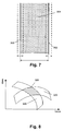
- the imaging imbalance of the phase shift mask 100 or the quality of the corresponding lithographic process is evaluated within the specific process window. Fig.
- the edges 302 of a printed line 304 and the line shift caused by the image imbalance can be taken into account for evaluating image imbalance.
- the feature size e.g. line width
- the position of the edges 302 of the feature 304, e.g. line are taken into account.
- the process windows 320 are determined for each edge 302 and the process window 322 used for evaluating is extracted as the overlapping region of these process windows 320.
- the process window 320 for an edge may be determined in any suitable way, such as e.g. based on obtaining a 10% difference between the design and the obtained structure. Extraction of the processing window 322 for evaluation is illustrated in Fig. 8, the dashed area indicating the process window for the lithographic processing of the specific feature 304 under study.
- the invention relates to a processing system wherein the designing or creating method embodiments according to the present invention are at least partly implemented, or in other words, to a processing system adapted for performing a method for designing or creating an alternating phase shift mask wherein the dose is taken into account for determining the mask parameters.
- An exemplary processing system 400 is shown in Fig. 9.
- Fig. 9 shows one configuration of processing system 400 that includes at least one programmable processor 403 coupled to a memory subsystem 405 that includes at least one form of memory, e.g., RAM, ROM, and so forth.
- a storage subsystem 407 may be included that has at least one disk drive and/or CD-ROM drive and/or DVD drive.
- a display system, a keyboard, and a pointing device may be included as part of a user interface subsystem 409 to provide for a user to manually input information. Ports for inputting and outputting data also may be included. More elements such as network connections, interfaces to various devices, and so forth, may be included, but are not illustrated in Fig. 9.
- the various elements of the processing system 400 may be coupled in various ways, including via a bus subsystem 413 shown in Fig. 9 for simplicity as a single bus, but will be understood to those in the art to include a system of at least one bus.
- the memory of the memory subsystem 405 may at some time hold part or all (in either case shown as 411) of a set of instructions that when executed on the processing system 400 implement the step(s) of the method embodiments described herein.
- a processing system 400 such as shown in Fig. 9 is prior art
- a system that includes the instructions to implement aspects of the present invention is not prior art, and therefore Fig. 9 is not labelled as
- processor 403 or processors may be a general purpose, or a special purpose processor, and may be for inclusion in a device, e.g., a chip that has other components that perform other functions.
- processors may be implemented in digital electronic circuitry, or in computer hardware, firmware, software, or in combinations of them.
- aspects of the invention can be implemented in a computer program product tangibly embodied in a carrier medium carrying machine-readable code for execution by a programmable processor. Method steps of aspects of the invention may be performed by a programmable processor executing instructions to perform functions of those aspects of the invention, e.g., by operating on input data and generating output data.
- the present invention includes a computer program product which provides the functionality of any of the methods according to the present invention when executed on a computing device.
- the present invention includes a data carrier such as for example a CD-ROM or a diskette which stores the computer product in a machine-readable form and which executes at least one of the methods of the invention when executed on a computing device.
- a data carrier such as for example a CD-ROM or a diskette which stores the computer product in a machine-readable form and which executes at least one of the methods of the invention when executed on a computing device.
- a data carrier such as for example a CD-ROM or a diskette which stores the computer product in a machine-readable form and which executes at least one of the methods of the invention when executed on a computing device.
- a data carrier such as for example a CD-ROM or a diskette which stores the computer product in a machine-readable form and which executes at least one of the methods of the invention when executed on a computing device.
- Fig. 11 illustrates a graph of the etch depth as a function of the pitch for different doses such that an optimally reduced image imbalance occurs.
- the latter also indicates that, for designing or making a mask, taking the illumination dose into account may result in different etch depths. Using other etch depths then results in increased image imbalance.
- Fig. 12a and Fig. 12b illustrate the maximum allowed line displacement slope in order to obtain an allowable process window for different pitches.
- a relation between the depth of focus (DOF) at 8% exposure latitude and the line displacement slope is given for a 130 nm pitch and a 220 nm pitch respectively.
- the allowed line displacement slope at 130 nm pitch is 0.007 ⁇ m/ ⁇ m
- the allowed line displacement slope at 220 nm is 0.015 ⁇ m/ ⁇ m
- the allowed line displacement slope at 350 nm is 0.017 ⁇ m/ ⁇ m.
- the latter may be used in combination with Fig. 10a to Fig. 10g to evaluate for which doses a specific etching depth can be used.
- lithographic processing can be obtained with a large process window for a wide range of pitches, i.e. including for the smallest pitches, allowing lithographic processing not suffering severely from image imbalance.
- the latter is obtained by taking into account the threshold, or taking into account the dose, in the image imbalance compensation optimisation.
Abstract
Description
- The present invention relates to methods and systems for lithographic processing of a device. More particularly, the present invention relates to lithographic alternating phase shift masks, methods of making them and methods of using lithographic alternating phase shift masks.
- Lithographic processing is one of the key features in the manufacturing of today's circuits and integrated components. The quality of the lithographic processing is strongly dependent on the lithographic system and the mask used. Different types of lithographic masks are known such as binary masks, like chrome on glass masks and phase shift masks, such as e.g. alternating phase shift masks and attenuated phase shift masks.
- The use of alternating phase shift masks (Alternating PSM) is a strong imaging technique combining high contrast and a low mask error enhancement factor (MEEF) with a large focus depth, especially for dense features. Alternating phase shift masks are masks wherein transmitting areas are used having a 180° phase difference with other transmitting areas of the mask. A feature on mask thereby is always surrounded by transmitting regions of different phase. The occurrence of the phase difference leads to destructive interference, resulting in a sharp dark image.
- A disadvantage of the use of alternating phase shift masks is the occurrence of image imbalance, which is intrinsically related to alternating phase shift mask imaging, leading to focus-dependent feature shifts. An appropriate compensation for the induced focus-dependent feature shifts, such as e.g. line displacements, is needed in order to fully exploit the advantages of alternating phase shift mask imaging.
- In general, two types of feature shift can be distinguished. Feature shift can originate from light scattering in the trenches of the alternating phase shift mask. An alternative source for image imbalance is the occurrence of a phase error, e.g. by a wrong effective phase shift of the light in the trenches. This might be caused by a mask fabrication error but also can be due to an intrinsic 3D effect due to the small feature sizes involved. Even a perfect mask, such as e.g. a simulated mask, can suffer from these intrinsic 3D effects, and thus from this type of image imbalance.
- Several image imbalance compensation strategies are known: Some examples of structural changes to the mask for compensating intensity imbalance are shown in Fig. 1a to Fig. 1c. Fig. 1 a illustrates a
mask 10 with compensation by undercut of the blocking region, indicated by the dashed region, adjacent a π-phase region, i.e. providing some undercut of the light-blocking layer, e.g. chrome layer. Fig. 1b shows amask 20 with compensation by double trenching whereby a shallow trench is provided at the 0 phase region at the left of the blocking region, indicated by the dashed region. Fig. 1c shows amask 30 with compensation by trench-space biasing for the π phase region at the right of the blocking region indicated by the dashed region. Providing undercut, using double trenching, using double patterning or applying side-wall chrome alternating aperture mask features may allow reduction of image imbalance caused by scattering. In order to reduce image imbalance caused by phase errors e.g. double exposure may be performed or additional measures can be taken when manufacturing the mask, such as e.g. an etch stop layer may be provided to avoid micro-loading. - Further optimisation for compensation, control and evaluation of intensity imbalance is useful, e.g. in view of the evolution towards high numerical aperture or hyper numerical aperture lithography systems and the associated shrinkage of features sizes and pitches, which puts stronger demands on the placement of the printed features e.g. in order to meet the overlay requirements.
- It is an object of the present invention to provide improved phase shift masks, methods of manufacturing such improved phase shift masks and methods for using such improved phase shift masks. It is an advantage of embodiments of the present invention to provide phase shift masks allowing reduction of image imbalance during lithographic processing of a device.
- The above objective is accomplished by a method and device according to embodiments of the present invention.
- The present invention relates to a method for making a phase shift mask in or on a substrate, said phase shift mask being suitable for lithographic processing of a device using a predetermined illumination dose. The method comprises etching said substrate according to mask parameters, wherein said mask parameters are selected taking into account said illumination dose. Selecting mask parameters may be selecting values for said mask parameters. Etching said substrate may comprise forming a trench in said substrate, wherein said mask parameters may comprise at least an etching depth for a trench. In other words, a value for said etching depth, corresponding with the trench depth, may be selected taking into account said illumination dose. Said mask parameters also may comprise a trench bias and a light blocking part bias, e.g. a Chrome width. In other words the light blocking part bias and/or the trench bias may be determined taking into account the illumination dose.
- The invention also relates to a method of designing a phase shift mask suitable for lithographic processing of a device using a predetermined illumination dose. The method comprises selecting a set of mask parameters taking into account said illumination dose. Said selecting a set of mask parameters may comprise selecting a plurality of sets of mask parameters suitable for using said phase shift mask substantially in focus, and selecting from said plurality of sets of mask parameters at least one set of mask parameters suitable for using said phase shift mask with said illumination dose in a predetermined out of focus range.
- In a method according to an embodiment of the present invention, said mask may comprise at least a trench and light blocking parts and said mask parameters may comprise at least a trench bias, a light blocking part bias and an etching depth of said trench, said mask being suitable for printing features on a device. Selecting a plurality of sets of mask parameters suitable for using said phase shift mask substantially in focus may comprise adjusting the light blocking part bias to correct a feature size and adjusting the trench bias to correct a feature position.
- Said trench bias and said light blocking part bias may be optimised for a predetermined range of doses, a predetermined range of etching depths and/or a predetermined range of pitches.
- Said mask may comprise at least a trench and said mask parameters may comprise at least an etching depth of said trench, whereby said selecting at least one set of mask parameters suitable for using said phase shift mask with said illumination dose in a predetermined out of focus range, may comprise selecting a set of mask parameters corresponding with a predetermined etching depth.
- Said selecting at least one set of mask parameters suitable for using said phase shift mask with said illumination dose in a predetermined out of focus range may comprise determining any of a focus-exposure matrix or an amount of feature displacement for a feature printable using said mask for said plurality of sets of mask parameters, and evaluating said focus exposure matrix or said amount of feature displacement for a feature printable using said mask.
- Said method may comprise evaluating a focus-exposure window for a feature printable using said mask, wherein said focus-exposure window is determined by a part of focus-exposure windows for at least two edges of said feature printable using said mask. With a common part of the focus-exposure windows for at least two edges of said feature printable using said mask there may be meant that the focus-exposure window used for evaluating is determined by the overlapping part of the focus-exposure windows for the edges of the feature printable using said mask.
- The invention also relates to a method for performing lithographic processing of a device, the method comprising using a phase shift mask and using an illumination dose, wherein one of said phase shift mask and said illumination dose are selected as a function of the other. For a predetermined illumination dose, said phase shift mask may be made according to any of the methods for making a phase shift mask as described above or said phase shift mask may be made according to any of the methods for designing as described above For a predetermined phase shift mask, an illumination dose may be selected as function of mask parameters of said phase shift mask. Said selection may be performed as a function of a depth of a trench in said phase shift mask.
- The present invention furthermore relates to a phase shift mask suitable for lithographic processing of a device using a predetermined illumination dose, the phase shift mask comprising a substrate with at least one means for generating a phase shift, a geometric size of said means for generating a phase shift being determined taking into account said illumination dose. Said geometrical size may be e.g. a thickness of a phase shift film or a depth of a trench in a transparent material. Said geometrical size may e.g. be a width and/or a depth of a trench or a width of a light blocking part.
- The invention also relates to a computer program product for designing a phase shift mask according to a method for designing as described above. It furthermore relates to a machine readable data storage device storing such a computer program product, or to the transmission of such a computer program product over a local or wide area telecommunications network.
- It is an advantage of embodiments of the present invention that lithographic processing with a reduced image imbalance is obtained for a wide range of pitches.
- It is also an advantage of embodiments of the present invention that setting up lithographic processing with a phase shift mask according to embodiments of the present invention requires less optimization.
- It is furthermore an advantage of embodiments of the present invention that lithographic processing can be performed resulting in line widths and line positions that are within the critical dimension and overlay specifications in a sufficiently large dose-focus window.
- Particular and preferred aspects of the invention are set out in the accompanying independent and dependent claims. Features from the dependent claims may be combined with features of the independent claims and with features of other dependent claims as appropriate and not merely as explicitly set out in the claims.
- The teachings of the present invention permit the design of improved alternating phase shift masks resulting in improved lithographic processing.
- The above and other characteristics, features and advantages of the present invention will become apparent from the following detailed description, taken in conjunction with the accompanying drawings, which illustrate, by way of example, the principles of the invention. This description is given for the sake of example only, without limiting the scope of the invention. The reference figures quoted below refer to the attached drawings.
-
- Fig. 1a to Fig. 1c show alternating phase shift masks comprising compensation features for image imbalance as known from prior art.
- Fig. 1d shows a graph of the line displacement as a function of a phase error generated by an alternating phase shift mask.
- Fig. 1e shows a graph of the line displacement as a function of the phase error caused by trench bias differences of an alternating phase shift mask.
- Fig. 2 shows an alternating phase shift mask with a trench depth taking into account the threshold of illumination, according to a first embodiment of the present invention.
- Fig. 3 shows a schematic overview of a method for designing an alternating phase shift mask according to embodiments of the present invention.
- Fig. 4 shows a schematic overview of a method for constructing an alternating phase shift mask according to embodiments of the present invention.
- Fig. 5a to Fig. 5h show different intermediate stages of an alternating phase shift mask during a method of construction of such a mask according to embodiments of the present invention.
- Fig. 6a to Fig. 6i show different intermediate stages of an alternating phase shift mask during an alternative method of construction of such a mask according to embodiments of the present invention.
- Fig. 7 illustrates the displacements for each of the edges of a printed feature, as is used to evaluate image imbalance in methods according to embodiments of the present invention.
- Fig. 8 illustrates the focus-dose process window as used for evaluation of the image imbalance, according to embodiments of the present invention.
- Fig. 9 shows a processing system adapted for performing at least part of any of the method embodiments according to the present invention.
- Fig. 10a to Fig. 10g show graphs of the line displacement slopes as a function of pitches for different doses of illumination used during lithographic processing with the corresponding alternating phase shift mask and for different etching depths used.
- Fig. 11 shows a graph of the optimal etch depth as a function of the pitch for different doses of illumination used during lithographic processing with the corresponding alternating phase shift mask.
- Fig. 12a to Fig. 12b shows a graph of the depth of focus as a function of the line displacement slope for different pitches.
- In the different figures, the same reference signs refer to the same or analogous elements.
- The present invention will be described with respect to particular embodiments and with reference to certain drawings but the invention is not limited thereto but only by the claims. The drawings described are only schematic and are non-limiting. In the drawings, the size of some of the elements may be exaggerated and not drawn on scale for illustrative purposes. The dimensions and the relative dimensions do not correspond to actual reductions to practice of the invention.
- Furthermore, the terms first, second, third and the like in the description and in the claims, are used for distinguishing between similar elements and not necessarily for describing a sequential or chronological order. It is to be understood that the terms so used are interchangeable under appropriate circumstances and that the embodiments of the invention described herein are capable of operation in other sequences than described or illustrated herein.
- It is to be noticed that the term "comprising", used in the claims, should not be interpreted as being restricted to the means listed thereafter; it does not exclude other elements or steps. It is thus to be interpreted as specifying the presence of the stated features, integers, steps or components as referred to, but does not preclude the presence or addition of one or more other features, integers, steps or components, or groups thereof. Thus, the scope of the expression "a device comprising means A and B" should not be limited to devices consisting only of components A and B. It means that with respect to the present invention, the only relevant components of the device are A and B.
- The invention will now be described by a detailed description of several embodiments of the invention. It is clear that other embodiments of the invention can be configured according to the knowledge of persons skilled in the art without departing from the true spirit or technical teaching of the invention, the invention being limited only by the terms of the appended claims.
- In a first embodiment, the present invention relates to an alternating phase shift mask, which can e.g. be used for lithographic processing of a device. The alternating phase shift mask of the present embodiment has mask parameters determined taking into account the threshold of illumination or the dose of illumination that will be used in lithographic processing for the alternating phase shift mask manufactured according to embodiments of the present invention. The mask typically will contain mask features such that it can be used for generation of a pattern on a device. An alternating phase shift mask typically comprises, in parts of the mask that are not blocking, means for generating a phase shift near the mask features such that, at such locations, destructive interference occurs and features can be imaged with a high contrast. The means for generating a phase shift may be any suitable type of means, such as e.g. a means for phase shifting comprising a phase shifting film or comprising a phase shifting substrate with regions having different optical thickness. In a preferred embodiment, the means for generating a phase shift may be a trench in a phase shifting substrate, which forms the basis of the mask. Alternating phase shift masks are known to generate image imbalance thus creating displacement of the printed features. Typically image imbalance generates line displacement, as shown in Fig. 1d and Fig. 1e for line displacement generated by phase errors in the phase shift mask and for line displacement caused by trench bias differences respectively. Fig. 1d shows line displacements as function of the focus behaviour whereby
curve 42 typically shows line displacement for a phase smaller than the optimum phase is present,curve 44 illustrates the line displacement when no phase error is made andcurve 46 illustrates the line displacement when a phase larger than the optimum phase is present. Fig. 1e shows line displacements as function of the focus behaviour wherebycurve 52 shows typically line displacement for a too small trench bias,curve 54 shows typically line displacement for a correct trench bias andcurve 56 shows typically line displacement for a too large trench bias. - Surprisingly it has been found that, for determining the parameters of the means for generating a phase shift, it is advantageous to take into account the dose of illumination that will be applied to the mask when used in lithographic processing. Taking into account this dose of illumination allows reduction of image imbalance created by the alternating phase shift mask. Depending on the type of means for generating an alternating phase shift, the parameters involved may be the depth of a trench provided in a phase shifting substrate, the width of the trench, the shape of the trench, the thickness of a phase shifting film, the width of the phase shifting film, etc. It is to be noted that the amount of illumination may be expressed using parameters such as the dose of illumination or the threshold of the aerial image. Both parameters are related to each other by

- By way of example, an alternating
phase shift mask 100 is shown in Fig. 2, with asubstrate 102, a patternedlight blocking layer 104, such as e.g. a chromium layer, a firstphase shift region 106 and a secondphase shift region 108. The firstphase shift region 106 is referred to as a 0 phase shift region, as it provides no other phase shift than the one provided by the full substrate thickness, whereas the secondphase shift region 108 is referred to as a π phase shift region, as it provides a phase shift π with respect to light passing to the full substrate thickness. Such a π phase shift region is created by introducing atrench 110, such that the optical path length in thesubstrate 102 at the location of thetrench 110 is substantially smaller. The etching depth detch used for forming thetrench 110 thus determines the phase shift that is provided. - The alternating
phase shift mask 100 according to the present embodiment may allow obtaining a reduction in image imbalance for a large process window and for a large number of pitches. - The means for generating a phase shift furthermore may comprise a double trench, undercut or any other features for providing compensation for image imbalance, as known by the person skilled in the art. Furthermore, the
mask 100 may comprise additional features that are typically used in lithographic processing; such as for example Optical Proximity Correction (OPC) features, as known by a person skilled in the art. - In a second embodiment, the present invention relates to a method for designing an alternating
phase shift mask 100, whereby the amount of illumination, e.g. expressed by the dose of illumination or the threshold for illumination, used for illumination of the alternatingphase shift mask 100 during its later use in lithographic processing is taken into account already during the design stage. More precisely, especially for reducing image imbalance in the through focus behaviour, taking into account the dose may lead to significant improvements. As the lithographic process is sensitive to variations in the focus depth one should not only determine the dimensions of the features printed on a substrate at the optimal focus but also at focus settings which deviate from this optimal focus setting. The sensitivity of the lithographic process will depend on the mask parameters of the mask as manufactured as these parameters may deviate from the determined optimal mask parameters, e.g. phase error, trench bias error. An example of a method for designing 150 according to the present embodiment may comprise following standard and/or optional steps, as shown by way of illustration in Fig. 3. - In a
first step 152, the initial mask settings are provided. The initial mask settings typically correspond with conventional mask settings used by a person skilled in the art for obtaining a mask allowing creation of a pattern on a device during lithographic processing. These conventional mask settings typically may comprise an initial etch depth detch, an initial dose and typical pitches in agreement with the pattern to be made on the device during lithographic processing using the mask. Further settings of the mask, such as an initial bias for the light blocking material, such as e.g. an initial Chromium bias, and an initial trench bias may be selected. - In a
second step 154, allowable mask parameters are determined for best focus behaviour, whereby the allowable mask parameters are determined for a wide range of doses, i.e. for a wide range of thresholds for illumination that will be used during lithographic processing of a device with themask 100. Determining allowable mask parameters may e.g. be performed using the following steps. A set of mask parameters may be selected, as shown instep 156. These parameters can be based on the initial mask parameters provided in thefirst step 152, whereby several parameters may be varied within predetermined ranges. In adecision step 158, it is checked whether the image imbalance at best focus is under control, i.e. whether the image imbalance is not too large. The amount of image imbalance that is allowed depends on the specific lithographic processing. The latter may e.g. comprise evaluating whether the printed feature is at the correct position and has the correct width/lateral dimensions. It may comprise evaluating the position of the edges of the features separately. If the image imbalance at best focus is sufficiently small, the set of parameters are evaluated as allowable, as shown instep 160. These parameters may e.g. be stored in a memory and/or these parameters may e.g. be outputted. If the image imbalance is not sufficiently controlled, the parameters may be adjusted, as shown instep 162, and new evaluation of the image imbalance may be made. Typical parameters that may be adjusted are the light blocking part bias, such as e.g. the chromium bias, in order to get the correct resist feature size, e.g. line width, and/or the trench bias to get the correct feature position, although the invention is not limited thereto. These parameters typically are evaluated for a setting of a dose in a predetermined range, an etching depth in a predetermined range and a pitch in a predetermined range. Such variation may be done systematically such that a whole parameter space is evaluated for predetermined ranges of each parameter. The evaluation preferably is done by simulating the obtained results for an alternating phase shift mask determined by the selected parameters and using the provided dose, although the latter in principle also could be determined through theoretical calculations or through experiments. A typical simulation engine that may be used is Prolith as available from KLA-Tencor, such as e.g. Protlith version 8.1 comprising the mask topography option. To determine the optimum mask parameters, rigorous simulation of the electromagnetic effects of light transmission through the mask topography may be used. - After selecting a number of allowable mask parameters for best focus behaviour, the through focus behaviour is determined for the allowable mask parameters, as shown in
step 164. The allowable mask parameters thereby typically may be allowable settings for the light blocking part bias and trench bias for a given dose, a given etching depth and a given pitch. Determining the through focus behaviour, i.e. the behaviour for focus settings differing from the best focus, may comprise calculating a mask error enhancement factor, a focus - exposure matrix for the features provided on the mask, positional information of the features provided on the mask and a line displacement slope for different pitches as a function of the dose. Typically, for an optimised trench bias and light blocking part bias, studying the line displacement slope as a function of the dose may allow evaluation of the through focus behaviour. Taking into account the obtained results, selection of the optimum etching depth taking into account the adequate dose is performed for the through focus behaviour, or selection of the optimum dose taking into account the adequate etching depth is performed for through focus behaviour, whereby the selection is made from the sets of allowable mask parameters. The latter typically results in optimum mask parameters for both best focus and through focus behaviour. Such parameters selected duringstep 166 may e.g. be used as input for a manufacturing method for making a phase shift mask. - It is an advantage of the present invention that the illumination dose is taken into account for matching the etch process to the optimum etch depth. In other words, either the optimum etch depth may be altered for a given dose or for a given etch depth an optimum dose may be selected. In one embodiment of the present invention the etch process may be selected taking into account a given dose. It is known from Philipsen et al. in proceedings of the PhotoMask Japan PMJ conference 2004, that different etches, and thus different etch depths, may lead to alternating phase shift masks having different properties. Taking into account the dose of illumination, an optimum selection of the etch for making an alternating phase shift mask may be selected.
- The evaluation processes may be performed in an automated way e.g. based on specific computer implemented algorithms, neural networks, etc. The method of designing may e.g. make use of software means such as electronic design automation tools. Starting from an initial design, a new design can be generated by manipulating the pattern info of this given design by means of software, e.g. varying the dimensions, deleting or adding features, etc.
- In the
exemplary method 150, first optimisation for image imbalance reduction is performed at best focus behaviour and subsequently optimisation is performed for image imbalance reduction at through focus behaviour. It is to be noted that these steps may be altered in timing, i.e. such that first optimisation for image imbalance reduction is performed at through focus behaviour and then optimisation for image imbalance reduction is performed at best focus behaviour. Furthermore optimisation of the mask parameters is performed as a function of the adequate dose. In an alternative embodiment, selection of an adequate dose may be performed for a given etch depth, e.g. if a given etch process is to be used. - In a third embodiment, the present invention relates to a method of making a
phase shift mask 100. In the present embodiment, the method for making thephase shift mask 100 is characterised by taking into account the threshold for illumination which will be used in the lithographic process for which the phase shift mask will be used, for determining the optimum mask parameters. In other words the dose or threshold that will be used for lithographic processing with thephase shift mask 100 under construction, is taken into account. Themethod 200 for creating a mask is illustrated by way of example in Fig. 4. Themethod 200 for creating a mask comprises thestep 202 of obtaining mask parameters for a phase shift mask according to any of the device embodiments as described above. The mask parameters of the phase shift mask thus are obtained taking into account the dose of the illumination in the lithographic processing for which the phase shift mask will be used. Thestep 202 of obtaining may comprise receiving the necessary mask information or determining, e.g. calculating, measuring and/or deriving, the necessary mask information. In a specific embodiment, the step of obtaining may comprise themethod 150 of designing aphase shift mask 100 as e.g. described in the second embodiment of the present invention. In asecond step 204, the mask will be generated, using the mask parameters as obtained instep 202. As the actual technique used for shifting the phase of light on a mask is not limiting in the embodiment of the present invention, a number of different manufacturing steps for the production of the phase shift mask may be introduced. Typical method steps for the creation of a phase shift mask may comprise deposition of layers, lithographic processing of layers, etching steps and/or any other suitable construction or treatment step. By way of example, illustration of the mask creation will be provided for a phase shift mask wherein the phase shift of the light stems from the light travelling different optical path lengths in a phase shifting substrate material. - Two different processes for illustrating lithographic processing steps for creating an exemplary phase shift mask are illustrated in Fig. 5a to Fig. 5h and in Fig. 6a to Fig. 6i by way of example.
- In a first example, the method of creating or constructing a
phase shift mask 100 according to obtained mask parameter information comprises the step of creating means for generating a phase shift and the step of providing a blocking layer on the substrate in agreement with a pattern to be formed on a device, when the mask is used during lithographic processing. Creating means for generating a phase shift may e.g. be creating trenches in a phase shifting substrate. According to the present invention, the etching depth detch of the trenches may be determined taking into account the dose or threshold of illumination that will be used on the lithographic system with thephase shift mask 100. The latter may be done by selecting e.g. a specific type of etch or by selecting specific timings for an etch. A first example is shown in Fig. 5a to Fig. 5h. First asubstrate 102, typically made of a transparent material such as for example quartz or CaF is coated with alight blocking layer 104, such as e.g. a chrome layer, and coated with a resistlayer 222. Subsequently, the resist 222 is illuminated according to a pattern, developed and removed, such that no resist is present where no light blocking material is to be present, as shown in Fig. 5b. In a following step, the light blocking material pattern is created by etching light blocking material away according to the resist pattern, as shown in Fig. 5c. Subsequently, the remaining resistmaterial 222 may be removed, as shown in Fig. 5d. In a further step a new resistlayer 224 is applied, as shown in Fig. 5e and resist is removed where a trench is to be formed, as shown in Fig. 5f. In a following step, atrench 110 is etched, as shown in Fig. 5g. The length of the etching process thereby is determined by the mask parameters provided, thus the etch depth takes into account the dose or threshold for illumination that will be used in the lithographic processing performed with thephase shift mask 100 constructed according to the present embodiment. After the remaining resist is removed, a phase shift mask as shown in Fig. 5h is obtained. - In a second example, creation of a means for generating a phase shift and provision of a light blocking pattern is obtained in a slightly different way. In a first step, a
substrate 102, typically made of transparent material, is provided with alight blocking layer 104, such as e.g. a chromium layer although the invention is not limited thereto, and a resistlayer 222, as shown in Fig. 6a. The resist 222 is then selectively removed at places where atrench 110 is to be formed, shown in Fig. 6b, and thelight blocking layer 104 is selectively removed, shown in Fig. 6c, whereafter atrench 110 is formed, as can be seen in Fig. 6d. The etching of thetrench 110 is performed such that for the obtained etch depth or trench depth the dose with which themask 100 will be illuminated during its use in lithographic processing is taken into account. In a following step the remaining resist 222 is removed, as shown in Fig. 6e. After formation of thetrench 110, thelight blocking layer 104, e.g. chromium layer is patterned using a resistlayer 224, as can be seen in Fig. 6f, by selectively removing the resistlayer 224, shown in Fig. 6g, subsequently selectively etching the non-coveredlight blocking layer 104, as shown in Fig. 6h, and by removing the resistlayer 224. The samephase shift mask 100 as in the previous example is obtained. - It is to be understood that the above examples are only provided by way of illustration and that these are not limiting for the present invention. The type of lithography process, e.g. type of resist, type of irradiation, etc. and the specific way of forming the means for generating a phase shifting means and for forming the patterned non-blocking layer is not limiting for the present invention. Different processes may be known by a person skilled in the art, but in the present invention, during formation of the trench, the etching depth will be determined taking into account the threshold or dose for illumination by which the
mask 100 will be irradiated during use in lithographic processing. - In a further embodiment, when the etch depth as a function of the pitch is known, e.g. from Philipsen et al. in proceedings of the PhotoMask Japan PMJ conference 2004, an adequate dose choice allows to compensate micro-loading errors during mask fabrication.
- In a fourth embodiment, the phase shift mask according to embodiments of the present invention is used in lithographic processing of a device. In other words, in the fourth embodiment, the present invention relates to a method of lithographic processing of a device using a
phase shift mask 100 according to embodiments of the present invention, whereby thephase shift mask 100 is constructed taking into account the threshold for illumination or dose of illumination used for lithographic processing with themask 100, or in other words, whereby the threshold for illumination or dose of illumination used for determining the optimumphase shift mask 100 is used during lithographic processing. The latter allows obtaining a high degree of reduction of image imbalance, resulting in improved lithographic processing. The lithographic processing thus obtained allows obtaining a good print quality for a large processing window, thus resulting in a high yield of devices made. Furthermore, the latter also allows obtaining a through-pitch solution to print e.g. 65 nm lines whereby the image imbalance is taken into account. Typically such lithographic processing comprises covering a device with a resist layer, illuminating said resist layer using the mask, thus providing an illumination pattern on the resist layer and developing said resist in order to obtain a patter in the resist. Either positive or negative resists may be used in combination with a corresponding mask pattern, as well known by a person skilled in the art. In an alternative embodiment, for a phase shift mask made using a specific etch depth, the present invention may relate to lithographic processing, whereby the dose of illumination to be used for illuminating the phase shift mask may be determined taking into account the etch depth used for the mask. In other words, the focus-exposure matrices of the edges of printed features are analysed in order to capture the line displacement due to image imbalance in the process window. It is an advantage that the position of the edges of the feature are evaluated separately, thus allowing an improved lithographic process compared to evaluation of the size of the whole feature. - In a fifth embodiment, the present invention relates to a
method 150 of designing aphase shift mask 100, amethod 200 for making aphase shift mask 100 or a method of lithographic processing using aphase shift mask 100, wherein the quality of thephase shift mask 100 is determined using a process window derived from the image imbalance for the edges of the mask features. The process window for evaluating imaging imbalance may be selected based on the position of theedges 302 of printedfeatures 304 or simulated printed features and is not solely based on the width of printed features 304. The imaging imbalance of thephase shift mask 100 or the quality of the corresponding lithographic process is evaluated within the specific process window. Fig. 7 illustrates how theedges 302 of a printedline 304 and the line shift caused by the image imbalance, can be taken into account for evaluating image imbalance. Whereas typically the feature size, e.g. line width, is taken into account for evaluating the focus-exposure window or processing window, in the present embodiment the position of theedges 302 of thefeature 304, e.g. line, are taken into account. In particular, theprocess windows 320 are determined for eachedge 302 and theprocess window 322 used for evaluating is extracted as the overlapping region of theseprocess windows 320. Theprocess window 320 for an edge may be determined in any suitable way, such as e.g. based on obtaining a 10% difference between the design and the obtained structure. Extraction of theprocessing window 322 for evaluation is illustrated in Fig. 8, the dashed area indicating the process window for the lithographic processing of thespecific feature 304 under study. - In a sixth embodiment, the invention relates to a processing system wherein the designing or creating method embodiments according to the present invention are at least partly implemented, or in other words, to a processing system adapted for performing a method for designing or creating an alternating phase shift mask wherein the dose is taken into account for determining the mask parameters. An
exemplary processing system 400 is shown in Fig. 9. Fig. 9 shows one configuration ofprocessing system 400 that includes at least oneprogrammable processor 403 coupled to a memory subsystem 405 that includes at least one form of memory, e.g., RAM, ROM, and so forth. Astorage subsystem 407 may be included that has at least one disk drive and/or CD-ROM drive and/or DVD drive. In some implementations, a display system, a keyboard, and a pointing device may be included as part of auser interface subsystem 409 to provide for a user to manually input information. Ports for inputting and outputting data also may be included. More elements such as network connections, interfaces to various devices, and so forth, may be included, but are not illustrated in Fig. 9. The various elements of theprocessing system 400 may be coupled in various ways, including via abus subsystem 413 shown in Fig. 9 for simplicity as a single bus, but will be understood to those in the art to include a system of at least one bus. The memory of the memory subsystem 405 may at some time hold part or all (in either case shown as 411) of a set of instructions that when executed on theprocessing system 400 implement the step(s) of the method embodiments described herein. Thus, while aprocessing system 400 such as shown in Fig. 9 is prior art, a system that includes the instructions to implement aspects of the present invention is not prior art, and therefore Fig. 9 is not labelled as - It is to be noted that the
processor 403 or processors may be a general purpose, or a special purpose processor, and may be for inclusion in a device, e.g., a chip that has other components that perform other functions. Thus, one or more aspects of the present invention can be implemented in digital electronic circuitry, or in computer hardware, firmware, software, or in combinations of them. Furthermore, aspects of the invention can be implemented in a computer program product tangibly embodied in a carrier medium carrying machine-readable code for execution by a programmable processor. Method steps of aspects of the invention may be performed by a programmable processor executing instructions to perform functions of those aspects of the invention, e.g., by operating on input data and generating output data. Accordingly, the present invention includes a computer program product which provides the functionality of any of the methods according to the present invention when executed on a computing device. Further, the present invention includes a data carrier such as for example a CD-ROM or a diskette which stores the computer product in a machine-readable form and which executes at least one of the methods of the invention when executed on a computing device. Nowadays, such software is often offered on the Internet or a company Intranet for download, hence the present invention includes transmitting the computer product according to the present invention over a local or wide area network. - Specific examples and advantages of embodiments of the present invention will be illustrated by exemplary experiments for the 65 nm half pitch node for ArF lithography with a numerical aperture of 0.85 nm, indicating the surprisingly significant influence of the dose on the image imbalance caused by a mask and the correlation with the mask parameters.
- In a first experiment, the line displacement in micrometer per micrometer defocus is studied for different dose and different pitches, using different etch depths, i.e. using different trench depths. These results are illustrated in Fig. 10a to Fig. 10g for an etch depth of 163.9 nm, 166.4 nm, 168.9 nm, 171.4 nm, 173.9 nm, 176.4 nm and 178.9 nm respectively. The short horizontal lines at each pitch thereby indicate the tolerance /process window/margin of the line displacement slope at that pitch. In the different drawings, it is indicated that dependent on the dose the etch depth may lead to allowable image imbalance or unallowable image imbalance. The latter can be seen from the fact that results are obtained falling without the tolerance/process window/margin of the line displacement slope for some pitches. The latter confirms that taking into account the dose for determination of the etch depth to be used or, vice versa, taking into account the etch depth used for determination of the dose may lead to significant advantages, thus supporting the embodiments of the present invention. Fig. 11 illustrates a graph of the etch depth as a function of the pitch for different doses such that an optimally reduced image imbalance occurs. The latter also indicates that, for designing or making a mask, taking the illumination dose into account may result in different etch depths. Using other etch depths then results in increased image imbalance.
- Fig. 12a and Fig. 12b illustrate the maximum allowed line displacement slope in order to obtain an allowable process window for different pitches. In other words, a relation between the depth of focus (DOF) at 8% exposure latitude and the line displacement slope is given for a 130 nm pitch and a 220 nm pitch respectively. Assuming that at least a depth of focus of 0.3 µm is required, the allowed line displacement slope at 130 nm pitch is 0.007 µm/µm, the allowed line displacement slope at 220 nm is 0.015 µm/µm and the allowed line displacement slope at 350 nm is 0.017 µm/µm. The latter may be used in combination with Fig. 10a to Fig. 10g to evaluate for which doses a specific etching depth can be used.
- It is an advantage of embodiments of the present invention that lithographic processing can be obtained with a large process window for a wide range of pitches, i.e. including for the smallest pitches, allowing lithographic processing not suffering severely from image imbalance. The latter is obtained by taking into account the threshold, or taking into account the dose, in the image imbalance compensation optimisation.
- It is an advantage of embodiments of the present invention that high quality lithographic processing is obtained for high numerical aperture or hyper numerical aperture applications.
- It is to be understood that although preferred embodiments, specific constructions and configurations, as well as materials, have been discussed herein for devices according to the present invention, various changes or modifications in form and detail may be made without departing from the scope and spirit of this invention.
Claims (15)
- A method (200) for making a phase shift mask (100) in/on a substrate (102), said phase shift mask (100) suitable for lithographic processing of a device using a predetermined illumination dose, the method comprising
etching said substrate (102) according to mask parameters,
wherein said mask parameters are selected taking into account said illumination dose. - A method (200) according to claim 1, etching said substrate (102) comprises forming a trench (110) in said substrate (102), wherein said mask parameters comprise at least an etching depth for said trench (110).
- A method of designing (150) a phase shift mask (100), suitable for lithographic processing of a device using a predetermined illumination dose, the method (150) comprising selecting a set of mask parameters taking into account said illumination dose.
- A method (150) according to claim 3, wherein said selecting a set of mask parameters comprises- selecting a plurality of sets of mask parameters suitable for using said phase shift mask (100) substantially in focus,- selecting from said plurality of sets of mask parameters at least one set of mask parameters suitable for using said phase shift mask (100) with said illumination dose in a predetermined out of focus range.
- A method (150) according to any of claims 3 to 4, said mask (100) comprising at least a trench (110) and light blocking parts (104), said mask parameters comprising at least a trench bias, a light blocking part bias and an etching depth of said trench, said mask being suitable for printing features on a device wherein selecting a plurality of sets of mask parameters suitable for using said phase shift mask (100) substantially in focus comprises adjusting the light blocking part bias to correct a feature size and adjusting the trench bias to correct a feature position.
- A method (150) according to any of claims 3 to 5, said mask (100) comprising at least a trench (110) and said mask parameters comprising at least an etching depth of said trench (110), said selecting at least one set of mask parameters suitable for using said phase shift mask (100) with said illumination dose in a predetermined out of focus range, comprising selecting a set of mask parameters corresponding with a predetermined etching depth.
- A method (150) according to any of claims 3 to 6, wherein said selecting at least one set of mask parameters suitable for using said phase shift mask with said illumination dose in a predetermined out of focus range comprises- determining any of a focus-exposure matrix or an amount of feature displacement for a feature printable using said mask for said plurality of sets of mask parameters and- evaluating said any of a focus exposure matrix or an amount of feature displacement for a feature printable using said mask.
- A method according to any of claims 3 to 7, wherein method comprises evaluating a focus-exposure window (322) for a feature printable using said mask, wherein said focus-exposure window (322) is determined by a common part of focus-exposure windows (320) for at least two edges of said feature printable using said mask (100).
- A method for performing lithographic processing of a device, the method comprising using a phase shift mask (100) and using an illumination dose,
wherein one of said phase shift mask (100) and said illumination dose are selected as a function of the other. - A method according to claim 9, whereby for a predetermined illumination dose, said phase shift mask (100) is made according to any of claims 1 to 2 or said phase shift mask (100) is designed according to any of claims 3 to 8.
- A method according to claim 9, whereby for a predetermined phase shift mask (100), an illumination dose is selected as function of mask parameters of said phase shift mask (100).
- A phase shift mask (100) suitable for lithographic processing of a device using a predetermined illumination dose,
the phase shift mask (100) comprising a substrate (102) with at least one means for generating a phase shift (110), a size of said means for generating a phase shift (110) being determined taking into account said illumination dose. - A computer program product for designing a phase shift mask according to any of claims 3 to 9.
- A machine readable data storage device storing the computer program product of claim 13.
- Transmission of the computer program product according to claim 13 over a local or wide area telecommunications network.
Priority Applications (5)
| Application Number | Priority Date | Filing Date | Title |
|---|---|---|---|
| AT05447222T ATE467149T1 (en) | 2005-10-03 | 2005-10-03 | ALTERNATE PHASE MASK |
| DE602005021106T DE602005021106D1 (en) | 2005-10-03 | 2005-10-03 | Alternating phase mask |
| EP05447222A EP1770439B1 (en) | 2005-10-03 | 2005-10-03 | Alternating phase shift mask |
| JP2006271857A JP5084217B2 (en) | 2005-10-03 | 2006-10-03 | Alternating phase shift mask |
| US11/543,302 US7761837B2 (en) | 2005-10-03 | 2006-10-03 | Method of making alternating phase shift masks |
Applications Claiming Priority (1)
| Application Number | Priority Date | Filing Date | Title |
|---|---|---|---|
| EP05447222A EP1770439B1 (en) | 2005-10-03 | 2005-10-03 | Alternating phase shift mask |
Publications (2)
| Publication Number | Publication Date |
|---|---|
| EP1770439A1 true EP1770439A1 (en) | 2007-04-04 |
| EP1770439B1 EP1770439B1 (en) | 2010-05-05 |
Family
ID=35482116
Family Applications (1)
| Application Number | Title | Priority Date | Filing Date |
|---|---|---|---|
| EP05447222A Not-in-force EP1770439B1 (en) | 2005-10-03 | 2005-10-03 | Alternating phase shift mask |
Country Status (5)
| Country | Link |
|---|---|
| US (1) | US7761837B2 (en) |
| EP (1) | EP1770439B1 (en) |
| JP (1) | JP5084217B2 (en) |
| AT (1) | ATE467149T1 (en) |
| DE (1) | DE602005021106D1 (en) |
Families Citing this family (7)
| Publication number | Priority date | Publication date | Assignee | Title |
|---|---|---|---|---|
| EP1804119A1 (en) * | 2005-12-27 | 2007-07-04 | Interuniversitair Microelektronica Centrum | Method for manufacturing attenuated phase- shift masks and devices obtained therefrom |
| DE102007031691A1 (en) | 2007-07-06 | 2009-01-08 | Carl Zeiss Smt Ag | Method for operating micro-lithographic projection lighting system, involves illuminating alternating phase shift mask with projection light, which has approximately coherent lighting angle distribution with coherence parameter |
| US10534257B2 (en) * | 2017-05-01 | 2020-01-14 | Lam Research Corporation | Layout pattern proximity correction through edge placement error prediction |
| US10572697B2 (en) | 2018-04-06 | 2020-02-25 | Lam Research Corporation | Method of etch model calibration using optical scatterometry |
| WO2019199697A1 (en) | 2018-04-10 | 2019-10-17 | Lam Research Corporation | Resist and etch modeling |
| KR20200130870A (en) | 2018-04-10 | 2020-11-20 | 램 리써치 코포레이션 | Optical instrumentation in machine learning to characterize features |
| US10846574B1 (en) * | 2019-07-12 | 2020-11-24 | Electronics For Imaging, Inc. | Variable smoothing in printing |
Family Cites Families (13)
| Publication number | Priority date | Publication date | Assignee | Title |
|---|---|---|---|---|
| JP3339174B2 (en) * | 1993-11-08 | 2002-10-28 | ソニー株式会社 | Photomask manufacturing method, exposure method, and semiconductor device manufacturing method |
| JP3388986B2 (en) * | 1996-03-08 | 2003-03-24 | 株式会社東芝 | Exposure mask and method of manufacturing the same |
| JP2002072442A (en) * | 2000-08-30 | 2002-03-12 | Sony Corp | Method for producing phase shift mask, resist pattern forming method and method for producing semiconductor device |
| JP2002118049A (en) * | 2000-10-06 | 2002-04-19 | Hitachi Ltd | Method for manufacturing semiconductor integrated circuit device |
| TWI252516B (en) * | 2002-03-12 | 2006-04-01 | Toshiba Corp | Determination method of process parameter and method for determining at least one of process parameter and design rule |
| JP4204858B2 (en) * | 2002-12-11 | 2009-01-07 | 大日本印刷株式会社 | Phase shift mask design method and design apparatus |
| JP2005084170A (en) * | 2003-09-05 | 2005-03-31 | Dainippon Printing Co Ltd | Method for designing and manufacturing phase shift mask, and apparatus for designing the phase shift mask |
| JP4539061B2 (en) * | 2003-09-08 | 2010-09-08 | 凸版印刷株式会社 | Phase shift mask manufacturing method, phase shift mask, and semiconductor device manufacturing method |
| SG111289A1 (en) * | 2003-11-05 | 2005-05-30 | Asml Masktools Bv | A method for performing transmission tuning of a mask pattern to improve process latitude |
| KR101056142B1 (en) * | 2004-01-29 | 2011-08-10 | 케이엘에이-텐코 코포레이션 | Computerized method for detecting defects in reticle design data |
| JP4351928B2 (en) * | 2004-02-23 | 2009-10-28 | 株式会社東芝 | Mask data correction method, photomask manufacturing method, and mask data correction program |
| US7642019B2 (en) * | 2005-04-15 | 2010-01-05 | Samsung Electronics Co., Ltd. | Methods for monitoring and adjusting focus variation in a photolithographic process using test features printed from photomask test pattern images; and machine readable program storage device having instructions therefore |
| US7536670B2 (en) * | 2005-05-31 | 2009-05-19 | Cadence Design Systems, Inc. | Method for verifying and choosing lithography model |
-
2005
- 2005-10-03 DE DE602005021106T patent/DE602005021106D1/en active Active
- 2005-10-03 EP EP05447222A patent/EP1770439B1/en not_active Not-in-force
- 2005-10-03 AT AT05447222T patent/ATE467149T1/en not_active IP Right Cessation
-
2006
- 2006-10-03 US US11/543,302 patent/US7761837B2/en not_active Expired - Fee Related
- 2006-10-03 JP JP2006271857A patent/JP5084217B2/en not_active Expired - Fee Related
Non-Patent Citations (6)
| Title |
|---|
| DRAPEAU ET AL.: "A practical alternating PSM modeling and OPC approach to deal with 3D mask effects for the 65nm node and beyond", PROCEEDINGS OF THE SPIE, vol. 5992, 3 October 2005 (2005-10-03), 25th Annual BACUS Symposium on Photomask Technology, pages 59921T-1 - 59921T-11, XP002361842 * |
| GRIESINGER U A ET AL: "Balancing of alternating phase shifting masks for practical application: modeling and experimental verification", PROCEEDINGS OF THE SPIE, vol. 4186, 13 September 2000 (2000-09-13), 20th Annual BACUS Symposium on Photomask Technology, pages 372 - 383, XP002361839, ISSN: 0277-786X * |
| LA COUR ET AL.: "Prediction of design sensitivity to altPSM lithography across process window", PROCEEDINGS OF THE SPIE, vol. 5567, 14 September 2004 (2004-09-14), 24th Annual BACUS Symposium on Photomask Technology, pages 604 - 613, XP002361838 * |
| NAKAZAWA K ET AL: "Fabrication of 0.1 [mu]m patterns using an alternating phase shift mask in ArF excimer laser lithography", JAPANESE JOURNAL OF APPLIED PHYSICS, PART 1 (REGULAR PAPERS, SHORT NOTES & REVIEW PAPERS) PUBLICATION OFFICE, JAPANESE JOURNAL APPL. PHYS JAPAN, vol. 36, no. 12B, December 1997 (1997-12-01), pages 7488 - 7493, XP002361840, ISSN: 0021-4922 * |
| V. PHILIPSEN; R. JONCKHEERE: "printability of topography in alternating phase-shift masks", PROCEEDINGS OF PHOTOMASK JAPAN 2004, 24TH ANNUAL BACUS SYMPOSIUM ON PHOTOMASK TECHNOLOGY, PROCEEDINGS SPIE, vol. 5567, pages 587 - 595 |
| VAN LOOK ET AL.: "Image imbalance compensation in alternating phase-shift masks towards the 45nm node through-pitch imaging", PROCEEDINGS OF THE SPIE, vol. 5992, 3 October 2005 (2005-10-03), 25th Annual BACUS Symposium on Photomask Technology, pages 59921S-1 - 59921S-12, XP002361841 * |
Also Published As
| Publication number | Publication date |
|---|---|
| JP2007102230A (en) | 2007-04-19 |
| ATE467149T1 (en) | 2010-05-15 |
| US20070087273A1 (en) | 2007-04-19 |
| JP5084217B2 (en) | 2012-11-28 |
| DE602005021106D1 (en) | 2010-06-17 |
| US7761837B2 (en) | 2010-07-20 |
| EP1770439B1 (en) | 2010-05-05 |
Similar Documents
| Publication | Publication Date | Title |
|---|---|---|
| US6830854B2 (en) | System and method for correcting 3D effects in an alternating phase-shifting mask | |
| US6635393B2 (en) | Blank for alternating PSM photomask with charge dissipation layer | |
| KR100714480B1 (en) | systems and methods for detecting focus variation in photolithograph process using test features printed from photomask test pattern images | |
| US7761837B2 (en) | Method of making alternating phase shift masks | |
| JP4074816B2 (en) | Method and apparatus for prioritizing the application of resolution enhancement techniques | |
| US6785879B2 (en) | Model-based data conversion | |
| KR100763222B1 (en) | Photomask structures providing improved photolithographic process windows and methods of manufacturing the same | |
| US6794096B2 (en) | Phase shifting mask topography effect correction based on near-field image properties | |
| JP2007535694A (en) | Embedded attenuation phase shift mask with adjustable transmittance | |
| US20070111112A1 (en) | Systems and methods for fabricating photo masks | |
| TWI388922B (en) | Pattern forming method and phase shift mask manufacturing method | |
| US6993455B2 (en) | Method for determining the construction of a mask for the micropatterning of semiconductor substrates by means of photolithography | |
| WO2005103820A1 (en) | Levenson type phase shift mask and production method therefor | |
| US7930654B2 (en) | System and method of correcting errors in SEM-measurements | |
| US7945869B2 (en) | Mask and method for patterning a semiconductor wafer | |
| US6395432B1 (en) | Methods of determining processing alignment in the forming of phase shift regions | |
| JP5313429B2 (en) | Optical lithography method | |
| JP2003177504A (en) | Data correcting method for phase shift mask | |
| US7251806B2 (en) | Model-based two-dimensional interpretation filtering | |
| US6933084B2 (en) | Alternating aperture phase shift photomask having light absorption layer | |
| KR20070068910A (en) | Method of correcting critical dimesion of a phase shift mask | |
| JP2007233138A (en) | Mask, method for manufacturing mask, and method for manufacturing semiconductor device using the mask | |
| US6720114B1 (en) | Method of forming an alternating phase shift circuitry fabrication mask, method of forming a circuitry fabrication mask having a subtractive alternating phase shift region, and alternating phase shift mask | |
| JP4314899B2 (en) | Method for manufacturing phase shift mask | |
| JP2002357889A (en) | Apparatus for manufacturing phase shifting mask, method therefor and pattern forming method using phase shifting mask |
Legal Events
| Date | Code | Title | Description |
|---|---|---|---|
| PUAI | Public reference made under article 153(3) epc to a published international application that has entered the european phase |
Free format text: ORIGINAL CODE: 0009012 |
|
| AK | Designated contracting states |
Kind code of ref document: A1 Designated state(s): AT BE BG CH CY CZ DE DK EE ES FI FR GB GR HU IE IS IT LI LT LU LV MC NL PL PT RO SE SI SK TR |
|
| AX | Request for extension of the european patent |
Extension state: AL BA HR MK YU |
|
| 17P | Request for examination filed |
Effective date: 20070912 |
|
| AKX | Designation fees paid |
Designated state(s): AT BE BG CH CY CZ DE DK EE ES FI FR GB GR HU IE IS IT LI LT LU LV MC NL PL PT RO SE SI SK TR |
|
| 17Q | First examination report despatched |
Effective date: 20080407 |
|
| RAP1 | Party data changed (applicant data changed or rights of an application transferred) |
Owner name: IMEC |
|
| GRAP | Despatch of communication of intention to grant a patent |
Free format text: ORIGINAL CODE: EPIDOSNIGR1 |
|
| GRAS | Grant fee paid |
Free format text: ORIGINAL CODE: EPIDOSNIGR3 |
|
| GRAA | (expected) grant |
Free format text: ORIGINAL CODE: 0009210 |
|
| STAA | Information on the status of an ep patent application or granted ep patent |
Free format text: STATUS: THE PATENT HAS BEEN GRANTED |
|
| AK | Designated contracting states |
Kind code of ref document: B1 Designated state(s): AT BE BG CH CY CZ DE DK EE ES FI FR GB GR HU IE IS IT LI LT LU LV MC NL PL PT RO SE SI SK TR |
|
| REG | Reference to a national code |
Ref country code: GB Ref legal event code: FG4D |
|
| REG | Reference to a national code |
Ref country code: CH Ref legal event code: EP |
|
| REG | Reference to a national code |
Ref country code: IE Ref legal event code: FG4D |
|
| REF | Corresponds to: |
Ref document number: 602005021106 Country of ref document: DE Date of ref document: 20100617 Kind code of ref document: P |
|
| REG | Reference to a national code |
Ref country code: NL Ref legal event code: VDEP Effective date: 20100505 |
|
| LTIE | Lt: invalidation of european patent or patent extension |
Effective date: 20100505 |
|
| PG25 | Lapsed in a contracting state [announced via postgrant information from national office to epo] |
Ref country code: LT Free format text: LAPSE BECAUSE OF FAILURE TO SUBMIT A TRANSLATION OF THE DESCRIPTION OR TO PAY THE FEE WITHIN THE PRESCRIBED TIME-LIMIT Effective date: 20100505 Ref country code: NL Free format text: LAPSE BECAUSE OF FAILURE TO SUBMIT A TRANSLATION OF THE DESCRIPTION OR TO PAY THE FEE WITHIN THE PRESCRIBED TIME-LIMIT Effective date: 20100505 Ref country code: ES Free format text: LAPSE BECAUSE OF FAILURE TO SUBMIT A TRANSLATION OF THE DESCRIPTION OR TO PAY THE FEE WITHIN THE PRESCRIBED TIME-LIMIT Effective date: 20100816 Ref country code: SE Free format text: LAPSE BECAUSE OF FAILURE TO SUBMIT A TRANSLATION OF THE DESCRIPTION OR TO PAY THE FEE WITHIN THE PRESCRIBED TIME-LIMIT Effective date: 20100505 |
|
| PG25 | Lapsed in a contracting state [announced via postgrant information from national office to epo] |
Ref country code: IS Free format text: LAPSE BECAUSE OF FAILURE TO SUBMIT A TRANSLATION OF THE DESCRIPTION OR TO PAY THE FEE WITHIN THE PRESCRIBED TIME-LIMIT Effective date: 20100905 Ref country code: FI Free format text: LAPSE BECAUSE OF FAILURE TO SUBMIT A TRANSLATION OF THE DESCRIPTION OR TO PAY THE FEE WITHIN THE PRESCRIBED TIME-LIMIT Effective date: 20100505 Ref country code: AT Free format text: LAPSE BECAUSE OF FAILURE TO SUBMIT A TRANSLATION OF THE DESCRIPTION OR TO PAY THE FEE WITHIN THE PRESCRIBED TIME-LIMIT Effective date: 20100505 Ref country code: SI Free format text: LAPSE BECAUSE OF FAILURE TO SUBMIT A TRANSLATION OF THE DESCRIPTION OR TO PAY THE FEE WITHIN THE PRESCRIBED TIME-LIMIT Effective date: 20100505 Ref country code: LV Free format text: LAPSE BECAUSE OF FAILURE TO SUBMIT A TRANSLATION OF THE DESCRIPTION OR TO PAY THE FEE WITHIN THE PRESCRIBED TIME-LIMIT Effective date: 20100505 |
|
| PG25 | Lapsed in a contracting state [announced via postgrant information from national office to epo] |
Ref country code: PL Free format text: LAPSE BECAUSE OF FAILURE TO SUBMIT A TRANSLATION OF THE DESCRIPTION OR TO PAY THE FEE WITHIN THE PRESCRIBED TIME-LIMIT Effective date: 20100505 Ref country code: GR Free format text: LAPSE BECAUSE OF FAILURE TO SUBMIT A TRANSLATION OF THE DESCRIPTION OR TO PAY THE FEE WITHIN THE PRESCRIBED TIME-LIMIT Effective date: 20100806 Ref country code: CY Free format text: LAPSE BECAUSE OF FAILURE TO SUBMIT A TRANSLATION OF THE DESCRIPTION OR TO PAY THE FEE WITHIN THE PRESCRIBED TIME-LIMIT Effective date: 20100505 |
|
| PG25 | Lapsed in a contracting state [announced via postgrant information from national office to epo] |
Ref country code: DK Free format text: LAPSE BECAUSE OF FAILURE TO SUBMIT A TRANSLATION OF THE DESCRIPTION OR TO PAY THE FEE WITHIN THE PRESCRIBED TIME-LIMIT Effective date: 20100505 Ref country code: PT Free format text: LAPSE BECAUSE OF FAILURE TO SUBMIT A TRANSLATION OF THE DESCRIPTION OR TO PAY THE FEE WITHIN THE PRESCRIBED TIME-LIMIT Effective date: 20100906 Ref country code: EE Free format text: LAPSE BECAUSE OF FAILURE TO SUBMIT A TRANSLATION OF THE DESCRIPTION OR TO PAY THE FEE WITHIN THE PRESCRIBED TIME-LIMIT Effective date: 20100505 |
|
| PG25 | Lapsed in a contracting state [announced via postgrant information from national office to epo] |
Ref country code: BE Free format text: LAPSE BECAUSE OF FAILURE TO SUBMIT A TRANSLATION OF THE DESCRIPTION OR TO PAY THE FEE WITHIN THE PRESCRIBED TIME-LIMIT Effective date: 20100505 Ref country code: CZ Free format text: LAPSE BECAUSE OF FAILURE TO SUBMIT A TRANSLATION OF THE DESCRIPTION OR TO PAY THE FEE WITHIN THE PRESCRIBED TIME-LIMIT Effective date: 20100505 Ref country code: RO Free format text: LAPSE BECAUSE OF FAILURE TO SUBMIT A TRANSLATION OF THE DESCRIPTION OR TO PAY THE FEE WITHIN THE PRESCRIBED TIME-LIMIT Effective date: 20100505 Ref country code: SK Free format text: LAPSE BECAUSE OF FAILURE TO SUBMIT A TRANSLATION OF THE DESCRIPTION OR TO PAY THE FEE WITHIN THE PRESCRIBED TIME-LIMIT Effective date: 20100505 |
|
| PLBE | No opposition filed within time limit |
Free format text: ORIGINAL CODE: 0009261 |
|
| STAA | Information on the status of an ep patent application or granted ep patent |
Free format text: STATUS: NO OPPOSITION FILED WITHIN TIME LIMIT |
|
| PG25 | Lapsed in a contracting state [announced via postgrant information from national office to epo] |
Ref country code: IT Free format text: LAPSE BECAUSE OF FAILURE TO SUBMIT A TRANSLATION OF THE DESCRIPTION OR TO PAY THE FEE WITHIN THE PRESCRIBED TIME-LIMIT Effective date: 20100505 |
|
| 26N | No opposition filed |
Effective date: 20110208 |
|
| REG | Reference to a national code |
Ref country code: DE Ref legal event code: R097 Ref document number: 602005021106 Country of ref document: DE Effective date: 20110207 |
|
| PG25 | Lapsed in a contracting state [announced via postgrant information from national office to epo] |
Ref country code: MC Free format text: LAPSE BECAUSE OF NON-PAYMENT OF DUE FEES Effective date: 20101031 |
|
| REG | Reference to a national code |
Ref country code: CH Ref legal event code: PL |
|
| PG25 | Lapsed in a contracting state [announced via postgrant information from national office to epo] |
Ref country code: LI Free format text: LAPSE BECAUSE OF NON-PAYMENT OF DUE FEES Effective date: 20101031 Ref country code: CH Free format text: LAPSE BECAUSE OF NON-PAYMENT OF DUE FEES Effective date: 20101031 |
|
| PG25 | Lapsed in a contracting state [announced via postgrant information from national office to epo] |
Ref country code: IE Free format text: LAPSE BECAUSE OF NON-PAYMENT OF DUE FEES Effective date: 20101003 |
|
| PG25 | Lapsed in a contracting state [announced via postgrant information from national office to epo] |
Ref country code: LU Free format text: LAPSE BECAUSE OF NON-PAYMENT OF DUE FEES Effective date: 20101003 Ref country code: BG Free format text: LAPSE BECAUSE OF FAILURE TO SUBMIT A TRANSLATION OF THE DESCRIPTION OR TO PAY THE FEE WITHIN THE PRESCRIBED TIME-LIMIT Effective date: 20100505 Ref country code: HU Free format text: LAPSE BECAUSE OF FAILURE TO SUBMIT A TRANSLATION OF THE DESCRIPTION OR TO PAY THE FEE WITHIN THE PRESCRIBED TIME-LIMIT Effective date: 20101106 |
|
| PG25 | Lapsed in a contracting state [announced via postgrant information from national office to epo] |
Ref country code: TR Free format text: LAPSE BECAUSE OF FAILURE TO SUBMIT A TRANSLATION OF THE DESCRIPTION OR TO PAY THE FEE WITHIN THE PRESCRIBED TIME-LIMIT Effective date: 20100505 |
|
| PG25 | Lapsed in a contracting state [announced via postgrant information from national office to epo] |
Ref country code: BG Free format text: LAPSE BECAUSE OF FAILURE TO SUBMIT A TRANSLATION OF THE DESCRIPTION OR TO PAY THE FEE WITHIN THE PRESCRIBED TIME-LIMIT Effective date: 20100805 |
|
| REG | Reference to a national code |
Ref country code: FR Ref legal event code: PLFP Year of fee payment: 12 |
|
| REG | Reference to a national code |
Ref country code: FR Ref legal event code: PLFP Year of fee payment: 13 |
|
| REG | Reference to a national code |
Ref country code: FR Ref legal event code: PLFP Year of fee payment: 14 |
|
| PGFP | Annual fee paid to national office [announced via postgrant information from national office to epo] |
Ref country code: FR Payment date: 20190919 Year of fee payment: 15 |
|
| PGFP | Annual fee paid to national office [announced via postgrant information from national office to epo] |
Ref country code: GB Payment date: 20190923 Year of fee payment: 15 |
|
| PGFP | Annual fee paid to national office [announced via postgrant information from national office to epo] |
Ref country code: DE Payment date: 20190918 Year of fee payment: 15 |
|
| REG | Reference to a national code |
Ref country code: DE Ref legal event code: R119 Ref document number: 602005021106 Country of ref document: DE |
|
| GBPC | Gb: european patent ceased through non-payment of renewal fee |
Effective date: 20201003 |
|
| PG25 | Lapsed in a contracting state [announced via postgrant information from national office to epo] |
Ref country code: FR Free format text: LAPSE BECAUSE OF NON-PAYMENT OF DUE FEES Effective date: 20201031 Ref country code: DE Free format text: LAPSE BECAUSE OF NON-PAYMENT OF DUE FEES Effective date: 20210501 |
|
| PG25 | Lapsed in a contracting state [announced via postgrant information from national office to epo] |
Ref country code: GB Free format text: LAPSE BECAUSE OF NON-PAYMENT OF DUE FEES Effective date: 20201003 |