EP1764830A2 - A method to create narrow trenches in dielectric materials - Google Patents
A method to create narrow trenches in dielectric materials Download PDFInfo
- Publication number
- EP1764830A2 EP1764830A2 EP05447238A EP05447238A EP1764830A2 EP 1764830 A2 EP1764830 A2 EP 1764830A2 EP 05447238 A EP05447238 A EP 05447238A EP 05447238 A EP05447238 A EP 05447238A EP 1764830 A2 EP1764830 A2 EP 1764830A2
- Authority
- EP
- European Patent Office
- Prior art keywords
- trenches
- making
- dielectric layer
- dielectric
- temporary structure
- Prior art date
- Legal status (The legal status is an assumption and is not a legal conclusion. Google has not performed a legal analysis and makes no representation as to the accuracy of the status listed.)
- Granted
Links
Images






Classifications
-
- H—ELECTRICITY
- H10—SEMICONDUCTOR DEVICES; ELECTRIC SOLID-STATE DEVICES NOT OTHERWISE PROVIDED FOR
- H10P—GENERIC PROCESSES OR APPARATUS FOR THE MANUFACTURE OR TREATMENT OF DEVICES COVERED BY CLASS H10
- H10P50/00—Etching of wafers, substrates or parts of devices
- H10P50/20—Dry etching; Plasma etching; Reactive-ion etching
- H10P50/28—Dry etching; Plasma etching; Reactive-ion etching of insulating materials
- H10P50/282—Dry etching; Plasma etching; Reactive-ion etching of insulating materials of inorganic materials
- H10P50/283—Dry etching; Plasma etching; Reactive-ion etching of insulating materials of inorganic materials by chemical means
-
- B—PERFORMING OPERATIONS; TRANSPORTING
- B81—MICROSTRUCTURAL TECHNOLOGY
- B81C—PROCESSES OR APPARATUS SPECIALLY ADAPTED FOR THE MANUFACTURE OR TREATMENT OF MICROSTRUCTURAL DEVICES OR SYSTEMS
- B81C1/00—Manufacture or treatment of devices or systems in or on a substrate
- B81C1/00436—Shaping materials, i.e. techniques for structuring the substrate or the layers on the substrate
- B81C1/00555—Achieving a desired geometry, i.e. controlling etch rates, anisotropy or selectivity
- B81C1/00595—Control etch selectivity
-
- H—ELECTRICITY
- H10—SEMICONDUCTOR DEVICES; ELECTRIC SOLID-STATE DEVICES NOT OTHERWISE PROVIDED FOR
- H10W—GENERIC PACKAGES, INTERCONNECTIONS, CONNECTORS OR OTHER CONSTRUCTIONAL DETAILS OF DEVICES COVERED BY CLASS H10
- H10W10/00—Isolation regions in semiconductor bodies between components of integrated devices
- H10W10/01—Manufacture or treatment
- H10W10/011—Manufacture or treatment of isolation regions comprising dielectric materials
- H10W10/014—Manufacture or treatment of isolation regions comprising dielectric materials using trench refilling with dielectric materials, e.g. shallow trench isolations
-
- H—ELECTRICITY
- H10—SEMICONDUCTOR DEVICES; ELECTRIC SOLID-STATE DEVICES NOT OTHERWISE PROVIDED FOR
- H10W—GENERIC PACKAGES, INTERCONNECTIONS, CONNECTORS OR OTHER CONSTRUCTIONAL DETAILS OF DEVICES COVERED BY CLASS H10
- H10W10/00—Isolation regions in semiconductor bodies between components of integrated devices
- H10W10/10—Isolation regions comprising dielectric materials
- H10W10/17—Isolation regions comprising dielectric materials formed using trench refilling with dielectric materials, e.g. shallow trench isolations
-
- H—ELECTRICITY
- H10—SEMICONDUCTOR DEVICES; ELECTRIC SOLID-STATE DEVICES NOT OTHERWISE PROVIDED FOR
- H10W—GENERIC PACKAGES, INTERCONNECTIONS, CONNECTORS OR OTHER CONSTRUCTIONAL DETAILS OF DEVICES COVERED BY CLASS H10
- H10W20/00—Interconnections in chips, wafers or substrates
- H10W20/01—Manufacture or treatment
- H10W20/071—Manufacture or treatment of dielectric parts thereof
- H10W20/081—Manufacture or treatment of dielectric parts thereof by forming openings in the dielectric parts
- H10W20/089—Manufacture or treatment of dielectric parts thereof by forming openings in the dielectric parts using processes for implementing desired shapes or dispositions of the openings, e.g. double patterning
-
- B—PERFORMING OPERATIONS; TRANSPORTING
- B81—MICROSTRUCTURAL TECHNOLOGY
- B81C—PROCESSES OR APPARATUS SPECIALLY ADAPTED FOR THE MANUFACTURE OR TREATMENT OF MICROSTRUCTURAL DEVICES OR SYSTEMS
- B81C2201/00—Manufacture or treatment of microstructural devices or systems
- B81C2201/01—Manufacture or treatment of microstructural devices or systems in or on a substrate
- B81C2201/0101—Shaping material; Structuring the bulk substrate or layers on the substrate; Film patterning
- B81C2201/0128—Processes for removing material
- B81C2201/013—Etching
- B81C2201/0132—Dry etching, i.e. plasma etching, barrel etching, reactive ion etching [RIE], sputter etching or ion milling
-
- B—PERFORMING OPERATIONS; TRANSPORTING
- B81—MICROSTRUCTURAL TECHNOLOGY
- B81C—PROCESSES OR APPARATUS SPECIALLY ADAPTED FOR THE MANUFACTURE OR TREATMENT OF MICROSTRUCTURAL DEVICES OR SYSTEMS
- B81C2201/00—Manufacture or treatment of microstructural devices or systems
- B81C2201/01—Manufacture or treatment of microstructural devices or systems in or on a substrate
- B81C2201/0101—Shaping material; Structuring the bulk substrate or layers on the substrate; Film patterning
- B81C2201/0128—Processes for removing material
- B81C2201/013—Etching
- B81C2201/0133—Wet etching
-
- H—ELECTRICITY
- H10—SEMICONDUCTOR DEVICES; ELECTRIC SOLID-STATE DEVICES NOT OTHERWISE PROVIDED FOR
- H10P—GENERIC PROCESSES OR APPARATUS FOR THE MANUFACTURE OR TREATMENT OF DEVICES COVERED BY CLASS H10
- H10P14/00—Formation of materials, e.g. in the shape of layers or pillars
- H10P14/60—Formation of materials, e.g. in the shape of layers or pillars of insulating materials
- H10P14/63—Formation of materials, e.g. in the shape of layers or pillars of insulating materials characterised by the formation processes
- H10P14/6326—Deposition processes
- H10P14/6328—Deposition from the gas or vapour phase
- H10P14/6334—Deposition from the gas or vapour phase using decomposition or reaction of gaseous or vapour phase compounds, i.e. chemical vapour deposition
-
- H—ELECTRICITY
- H10—SEMICONDUCTOR DEVICES; ELECTRIC SOLID-STATE DEVICES NOT OTHERWISE PROVIDED FOR
- H10P—GENERIC PROCESSES OR APPARATUS FOR THE MANUFACTURE OR TREATMENT OF DEVICES COVERED BY CLASS H10
- H10P14/00—Formation of materials, e.g. in the shape of layers or pillars
- H10P14/60—Formation of materials, e.g. in the shape of layers or pillars of insulating materials
- H10P14/63—Formation of materials, e.g. in the shape of layers or pillars of insulating materials characterised by the formation processes
- H10P14/6326—Deposition processes
- H10P14/6328—Deposition from the gas or vapour phase
- H10P14/6334—Deposition from the gas or vapour phase using decomposition or reaction of gaseous or vapour phase compounds, i.e. chemical vapour deposition
- H10P14/6336—Deposition from the gas or vapour phase using decomposition or reaction of gaseous or vapour phase compounds, i.e. chemical vapour deposition in the presence of a plasma [PECVD]
-
- H—ELECTRICITY
- H10—SEMICONDUCTOR DEVICES; ELECTRIC SOLID-STATE DEVICES NOT OTHERWISE PROVIDED FOR
- H10P—GENERIC PROCESSES OR APPARATUS FOR THE MANUFACTURE OR TREATMENT OF DEVICES COVERED BY CLASS H10
- H10P14/00—Formation of materials, e.g. in the shape of layers or pillars
- H10P14/60—Formation of materials, e.g. in the shape of layers or pillars of insulating materials
- H10P14/63—Formation of materials, e.g. in the shape of layers or pillars of insulating materials characterised by the formation processes
- H10P14/6326—Deposition processes
- H10P14/6342—Liquid deposition, e.g. spin-coating, sol-gel techniques or spray coating
-
- H—ELECTRICITY
- H10—SEMICONDUCTOR DEVICES; ELECTRIC SOLID-STATE DEVICES NOT OTHERWISE PROVIDED FOR
- H10P—GENERIC PROCESSES OR APPARATUS FOR THE MANUFACTURE OR TREATMENT OF DEVICES COVERED BY CLASS H10
- H10P14/00—Formation of materials, e.g. in the shape of layers or pillars
- H10P14/60—Formation of materials, e.g. in the shape of layers or pillars of insulating materials
- H10P14/69—Inorganic materials
- H10P14/692—Inorganic materials composed of oxides, glassy oxides or oxide-based glasses
- H10P14/6921—Inorganic materials composed of oxides, glassy oxides or oxide-based glasses containing silicon
- H10P14/6922—Inorganic materials composed of oxides, glassy oxides or oxide-based glasses containing silicon the material containing Si, O and at least one of H, N, C, F or other non-metal elements, e.g. SiOC, SiOC:H or SiONC
Definitions
- the present invention is related to the field of semiconductor processing.
- More specifically it is related to the production of micro and nano-electromechanical systems and to the production of low dielectric isolation for interconnects. It contributes to the exploration of the field of narrow trenches in semiconductor devices.
- Interconnects have been, are, and will continue to be a limiting factor for the performance and cost of integrated circuits. As technology scales down further, the problems associated with interconnects become ever more pressing. The introduction of low-resistive copper as an alternative interconnect material for aluminum presents researchers with some new challenges, since copper cannot be implemented in the same manner as aluminum alloys.
- trenches are getting proportionally deeper as they get narrower. These deep trenches etched into the dielectric must be filled completely, without voids or defects. With current technology, the deeper the trench, the more likely there will be defects.
- Double-Damascene methods are currently used to etch the trenches, fill them electrolytically, then mechanically polish away the excess metal using a chemically active slurry. Etching and filling narrow structures with high aspect ratios will be especially difficult for dual-Damascene architectures.
- the challenge is to address narrower trenches, the goal is to get down to a width of these trenches of about 20 to 30 nm, with an aspect ratio of 10 to 1 (ratio length to width).
- barrier deposition techniques such as ALD and CVD are not straight forward in these small trenches (having a width of 20-30 nm and aspect ratio of 10 to 1) it would be very helpful to have an alternative patterning method or at least a test structure available for these narrow trenches.
- a method for the production of narrow trenches in a semiconductor device More specifically a method is disclosed to produce one or more narrow trenches, said narrow trench(es) having a width smaller than 40 nm, preferably comprised between 20 nm and 30 nm and having an aspect ratio (ratio of depth versus width) preferably comprised between (about) 10 and (about) 2, more preferably comprised between (about) 10 and (about) 1.
- a temporary structure is patterned within a first dielectric layer (preferably SiCO(H) such as Black Diamond ® ).
- Said temporary structure is defined by photolithographic patterning and is having a non-critical design, parts of this structure however will be used to create the narrow trenches of the present invention.
- the sidewalls of said temporary pattern are damaged and/or chemically converted. More specifically the sidewalls of the temporary pattern in said first dielectric material are damaged in a controlled way e.g. by choosing the right selectivity of plasma used during patterning of said temporary structure or alternatively by performing an extra conversion step such as chemical oxidation of the sidewalls. Said damage is such that the damaged portion becomes etchable by an etchant, preferably said etchant comprises HF (fluoridric acid), more preferred less than 5% HF and most preferred about 1% HF.
- HF fluoridric acid
- a second dielectric material is then deposited within the temporary structure and the overburden of said second dielectric material is removed until it reaches the upper level of the first dielectric material (etchback or CMP).
- Said second dielectric material can be a SiCO(H) dielectric material deposited by CVD (identical or not identical to the first dielectric material) but is preferably a spin-on dielectric low-k material (i.e. k value lower than 3,9) such as LKD ® commercially available from JSR, Zirkon ® commercially available from Shipley, NCS ® commercially available from CCIC, etc.
- an etch process is used to remove the damaged part of the first dielectric material such that very small or narrow trenches are created. Said etch process must be selective towards the damaged portion of the first dielectric material.
- Said narrow trenches are characterized as trenches having a width smaller than 50 nm, preferably comprised between 20 nm and 30 nm and having an aspect ratio (ratio of depth versus width) of 10 to 2 or even more preferred of 10 to 1.
- Said narrow trenches can be used as test vehicle to study and optimize barrier deposition, copper plating and seedlayer deposition within very small trenches (10-30 nm width).
- the present invention provides a method for making narrow trenches within a dielectric material, comprising the steps of:
- said narrow trenches preferably have a width smaller than 50 nm, more preferably smaller than 40 nm and most preferred smaller than 30 nm.
- the width of said trenches is comprised between (about) 50 nm and (about) 10 nm, more preferably between (about) 40 nm and (about) 20 nm, and even more preferably between (about) 30 nm and (about) 20 nm.
- the aspect ratio varies from (about) 10 to (about) 2 and even more preferred from (about) 10 to (about) 1.
- said "selective" etching is preferably a wet etching and said etchant preferably comprises HF.
- Said first etchant composition can comprise less than (about) 5 wt.% HF, preferably less than (about) 2 wt.% HF and more preferably (about) 1 wt.% HF.
- Said selective etching can also be a dry etching process.
- said first and second dielectric material must be resistant to said etchant.
- the patterning of the temporary structure in said first dielectric layer can be performed by an oxidizing plasma, wherein said plasma may comprise oxygen and may further comprise an (hydro)fluorocarbon compound.
- the step of patterning the temporary pattern and damaging the sidewalls of said temporary structure are performed simultaneously.
- the sidewalls can also be damaged in a separate process step.
- the present invention also provides a method for making a semiconductor device comprising the steps of a method of the invention for making narrow trenches.
- the present invention also provides a device obtainable by a method of the invention comprising narrow trenches.
- Said narrow trenches preferably have a width smaller than 50 nm, more preferably smaller than 40 nm and most preferred smaller than 30 nm. More specifically, the width of said narrow trenches is comprised between (about) 50 nm and (about) 10 nm, preferably between (about) 40 nm and (about) 20 nm and more preferably between (about) 30 nm and (about) 20 nm.
- the aspect ratio of said narrow trenches varies from (about) 10 to (about) 2 and more preferred from (about) 10 to (about) 1.
- Figure 1 illustrates trenches conform state of the art technology with minimum width of 50 nm to 60 nm and aspect ratios of 3 to 1.
- FIGS 2 to 7 illustrate the different processing steps of the method according to the present invention to form narrow trenches.
- Figure 2 illustrates the photolithographic patterning of the temporary pattern.
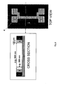
- Figure 3 illustrates the patterning (dry etching) of the temporary pattern into the first dielectric layer with preferably simultaneously converting the sidewalls of said temporary pattern such that they become etchable by an etchant. If needed an extra resist ash/strip step is performed to remove any photolithographic residues.
- Figure 4 illustrates the deposition of a second dielectric layer such that the temporary pattern is completely filled with said second dielectric material (also referred to as dielectric fill).
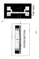
- Figure 5 illustrates the removal of part of the second dielectric layer (also referred to as planarization) such that the upper level of said second dielectric layer equals the level of said first dielectric layer. This step can be done by chemical mechanical polishing or etchback (wet or dry).
- Figure 6 illustrates the (optional) bond pad clear out step.
- Cross-section 2 of Figure 6 clearly shows the clear out of the bond pads creating open structures at both ends of the (narrow) trenches.
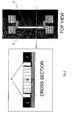
- Figure 7 illustrates the selective etch process used to remove the damaged part of the first dielectric material such that very small or narrow trenches are created.
- Figure 8 illustrates the deposition of a barrier layer (and optionally a seed layer) onto the sidewalls of said narrow trenches.
- Figure 9 illustrates the deposition of copper (e.g plating) within the narrow trenches.
- the present invention provides a method for the production of narrow trenches in a semiconductor device. More specifically a method is disclosed to produce narrow trenches having a width smaller than 50 nm and more preferred having a width of 20 nm to 30 nm and an aspect ratio of 10 to 2 (ratio of depth versus width) and more preferred having an aspect ratio of 10 to 1.
- narrow trenches are based on chemically changing the properties of a first dielectricum locally, such that part of said first dielectricum is chemically altered and becomes etchable by an etchant.
- a temporary pattern is created in said first dielectricum.
- Said temporary structure is defined by photolithographic patterning and is having a non-critical design, parts of this structure will be used to create the narrow trenches of the present invention.
- the sidewalls of said temporary pattern are damaged and/or converted such that these sidewalls become etchable by a first etching substance.
- a second dielectricum is deposited and if necessary planarized such that its upper level equals the level of the first dielectricum.
- Said planarizing step can be chemical mechanical planarization (CMP) or etchback.
- the conversion (preferably an oxidation step) within said first dielectricum can be established during the patterning of the temporary structure (done by anisotropic dry etching) in an oxygen containing plasma or ex-situ by introducing an oxidizing step e.g. UV/ozone treatment or supercritical carbon-dioxide with addition of an oxidizer.
- an oxidizing step e.g. UV/ozone treatment or supercritical carbon-dioxide with addition of an oxidizer.
- the method according to the invention for the production of narrow trenches used for interconnects in a semiconductor device is illustrated in Figures 2 to 7.
- the method starts with the deposition of an etchstop layer 1 onto a substrate.
- Said substrate can be a Si wafer comprising active devices or any substrate suitable for semiconductor processing.
- Said etch stop layer can be SiC, SiN, etc.
- a first dielectric layer 2 will be deposited onto said etchstop layer 1 .
- the thickness of said layer will determine the depth of the narrow trenches created by this invention, if narrow trenches having a width of 20 nm to 40 nm are aimed, the thickness of the deposited first dielectric layer is preferably comprised between 200 nm and 400 nm such that aspect ratios of 10 to 2 or even 10 to 1 can be obtained in the final fabricated trenches.
- the deposition of said first dielectric material 2 can be performed by a method such as for instance Plasma Enhanced Chemical Vapour Deposition (PE-CVD), Chemical Vapour Deposition (CVD), spin-on deposition etc.
- PE-CVD Plasma Enhanced Chemical Vapour Deposition
- CVD Chemical Vapour Deposition
- said first dielectric material 2 are the Organo Silicate Glass (OSG), (hydrogenated) silicon oxycarbides which are also commonly referred to as SiOC(H) materials, or Carbon doped oxides (including higher porosity derivatives). Examples of these materials are commercially available materials such as ® Black Diamond (referred to as BD), ® Coral or ® Aurora.
- a temporary structure will be patterned.
- photosensitive layers 3 (comprising at least a resist and anti-reflective coating) will be deposited onto said first dielectric layer 2 and the temporary pattern will be transferred into said photosensitive layers 3 by photolithographic processing.
- dry etch patterning the temporary pattern will be transferred into said first dielectric layer 2.
- the remaining resist and polymers (not shown) are then removed by a combination of dry ash plasma and wet strip.
- a (metal) hardmask layer deposited (situated in between said first dielectric layer and photosensitive layer) to facilitate the dry etch processing.
- the sidewalls of said temporary pattern in said first dielectric layer 2 need to be converted (also referred to in this application as "damage") such that they become etchable by an etchant.
- the conversion of the first dielectric material 2 into converted dielectric material 4 can be performed in-situ (simultaneously) during the dry etching (patterning) of the first dielectric material 2 and/or ashing using an oxidizing plasma.
- the conversion of the first dielectric material 2 into converted/damaged dielectric material 4 can be also ex-situ by performing an additional (oxidizing) treatment to the first dielectric material 2 after the dry etching of the first dielectric material 2 such as UV-ozone treatment, Super Critical CO 2 (SCCO 2 ) with addition of an oxidizer.
- an additional (oxidizing) treatment to the first dielectric material 2 after the dry etching of the first dielectric material 2
- UV-ozone treatment such as UV-ozone treatment, Super Critical CO 2 (SCCO 2 ) with addition of an oxidizer.
- SCCO 2 Super Critical CO 2
- the conversion leads to a reduced carbon concentration in the converted dielectric 4 as compared to original first dielectric material 2.
- the converted dielectric material 4 is a carbon depleted SiCO(H) material.
- the extent of the conversion of the first dielectric material 2 into converted dielectric material 4 is depending on the type of SiCO(H) material, more specifically on the porosity and carbon content of the first dielectric material 2.
- they are also referred to as SiO x material.
- a SiO x film corresponds to a Si (silicon) and O (oxygen) containing film, where both elements are not stoichiometrically related. This sort of film has typically more defects and is less cross-linked as compared to a SiO 2 one. Because the SiO x material is less cross-linked it is more susceptible to HF etching (removal process).
- the temporary pattern comprising the converted/damaged sidewalls is illustrated in Figure 3, the front view and top view of the structure show clearly the dimensions of the damaged areas 4 towards the undamaged areas 2.
- a second dielectric layer 5 made of a second dielectric material is then deposited within said temporary structure.
- Said second dielectric material can be identical to the first dielectric material 2 but not preferred.
- Preferably said second dielectric material 5 is a spin-on dielectricum that can be deposited very conformal and is able to fill the temporary structure completely.
- An example of said spin-on dielectric low-k materials (i.e. k value lower than 3,9) is commercially available LKD ® from JSR, Zirkon ® from Shipley, NCS ® from CCIC, etc.
- the overburden of said second dielectric material 5 will be removed such that the upper level of said second dielectric layer 5 equals the level of said first dielectric layer 2.
- the removal process also referred to as planarization, can be performed by chemical mechanical polishing or etchback (wet or dry).
- etchback wet or dry.
- the resulting structure top view and side view is shown in Figure 5.
- the damaged/converted part 4 of the first dielectric layer 2 is removed by means of a selective etch process which removes the damaged/converted part in said first dielectric layer 2 with an etchant such that narrow trenches 6 are created.
- the resulting structure comprising the narrow trenches 6 is illustrated in Figure 7.
- said "selective" etching is preferably a wet etching and said etchant preferably comprises HF.
- Said first etchant composition can comprise less than (about) 5 wt.% HF, preferably less than (about) 2 wt.% HF and more preferably (about) 1 wt.% HF.
- Said selective etching can also be a dry etching process. Preferably this selective etching is performed by dipping the structures in an aqueous solution comprising HF.
- said first dielectric material 2 and second dielectric material 5 must be resistant to said etchant.
- the patterning (dry etching) of the temporary structure in said first dielectric layer 2 can be performed by an oxidizing plasma, wherein said plasma may comprise oxygen and may further comprise an (hydro)fluorocarbon compound.
- said converted dielectric material 4 has preferably in-plane dimensions smaller than 50 nm and most preferred of about 20 nm to 40 nm.
- the trenches as described in this invention are preferably part of a (dual) damascene structure in the back end of line (BEOL) of a semiconductor device or can be used as interconnect structures in the BEOL.
- BEOL back end of line
- trenches as described in this invention are preferably used to study and optimize barrier layer, seed layer and/or copper deposition processes within narrow trenches.
- Figure 8 illustrates the deposition of a barrier layer 7 (and optionally a seed layer) within said narrow trenches.
- Figure 9 illustrates the deposition of conductive material 8 (e.g. copper deposition by plating processes) within the narrow trenches.
- conductive material 8 e.g. copper deposition by plating processes
- the planarization steps needed to remove the overburden of material (barrier layer and/or copper) are not shown in the Figures.
Landscapes
- Engineering & Computer Science (AREA)
- Physics & Mathematics (AREA)
- Geometry (AREA)
- Manufacturing & Machinery (AREA)
- Microelectronics & Electronic Packaging (AREA)
- Internal Circuitry In Semiconductor Integrated Circuit Devices (AREA)
- Chemically Coating (AREA)
Abstract
Description
- The present invention is related to the field of semiconductor processing.
- More specifically it is related to the production of micro and nano-electromechanical systems and to the production of low dielectric isolation for interconnects. It contributes to the exploration of the field of narrow trenches in semiconductor devices.
- Interconnects have been, are, and will continue to be a limiting factor for the performance and cost of integrated circuits. As technology scales down further, the problems associated with interconnects become ever more pressing. The introduction of low-resistive copper as an alternative interconnect material for aluminum presents researchers with some new challenges, since copper cannot be implemented in the same manner as aluminum alloys.
- As feature sizes shrink, narrower copper trenches need to be formed. Also to facilitate closer packing and multilevel connections, trenches are getting proportionally deeper as they get narrower. These deep trenches etched into the dielectric must be filled completely, without voids or defects. With current technology, the deeper the trench, the more likely there will be defects.
- "Dual-Damascene" methods are currently used to etch the trenches, fill them electrolytically, then mechanically polish away the excess metal using a chemically active slurry. Etching and filling narrow structures with high aspect ratios will be especially difficult for dual-Damascene architectures.
- The challenge is to address narrower trenches, the goal is to get down to a width of these trenches of about 20 to 30 nm, with an aspect ratio of 10 to 1 (ratio length to width).
- The Semiconductor Industry Association's most recent National Technology Roadmap predicts that new lithography methods will be able to go as far as a trench width of 50 nm to 60 nm with an aspect ratio of 3 to 1 by 2006.
- Because currently used damascene techniques to fill future narrow trenches, barrier deposition techniques such as ALD and CVD are not straight forward in these small trenches (having a width of 20-30 nm and aspect ratio of 10 to 1) it would be very helpful to have an alternative patterning method or at least a test structure available for these narrow trenches.
- A method is disclosed for the production of narrow trenches in a semiconductor device. More specifically a method is disclosed to produce one or more narrow trenches, said narrow trench(es) having a width smaller than 40 nm, preferably comprised between 20 nm and 30 nm and having an aspect ratio (ratio of depth versus width) preferably comprised between (about) 10 and (about) 2, more preferably comprised between (about) 10 and (about) 1.
- To fabricate said narrow trenches first a temporary structure is patterned within a first dielectric layer (preferably SiCO(H) such as Black Diamond®).
- Said temporary structure is defined by photolithographic patterning and is having a non-critical design, parts of this structure however will be used to create the narrow trenches of the present invention.
- During etching of said temporary structure, the sidewalls of said temporary pattern are damaged and/or chemically converted. More specifically the sidewalls of the temporary pattern in said first dielectric material are damaged in a controlled way e.g. by choosing the right selectivity of plasma used during patterning of said temporary structure or alternatively by performing an extra conversion step such as chemical oxidation of the sidewalls. Said damage is such that the damaged portion becomes etchable by an etchant, preferably said etchant comprises HF (fluoridric acid), more preferred less than 5% HF and most preferred about 1% HF.
- A second dielectric material is then deposited within the temporary structure and the overburden of said second dielectric material is removed until it reaches the upper level of the first dielectric material (etchback or CMP). Said second dielectric material can be a SiCO(H) dielectric material deposited by CVD (identical or not identical to the first dielectric material) but is preferably a spin-on dielectric low-k material (i.e. k value lower than 3,9) such as LKD® commercially available from JSR, Zirkon® commercially available from Shipley, NCS® commercially available from CCIC, etc.
- Subsequently an etch process is used to remove the damaged part of the first dielectric material such that very small or narrow trenches are created. Said etch process must be selective towards the damaged portion of the first dielectric material.
- Said narrow trenches are characterized as trenches having a width smaller than 50 nm, preferably comprised between 20 nm and 30 nm and having an aspect ratio (ratio of depth versus width) of 10 to 2 or even more preferred of 10 to 1.
- Said narrow trenches can be used as test vehicle to study and optimize barrier deposition, copper plating and seedlayer deposition within very small trenches (10-30 nm width).
- The present invention provides a method for making narrow trenches within a dielectric material, comprising the steps of:
- depositing an etchstop layer onto a substrate
- depositing a first dielectric layer on top of said etchstop layer,
- patterning a temporary pattern in said first dielectric layer,
- damaging (or converting) the sidewalls of said temporary pattern such that they become etchable by an etchant,
- depositing a second dielectric layer within said temporary structure,
- removing the overburden of said second dielectric material such that the upper level of said second dielectric layer equals the level of said first dielectric layer,
- selectively removing the damaged part in said first dielectric layer with an etchant such that narrow trenches are created.
- In a method according to the invention said narrow trenches preferably have a width smaller than 50 nm, more preferably smaller than 40 nm and most preferred smaller than 30 nm.
- Preferably, the width of said trenches is comprised between (about) 50 nm and (about) 10 nm, more preferably between (about) 40 nm and (about) 20 nm, and even more preferably between (about) 30 nm and (about) 20 nm.
- Preferably, the aspect ratio varies from (about) 10 to (about) 2 and even more preferred from (about) 10 to (about) 1.
- In a method according to the invention, said "selective" etching is preferably a wet etching and said etchant preferably comprises HF. Said first etchant composition can comprise less than (about) 5 wt.% HF, preferably less than (about) 2 wt.% HF and more preferably (about) 1 wt.% HF. Said selective etching can also be a dry etching process.
- In a method according to the invention, said first and second dielectric material must be resistant to said etchant.
- In a method according to the invention, the patterning of the temporary structure in said first dielectric layer can be performed by an oxidizing plasma, wherein said plasma may comprise oxygen and may further comprise an (hydro)fluorocarbon compound.
- In a method according to the invention, the step of patterning the temporary pattern and damaging the sidewalls of said temporary structure are performed simultaneously.
- Alternatively, the sidewalls can also be damaged in a separate process step.
- The present invention also provides a method for making a semiconductor device comprising the steps of a method of the invention for making narrow trenches.
- The present invention also provides a device obtainable by a method of the invention comprising narrow trenches. Said narrow trenches preferably have a width smaller than 50 nm, more preferably smaller than 40 nm and most preferred smaller than 30 nm. More specifically, the width of said narrow trenches is comprised between (about) 50 nm and (about) 10 nm, preferably between (about) 40 nm and (about) 20 nm and more preferably between (about) 30 nm and (about) 20 nm. The aspect ratio of said narrow trenches varies from (about) 10 to (about) 2 and more preferred from (about) 10 to (about) 1.
- All figures/drawings are intended to illustrate some aspects and embodiments of the present invention. Devices are depicted in a simplified way for reason of clarity. Not all alternatives and options are shown and therefore the invention is not limited to the content of the given drawings. Like numerals are employed to reference like parts in the different figures.
- Figure 1 (PRIOR ART) illustrates trenches conform state of the art technology with minimum width of 50 nm to 60 nm and aspect ratios of 3 to 1.
- Figures 2 to 7 illustrate the different processing steps of the method according to the present invention to form narrow trenches.
- Figure 2 illustrates the photolithographic patterning of the temporary pattern.
- Figure 3 illustrates the patterning (dry etching) of the temporary pattern into the first dielectric layer with preferably simultaneously converting the sidewalls of said temporary pattern such that they become etchable by an etchant. If needed an extra resist ash/strip step is performed to remove any photolithographic residues.
- Figure 4 illustrates the deposition of a second dielectric layer such that the temporary pattern is completely filled with said second dielectric material (also referred to as dielectric fill).
- Figure 5 illustrates the removal of part of the second dielectric layer (also referred to as planarization) such that the upper level of said second dielectric layer equals the level of said first dielectric layer. This step can be done by chemical mechanical polishing or etchback (wet or dry).
- Figure 6 illustrates the (optional) bond pad clear out step.
Cross-section 2 of Figure 6 clearly shows the clear out of the bond pads creating open structures at both ends of the (narrow) trenches. - Figure 7 illustrates the selective etch process used to remove the damaged part of the first dielectric material such that very small or narrow trenches are created.
- Figure 8 illustrates the deposition of a barrier layer (and optionally a seed layer) onto the sidewalls of said narrow trenches.
- Figure 9 illustrates the deposition of copper (e.g plating) within the narrow trenches.
- The present invention provides a method for the production of narrow trenches in a semiconductor device. More specifically a method is disclosed to produce narrow trenches having a width smaller than 50 nm and more preferred having a width of 20 nm to 30 nm and an aspect ratio of 10 to 2 (ratio of depth versus width) and more preferred having an aspect ratio of 10 to 1.
- The formation of narrow trenches is based on chemically changing the properties of a first dielectricum locally, such that part of said first dielectricum is chemically altered and becomes etchable by an etchant.
- Preferably first a temporary pattern is created in said first dielectricum. Said temporary structure is defined by photolithographic patterning and is having a non-critical design, parts of this structure will be used to create the narrow trenches of the present invention. The sidewalls of said temporary pattern are damaged and/or converted such that these sidewalls become etchable by a first etching substance.
- Within said temporary pattern a second dielectricum is deposited and if necessary planarized such that its upper level equals the level of the first dielectricum. Said planarizing step can be chemical mechanical planarization (CMP) or etchback.
- The conversion (preferably an oxidation step) within said first dielectricum can be established during the patterning of the temporary structure (done by anisotropic dry etching) in an oxygen containing plasma or ex-situ by introducing an oxidizing step e.g. UV/ozone treatment or supercritical carbon-dioxide with addition of an oxidizer.
- The method according to the invention for the production of narrow trenches used for interconnects in a semiconductor device is illustrated in Figures 2 to 7. The method starts with the deposition of an
etchstop layer 1 onto a substrate. Said substrate can be a Si wafer comprising active devices or any substrate suitable for semiconductor processing. Said etch stop layer can be SiC, SiN, etc. - Subsequently a first
dielectric layer 2 will be deposited onto saidetchstop layer 1. The thickness of said layer will determine the depth of the narrow trenches created by this invention, if narrow trenches having a width of 20 nm to 40 nm are aimed, the thickness of the deposited first dielectric layer is preferably comprised between 200 nm and 400 nm such that aspect ratios of 10 to 2 or even 10 to 1 can be obtained in the final fabricated trenches. - The deposition of said first
dielectric material 2 can be performed by a method such as for instance Plasma Enhanced Chemical Vapour Deposition (PE-CVD), Chemical Vapour Deposition (CVD), spin-on deposition etc. Examples of said firstdielectric material 2 are the Organo Silicate Glass (OSG), (hydrogenated) silicon oxycarbides which are also commonly referred to as SiOC(H) materials, or Carbon doped oxides (including higher porosity derivatives). Examples of these materials are commercially available materials such as ®Black Diamond (referred to as BD), ®Coral or ®Aurora. - In said first dielectric layer a temporary structure will be patterned. To achieve this, photosensitive layers 3 (comprising at least a resist and anti-reflective coating) will be deposited onto said first
dielectric layer 2 and the temporary pattern will be transferred into saidphotosensitive layers 3 by photolithographic processing. By means of dry etch patterning the temporary pattern will be transferred into said firstdielectric layer 2. The remaining resist and polymers (not shown) are then removed by a combination of dry ash plasma and wet strip. - If needed there can be additionally a (metal) hardmask layer deposited (situated in between said first dielectric layer and photosensitive layer) to facilitate the dry etch processing.
- The sidewalls of said temporary pattern in said first
dielectric layer 2 need to be converted (also referred to in this application as "damage") such that they become etchable by an etchant. - The conversion of the first
dielectric material 2 into converteddielectric material 4 can be performed in-situ (simultaneously) during the dry etching (patterning) of the firstdielectric material 2 and/or ashing using an oxidizing plasma. - The conversion of the first
dielectric material 2 into converted/damageddielectric material 4 can be also ex-situ by performing an additional (oxidizing) treatment to the firstdielectric material 2 after the dry etching of the firstdielectric material 2 such as UV-ozone treatment, Super Critical CO2 (SCCO2) with addition of an oxidizer. Several other oxidizing treatments are applicable to oxidize thedielectric material 2. - In case the first
dielectric material 2 is e.g. a SiCO(H) material such as Black Diamond, the conversion leads to a reduced carbon concentration in the converted dielectric 4 as compared to original firstdielectric material 2. The converteddielectric material 4 is a carbon depleted SiCO(H) material. The extent of the conversion of the firstdielectric material 2 into converteddielectric material 4 is depending on the type of SiCO(H) material, more specifically on the porosity and carbon content of the firstdielectric material 2. In case of complete carbon removal out of the SiCO(H) material, they are also referred to as SiOx material. A SiOx film corresponds to a Si (silicon) and O (oxygen) containing film, where both elements are not stoichiometrically related. This sort of film has typically more defects and is less cross-linked as compared to a SiO2 one. Because the SiOx material is less cross-linked it is more susceptible to HF etching (removal process). - The temporary pattern comprising the converted/damaged sidewalls is illustrated in Figure 3, the front view and top view of the structure show clearly the dimensions of the damaged
areas 4 towards theundamaged areas 2. - A
second dielectric layer 5 made of a second dielectric material is then deposited within said temporary structure. Said second dielectric material can be identical to the firstdielectric material 2 but not preferred. Preferably said seconddielectric material 5 is a spin-on dielectricum that can be deposited very conformal and is able to fill the temporary structure completely. An example of said spin-on dielectric low-k materials (i.e. k value lower than 3,9) is commercially available LKD® from JSR, Zirkon® from Shipley, NCS® from CCIC, etc. - If needed the overburden of said second
dielectric material 5 will be removed such that the upper level of said seconddielectric layer 5 equals the level of said firstdielectric layer 2. The removal process, also referred to as planarization, can be performed by chemical mechanical polishing or etchback (wet or dry). The resulting structure (top view and side view) is shown in Figure 5. - If needed there is a clear out of the bond pads, this is shown in Figure 6. Said bond pads are needed if electrical measurements and/or reliability studies are required to evaluate the quality of the narrow trenches (after filling them with conductive material). To perform the bond pad clear out a second photolithographic pattern is transferred into the
second dielectric layer 5 stopping on theetchstop layer 1. The removal of the second dielectric material in said bond pads can be achieved by anisotropically etching. The second cross-section of Figure 6 clearly shows the clear out of the bond pads creating open structures at both ends of the (narrow) trenches. - Finally the damaged/converted
part 4 of the firstdielectric layer 2 is removed by means of a selective etch process which removes the damaged/converted part in said firstdielectric layer 2 with an etchant such thatnarrow trenches 6 are created. The resulting structure comprising thenarrow trenches 6 is illustrated in Figure 7. - In a method according to the invention, said "selective" etching is preferably a wet etching and said etchant preferably comprises HF. Said first etchant composition can comprise less than (about) 5 wt.% HF, preferably less than (about) 2 wt.% HF and more preferably (about) 1 wt.% HF. Said selective etching can also be a dry etching process. Preferably this selective etching is performed by dipping the structures in an aqueous solution comprising HF.
- In a method according to the invention, said first
dielectric material 2 and seconddielectric material 5 must be resistant to said etchant. - In a method according to the invention, the patterning (dry etching) of the temporary structure in said first
dielectric layer 2 can be performed by an oxidizing plasma, wherein said plasma may comprise oxygen and may further comprise an (hydro)fluorocarbon compound. - In a method according to the invention said converted
dielectric material 4 has preferably in-plane dimensions smaller than 50 nm and most preferred of about 20 nm to 40 nm. - The trenches as described in this invention are preferably part of a (dual) damascene structure in the back end of line (BEOL) of a semiconductor device or can be used as interconnect structures in the BEOL.
- The trenches as described in this invention are preferably used to study and optimize barrier layer, seed layer and/or copper deposition processes within narrow trenches.
- Figure 8 illustrates the deposition of a barrier layer 7 (and optionally a seed layer) within said narrow trenches.
- Figure 9 illustrates the deposition of conductive material 8 (e.g. copper deposition by plating processes) within the narrow trenches. The planarization steps needed to remove the overburden of material (barrier layer and/or copper) are not shown in the Figures.
Claims (17)
- A method for making trenches having a width smaller than 40 nm , comprising the steps of:- depositing an etchstop layer (1) onto a substrate,- depositing a first dielectric layer (2) on top of said etchstop layer (1),- patterning a temporary structure in said first dielectric layer (2),- damaging or converting the sidewalls of said temporary patterned structure such that they become etchable by an etchant,- depositing a second dielectric layer (5) within said temporary structure,- removing the overburden of said second dielectric material (5) such that the upper level of said second dielectric layer equals the level of said first dielectric layer (2), and- selectively removing the damaged or converted part (4) in said first dielectric layer with an etchant such that narrow trenches are created,wherein the first and second dielectric materials are resistant to said etchant.
- The method for making trenches according to claim 1
wherein the step of patterning a temporary structure comprises the steps of:- depositing photosensitive layers (3) onto said first dielectric layer (2),- transferring said temporary structure into said photosensitive layers (3) lithographically, and- subsequently transferring said temporary structure into said first dielectric layer (2) by dry-etching. - The method for making trenches according to claim 1 or 2 wherein a hardmask or a metal hardmask is deposited on top of said first dielectric material (2).
- The method for making trenches according to any of claims 1 to 3 wherein the steps of patterning the temporary structure and damaging or converting the sidewalls of said temporary structure are performed simultaneously.
- The method for making trenches according to claim 4 wherein the steps of patterning the temporary structure and damaging or converting the sidewalls of said temporary structure are performed by an oxidizing plasma.
- The method for making trenches according to claim 5 wherein said plasma comprises oxygen.
- The method for making trenches according to claim 5 or 6, wherein said plasma further comprises one or more (hydro)fluorocarbon compounds.
- The method for making trenches according to any of claims 1 to 7, wherein said etchant is a wet etchant comprising HF.
- The method for making trenches according to any of claims 1 to 8, wherein said etchant comprises less than 5 wt.% HF.
- The method for making trenches according to any of claims 1 to 9 wherein said first dielectric material (2) is a SiCO(H) material.
- The method for making trenches according to any of claims 1 to 10 wherein said second dielectric material (5) is a spin-on low-k material.
- The method for making trenches according to any of claims 1 to 11 wherein the step of damaging or converting the sidewalls of the temporary structure is performed by an UV/ozone treatment with addition of an oxidizer or by a SCCO2 treatment with addition of an oxidizer.
- The method for making narrow trenches according to any of claims 1 to 12 wherein said damaged or converted portion of the first dielectric material (4) has in-plane dimensions smaller than 50 nm.
- The method for making trenches according to any of claims 1 to 13 wherein said narrow trenches have an aspect ratio of 10 to 1.
- The method for making trenches according to any of claims 1 to 14 further comprising the steps of:- depositing a barrier layer (7) within said trenches,- optionally, depositing a seed layer onto said barrier layer, and- depositing a conductive material (8) onto said seed layer or barrier layer to create completely filled trenches.
- A method for making a semiconductor device having trenches the width of which is less than 40 nm, comprising a method according to any of claims 1 to 15.
- A semiconductor device obtainable by a method according to any of claims 1 to 16, comprising trenches the width of which is less than 40 nm.
Priority Applications (1)
| Application Number | Priority Date | Filing Date | Title |
|---|---|---|---|
| JP2006248121A JP5214866B2 (en) | 2005-09-16 | 2006-09-13 | Method for forming narrow trenches in dielectric materials |
Applications Claiming Priority (1)
| Application Number | Priority Date | Filing Date | Title |
|---|---|---|---|
| US71806205P | 2005-09-16 | 2005-09-16 |
Publications (3)
| Publication Number | Publication Date |
|---|---|
| EP1764830A2 true EP1764830A2 (en) | 2007-03-21 |
| EP1764830A3 EP1764830A3 (en) | 2009-02-18 |
| EP1764830B1 EP1764830B1 (en) | 2012-01-25 |
Family
ID=37574965
Family Applications (1)
| Application Number | Title | Priority Date | Filing Date |
|---|---|---|---|
| EP05447238A Expired - Lifetime EP1764830B1 (en) | 2005-09-16 | 2005-10-21 | A method to create narrow trenches in dielectric materials |
Country Status (3)
| Country | Link |
|---|---|
| US (1) | US7560357B2 (en) |
| EP (1) | EP1764830B1 (en) |
| AT (1) | ATE543210T1 (en) |
Families Citing this family (3)
| Publication number | Priority date | Publication date | Assignee | Title |
|---|---|---|---|---|
| US20070085208A1 (en) * | 2005-10-13 | 2007-04-19 | Feng-Yu Hsu | Interconnect structure |
| US11037792B2 (en) | 2018-10-25 | 2021-06-15 | Taiwan Semiconductor Manufacturing Company Ltd. | Semiconductor structure etching solution and method for fabricating a semiconductor structure using the same etching solution |
| US11050012B2 (en) * | 2019-04-01 | 2021-06-29 | Taiwan Semiconductor Manufacturing Co., Ltd. | Method to protect electrodes from oxidation in a MEMS device |
Family Cites Families (9)
| Publication number | Priority date | Publication date | Assignee | Title |
|---|---|---|---|---|
| US5310626A (en) * | 1993-03-01 | 1994-05-10 | Motorola, Inc. | Method for forming a patterned layer using dielectric materials as a light-sensitive material |
| US5780340A (en) * | 1996-10-30 | 1998-07-14 | Advanced Micro Devices, Inc. | Method of forming trench transistor and isolation trench |
| TW334614B (en) * | 1997-03-04 | 1998-06-21 | Winbond Electronics Corp | The method of forming shallow trench isolation |
| US6242336B1 (en) * | 1997-11-06 | 2001-06-05 | Matsushita Electronics Corporation | Semiconductor device having multilevel interconnection structure and method for fabricating the same |
| US6388303B1 (en) * | 1999-04-21 | 2002-05-14 | Sanyo Electric Co., Ltd. | Semiconductor device and semiconductor device manufacture method |
| JP2002289683A (en) * | 2001-03-28 | 2002-10-04 | Nec Corp | Method of forming trench isolation structure and semiconductor device |
| KR100473733B1 (en) * | 2002-10-14 | 2005-03-10 | 매그나칩 반도체 유한회사 | Semiconductor device and method for manufacturing the same |
| JP4864307B2 (en) * | 2003-09-30 | 2012-02-01 | アイメック | Method for selectively forming an air gap and apparatus obtained by the method |
| DE102004005506B4 (en) * | 2004-01-30 | 2009-11-19 | Atmel Automotive Gmbh | Method of producing semiconductor active layers of different thickness in an SOI wafer |
-
2005
- 2005-10-21 AT AT05447238T patent/ATE543210T1/en active
- 2005-10-21 EP EP05447238A patent/EP1764830B1/en not_active Expired - Lifetime
-
2006
- 2006-09-15 US US11/532,190 patent/US7560357B2/en not_active Expired - Fee Related
Also Published As
| Publication number | Publication date |
|---|---|
| ATE543210T1 (en) | 2012-02-15 |
| US7560357B2 (en) | 2009-07-14 |
| EP1764830A3 (en) | 2009-02-18 |
| EP1764830B1 (en) | 2012-01-25 |
| US20070066028A1 (en) | 2007-03-22 |
Similar Documents
| Publication | Publication Date | Title |
|---|---|---|
| US7871923B2 (en) | Self-aligned air-gap in interconnect structures | |
| US7754601B2 (en) | Semiconductor interconnect air gap formation process | |
| US6713402B2 (en) | Methods for polymer removal following etch-stop layer etch | |
| US7319274B2 (en) | Methods for selective integration of airgaps and devices made by such methods | |
| CN100576494C (en) | Method for forming dual damascene wiring of semiconductor device using protective via capping layer | |
| US7470616B1 (en) | Damascene wiring fabrication methods incorporating dielectric cap etch process with hard mask retention | |
| US20080146029A1 (en) | Method of forming an interconnect structure | |
| US20060246717A1 (en) | Method for fabricating a dual damascene and polymer removal | |
| JP5186086B2 (en) | Dual damascene patterning approach | |
| EP1351290A2 (en) | Methods for forming vias and trenches with controlled SiC etch rate and selectivity | |
| US7670947B2 (en) | Metal interconnect structure and process for forming same | |
| US6265307B1 (en) | Fabrication method for a dual damascene structure | |
| US7056821B2 (en) | Method for manufacturing dual damascene structure with a trench formed first | |
| US6319820B1 (en) | Fabrication method for dual damascene structure | |
| EP1764830B1 (en) | A method to create narrow trenches in dielectric materials | |
| JP4523351B2 (en) | Manufacturing method of semiconductor device | |
| JP5047504B2 (en) | Method for manufacturing dual damascene wiring of semiconductor device using via capping protective film | |
| CN111599748A (en) | Method for manufacturing interconnection structure | |
| JP5214866B2 (en) | Method for forming narrow trenches in dielectric materials | |
| EP1646083B1 (en) | Alternative dual damascene patterning approach | |
| JP2005203429A (en) | Manufacturing method of semiconductor device | |
| US20060148244A1 (en) | Method for cleaning a semiconductor substrate | |
| KR101036159B1 (en) | Metal wiring formation method using dual damascene method | |
| CN115472491A (en) | Method of fabricating a semiconductor structure | |
| JP2000114375A (en) | Method for manufacturing semiconductor device |
Legal Events
| Date | Code | Title | Description |
|---|---|---|---|
| PUAI | Public reference made under article 153(3) epc to a published international application that has entered the european phase |
Free format text: ORIGINAL CODE: 0009012 |
|
| AK | Designated contracting states |
Kind code of ref document: A2 Designated state(s): AT BE BG CH CY CZ DE DK EE ES FI FR GB GR HU IE IS IT LI LT LU LV MC NL PL PT RO SE SI SK TR |
|
| AX | Request for extension of the european patent |
Extension state: AL BA HR MK YU |
|
| PUAL | Search report despatched |
Free format text: ORIGINAL CODE: 0009013 |
|
| AK | Designated contracting states |
Kind code of ref document: A3 Designated state(s): AT BE BG CH CY CZ DE DK EE ES FI FR GB GR HU IE IS IT LI LT LU LV MC NL PL PT RO SE SI SK TR |
|
| AX | Request for extension of the european patent |
Extension state: AL BA HR MK YU |
|
| 17P | Request for examination filed |
Effective date: 20090610 |
|
| RAP1 | Party data changed (applicant data changed or rights of an application transferred) |
Owner name: IMEC |
|
| AKX | Designation fees paid |
Designated state(s): AT BE BG CH CY CZ DE DK EE ES FI FR GB GR HU IE IS IT LI LT LU LV MC NL PL PT RO SE SI SK TR |
|
| GRAP | Despatch of communication of intention to grant a patent |
Free format text: ORIGINAL CODE: EPIDOSNIGR1 |
|
| GRAS | Grant fee paid |
Free format text: ORIGINAL CODE: EPIDOSNIGR3 |
|
| GRAA | (expected) grant |
Free format text: ORIGINAL CODE: 0009210 |
|
| AK | Designated contracting states |
Kind code of ref document: B1 Designated state(s): AT BE BG CH CY CZ DE DK EE ES FI FR GB GR HU IE IS IT LI LT LU LV MC NL PL PT RO SE SI SK TR |
|
| REG | Reference to a national code |
Ref country code: GB Ref legal event code: FG4D |
|
| REG | Reference to a national code |
Ref country code: CH Ref legal event code: EP |
|
| REG | Reference to a national code |
Ref country code: AT Ref legal event code: REF Ref document number: 543210 Country of ref document: AT Kind code of ref document: T Effective date: 20120215 |
|
| REG | Reference to a national code |
Ref country code: IE Ref legal event code: FG4D |
|
| REG | Reference to a national code |
Ref country code: DE Ref legal event code: R096 Ref document number: 602005032370 Country of ref document: DE Effective date: 20120329 |
|
| REG | Reference to a national code |
Ref country code: NL Ref legal event code: VDEP Effective date: 20120125 |
|
| LTIE | Lt: invalidation of european patent or patent extension |
Effective date: 20120125 |
|
| PG25 | Lapsed in a contracting state [announced via postgrant information from national office to epo] |
Ref country code: LT Free format text: LAPSE BECAUSE OF FAILURE TO SUBMIT A TRANSLATION OF THE DESCRIPTION OR TO PAY THE FEE WITHIN THE PRESCRIBED TIME-LIMIT Effective date: 20120125 Ref country code: NL Free format text: LAPSE BECAUSE OF FAILURE TO SUBMIT A TRANSLATION OF THE DESCRIPTION OR TO PAY THE FEE WITHIN THE PRESCRIBED TIME-LIMIT Effective date: 20120125 Ref country code: BG Free format text: LAPSE BECAUSE OF FAILURE TO SUBMIT A TRANSLATION OF THE DESCRIPTION OR TO PAY THE FEE WITHIN THE PRESCRIBED TIME-LIMIT Effective date: 20120425 Ref country code: IS Free format text: LAPSE BECAUSE OF FAILURE TO SUBMIT A TRANSLATION OF THE DESCRIPTION OR TO PAY THE FEE WITHIN THE PRESCRIBED TIME-LIMIT Effective date: 20120525 Ref country code: BE Free format text: LAPSE BECAUSE OF FAILURE TO SUBMIT A TRANSLATION OF THE DESCRIPTION OR TO PAY THE FEE WITHIN THE PRESCRIBED TIME-LIMIT Effective date: 20120125 |
|
| PG25 | Lapsed in a contracting state [announced via postgrant information from national office to epo] |
Ref country code: GR Free format text: LAPSE BECAUSE OF FAILURE TO SUBMIT A TRANSLATION OF THE DESCRIPTION OR TO PAY THE FEE WITHIN THE PRESCRIBED TIME-LIMIT Effective date: 20120426 Ref country code: PL Free format text: LAPSE BECAUSE OF FAILURE TO SUBMIT A TRANSLATION OF THE DESCRIPTION OR TO PAY THE FEE WITHIN THE PRESCRIBED TIME-LIMIT Effective date: 20120125 Ref country code: PT Free format text: LAPSE BECAUSE OF FAILURE TO SUBMIT A TRANSLATION OF THE DESCRIPTION OR TO PAY THE FEE WITHIN THE PRESCRIBED TIME-LIMIT Effective date: 20120525 Ref country code: LV Free format text: LAPSE BECAUSE OF FAILURE TO SUBMIT A TRANSLATION OF THE DESCRIPTION OR TO PAY THE FEE WITHIN THE PRESCRIBED TIME-LIMIT Effective date: 20120125 Ref country code: FI Free format text: LAPSE BECAUSE OF FAILURE TO SUBMIT A TRANSLATION OF THE DESCRIPTION OR TO PAY THE FEE WITHIN THE PRESCRIBED TIME-LIMIT Effective date: 20120125 |
|
| REG | Reference to a national code |
Ref country code: AT Ref legal event code: MK05 Ref document number: 543210 Country of ref document: AT Kind code of ref document: T Effective date: 20120125 |
|
| PG25 | Lapsed in a contracting state [announced via postgrant information from national office to epo] |
Ref country code: CY Free format text: LAPSE BECAUSE OF FAILURE TO SUBMIT A TRANSLATION OF THE DESCRIPTION OR TO PAY THE FEE WITHIN THE PRESCRIBED TIME-LIMIT Effective date: 20120125 |
|
| PG25 | Lapsed in a contracting state [announced via postgrant information from national office to epo] |
Ref country code: EE Free format text: LAPSE BECAUSE OF FAILURE TO SUBMIT A TRANSLATION OF THE DESCRIPTION OR TO PAY THE FEE WITHIN THE PRESCRIBED TIME-LIMIT Effective date: 20120125 Ref country code: SE Free format text: LAPSE BECAUSE OF FAILURE TO SUBMIT A TRANSLATION OF THE DESCRIPTION OR TO PAY THE FEE WITHIN THE PRESCRIBED TIME-LIMIT Effective date: 20120125 Ref country code: DK Free format text: LAPSE BECAUSE OF FAILURE TO SUBMIT A TRANSLATION OF THE DESCRIPTION OR TO PAY THE FEE WITHIN THE PRESCRIBED TIME-LIMIT Effective date: 20120125 Ref country code: SI Free format text: LAPSE BECAUSE OF FAILURE TO SUBMIT A TRANSLATION OF THE DESCRIPTION OR TO PAY THE FEE WITHIN THE PRESCRIBED TIME-LIMIT Effective date: 20120125 Ref country code: RO Free format text: LAPSE BECAUSE OF FAILURE TO SUBMIT A TRANSLATION OF THE DESCRIPTION OR TO PAY THE FEE WITHIN THE PRESCRIBED TIME-LIMIT Effective date: 20120125 Ref country code: CZ Free format text: LAPSE BECAUSE OF FAILURE TO SUBMIT A TRANSLATION OF THE DESCRIPTION OR TO PAY THE FEE WITHIN THE PRESCRIBED TIME-LIMIT Effective date: 20120125 |
|
| PG25 | Lapsed in a contracting state [announced via postgrant information from national office to epo] |
Ref country code: IT Free format text: LAPSE BECAUSE OF FAILURE TO SUBMIT A TRANSLATION OF THE DESCRIPTION OR TO PAY THE FEE WITHIN THE PRESCRIBED TIME-LIMIT Effective date: 20120125 Ref country code: SK Free format text: LAPSE BECAUSE OF FAILURE TO SUBMIT A TRANSLATION OF THE DESCRIPTION OR TO PAY THE FEE WITHIN THE PRESCRIBED TIME-LIMIT Effective date: 20120125 |
|
| PLBE | No opposition filed within time limit |
Free format text: ORIGINAL CODE: 0009261 |
|
| STAA | Information on the status of an ep patent application or granted ep patent |
Free format text: STATUS: NO OPPOSITION FILED WITHIN TIME LIMIT |
|
| 26N | No opposition filed |
Effective date: 20121026 |
|
| PG25 | Lapsed in a contracting state [announced via postgrant information from national office to epo] |
Ref country code: AT Free format text: LAPSE BECAUSE OF FAILURE TO SUBMIT A TRANSLATION OF THE DESCRIPTION OR TO PAY THE FEE WITHIN THE PRESCRIBED TIME-LIMIT Effective date: 20120125 |
|
| REG | Reference to a national code |
Ref country code: DE Ref legal event code: R097 Ref document number: 602005032370 Country of ref document: DE Effective date: 20121026 |
|
| PG25 | Lapsed in a contracting state [announced via postgrant information from national office to epo] |
Ref country code: ES Free format text: LAPSE BECAUSE OF FAILURE TO SUBMIT A TRANSLATION OF THE DESCRIPTION OR TO PAY THE FEE WITHIN THE PRESCRIBED TIME-LIMIT Effective date: 20120506 |
|
| PG25 | Lapsed in a contracting state [announced via postgrant information from national office to epo] |
Ref country code: MC Free format text: LAPSE BECAUSE OF NON-PAYMENT OF DUE FEES Effective date: 20121031 |
|
| REG | Reference to a national code |
Ref country code: CH Ref legal event code: PL |
|
| REG | Reference to a national code |
Ref country code: IE Ref legal event code: MM4A |
|
| PG25 | Lapsed in a contracting state [announced via postgrant information from national office to epo] |
Ref country code: CH Free format text: LAPSE BECAUSE OF NON-PAYMENT OF DUE FEES Effective date: 20121031 Ref country code: IE Free format text: LAPSE BECAUSE OF NON-PAYMENT OF DUE FEES Effective date: 20121021 Ref country code: LI Free format text: LAPSE BECAUSE OF NON-PAYMENT OF DUE FEES Effective date: 20121031 |
|
| PG25 | Lapsed in a contracting state [announced via postgrant information from national office to epo] |
Ref country code: TR Free format text: LAPSE BECAUSE OF FAILURE TO SUBMIT A TRANSLATION OF THE DESCRIPTION OR TO PAY THE FEE WITHIN THE PRESCRIBED TIME-LIMIT Effective date: 20120125 |
|
| PG25 | Lapsed in a contracting state [announced via postgrant information from national office to epo] |
Ref country code: LU Free format text: LAPSE BECAUSE OF NON-PAYMENT OF DUE FEES Effective date: 20121021 |
|
| PG25 | Lapsed in a contracting state [announced via postgrant information from national office to epo] |
Ref country code: HU Free format text: LAPSE BECAUSE OF FAILURE TO SUBMIT A TRANSLATION OF THE DESCRIPTION OR TO PAY THE FEE WITHIN THE PRESCRIBED TIME-LIMIT Effective date: 20051021 |
|
| REG | Reference to a national code |
Ref country code: FR Ref legal event code: PLFP Year of fee payment: 12 |
|
| PGFP | Annual fee paid to national office [announced via postgrant information from national office to epo] |
Ref country code: GB Payment date: 20160928 Year of fee payment: 12 |
|
| PGFP | Annual fee paid to national office [announced via postgrant information from national office to epo] |
Ref country code: FR Payment date: 20160921 Year of fee payment: 12 |
|
| PGFP | Annual fee paid to national office [announced via postgrant information from national office to epo] |
Ref country code: DE Payment date: 20160922 Year of fee payment: 12 |
|
| REG | Reference to a national code |
Ref country code: DE Ref legal event code: R119 Ref document number: 602005032370 Country of ref document: DE |
|
| GBPC | Gb: european patent ceased through non-payment of renewal fee |
Effective date: 20171021 |
|
| REG | Reference to a national code |
Ref country code: FR Ref legal event code: ST Effective date: 20180629 |
|
| PG25 | Lapsed in a contracting state [announced via postgrant information from national office to epo] |
Ref country code: DE Free format text: LAPSE BECAUSE OF NON-PAYMENT OF DUE FEES Effective date: 20180501 Ref country code: GB Free format text: LAPSE BECAUSE OF NON-PAYMENT OF DUE FEES Effective date: 20171021 |
|
| PG25 | Lapsed in a contracting state [announced via postgrant information from national office to epo] |
Ref country code: FR Free format text: LAPSE BECAUSE OF NON-PAYMENT OF DUE FEES Effective date: 20171031 |