EP1764772A2 - Organic light emitting diode display device and method of operating the same - Google Patents
Organic light emitting diode display device and method of operating the same Download PDFInfo
- Publication number
- EP1764772A2 EP1764772A2 EP06254812A EP06254812A EP1764772A2 EP 1764772 A2 EP1764772 A2 EP 1764772A2 EP 06254812 A EP06254812 A EP 06254812A EP 06254812 A EP06254812 A EP 06254812A EP 1764772 A2 EP1764772 A2 EP 1764772A2
- Authority
- EP
- European Patent Office
- Prior art keywords
- data
- signal
- demultiplexer
- pixels
- scan
- Prior art date
- Legal status (The legal status is an assumption and is not a legal conclusion. Google has not performed a legal analysis and makes no representation as to the accuracy of the status listed.)
- Granted
Links
Images


Classifications
-
- G—PHYSICS
- G09—EDUCATION; CRYPTOGRAPHY; DISPLAY; ADVERTISING; SEALS
- G09G—ARRANGEMENTS OR CIRCUITS FOR CONTROL OF INDICATING DEVICES USING STATIC MEANS TO PRESENT VARIABLE INFORMATION
- G09G3/00—Control arrangements or circuits, of interest only in connection with visual indicators other than cathode-ray tubes
- G09G3/20—Control arrangements or circuits, of interest only in connection with visual indicators other than cathode-ray tubes for presentation of an assembly of a number of characters, e.g. a page, by composing the assembly by combination of individual elements arranged in a matrix no fixed position being assigned to or needed to be assigned to the individual characters or partial characters
- G09G3/22—Control arrangements or circuits, of interest only in connection with visual indicators other than cathode-ray tubes for presentation of an assembly of a number of characters, e.g. a page, by composing the assembly by combination of individual elements arranged in a matrix no fixed position being assigned to or needed to be assigned to the individual characters or partial characters using controlled light sources
- G09G3/30—Control arrangements or circuits, of interest only in connection with visual indicators other than cathode-ray tubes for presentation of an assembly of a number of characters, e.g. a page, by composing the assembly by combination of individual elements arranged in a matrix no fixed position being assigned to or needed to be assigned to the individual characters or partial characters using controlled light sources using electroluminescent panels
-
- G—PHYSICS
- G09—EDUCATION; CRYPTOGRAPHY; DISPLAY; ADVERTISING; SEALS
- G09G—ARRANGEMENTS OR CIRCUITS FOR CONTROL OF INDICATING DEVICES USING STATIC MEANS TO PRESENT VARIABLE INFORMATION
- G09G3/00—Control arrangements or circuits, of interest only in connection with visual indicators other than cathode-ray tubes
- G09G3/20—Control arrangements or circuits, of interest only in connection with visual indicators other than cathode-ray tubes for presentation of an assembly of a number of characters, e.g. a page, by composing the assembly by combination of individual elements arranged in a matrix no fixed position being assigned to or needed to be assigned to the individual characters or partial characters
- G09G3/22—Control arrangements or circuits, of interest only in connection with visual indicators other than cathode-ray tubes for presentation of an assembly of a number of characters, e.g. a page, by composing the assembly by combination of individual elements arranged in a matrix no fixed position being assigned to or needed to be assigned to the individual characters or partial characters using controlled light sources
- G09G3/30—Control arrangements or circuits, of interest only in connection with visual indicators other than cathode-ray tubes for presentation of an assembly of a number of characters, e.g. a page, by composing the assembly by combination of individual elements arranged in a matrix no fixed position being assigned to or needed to be assigned to the individual characters or partial characters using controlled light sources using electroluminescent panels
- G09G3/32—Control arrangements or circuits, of interest only in connection with visual indicators other than cathode-ray tubes for presentation of an assembly of a number of characters, e.g. a page, by composing the assembly by combination of individual elements arranged in a matrix no fixed position being assigned to or needed to be assigned to the individual characters or partial characters using controlled light sources using electroluminescent panels semiconductive, e.g. using light-emitting diodes [LED]
- G09G3/3208—Control arrangements or circuits, of interest only in connection with visual indicators other than cathode-ray tubes for presentation of an assembly of a number of characters, e.g. a page, by composing the assembly by combination of individual elements arranged in a matrix no fixed position being assigned to or needed to be assigned to the individual characters or partial characters using controlled light sources using electroluminescent panels semiconductive, e.g. using light-emitting diodes [LED] organic, e.g. using organic light-emitting diodes [OLED]
- G09G3/3225—Control arrangements or circuits, of interest only in connection with visual indicators other than cathode-ray tubes for presentation of an assembly of a number of characters, e.g. a page, by composing the assembly by combination of individual elements arranged in a matrix no fixed position being assigned to or needed to be assigned to the individual characters or partial characters using controlled light sources using electroluminescent panels semiconductive, e.g. using light-emitting diodes [LED] organic, e.g. using organic light-emitting diodes [OLED] using an active matrix
- G09G3/3233—Control arrangements or circuits, of interest only in connection with visual indicators other than cathode-ray tubes for presentation of an assembly of a number of characters, e.g. a page, by composing the assembly by combination of individual elements arranged in a matrix no fixed position being assigned to or needed to be assigned to the individual characters or partial characters using controlled light sources using electroluminescent panels semiconductive, e.g. using light-emitting diodes [LED] organic, e.g. using organic light-emitting diodes [OLED] using an active matrix with pixel circuitry controlling the current through the light-emitting element
-
- G—PHYSICS
- G09—EDUCATION; CRYPTOGRAPHY; DISPLAY; ADVERTISING; SEALS
- G09G—ARRANGEMENTS OR CIRCUITS FOR CONTROL OF INDICATING DEVICES USING STATIC MEANS TO PRESENT VARIABLE INFORMATION
- G09G3/00—Control arrangements or circuits, of interest only in connection with visual indicators other than cathode-ray tubes
- G09G3/20—Control arrangements or circuits, of interest only in connection with visual indicators other than cathode-ray tubes for presentation of an assembly of a number of characters, e.g. a page, by composing the assembly by combination of individual elements arranged in a matrix no fixed position being assigned to or needed to be assigned to the individual characters or partial characters
-
- G—PHYSICS
- G09—EDUCATION; CRYPTOGRAPHY; DISPLAY; ADVERTISING; SEALS
- G09G—ARRANGEMENTS OR CIRCUITS FOR CONTROL OF INDICATING DEVICES USING STATIC MEANS TO PRESENT VARIABLE INFORMATION
- G09G3/00—Control arrangements or circuits, of interest only in connection with visual indicators other than cathode-ray tubes
- G09G3/20—Control arrangements or circuits, of interest only in connection with visual indicators other than cathode-ray tubes for presentation of an assembly of a number of characters, e.g. a page, by composing the assembly by combination of individual elements arranged in a matrix no fixed position being assigned to or needed to be assigned to the individual characters or partial characters
- G09G3/22—Control arrangements or circuits, of interest only in connection with visual indicators other than cathode-ray tubes for presentation of an assembly of a number of characters, e.g. a page, by composing the assembly by combination of individual elements arranged in a matrix no fixed position being assigned to or needed to be assigned to the individual characters or partial characters using controlled light sources
- G09G3/30—Control arrangements or circuits, of interest only in connection with visual indicators other than cathode-ray tubes for presentation of an assembly of a number of characters, e.g. a page, by composing the assembly by combination of individual elements arranged in a matrix no fixed position being assigned to or needed to be assigned to the individual characters or partial characters using controlled light sources using electroluminescent panels
- G09G3/32—Control arrangements or circuits, of interest only in connection with visual indicators other than cathode-ray tubes for presentation of an assembly of a number of characters, e.g. a page, by composing the assembly by combination of individual elements arranged in a matrix no fixed position being assigned to or needed to be assigned to the individual characters or partial characters using controlled light sources using electroluminescent panels semiconductive, e.g. using light-emitting diodes [LED]
- G09G3/3208—Control arrangements or circuits, of interest only in connection with visual indicators other than cathode-ray tubes for presentation of an assembly of a number of characters, e.g. a page, by composing the assembly by combination of individual elements arranged in a matrix no fixed position being assigned to or needed to be assigned to the individual characters or partial characters using controlled light sources using electroluminescent panels semiconductive, e.g. using light-emitting diodes [LED] organic, e.g. using organic light-emitting diodes [OLED]
- G09G3/3275—Details of drivers for data electrodes
- G09G3/3291—Details of drivers for data electrodes in which the data driver supplies a variable data voltage for setting the current through, or the voltage across, the light-emitting elements
-
- G—PHYSICS
- G09—EDUCATION; CRYPTOGRAPHY; DISPLAY; ADVERTISING; SEALS
- G09G—ARRANGEMENTS OR CIRCUITS FOR CONTROL OF INDICATING DEVICES USING STATIC MEANS TO PRESENT VARIABLE INFORMATION
- G09G2300/00—Aspects of the constitution of display devices
- G09G2300/08—Active matrix structure, i.e. with use of active elements, inclusive of non-linear two terminal elements, in the pixels together with light emitting or modulating elements
- G09G2300/0809—Several active elements per pixel in active matrix panels
- G09G2300/0842—Several active elements per pixel in active matrix panels forming a memory circuit, e.g. a dynamic memory with one capacitor
-
- G—PHYSICS
- G09—EDUCATION; CRYPTOGRAPHY; DISPLAY; ADVERTISING; SEALS
- G09G—ARRANGEMENTS OR CIRCUITS FOR CONTROL OF INDICATING DEVICES USING STATIC MEANS TO PRESENT VARIABLE INFORMATION
- G09G2300/00—Aspects of the constitution of display devices
- G09G2300/08—Active matrix structure, i.e. with use of active elements, inclusive of non-linear two terminal elements, in the pixels together with light emitting or modulating elements
- G09G2300/0809—Several active elements per pixel in active matrix panels
- G09G2300/0842—Several active elements per pixel in active matrix panels forming a memory circuit, e.g. a dynamic memory with one capacitor
- G09G2300/0861—Several active elements per pixel in active matrix panels forming a memory circuit, e.g. a dynamic memory with one capacitor with additional control of the display period without amending the charge stored in a pixel memory, e.g. by means of additional select electrodes
-
- G—PHYSICS
- G09—EDUCATION; CRYPTOGRAPHY; DISPLAY; ADVERTISING; SEALS
- G09G—ARRANGEMENTS OR CIRCUITS FOR CONTROL OF INDICATING DEVICES USING STATIC MEANS TO PRESENT VARIABLE INFORMATION
- G09G2310/00—Command of the display device
- G09G2310/02—Addressing, scanning or driving the display screen or processing steps related thereto
- G09G2310/0224—Details of interlacing
-
- G—PHYSICS
- G09—EDUCATION; CRYPTOGRAPHY; DISPLAY; ADVERTISING; SEALS
- G09G—ARRANGEMENTS OR CIRCUITS FOR CONTROL OF INDICATING DEVICES USING STATIC MEANS TO PRESENT VARIABLE INFORMATION
- G09G2310/00—Command of the display device
- G09G2310/02—Addressing, scanning or driving the display screen or processing steps related thereto
- G09G2310/0264—Details of driving circuits
- G09G2310/0297—Special arrangements with multiplexing or demultiplexing of display data in the drivers for data electrodes, in a pre-processing circuitry delivering display data to said drivers or in the matrix panel, e.g. multiplexing plural data signals to one D/A converter or demultiplexing the D/A converter output to multiple columns
-
- G—PHYSICS
- G09—EDUCATION; CRYPTOGRAPHY; DISPLAY; ADVERTISING; SEALS
- G09G—ARRANGEMENTS OR CIRCUITS FOR CONTROL OF INDICATING DEVICES USING STATIC MEANS TO PRESENT VARIABLE INFORMATION
- G09G2320/00—Control of display operating conditions
- G09G2320/02—Improving the quality of display appearance
- G09G2320/0223—Compensation for problems related to R-C delay and attenuation in electrodes of matrix panels, e.g. in gate electrodes or on-substrate video signal electrodes
Definitions
- the present invention relates to an organic light emitting diode (OLED) display device, and more particularly, to an OLED device in which demultiplexers supply data signals using double data lines in order to secure sufficient time to supply the data signals to the data lines and transmit the data signals to pixels.
- OLED organic light emitting diode
- FPDs flat panel displays
- CRTs cathode ray tubes
- OLED organic light emitting diode
- the OLED display device needs no additional light source and makes use of a light emitting diodes that emit certain colors of light.
- the light emitting diode emits light with brightness corresponding to the amount of driving current that is supplied to an anode electrode.
- FIG. 1 is a schematic diagram of a conventional OLED device.
- the OLED display device includes a pixel portion 10, a scan driver 20, a data driver 30, and an emission driver 40.
- the scan driver 20 sequentially supplies scan signals to scan lines S1-Sn in response to scan control signals (i.e., a start pulse and a clock signal) output from a timing controller (not shown).
- scan control signals i.e., a start pulse and a clock signal
- the data driver 30 supplies data voltages corresponding to red (R), green (G), and blue (B) data to data lines D1-Dm in response to data control signals output from the timing controller.
- the emission driver 40 comprises shift registers and sequentially supplies emission control signals to emission control lines E1-En in response to a start pulse and a clock signal output from the timing controller.
- the pixel portion 10 includes a plurality of pixels P11-Pnm, which are located in regions where a plurality of scan lines S1-Sn and a plurality of emission control lines E1-En intersect a plurality of data lines D1-Dm.
- the pixel portion 10 displays an image according to an applied data voltage.
- Each of the pixels P11-Pnm includes R, G, and B sub-pixels.
- the R, G, and B sub-pixels have the same circuit construction and emit R, G, and B light with brightness corresponding to current supplied to each organic light emitting diode sub-pixel.
- each of the pixels P11-Pnm combines light emitted from the R, G, and B sub-pixels and displays a specific color according to the combination of sub-pixel color and brightness.
- Such an OLED device requires three data driving circuits to supply data signals from the data driver 30 to three (R, G, and B) data lines connected to the pixel portion 10.
- the OLED device needs more data driving circuits.
- FIG. 2 is a schematic diagram of the data driver of a conventional OLED device.
- the conventional OLED device includes a data driver 30 having demultiplexers 32.
- the data driver 30 includes an m number of demultiplexers 32 and an m number of data driving circuits 31.
- the demultiplexers 32 supply data signals to data lines D1-Dk of a plurality of pixels P11-P1k of a pixel portion 10.
- the data driving circuits 31 are connected to the demultiplexers 32 and supply data signals to the demultiplexers 32, respectively.
- Each of the data driving circuits 31 receives R, G, and B data from a timing controller (not shown), converts the data into an analog data signal, and supplies the data signal to a data output line DLm.
- the data signal is sequentially supplied through the data output line DLm to an input terminal of the demultiplexer 32.
- the demultiplexer 32 sequentially supplies the data signal to the pixels P11-P1k in response to a control signal output from the timing controller.
- the data signal is supplied from one demultiplexer 32 to k data lines D1-Dk, the number of the data driving circuits 31 is reduced to 1/k.
- the operation of the conventional OLED device having the demultiplexer 32 includes supplying the data signal from the demultiplexer 32 to the data line Dmk and transmitting the supplied data signal to the pixel P1mk enabled by supplying a scan signal for a first horizontal period.
- this OLED device should supply the data signal to the k data lines D1-Dk and supply the scan signal to the pixel portion 10 for the first horizontal period, a time required for supplying and transmitting the data signal is not enough.
- the capacitor of the data line Dmk is not fully charged with an electric charge corresponding to the data signal but has the electric charge in common with a storage capacitor of the pixel P1mk.
- electric charge corresponding to the data signal is not sent to the pixel P1mk.
- the OLED device does not emit light with brightness corresponding to the supplied data signal, and thus the image quality is poor.
- the present invention provides an organic light emitting diode (OLED) display device and a method of operating the same in which a data signal is supplied to a data line for the previous scan period and transmitted to a pixel for the present scan period, with the result that time taken to supply and transmit the data signal is sufficient.
- OLED organic light emitting diode
- an organic light emitting diode (OLED) display device including a pixel portion configured to display an image, a scan driver configured to supply a scan signal to the pixel portion, an emission driver for supplying an emission control signal to the pixel portion, a data driver for supplying a data signal to the pixel portion, and a demultiplexer configured to receive the data signal from the data driver and to supply the data signal to at least two columns of the pixel portion.
- the pixel portion is configured to receive the data signal from the demultiplexer and to alternately supply the data signal through at least two data lines to pixels arranged in a single column.
- a method of operating an OLED device having a demultiplexer includes during a previous scan period, supplying a data signal from the demultiplexer either to a first data line connected to pixels arranged in odd rows, or to a second data line connected to pixels arranged in even rows, and during a current scan period, transmitting the supplied data signal from the first or second data line to a pixel.
- an organic light emitting diode (OLED) display device including an array of pixels, the array arranged in rows and columns, a plurality of scan lines connected to rows of pixels, a plurality of data lines, each data line being connected to one or more pixels of a column and each data line being not connected to one or more other pixels of the column, and a data driver configured to supply data signals for the data lines.
- OLED organic light emitting diode
- FIG. 3 is a schematic diagram of an organic light emitting diode (OLED) display device according to an exemplary embodiment of the present invention.
- OLED organic light emitting diode
- the OLED device includes a pixel portion 100, a scan driver 200, an emission driver 300, a data driver 400, a demultiplexer unit 500, a data line selector 600, and a timing controller 700.
- the scan driver 200 sequentially supplies scan signals to a plurality of scan lines S1-S2n synchronously with scan control signals Sg (i.e., a start pulse and clock signals) supplied from the timing controller 700.
- scan control signals Sg i.e., a start pulse and clock signals
- the emission driver 300 may include shift registers, which output emission control signals synchronously with control signals (i.e., the start pulse and clock signals) supplied from the timing controller 700. Also, the OLED device may not additionally include the emission driver 300. That is, even if the OLED device does not include the emission driver 300, emission control signals can be generated by performing a logic operation on output signals or scan signals of shift registers output from the scan driver 200.
- the data driver 400 receives red (R), green (G), and blue (B) data and control signals Dg (i.e., the start pulse and clock signals) from the timing controller 700.
- the data driver 400 includes a plurality of data driving circuits 450, which supply data signals to data output lines DL1-DLm, respectively, and each of the data driving circuits 450 receives the R, G, and B data and the control signals Dg from the timing controller 700.
- Each of the data driving circuits 450 includes a shift register, a sampling latch, a holding latch, and a digital/analog (D/A) converter.
- the shift register transmits sequentially-supplied data to each sampling latch in bit units in response to the control signal Dg.
- the sampling latch receives 1-bit data from the shift register and samples the data.
- the holding latch holds the sampled data, and the D/A converter converts the stored data into an analog value.
- the data driving circuit 450 may further include a level shifter, which raises the output signal of the holding latch and supplies the output signal to the D/A converter.
- the number of data supplied to each of the data driving circuits 450 corresponds to the number of data lines D1-Dk connected to one demultiplexer 550. Accordingly, when each of the data driving circuits 450 is connected to the demultiplexer 550, which supplies the data signals to the data lines D1, D2, and D3, it receives three data for one horizontal period.
- This data driving circuit 450 samples the received R, G, and B data, converts the sampled data into an analog data signal, and supplies the data signal to the data output line DLm.
- the demultiplexer unit 500 receives the data signals from the data output lines DL1-DLm and supplies the data signals to the data lines D1-Dmk in response to demultiplexer control signals MC1, MC2, ..., and MCk.
- the demultiplexer unit 500 includes a plurality of demultiplexers 550 that are connected to the data output lines DL1-DLm from the respective data driving circuits 450 and receive the data signals therefrom.
- Each of the demultiplexers 550 receives the data signal from the data output line DL1-DLm from one data driving circuit 450 and supplies the data signal to the respective data lines D1, D2, ..., and Dk in response to the control signals MC1, MC2, ..., and MCk supplied from the timing controller 700.
- the transistor M1 is turned on in response to the control signal MC1 supplied from the timing controller 700 and supplies the data signal from the data output line DL1 to the corresponding data line D1. Also, the transistors M2 and M3 perform similar operations as the transistor M1. The operations of the transistors M1, M2, and M3 are sequentially performed, and detailed descriptions thereof will be described later.
- the transistors M1, M2, and M3 are p-type metal oxide semiconductor field effect transistors (MOSFETs). Accordingly, the transistors M1, M2, and M3 of the demultiplexer unit 500 can be produced by the same process as transistors of a pixel circuit formed in the pixel portion 100.
- the demultiplexer unit 500 is formed on the same substrate as the pixel portion 100, thereby realizing a system on panel (SOP) device.
- SOP system on panel
- Other embodiments may use various other switching devices, such as n-type transistors.
- the pixel portion 100 includes a plurality of pixels P11-P2nmk, which are formed in regions defined by a plurality of scan lines S1-S2n, a plurality of emission control lines E1-E2n, and a plurality of data lines D1-Dmk.
- Each of the pixels P11-P2nmk includes R, G, and B sub-pixels and receives a data signal from the data driving circuit 300.
- the R, G, and B sub-pixels of the pixel P2nmk each have the same pixel circuit construction.
- the R, G, and B sub-pixels emit R, G, and B light corresponding to current supplied to an organic light emitting diode. Accordingly, the pixel P2nmk combines the light emitted by the R, G, and B sub-pixels and displays a specific color.
- two sub data lines D1a and D1b are formed across respective pixel columns P11-P2n1.
- the two sub data lines D1a and D1b receive one data signal from the demultiplexer 550 and selectively supplies the data signal to the pixel columns P11-P2n1.
- the first sub data line D1a is connected to pixels P11, P31, PS1,..., and P2n-11 of (2n-1)th rows (odd rows) among pixels arranged in the pixel columns P11-P2n1 and supplies the data signals to the respective pixels P11, P31, P51,..., and P2n-11.
- the second sub data line D1b is connected to pixels P21, P41, ..., and P2n of 2n-th rows (even rows) among the pixels arranged in the pixel columns P11-P2n1 and supplies the data signals to the respective pixels P21, P41, ..., and P2n.
- the above-described data lines D1a-Dmkb are formed across the pixel portion 100, they have capacitance.
- the capacitance caused by the data lines D1a-Dmkb leads to a loading effect when the data signal is applied from the data driver 400. That is, a delay in transmitting signals occurs due to undesired impedance elements.
- This capacitance is generated by a parasitic capacitor, which is equivalently induced by conductive layers or metal interconnections opposite insulating layers that are formed on or near the data lines Dmkb and the pixels P1mk-P2nmk. Accordingly, the OLED device having the demultiplexers 550 needs sufficient time to supply the data signal to the parasitic capacitor of the data line Dmkb.
- the OLED device having the double sub data lines D1a and D1b includes the data line selector 600, which is disposed between the demultiplexer unit 500 and the pixel portion 100 and selectively supplies the data signal to the two sub data lines D1a and D1b.
- the data line selector 600 includes two transistors M1a and M1b, which are commonly connected to the transistor M1 of the demultiplexer 550 and respectively connected to the two sub data lines D1a and D1b of the pixel columns P11-P2n1 that receive the data signal from the transistor M1 of the demultiplexer 550.
- the first transistor M1a which is connected to the first sub data line D1a, is turned on in response to a control signal DCa output from the timing controller 700 and transmits the data signal from the transistor M1 of the demultiplexer 550 to the first sub data line D1a.
- the second transistor M1b which is connected to the second sub data line D1b, is turned on in response to a control signal DCb output from the timing controller 700 and transmits the data signal from the transistor M1 of the demultiplexer 550 to the second sub data line D1b.
- the first and second transistors M1a and M1b are alternately turned on and off, and the first and second sub data lines D1a and D1b selectively receive the data signal.
- the above-described first and second transistors M1a and M1b of the data line selector 600 are p-type MOSFETs.
- the transistors M1a and M1b of the data line selector 600 can be produced by the same process as the transistors of the pixel portion 100.
- the data line selector 600 and the pixel portion 100 are formed on one substrate at the same time, thereby realizing the SOP type.
- the first and second transistors M1a and M1b are other types of switches, such as n-type transistors.
- FIG. 4 is a timing diagram illustrating the operation of the OLED device shown in FIG. 3.
- a first-row first-column pixel (P11) data signal stored in the first sub data line D1a of a first column is transmitted to an enabled first-row first-column pixel P11.
- a first-row second column pixel (P12) data signal stored in a first sub data line D2a of a second column is transmitted to an enabled first-row second-column pixel P12
- a first-row third-column pixel (P13) data signal stored in a first sub data line D3a of a third column is transmitted to a first-row third-column pixel P13.
- three second transistors M1b, M2b, and M3b of the data line selector 600 which are connected to second sub data lines D1b-D3b of the first through third columns, respectively, receive a low-level control signal DCb from the timing controller 700 and, in response, turn on.
- the first data driving circuit 450 transmits a second-row first-column pixel (P21) data signal through the data output line DL1 to the demultiplexer 550.
- the transistor M1 of the demultiplexer 550 which is connected to the data line D1 of the pixels P11-P2n1 of the first row, is turned on in response to the control signal MC1 output from the timing controller 700 and outputs the second-row first-column pixel (P21) data signal.
- the second-row first-column pixel (P21) data signal is supplied through the turned-on second transistor M1b of the data line selector 600 to the second sub data line D1b.
- the transistor M2 of the demultiplexer 550 which is connected to the data line D2 of pixels P12-P2n2 of the second row, receives the control signal MC2 from the timing controller 700 and then is turned on. Accordingly, a second sub data line D2b of the pixels P12-P2n2 of the second row receives a second-row second-column pixel (P22) data signal through the transistor M2 of the demultiplexer 550 and the second transistor M2b of the data line selector 600.
- the transistor M3 of the demultiplexer 550 which is connected to the data line D3 of pixels P13-P2n3 of the third column, receives the control signal MC3 from the timing controller 700 and turns on. Accordingly, the second sub data line D2b of the pixels P13-P2n3 of the third column receives a second-row third-column pixel (P23) data signal through the transistor M3 of the demultiplexer 550 and the second transistor M3b of the data line selector 600.
- the second transistors M1b, M2b, and M3b of the data line selector 600 are turned on, and each of the demultiplexers 550 sequentially turns on a transistors M1-Mk. Accordingly, the data signals of the pixels P21-P2k of the second row are supplied to the second sub data lines D1b-Dkb through the turned-on second transistors M1b, M2b, and M3b, respectively.
- the operation of sequentially supplying data signals of k pixels P11-P1k is performed by an m number of data driving circuits 450 at the same time.
- the operation of outputting the data signals by sequentially turning on k transistors M1-Mk is performed by an m number of demultiplexers 550 at the same time. Accordingly, transistors M1, Mk+1, ..., M(m-1)k+1, which operate symmetrically in the m number of demultiplexers 550, receive the same control signal MC1 from the timing controller 700 and turn on at the same time.
- the operation of turning on the second transistor M1b of the data line selector 600 during the supply of the first scan signal is performed in an m x k number of second transistors M1b, M2b, M3b,... at the same time. Accordingly, the m x k second transistors M1b, M2b, M3b,..., which operate symmetrically, receive the same control signal DCb from the timing controller 700 and turn on at the same time.
- the control signal DCb is active for the same amount of time as the scan signal and remains at a low level while the low-level first scan signal is being supplied. Therefore, the control signal DCb can be obtained by performing a logic operation on output signals of the scan driver 200.
- the scan driver 200 supplies a low-level second scan signal to the pixel portion 100, the pixels P21-P2k of the second row are enabled.
- the second-row first-column (P21) data signal which is stored in the second sub data line D1b of a first column, is transmitted to the enabled second-row first-column pixel P21.
- the second-row second-column (P22) data signal which is stored in the second sub data line D2b of a second column, is transmitted to the enabled second-row second-column pixel P22
- the second-row third-column (P23) data signal which is stored in the second sub data line D3b of a third column, is transmitted to the enabled second-row third-column pixel P23.
- a sufficient electric charge is shared between a parasitic capacitor of each sub data line and a storage capacitor of each pixel for a scan period having an active duration of one horizontal period, so that the storage capacitor of the pixel is charged with an electric charge corresponding to the data signal.
- the first transistors M1a, M2a, and M3a of the three data line selector 600 which are connected to the first sub data lines D1a-D3a of the first through third columns, respectively, receive a low-level control signal DCa from the timing controller 700 and then turn on at the same time.
- the first data driving circuit 450 sequentially generates a third-row first-column pixel (P31) data signal, a third-row second-column pixel (P32) data signal, and a third-row third-column pixel (P33) data signal.
- the three data signals are transmitted to the data line selector 600 through the three transistors M1, M2, and M3, which are sequentially turned on in response to the control signals MC1, MC2, and MC3 of the timing controller 700.
- the three data signals are supplied to the three first sub data lines D1a, D2a, and D3a, respectively, through the turned-on first transistors M1a, M2a, and M3a of the data line selector 600.
- the k first transistors M1a, M2a, M3a, ... of the data line selector 600 are turned on, and each of the demultiplexers 550 sequentially turns on the transistors M1-Mk.
- data signals of pixels P31-P3k of the third row are supplied to the first sub data lines D1a, D2a, and D3a, respectively, through the turned-on transistors M1a, M2a, M3a,...
- the operation of sequentially supplying the data signals of the k pixels P11-P1k is performed by the m data driving circuits 450.
- the operation of outputting the data signals by sequentially turning on the k transistors M1-Mk is performed by the m demultiplexers 550.
- the transistors M1, Mk+1, ..., M(m-1)k+1 which operate symmetrically in the m demultiplexers 550, receive the same control signal MC1 from the timing controller 700 and turn on at the same time.
- the operation of turning on the first transistor M1a of the data line selector 600 during the supply of the first scan signal is performed in the m x k first transistors M1a, M2a, M3a,...
- the m x k first transistors M1a, M2a, M3a,... which operate symmetrically, receive the same control signal DCa from the timing controller 700 and turn on at the same time.
- the control signal DCa has the same amount of active time as the scan signal and remains at a low level during the supply of the low-level second scan signal. Therefore, the control signal DCa can be obtained by performing a logic operation on output signals of the scan driver 200.
- the second transistor M1b of the data line selector 600 turns on and supplies a 2n-row pixel (P2n1) data signal to the second sub data line D1b.
- the first transistor M1a of the data line selector 600 turns on and supplies a (2n+1)-row pixel (P2n+11) data signal to the first sub data line D1a.
- a data signal is supplied to a data line for the previous scan period and an electric charge is shared between an enabled pixel and the data line for the present scan period.
- an electric charge is shared between an enabled pixel and the data line for the present scan period.
- FIG. 5 is a circuit diagram of two pixels of the OLED device shown in FIG. 3.
- the pixel P2nmk of the OLED device includes transistors M21, M22, and M23, a storage capacitor Cst2, and an organic light emitting diode OLED2.
- the driving transistor M21 is a transistor for controlling a driving current supplied to the organic light emitting diode OLED2.
- the driving transistor M21 has a source electrode connected to a power supply voltage VDD, and a drain electrode connected to a source electrode of the emission control transistor M23.
- the emission control transistor M23 is a transistor for enabling or blocking the flow of current into the organic light emitting diode OLED2.
- the emission control transistor M23 has the source electrode connected to the drain electrode of the driving transistor M21, and a drain electrode connected to an anode electrode of the organic light emitting diode OLED2.
- the organic light emitting diode OLED2 has a cathode electrode connected to a power supply voltage VSS, and the anode electrode connected to the drain electrode of the emission control transistor M23.
- the organic light emitting diode OLED2 emits light corresponding to the amount of driving current supplied from the driving transistor M21.
- the switching transistor M22 transmits a data signal Vdata applied to the second sub data line Dmkb to one electrode of the storage capacitor Cst2 in response to a scan signal applied from the scan line S2n.
- the storage capacitor Cst2 has one electrode connected to a gate electrode of the driving transistor M21, and the other electrode connected to the power supply voltage VDD.
- FIG. 6 is a timing diagram illustrating the operation of the pixel circuit of the OLED device shown in FIG. 4.
- the second transistor Mmkb of the data line selector 600 turns on and supplies a 2n-row mk-column pixel (P2nmk) data signal to the second sub data line Dmkb.
- the second sub data line Dmkb has a capacitor Cdata2, which is formed between the second sub data line Dmkb and nearby metal interconnections Accordingly, the capacitor Cdata2 in the second sub data line Dmkb is charged with an electric charge corresponding to the 2n-row mk-column pixel (P2nmk) data signal.
- the switching transistor M22 of the pixel P2nmk is turned off, no electric charge is shared between the storage capacitor Cst2 of the pixel P2nmk and the capacitor Cdata2 in the second sub data line Dmkb.
- the pixel P2nmk is enabled.
- the switching transistor M22 is turned on, so that the storage capacitor Cst2 of the pixel P2nmk and the capacitor Cdata2 in the second sub data line Dmkb are connected to each other by the switching transistor M22 and have an electric charge in common.
- the storage capacitor Cst2 is charged with an electric charge corresponding to a difference between the power supply voltage VDD and the data voltage Vdata.
- the emission control transistor M23 is turned on, and thus the driving transistor M21 is connected to the organic light emitting diode OLED2.
- the pixel circuit includes only the three transistors M21, M22, and M23 and one capacitor Cst2, the present invention is not limited thereto, but other embodiments of the pixel circuit can be used.
- the OLED device having demultiplexers includes two data lines in each pixel column.
- a data signal is supplied for the previous scan period and transmitted to a corresponding pixel for the present scan period.
- time taken to supply and transmit the data signal is sufficient, so that the OLED device can emit light with a luminance corresponding to the supplied data signal.
Landscapes
- Engineering & Computer Science (AREA)
- Physics & Mathematics (AREA)
- Computer Hardware Design (AREA)
- General Physics & Mathematics (AREA)
- Theoretical Computer Science (AREA)
- Control Of El Displays (AREA)
- Electroluminescent Light Sources (AREA)
- Control Of Indicators Other Than Cathode Ray Tubes (AREA)
Abstract
Description
- The present invention relates to an organic light emitting diode (OLED) display device, and more particularly, to an OLED device in which demultiplexers supply data signals using double data lines in order to secure sufficient time to supply the data signals to the data lines and transmit the data signals to pixels.
- Recent years have seen considerable research into flat panel displays (FPDs) because they can be made smaller and lighter than display devices using cathode ray tubes (CRTs). Among the FPDs, an organic light emitting diode (OLED) display device has attracted much attention as the next-generation FPD because of excellent luminance and viewing angle characteristics.
- Unlike a liquid crystal display device (LCD), the OLED display device needs no additional light source and makes use of a light emitting diodes that emit certain colors of light. The light emitting diode emits light with brightness corresponding to the amount of driving current that is supplied to an anode electrode.
- FIG. 1 is a schematic diagram of a conventional OLED device.
- The OLED display device includes a
pixel portion 10, ascan driver 20, adata driver 30, and anemission driver 40. - The
scan driver 20 sequentially supplies scan signals to scan lines S1-Sn in response to scan control signals (i.e., a start pulse and a clock signal) output from a timing controller (not shown). - The
data driver 30 supplies data voltages corresponding to red (R), green (G), and blue (B) data to data lines D1-Dm in response to data control signals output from the timing controller. - The
emission driver 40 comprises shift registers and sequentially supplies emission control signals to emission control lines E1-En in response to a start pulse and a clock signal output from the timing controller. - The
pixel portion 10 includes a plurality of pixels P11-Pnm, which are located in regions where a plurality of scan lines S1-Sn and a plurality of emission control lines E1-En intersect a plurality of data lines D1-Dm. Thepixel portion 10 displays an image according to an applied data voltage. - Each of the pixels P11-Pnm includes R, G, and B sub-pixels.
- In the
pixel portion 10, the R, G, and B sub-pixels have the same circuit construction and emit R, G, and B light with brightness corresponding to current supplied to each organic light emitting diode sub-pixel. Thus, each of the pixels P11-Pnm combines light emitted from the R, G, and B sub-pixels and displays a specific color according to the combination of sub-pixel color and brightness. - Such an OLED device requires three data driving circuits to supply data signals from the
data driver 30 to three (R, G, and B) data lines connected to thepixel portion 10. However, it is difficult to provide the data driving circuits in a number equal to the number of the data lines due to the area of the panel and the fabrication cost. Also, as the number of pixels of the OLED device increases, the OLED device needs more data driving circuits. - FIG. 2 is a schematic diagram of the data driver of a conventional OLED device.
- Referring to FIG. 2, the conventional OLED device includes a
data driver 30 havingdemultiplexers 32. - The
data driver 30 includes an m number ofdemultiplexers 32 and an m number ofdata driving circuits 31. Thedemultiplexers 32 supply data signals to data lines D1-Dk of a plurality of pixels P11-P1k of apixel portion 10. Thedata driving circuits 31 are connected to thedemultiplexers 32 and supply data signals to thedemultiplexers 32, respectively. - Each of the
data driving circuits 31 receives R, G, and B data from a timing controller (not shown), converts the data into an analog data signal, and supplies the data signal to a data output line DLm. - The data signal is sequentially supplied through the data output line DLm to an input terminal of the
demultiplexer 32. - The
demultiplexer 32 sequentially supplies the data signal to the pixels P11-P1k in response to a control signal output from the timing controller. - Accordingly, since the data signal is supplied from one
demultiplexer 32 to k data lines D1-Dk, the number of thedata driving circuits 31 is reduced to 1/k. - In such an OLED device, since a plurality of data lines D1-Dmk are formed on the pixels P11-Pnmk across the
pixel portion 10, capacitors are formed. Accordingly, after the capacitor of the data line Dmk is charged with a predetermined electric charge corresponding to a data signal, the data signal is transmitted to a pixel P1mk. The operation of the conventional OLED device having thedemultiplexer 32 includes supplying the data signal from thedemultiplexer 32 to the data line Dmk and transmitting the supplied data signal to the pixel P1mk enabled by supplying a scan signal for a first horizontal period. - However, because this OLED device should supply the data signal to the k data lines D1-Dk and supply the scan signal to the
pixel portion 10 for the first horizontal period, a time required for supplying and transmitting the data signal is not enough. When the data signal is supplied for an insufficient time, the capacitor of the data line Dmk is not fully charged with an electric charge corresponding to the data signal but has the electric charge in common with a storage capacitor of the pixel P1mk. Also, since there is not enough time to transmit the stored data signal to the pixel P1mk, electric charge corresponding to the data signal is not sent to the pixel P1mk. As a result, the OLED device does not emit light with brightness corresponding to the supplied data signal, and thus the image quality is poor. - The present invention provides an organic light emitting diode (OLED) display device and a method of operating the same in which a data signal is supplied to a data line for the previous scan period and transmitted to a pixel for the present scan period, with the result that time taken to supply and transmit the data signal is sufficient.
- According to a first aspect of the invention there is provided an organic light emitting diode (OLED) display device including a pixel portion configured to display an image, a scan driver configured to supply a scan signal to the pixel portion, an emission driver for supplying an emission control signal to the pixel portion, a data driver for supplying a data signal to the pixel portion, and a demultiplexer configured to receive the data signal from the data driver and to supply the data signal to at least two columns of the pixel portion. The pixel portion is configured to receive the data signal from the demultiplexer and to alternately supply the data signal through at least two data lines to pixels arranged in a single column.
- According to a second aspect of the invention there is provided a method of operating an OLED device having a demultiplexer. The method includes during a previous scan period, supplying a data signal from the demultiplexer either to a first data line connected to pixels arranged in odd rows, or to a second data line connected to pixels arranged in even rows, and during a current scan period, transmitting the supplied data signal from the first or second data line to a pixel.
- According to a third aspect of the invention there is provided an organic light emitting diode (OLED) display device including an array of pixels, the array arranged in rows and columns, a plurality of scan lines connected to rows of pixels, a plurality of data lines, each data line being connected to one or more pixels of a column and each data line being not connected to one or more other pixels of the column, and a data driver configured to supply data signals for the data lines.
- Preferred features of the invention are set out in
Claims 2 to 15 and 17 to 20. - The above and other features of the present invention will be described in reference to certain exemplary embodiments thereof with reference to the attached drawings in which:
- FIG. 1 is a schematic diagram of a conventional organic light emitting diode (OLED) display device;
- FIG. 2 is a schematic diagram of a data driver of the conventional OLED device;
- FIG. 3 is a schematic diagram of an OLED device according to an exemplary embodiment of the present invention;
- FIG. 4 is a timing diagram illustrating the operation of the OLED device shown in FIG. 3;
- FIG. 5 is a circuit diagram of a pixel of the OLED device shown in FIG. 4; and
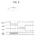
- FIG. 6 is a timing diagram illustrating the operation of the pixel circuit of the OLED device shown in FIG. 4.
- Embodiments will now be described more fully hereinafter with reference to the accompanying drawings, in which exemplary embodiments of the invention are shown.
- FIG. 3 is a schematic diagram of an organic light emitting diode (OLED) display device according to an exemplary embodiment of the present invention.
- Referring to FIG. 3, the OLED device according to the embodiment of the of FIG. 3 includes a
pixel portion 100, ascan driver 200, anemission driver 300, adata driver 400, ademultiplexer unit 500, adata line selector 600, and atiming controller 700. - The
scan driver 200 sequentially supplies scan signals to a plurality of scan lines S1-S2n synchronously with scan control signals Sg (i.e., a start pulse and clock signals) supplied from thetiming controller 700. - The
emission driver 300 may include shift registers, which output emission control signals synchronously with control signals (i.e., the start pulse and clock signals) supplied from thetiming controller 700. Also, the OLED device may not additionally include theemission driver 300. That is, even if the OLED device does not include theemission driver 300, emission control signals can be generated by performing a logic operation on output signals or scan signals of shift registers output from thescan driver 200. - The
data driver 400 receives red (R), green (G), and blue (B) data and control signals Dg (i.e., the start pulse and clock signals) from thetiming controller 700. Thedata driver 400 includes a plurality ofdata driving circuits 450, which supply data signals to data output lines DL1-DLm, respectively, and each of thedata driving circuits 450 receives the R, G, and B data and the control signals Dg from thetiming controller 700. - Each of the
data driving circuits 450 includes a shift register, a sampling latch, a holding latch, and a digital/analog (D/A) converter. The shift register transmits sequentially-supplied data to each sampling latch in bit units in response to the control signal Dg. The sampling latch receives 1-bit data from the shift register and samples the data. The holding latch holds the sampled data, and the D/A converter converts the stored data into an analog value. Also, thedata driving circuit 450 may further include a level shifter, which raises the output signal of the holding latch and supplies the output signal to the D/A converter. - The number of data supplied to each of the
data driving circuits 450 corresponds to the number of data lines D1-Dk connected to onedemultiplexer 550. Accordingly, when each of thedata driving circuits 450 is connected to thedemultiplexer 550, which supplies the data signals to the data lines D1, D2, and D3, it receives three data for one horizontal period. - This
data driving circuit 450 samples the received R, G, and B data, converts the sampled data into an analog data signal, and supplies the data signal to the data output line DLm. - The
demultiplexer unit 500 receives the data signals from the data output lines DL1-DLm and supplies the data signals to the data lines D1-Dmk in response to demultiplexer control signals MC1, MC2, ..., and MCk. Thedemultiplexer unit 500 includes a plurality ofdemultiplexers 550 that are connected to the data output lines DL1-DLm from the respectivedata driving circuits 450 and receive the data signals therefrom. - Each of the
demultiplexers 550 receives the data signal from the data output line DL1-DLm from onedata driving circuit 450 and supplies the data signal to the respective data lines D1, D2, ..., and Dk in response to the control signals MC1, MC2, ..., and MCk supplied from thetiming controller 700. - When each of the
demultiplexers 550 receives three data signals for one horizontal period, it includes three transistors M1, M2, and M3, which are connected to three (k=3) data lines D1, D2, and D3, respectively. - The transistor M1 is turned on in response to the control signal MC1 supplied from the
timing controller 700 and supplies the data signal from the data output line DL1 to the corresponding data line D1. Also, the transistors M2 and M3 perform similar operations as the transistor M1. The operations of the transistors M1, M2, and M3 are sequentially performed, and detailed descriptions thereof will be described later. - The transistors M1, M2, and M3 are p-type metal oxide semiconductor field effect transistors (MOSFETs). Accordingly, the transistors M1, M2, and M3 of the
demultiplexer unit 500 can be produced by the same process as transistors of a pixel circuit formed in thepixel portion 100. Thedemultiplexer unit 500 is formed on the same substrate as thepixel portion 100, thereby realizing a system on panel (SOP) device. Other embodiments may use various other switching devices, such as n-type transistors. - The
pixel portion 100 includes a plurality of pixels P11-P2nmk, which are formed in regions defined by a plurality of scan lines S1-S2n, a plurality of emission control lines E1-E2n, and a plurality of data lines D1-Dmk. Each of the pixels P11-P2nmk includes R, G, and B sub-pixels and receives a data signal from thedata driving circuit 300. - The R, G, and B sub-pixels of the pixel P2nmk each have the same pixel circuit construction. The R, G, and B sub-pixels emit R, G, and B light corresponding to current supplied to an organic light emitting diode. Accordingly, the pixel P2nmk combines the light emitted by the R, G, and B sub-pixels and displays a specific color.
- In the
pixel portion 100, two sub data lines D1a and D1b are formed across respective pixel columns P11-P2n1. The two sub data lines D1a and D1b receive one data signal from thedemultiplexer 550 and selectively supplies the data signal to the pixel columns P11-P2n1. The first sub data line D1a is connected to pixels P11, P31, PS1,..., and P2n-11 of (2n-1)th rows (odd rows) among pixels arranged in the pixel columns P11-P2n1 and supplies the data signals to the respective pixels P11, P31, P51,..., and P2n-11. The second sub data line D1b is connected to pixels P21, P41, ..., and P2n of 2n-th rows (even rows) among the pixels arranged in the pixel columns P11-P2n1 and supplies the data signals to the respective pixels P21, P41, ..., and P2n. - Since the above-described data lines D1a-Dmkb are formed across the
pixel portion 100, they have capacitance. The capacitance caused by the data lines D1a-Dmkb leads to a loading effect when the data signal is applied from thedata driver 400. That is, a delay in transmitting signals occurs due to undesired impedance elements. This capacitance is generated by a parasitic capacitor, which is equivalently induced by conductive layers or metal interconnections opposite insulating layers that are formed on or near the data lines Dmkb and the pixels P1mk-P2nmk. Accordingly, the OLED device having thedemultiplexers 550 needs sufficient time to supply the data signal to the parasitic capacitor of the data line Dmkb. - As described above, the OLED device having the double sub data lines D1a and D1b includes the
data line selector 600, which is disposed between thedemultiplexer unit 500 and thepixel portion 100 and selectively supplies the data signal to the two sub data lines D1a and D1b. - The
data line selector 600 includes two transistors M1a and M1b, which are commonly connected to the transistor M1 of thedemultiplexer 550 and respectively connected to the two sub data lines D1a and D1b of the pixel columns P11-P2n1 that receive the data signal from the transistor M1 of thedemultiplexer 550. - The first transistor M1a, which is connected to the first sub data line D1a, is turned on in response to a control signal DCa output from the
timing controller 700 and transmits the data signal from the transistor M1 of thedemultiplexer 550 to the first sub data line D1a. - The second transistor M1b, which is connected to the second sub data line D1b, is turned on in response to a control signal DCb output from the
timing controller 700 and transmits the data signal from the transistor M1 of thedemultiplexer 550 to the second sub data line D1b. - The first and second transistors M1a and M1b are alternately turned on and off, and the first and second sub data lines D1a and D1b selectively receive the data signal.
- The above-described first and second transistors M1a and M1b of the
data line selector 600 are p-type MOSFETs. Thus, the transistors M1a and M1b of thedata line selector 600 can be produced by the same process as the transistors of thepixel portion 100. Thedata line selector 600 and thepixel portion 100 are formed on one substrate at the same time, thereby realizing the SOP type. In some embodiments, the first and second transistors M1a and M1b are other types of switches, such as n-type transistors. - The operation of the OLED device shown in FIG. 3 will now be described with reference to FIG. 4.
- FIG. 4 is a timing diagram illustrating the operation of the OLED device shown in FIG. 3.
- Hereinafter, the
first demultiplexer 550 receiving data signals from the firstdata driving circuit 450 and the k pixels P11-P1k receiving the data signals from thefirst demultiplexer 550 will be described. Also, it will be assumed that onedemultiplexer 550 supplies the data signal to three pixel columns P11-P1k (k=3) and includes three transistors M1, M2, and M3. - When the
scan driver 200 supplies a low-level first scan signal, a first-row first-column pixel (P11) data signal stored in the first sub data line D1a of a first column is transmitted to an enabled first-row first-column pixel P11. Also, a first-row second column pixel (P12) data signal stored in a first sub data line D2a of a second column is transmitted to an enabled first-row second-column pixel P12, and a first-row third-column pixel (P13) data signal stored in a first sub data line D3a of a third column is transmitted to a first-row third-column pixel P13. - During the supply of the low-level first scan signal, three second transistors M1b, M2b, and M3b of the
data line selector 600, which are connected to second sub data lines D1b-D3b of the first through third columns, respectively, receive a low-level control signal DCb from thetiming controller 700 and, in response, turn on. - While the second transistors M1b, M2b, and M3b of the
data line selector 600 are on, the firstdata driving circuit 450 transmits a second-row first-column pixel (P21) data signal through the data output line DL1 to thedemultiplexer 550. The transistor M1 of thedemultiplexer 550, which is connected to the data line D1 of the pixels P11-P2n1 of the first row, is turned on in response to the control signal MC1 output from thetiming controller 700 and outputs the second-row first-column pixel (P21) data signal. The second-row first-column pixel (P21) data signal is supplied through the turned-on second transistor M1b of thedata line selector 600 to the second sub data line D1b. - Next, when the first
data driving circuit 450 transmits a second-row second-column pixel P22 data signal through the data output line DL1 to thedemultiplexer 550, the transistor M2 of thedemultiplexer 550, which is connected to the data line D2 of pixels P12-P2n2 of the second row, receives the control signal MC2 from thetiming controller 700 and then is turned on. Accordingly, a second sub data line D2b of the pixels P12-P2n2 of the second row receives a second-row second-column pixel (P22) data signal through the transistor M2 of thedemultiplexer 550 and the second transistor M2b of thedata line selector 600. - Finally, when the first
data driving circuit 450 transmits a second-row third-column pixel (P23) data signal through the data output line DL1 to thedemultiplexer 550, the transistor M3 of thedemultiplexer 550, which is connected to the data line D3 of pixels P13-P2n3 of the third column, receives the control signal MC3 from thetiming controller 700 and turns on. Accordingly, the second sub data line D2b of the pixels P13-P2n3 of the third column receives a second-row third-column pixel (P23) data signal through the transistor M3 of thedemultiplexer 550 and the second transistor M3b of thedata line selector 600. - As described above, during the supply of the low-level first scan signal, the second transistors M1b, M2b, and M3b of the
data line selector 600 are turned on, and each of thedemultiplexers 550 sequentially turns on a transistors M1-Mk. Accordingly, the data signals of the pixels P21-P2k of the second row are supplied to the second sub data lines D1b-Dkb through the turned-on second transistors M1b, M2b, and M3b, respectively. - As explained above, the operation of sequentially supplying data signals of k pixels P11-P1k is performed by an m number of
data driving circuits 450 at the same time. Also, the operation of outputting the data signals by sequentially turning on k transistors M1-Mk is performed by an m number ofdemultiplexers 550 at the same time. Accordingly, transistors M1, Mk+1, ..., M(m-1)k+ 1, which operate symmetrically in the m number ofdemultiplexers 550, receive the same control signal MC1 from thetiming controller 700 and turn on at the same time. The operation of turning on the second transistor M1b of thedata line selector 600 during the supply of the first scan signal is performed in an m x k number of second transistors M1b, M2b, M3b,... at the same time. Accordingly, the m x k second transistors M1b, M2b, M3b,..., which operate symmetrically, receive the same control signal DCb from thetiming controller 700 and turn on at the same time. The control signal DCb is active for the same amount of time as the scan signal and remains at a low level while the low-level first scan signal is being supplied. Therefore, the control signal DCb can be obtained by performing a logic operation on output signals of thescan driver 200. - Once the
scan driver 200 supplies a low-level second scan signal to thepixel portion 100, the pixels P21-P2k of the second row are enabled. Thus, the second-row first-column (P21) data signal, which is stored in the second sub data line D1b of a first column, is transmitted to the enabled second-row first-column pixel P21. Also, the second-row second-column (P22) data signal, which is stored in the second sub data line D2b of a second column, is transmitted to the enabled second-row second-column pixel P22, and the second-row third-column (P23) data signal, which is stored in the second sub data line D3b of a third column, is transmitted to the enabled second-row third-column pixel P23. - Accordingly, a sufficient electric charge is shared between a parasitic capacitor of each sub data line and a storage capacitor of each pixel for a scan period having an active duration of one horizontal period, so that the storage capacitor of the pixel is charged with an electric charge corresponding to the data signal.
- During the supply of the low-level second scan signal, the first transistors M1a, M2a, and M3a of the three
data line selector 600, which are connected to the first sub data lines D1a-D3a of the first through third columns, respectively, receive a low-level control signal DCa from thetiming controller 700 and then turn on at the same time. - While the first transistors M1a, M2a, and M3a of the
data line selector 600 are turned on, the firstdata driving circuit 450 sequentially generates a third-row first-column pixel (P31) data signal, a third-row second-column pixel (P32) data signal, and a third-row third-column pixel (P33) data signal. The three data signals are transmitted to thedata line selector 600 through the three transistors M1, M2, and M3, which are sequentially turned on in response to the control signals MC1, MC2, and MC3 of thetiming controller 700. Also, the three data signals are supplied to the three first sub data lines D1a, D2a, and D3a, respectively, through the turned-on first transistors M1a, M2a, and M3a of thedata line selector 600. - As described above, during the supply of the low-level second scan signal, the k first transistors M1a, M2a, M3a, ... of the
data line selector 600 are turned on, and each of thedemultiplexers 550 sequentially turns on the transistors M1-Mk. Thus, data signals of pixels P31-P3k of the third row are supplied to the first sub data lines D1a, D2a, and D3a, respectively, through the turned-on transistors M1a, M2a, M3a,... - As explained above, the operation of sequentially supplying the data signals of the k pixels P11-P1k is performed by the m
data driving circuits 450. Also, the operation of outputting the data signals by sequentially turning on the k transistors M1-Mk is performed by them demultiplexers 550. Accordingly, the transistors M1, Mk+1, ..., M(m-1)k+ 1, which operate symmetrically in them demultiplexers 550, receive the same control signal MC1 from thetiming controller 700 and turn on at the same time. The operation of turning on the first transistor M1a of thedata line selector 600 during the supply of the first scan signal is performed in the m x k first transistors M1a, M2a, M3a,... at the same time. Accordingly, the m x k first transistors M1a, M2a, M3a,..., which operate symmetrically, receive the same control signal DCa from thetiming controller 700 and turn on at the same time. The control signal DCa has the same amount of active time as the scan signal and remains at a low level during the supply of the low-level second scan signal. Therefore, the control signal DCa can be obtained by performing a logic operation on output signals of thescan driver 200. - The above-described operations are repeatedly continued until a 2n-th scan signal is supplied and an electric charge is shared by pixels P2n1-P2nmk arranged in a 2n-th row.
- Therefore, when a low-level (2n-1)th (n is an odd number) scan signal is supplied, the second transistor M1b of the
data line selector 600 turns on and supplies a 2n-row pixel (P2n1) data signal to the second sub data line D1b. Also, when a low-level 2n-th (n is an even number) scan signal is supplied, the first transistor M1a of thedata line selector 600 turns on and supplies a (2n+1)-row pixel (P2n+11) data signal to the first sub data line D1a. - In the above-described operations, a data signal is supplied to a data line for the previous scan period and an electric charge is shared between an enabled pixel and the data line for the present scan period. Thus, sufficient time to supply the data signal and share the electric charge can be ensured.
- FIG. 5 is a circuit diagram of two pixels of the OLED device shown in FIG. 3.
- For brevity of explanation, only a pixel P2nmk that receives a 2n-th scan signal and a 2n-th emission control signal and also receives a data signal from an mk-th data line will be described with reference to FIG. 5.
- Referring to FIG. 5, the pixel P2nmk of the OLED device includes transistors M21, M22, and M23, a storage capacitor Cst2, and an organic light emitting diode OLED2.
- The driving transistor M21 is a transistor for controlling a driving current supplied to the organic light emitting diode OLED2. The driving transistor M21 has a source electrode connected to a power supply voltage VDD, and a drain electrode connected to a source electrode of the emission control transistor M23.
- The emission control transistor M23 is a transistor for enabling or blocking the flow of current into the organic light emitting diode OLED2. The emission control transistor M23 has the source electrode connected to the drain electrode of the driving transistor M21, and a drain electrode connected to an anode electrode of the organic light emitting diode OLED2.
- The organic light emitting diode OLED2 has a cathode electrode connected to a power supply voltage VSS, and the anode electrode connected to the drain electrode of the emission control transistor M23. The organic light emitting diode OLED2 emits light corresponding to the amount of driving current supplied from the driving transistor M21.
- The switching transistor M22 transmits a data signal Vdata applied to the second sub data line Dmkb to one electrode of the storage capacitor Cst2 in response to a scan signal applied from the scan line S2n.
- The storage capacitor Cst2 has one electrode connected to a gate electrode of the driving transistor M21, and the other electrode connected to the power supply voltage VDD.
- Hereinafter, the operations of the pixel circuit shown in FIG. 5 will be described with reference to FIG. 6.
- FIG. 6 is a timing diagram illustrating the operation of the pixel circuit of the OLED device shown in FIG. 4.
- Once the
scan driver 200 supplies a low-level (2n-1)th scan signal, the second transistor Mmkb of thedata line selector 600 turns on and supplies a 2n-row mk-column pixel (P2nmk) data signal to the second sub data line Dmkb. The second sub data line Dmkb has a capacitor Cdata2, which is formed between the second sub data line Dmkb and nearby metal interconnections Accordingly, the capacitor Cdata2 in the second sub data line Dmkb is charged with an electric charge corresponding to the 2n-row mk-column pixel (P2nmk) data signal. However, since the switching transistor M22 of the pixel P2nmk is turned off, no electric charge is shared between the storage capacitor Cst2 of the pixel P2nmk and the capacitor Cdata2 in the second sub data line Dmkb. - Next, once the
scan driver 200 supplies a low-level 2n-th scan signal, the pixel P2nmk is enabled. Thus, the switching transistor M22 is turned on, so that the storage capacitor Cst2 of the pixel P2nmk and the capacitor Cdata2 in the second sub data line Dmkb are connected to each other by the switching transistor M22 and have an electric charge in common. Thus, the storage capacitor Cst2 is charged with an electric charge corresponding to a difference between the power supply voltage VDD and the data voltage Vdata. Subsequently, once a low-level emission control signal is applied to the emission control transistor M23, the emission control transistor M23 is turned on, and thus the driving transistor M21 is connected to the organic light emitting diode OLED2. Accordingly, current corresponding to the electric charge stored in the storage capacitor Cst2 flows from the drain electrode of the driving transistor M21 to the anode electrode of the organic light emitting diode OLED2, so that the organic light emitting diode OLED2 emits light. - As described above, a data signal is supplied and an electric charge is shared between the capacitor Cdata2 of the data line and the storage capacitor Cst2 of the pixel P2nmk for a sufficient time that the organic light emitting diode display device can emit light with a luminance corresponding to the data signal. Although it is described that the pixel circuit includes only the three transistors M21, M22, and M23 and one capacitor Cst2, the present invention is not limited thereto, but other embodiments of the pixel circuit can be used.
- As described above, the OLED device having demultiplexers includes two data lines in each pixel column. Thus, a data signal is supplied for the previous scan period and transmitted to a corresponding pixel for the present scan period. As a result, time taken to supply and transmit the data signal is sufficient, so that the OLED device can emit light with a luminance corresponding to the supplied data signal.
- Although certain embodiments have been described, it will be understood by those skilled in the art that a variety of modifications and variations may be made without departing from the scope of the present invention.
Claims (20)
- An organic light emitting diode (OLED) display device comprising:an array of pixels, the array arranged in rows and columns;a plurality of scan lines connected to rows of pixels;a plurality of data lines, each data line being connected to one or more pixels of a column and each data line being not connected to one or more other pixels of the column; anda data driver for supplying data signals for the data lines.
- An OLED device according to claim 1, further comprising a demultiplexer configured to receive the data signals from the data driver and to supply the data signals to at least two of the data lines.
- An OLED device according to claim 1 or 2, further comprising a scan driver configured to sequentially supply a scan signal to each of the rows, wherein the data driver is configured to supply the data signal to a data line connected to a pixel of a next row during a time when the scan driver supplies a scan signal to a current row.
- An OLED device according to claim 3, wherein the data line connected to the pixel of the next row is configured to store the data signal during the time when the scan driver supplies the scan signal to the current row, and to provide the data signal to the pixel of the next row during a time when the scan driver supplies a scan signal to the next row.
- An OLED device according to claim 4, wherein the pixel of the next row is configured to store the data signal, and to provide a current to a light emitting diode, the current being generated based on the data signal.
- An OLED device according to any one of claims 1 to 5, wherein each data line is connected to pixels of a single column, wherein the pixels of the single column are either of even number rows or of odd number rows.
- An OLED device according to any one of claims 2 to 6, wherein the demultiplexer and the array are formed on the same substrate.
- An organic light emitting diode (OLED) display device according to any one of Claims 1 to 7 wherein the array of pixels form at least part of a pixel portion for displaying an image, the OLED device further comprising:a scan driver for supplying a scan signal to the pixel portion;an emission driver for supplying an emission control signal to the pixel portion; anda demultiplexer for receiving the data signal from the data driver and for supplying the data signal to at least two columns of the pixel portion,and wherein the pixel portion is configured to receive the data signal from the demultiplexer and to supply alternately the data signal through at least two data lines to pixels arranged in a single column.
- An OLED device according to claim 8, wherein the demultiplexer includes at least two transistors, which are configured to be sequentially turned on and to supply the data signal to the at least two columns of the pixel portion.
- An OLED device according to claim 8 or 9, further comprising :a plurality of emission control lines for transmitting the emission control signal to pixels arranged in the rows; wherein the plurality of data lines comprises:a plurality of first data lines disposed on one side of pixels arranged in the columns; anda plurality of second data lines disposed on the other side of the pixels arranged in the columns.
- An OLED device according to claim 10, wherein the first data lines are configured to transmit the data signal to pixels arranged in odd rows, and the second data lines are configured to transmit the data signals to the pixels arranged in even rows.
- An OLED device according to claim 10 or 11, further comprising first and second transistors disposed between the demultiplexer and the first and second data lines, the first and second transistors configured to receive the data signal from the demultiplexer and to alternately supply the data signal to the first and second data lines.
- An OLED device according to claim 12, wherein the first transistors are connected to the first data lines and are configured to be turned on when the scan driver supplies the scan signal to the pixels arranged in the even rows, and to supply the data signal to the first data lines, and the second transistors are connected to the second data lines and are configured to be turned on when the scan driver supplies the scan signal to the pixels arranged in the odd rows, and to supply the data signal to the second data lines.
- An OLED device according to claim 13, wherein the transistors of the demultiplexer and the first and second transistors connected to the first and second data lines are PMOS transistors.
- An OLED device according to any one of claims 12 to 14, wherein the demultiplexer, the first and second transistors connected to the first and second data lines, and the pixel portion are formed on the same substrate.
- A method of operating an OLED device having a demultiplexer, the method comprising:during a previous scan period, supplying a data signal from the demultiplexer either to a first data line connected to pixels arranged in odd rows, or to a second data line connected to pixels arranged in even rows; andduring a current scan period, transmitting the supplied data signal from the first or second data line to a pixel.
- The method according to claim 16, wherein supplying the data signal comprises sequentially outputting data signals for at least two pixels by sequentially turning on at least two transistors of the demultiplexer.
- The method according to claim 17, wherein supplying the data signal from the demultiplexer either to the first data line or to the second data line comprises either selectively turning on a first transistor disposed between the demultiplexer and the first data line or a second transistor disposed between the demultiplexer and the second data line.
- A method according to claim 18, wherein supplying the data signal from the demultiplexer either to the first data line or to the second data line further comprises turning on a transistor of a pixel so as to transmit the data signal to the pixel.
- A method according to claim 19, wherein the transistors of the demultiplexer and the first and second transistors connected to the first and second data lines are PMOS transistors.
Applications Claiming Priority (1)
| Application Number | Priority Date | Filing Date | Title |
|---|---|---|---|
| KR1020050086440A KR100666646B1 (en) | 2005-09-15 | 2005-09-15 | Driving method of organic light emitting display device and organic light emitting display device |
Publications (3)
| Publication Number | Publication Date |
|---|---|
| EP1764772A2 true EP1764772A2 (en) | 2007-03-21 |
| EP1764772A3 EP1764772A3 (en) | 2007-11-21 |
| EP1764772B1 EP1764772B1 (en) | 2014-02-26 |
Family
ID=37440951
Family Applications (1)
| Application Number | Title | Priority Date | Filing Date |
|---|---|---|---|
| EP06254812.8A Active EP1764772B1 (en) | 2005-09-15 | 2006-09-15 | Organic light emitting diode display device and method of operating the same |
Country Status (4)
| Country | Link |
|---|---|
| US (1) | US8730132B2 (en) |
| EP (1) | EP1764772B1 (en) |
| KR (1) | KR100666646B1 (en) |
| CN (1) | CN100547637C (en) |
Cited By (4)
| Publication number | Priority date | Publication date | Assignee | Title |
|---|---|---|---|---|
| US20110227885A1 (en) * | 2010-03-16 | 2011-09-22 | Bo-Yong Chung | Pixel and Organic Light Emitting Display Device Using the Same |
| US20120313903A1 (en) * | 2011-06-10 | 2012-12-13 | Samsung Mobile Display Co., Ltd. | Organic light emitting display |
| EP3300066A1 (en) * | 2016-09-22 | 2018-03-28 | LG Display Co., Ltd. | Organic light emitting display device |
| JP2025119569A (en) * | 2024-02-01 | 2025-08-14 | エルジー ディスプレイ カンパニー リミテッド | display device |
Families Citing this family (69)
| Publication number | Priority date | Publication date | Assignee | Title |
|---|---|---|---|---|
| KR100873705B1 (en) | 2007-06-22 | 2008-12-12 | 삼성모바일디스플레이주식회사 | Organic light emitting display device and manufacturing method |
| KR100911982B1 (en) * | 2008-03-04 | 2009-08-13 | 삼성모바일디스플레이주식회사 | Emission driver and organic light emitting display device using same |
| JP2009211039A (en) * | 2008-03-04 | 2009-09-17 | Samsung Mobile Display Co Ltd | Organic light emitting display device |
| KR100924143B1 (en) | 2008-04-02 | 2009-10-28 | 삼성모바일디스플레이주식회사 | Flat Panel Display and Driving Method |
| KR101064466B1 (en) * | 2009-07-29 | 2011-09-16 | 삼성모바일디스플레이주식회사 | Organic light emitting display |
| JP6141590B2 (en) * | 2011-10-18 | 2017-06-07 | セイコーエプソン株式会社 | Electro-optical device and electronic apparatus |
| KR101873723B1 (en) * | 2012-02-02 | 2018-07-04 | 삼성디스플레이 주식회사 | Organic electro luminescence display device |
| JP2013231920A (en) * | 2012-05-01 | 2013-11-14 | Samsung R&D Institute Japan Co Ltd | Electro-optic device and drive method for the same |
| KR20140024571A (en) | 2012-08-20 | 2014-03-03 | 삼성디스플레이 주식회사 | Display device and driving method thereof |
| KR102035718B1 (en) * | 2012-11-26 | 2019-10-24 | 삼성디스플레이 주식회사 | Organic Light Emitting Display Device and Driving Method Thereof |
| KR102022387B1 (en) * | 2012-12-05 | 2019-09-19 | 삼성디스플레이 주식회사 | Organic light emitting diplay and method for operating the same |
| KR102072678B1 (en) * | 2013-07-09 | 2020-02-04 | 삼성디스플레이 주식회사 | Organic light emitting device |
| KR102084231B1 (en) * | 2013-08-29 | 2020-03-04 | 삼성디스플레이 주식회사 | Organic light emitting display device and driving method thereof |
| KR102118096B1 (en) | 2013-12-09 | 2020-06-02 | 엘지디스플레이 주식회사 | Liquid crystal display device |
| TWI522989B (en) * | 2014-01-29 | 2016-02-21 | 友達光電股份有限公司 | Display panel and demultiplexer circuit thereof |
| US20160093260A1 (en) * | 2014-09-29 | 2016-03-31 | Innolux Corporation | Display device and associated method |
| KR102261352B1 (en) * | 2014-12-31 | 2021-06-04 | 엘지디스플레이 주식회사 | Data controling circuit and flat panel display device |
| KR102357345B1 (en) * | 2015-01-27 | 2022-02-03 | 삼성디스플레이 주식회사 | Organic light emitting display device |
| KR102287821B1 (en) * | 2015-02-16 | 2021-08-10 | 삼성디스플레이 주식회사 | Organic light emitting display device and display system having the same |
| KR102356294B1 (en) * | 2015-04-16 | 2022-01-28 | 삼성디스플레이 주식회사 | Display apparatus |
| KR102397991B1 (en) * | 2015-06-24 | 2022-05-13 | 삼성디스플레이 주식회사 | Display device |
| KR102552583B1 (en) * | 2015-07-22 | 2023-07-06 | 삼성디스플레이 주식회사 | Display device |
| KR102482846B1 (en) * | 2015-09-10 | 2023-01-02 | 삼성디스플레이 주식회사 | Display device |
| CN105810173B (en) * | 2016-05-31 | 2018-08-14 | 武汉华星光电技术有限公司 | Multiplexing display driver circuit |
| CN106057164A (en) * | 2016-08-10 | 2016-10-26 | 武汉华星光电技术有限公司 | RGBW four primary color panel driving framework |
| CN106531096B (en) * | 2016-11-28 | 2019-12-24 | 武汉华星光电技术有限公司 | RGBW four primary color display panel driving method |
| TWI612367B (en) * | 2017-01-04 | 2018-01-21 | 友達光電股份有限公司 | Pixel array structure |
| KR102839232B1 (en) | 2017-01-04 | 2025-07-30 | 삼성디스플레이 주식회사 | Display device |
| KR102794297B1 (en) | 2017-02-01 | 2025-04-15 | 삼성디스플레이 주식회사 | Display device |
| KR20250024112A (en) * | 2017-02-17 | 2025-02-18 | 가부시키가이샤 한도오따이 에네루기 켄큐쇼 | Display device |
| CN106935217B (en) | 2017-03-23 | 2019-03-15 | 武汉华星光电技术有限公司 | Multiple-channel output selection circuit and display device |
| TWI638345B (en) * | 2017-07-03 | 2018-10-11 | 友達光電股份有限公司 | Display and associated data dispatching circuit |
| US10255864B2 (en) * | 2017-07-24 | 2019-04-09 | Wuhan China Star Optoelectronics Technology Co., Ltd. | Demux control circuit |
| US10789873B2 (en) * | 2017-08-23 | 2020-09-29 | HKC Corporation Limited | Driving device and driving method of display device |
| US11211020B2 (en) * | 2017-09-21 | 2021-12-28 | Apple Inc. | High frame rate display |
| US11741904B2 (en) * | 2017-09-21 | 2023-08-29 | Apple Inc. | High frame rate display |
| WO2019060105A1 (en) | 2017-09-21 | 2019-03-28 | Apple Inc. | High frame rate display |
| KR102383564B1 (en) * | 2017-10-23 | 2022-04-06 | 엘지디스플레이 주식회사 | Display panel and electroluminescence display using the same |
| KR102487500B1 (en) * | 2018-01-02 | 2023-01-12 | 삼성디스플레이 주식회사 | Display device |
| US11250787B2 (en) | 2018-02-02 | 2022-02-15 | Chengdu Boe Optoelectronics Technology Co., Ltd. | Signal control apparatus and method, display control apparatus and method, and display apparatus |
| CN109427292B (en) | 2018-02-02 | 2021-04-02 | 京东方科技集团股份有限公司 | A signal control device and method, a display control device and method, and a display device |
| CN109785789B (en) * | 2018-04-18 | 2021-11-16 | 友达光电股份有限公司 | Multiplexer and display panel |
| CN208521584U (en) * | 2018-07-24 | 2019-02-19 | 京东方科技集团股份有限公司 | A pixel structure, display panel and display device |
| KR102482983B1 (en) | 2018-08-02 | 2022-12-30 | 삼성디스플레이 주식회사 | Display panel and display device |
| KR20200017614A (en) * | 2018-08-08 | 2020-02-19 | 삼성디스플레이 주식회사 | Display device |
| CN110827765B (en) | 2018-08-08 | 2021-04-09 | 京东方科技集团股份有限公司 | Display panel and driving method thereof, and display device |
| KR102794230B1 (en) * | 2018-12-07 | 2025-04-14 | 삼성디스플레이 주식회사 | Display device and driving method thereof |
| TWI696165B (en) * | 2019-01-16 | 2020-06-11 | 友達光電股份有限公司 | Display device and multiplexer thereof |
| CN109697967A (en) * | 2019-03-08 | 2019-04-30 | 京东方科技集团股份有限公司 | A kind of dot structure and its driving method, display device |
| CN110335561B (en) * | 2019-04-03 | 2021-03-16 | 武汉华星光电技术有限公司 | Multiplexing circuit |
| CN110808005A (en) * | 2019-04-25 | 2020-02-18 | 华为技术有限公司 | Display screen, mobile terminal and control method thereof |
| KR102717975B1 (en) * | 2019-05-14 | 2024-10-17 | 삼성디스플레이 주식회사 | Display device and method of driving the same |
| KR102582836B1 (en) * | 2019-06-07 | 2023-09-27 | 삼성디스플레이 주식회사 | Touch panel and a display divice including the same |
| CN112837657A (en) * | 2019-11-22 | 2021-05-25 | 敦泰电子股份有限公司 | Driving method for improving refresh rate of display device and display device using the same |
| CN115762387B (en) * | 2019-12-27 | 2025-01-07 | 厦门天马微电子有限公司 | Display panel, driving method thereof and display device |
| CN113096596B (en) * | 2020-01-08 | 2025-03-28 | 京东方科技集团股份有限公司 | Display substrate, driving method thereof, and display device |
| CN111383576A (en) * | 2020-03-24 | 2020-07-07 | 维沃移动通信有限公司 | Pixel driving circuit, display panel and electronic equipment |
| CN111292665B (en) | 2020-03-27 | 2022-11-04 | 京东方科技集团股份有限公司 | Pixel circuit and control method thereof, and display device |
| US11282438B2 (en) * | 2020-03-30 | 2022-03-22 | Novatek Microelectronics Corp. | Driver circuit and a display apparatus |
| JP7438044B2 (en) * | 2020-07-10 | 2024-02-26 | シャープ株式会社 | Active matrix substrate and display device equipped with the same |
| CN112071253A (en) | 2020-09-15 | 2020-12-11 | 武汉华星光电半导体显示技术有限公司 | Display panel, driving method thereof and display device |
| CN112863426A (en) * | 2021-01-08 | 2021-05-28 | 武汉华星光电半导体显示技术有限公司 | Display panel and display device |
| CN113035117A (en) * | 2021-03-15 | 2021-06-25 | 京东方科技集团股份有限公司 | Array substrate, driving method thereof and display device |
| CN113299236A (en) * | 2021-05-24 | 2021-08-24 | 京东方科技集团股份有限公司 | Display panel driving method and device and display panel |
| KR20220161903A (en) * | 2021-05-31 | 2022-12-07 | 엘지디스플레이 주식회사 | Display panel, display device including the display panel and personal immersion system using the display device |
| CN116416936A (en) * | 2021-12-29 | 2023-07-11 | 乐金显示有限公司 | Organic light emitting diode display device and driving method thereof |
| US12615933B2 (en) * | 2022-02-25 | 2026-04-28 | Boe Technology Group Co., Ltd. | Pixel circuit and driving method, display panel and driving method, display device |
| CN115588407B (en) * | 2022-09-30 | 2025-04-22 | 合肥维信诺科技有限公司 | Display panel and driving method thereof |
| KR20240100591A (en) * | 2022-12-22 | 2024-07-02 | 삼성디스플레이 주식회사 | Shift register and display apparatus having the same |
Citations (1)
| Publication number | Priority date | Publication date | Assignee | Title |
|---|---|---|---|---|
| US6366026B1 (en) | 1999-03-05 | 2002-04-02 | Sanyo Electric Co., Ltd. | Electroluminescence display apparatus |
Family Cites Families (19)
| Publication number | Priority date | Publication date | Assignee | Title |
|---|---|---|---|---|
| JP3513371B2 (en) | 1996-10-18 | 2004-03-31 | キヤノン株式会社 | Matrix substrate, liquid crystal device and display device using them |
| TW552573B (en) * | 2001-08-21 | 2003-09-11 | Samsung Electronics Co Ltd | Liquid crystal display and driving method thereof |
| KR100649243B1 (en) * | 2002-03-21 | 2006-11-24 | 삼성에스디아이 주식회사 | Organic electroluminescent display and driving method thereof |
| US6993297B2 (en) | 2002-07-12 | 2006-01-31 | Sony Ericsson Mobile Communications Ab | Apparatus and methods for tuning antenna impedance using transmitter and receiver parameters |
| JP2004077567A (en) * | 2002-08-09 | 2004-03-11 | Semiconductor Energy Lab Co Ltd | Display device and driving method therefor |
| US7271784B2 (en) | 2002-12-18 | 2007-09-18 | Semiconductor Energy Laboratory Co., Ltd. | Display device and driving method thereof |
| GB0301623D0 (en) | 2003-01-24 | 2003-02-26 | Koninkl Philips Electronics Nv | Electroluminescent display devices |
| JP3952979B2 (en) * | 2003-03-25 | 2007-08-01 | カシオ計算機株式会社 | Display drive device, display device, and drive control method thereof |
| JP5122131B2 (en) * | 2003-04-25 | 2013-01-16 | 統寶光電股▲ふん▼有限公司 | Method and apparatus for driving an active matrix display panel |
| KR100515318B1 (en) * | 2003-07-30 | 2005-09-15 | 삼성에스디아이 주식회사 | Display and driving method thereof |
| KR100578914B1 (en) | 2003-11-27 | 2006-05-11 | 삼성에스디아이 주식회사 | Display device using demultiplexer |
| KR100589376B1 (en) | 2003-11-27 | 2006-06-14 | 삼성에스디아이 주식회사 | Light emitting display device using demultiplexer |
| KR100578913B1 (en) * | 2003-11-27 | 2006-05-11 | 삼성에스디아이 주식회사 | Display device using demultiplexer and driving method thereof |
| KR100649245B1 (en) * | 2003-11-29 | 2006-11-24 | 삼성에스디아이 주식회사 | Demultiplexing device and display device using same |
| JP2005266346A (en) * | 2004-03-18 | 2005-09-29 | Seiko Epson Corp | Reference voltage generation circuit, data driver, display device and electronic device |
| US7944414B2 (en) | 2004-05-28 | 2011-05-17 | Casio Computer Co., Ltd. | Display drive apparatus in which display pixels in a plurality of specific rows are set in a selected state with periods at least overlapping each other, and gradation current is supplied to the display pixels during the selected state, and display apparatus |
| KR101055203B1 (en) * | 2004-08-19 | 2011-08-08 | 엘지디스플레이 주식회사 | Liquid crystal display |
| US8199079B2 (en) * | 2004-08-25 | 2012-06-12 | Samsung Mobile Display Co., Ltd. | Demultiplexing circuit, light emitting display using the same, and driving method thereof |
| KR100602361B1 (en) * | 2004-09-22 | 2006-07-19 | 삼성에스디아이 주식회사 | Demultiplexer, light emitting display device using same and driving method thereof |
-
2005
- 2005-09-15 KR KR1020050086440A patent/KR100666646B1/en not_active Expired - Fee Related
-
2006
- 2006-08-18 US US11/506,628 patent/US8730132B2/en active Active
- 2006-09-11 CN CNB2006101516516A patent/CN100547637C/en active Active
- 2006-09-15 EP EP06254812.8A patent/EP1764772B1/en active Active
Patent Citations (1)
| Publication number | Priority date | Publication date | Assignee | Title |
|---|---|---|---|---|
| US6366026B1 (en) | 1999-03-05 | 2002-04-02 | Sanyo Electric Co., Ltd. | Electroluminescence display apparatus |
Cited By (7)
| Publication number | Priority date | Publication date | Assignee | Title |
|---|---|---|---|---|
| US20110227885A1 (en) * | 2010-03-16 | 2011-09-22 | Bo-Yong Chung | Pixel and Organic Light Emitting Display Device Using the Same |
| US8912989B2 (en) * | 2010-03-16 | 2014-12-16 | Samsung Display Co., Ltd. | Pixel and organic light emitting display device using the same |
| US20120313903A1 (en) * | 2011-06-10 | 2012-12-13 | Samsung Mobile Display Co., Ltd. | Organic light emitting display |
| US8816998B2 (en) * | 2011-06-10 | 2014-08-26 | Samsung Display Co., Ltd. | Organic light emitting display |
| EP3300066A1 (en) * | 2016-09-22 | 2018-03-28 | LG Display Co., Ltd. | Organic light emitting display device |
| US10541286B2 (en) | 2016-09-22 | 2020-01-21 | Lg Display Co., Ltd. | Organic light emitting display device |
| JP2025119569A (en) * | 2024-02-01 | 2025-08-14 | エルジー ディスプレイ カンパニー リミテッド | display device |
Also Published As
| Publication number | Publication date |
|---|---|
| EP1764772A3 (en) | 2007-11-21 |
| US20070057877A1 (en) | 2007-03-15 |
| CN1932939A (en) | 2007-03-21 |
| CN100547637C (en) | 2009-10-07 |
| EP1764772B1 (en) | 2014-02-26 |
| KR100666646B1 (en) | 2007-01-09 |
| US8730132B2 (en) | 2014-05-20 |
Similar Documents
| Publication | Publication Date | Title |
|---|---|---|
| EP1764772B1 (en) | Organic light emitting diode display device and method of operating the same | |
| US7808463B2 (en) | Data driver and organic light emitting display having the same | |
| US9177502B2 (en) | Bi-directional scan driver and display device using the same | |
| KR101761794B1 (en) | Display device and driving method thereof | |
| CN101256735B (en) | Organic light emitting display and driving circuit thereof | |
| US8130183B2 (en) | Scan driver and scan signal driving method and organic light emitting display using the same | |
| CN100474373C (en) | Display device and driving method thereof | |
| JP2005049838A (en) | Display device and driving method thereof | |
| CN101256736A (en) | Organic light-emitting display and its driving circuit | |
| WO2019053834A1 (en) | Display device and drive method therefor | |
| JP2006119639A (en) | Light emitting display device and driving method thereof | |
| US9047821B2 (en) | Scan driver and display device using the same | |
| US7486261B2 (en) | Electro-luminescent display device | |
| CN112735332B (en) | Display Devices | |
| KR100649249B1 (en) | Demultiplexing device, light emitting display device and display panel using same | |
| KR20040021753A (en) | Organic electro-luminescent DISPLAY apparatus and driving method thereof | |
| KR100666643B1 (en) | Driving method of organic light emitting display device and organic light emitting display device | |
| US20060221016A1 (en) | Display | |
| US20100085388A1 (en) | Active matrix display device | |
| KR100624134B1 (en) | Driving method of organic light emitting display device | |
| US20260080837A1 (en) | Display Device | |
| US20260120651A1 (en) | Data driver and display device including the same | |
| KR100666647B1 (en) | Driving method of organic light emitting display device and organic light emitting display device | |
| US7696976B2 (en) | Data driver and organic light emitting display device having the same | |
| KR100612280B1 (en) | Inspection device of display panel |
Legal Events
| Date | Code | Title | Description |
|---|---|---|---|
| PUAI | Public reference made under article 153(3) epc to a published international application that has entered the european phase |
Free format text: ORIGINAL CODE: 0009012 |
|
| 17P | Request for examination filed |
Effective date: 20060922 |
|
| AK | Designated contracting states |
Kind code of ref document: A2 Designated state(s): AT BE BG CH CY CZ DE DK EE ES FI FR GB GR HU IE IS IT LI LT LU LV MC NL PL PT RO SE SI SK TR |
|
| AX | Request for extension of the european patent |
Extension state: AL BA HR MK YU |
|
| PUAL | Search report despatched |
Free format text: ORIGINAL CODE: 0009013 |
|
| AK | Designated contracting states |
Kind code of ref document: A3 Designated state(s): AT BE BG CH CY CZ DE DK EE ES FI FR GB GR HU IE IS IT LI LT LU LV MC NL PL PT RO SE SI SK TR |
|
| AX | Request for extension of the european patent |
Extension state: AL BA HR MK YU |
|
| AKX | Designation fees paid |
Designated state(s): DE FR GB |
|
| RAP1 | Party data changed (applicant data changed or rights of an application transferred) |
Owner name: SAMSUNG MOBILE DISPLAY CO., LTD. |
|
| 17Q | First examination report despatched |
Effective date: 20100713 |
|
| RAP1 | Party data changed (applicant data changed or rights of an application transferred) |
Owner name: SAMSUNG DISPLAY CO., LTD. |
|
| GRAP | Despatch of communication of intention to grant a patent |
Free format text: ORIGINAL CODE: EPIDOSNIGR1 |
|
| INTG | Intention to grant announced |
Effective date: 20130830 |
|
| GRAS | Grant fee paid |
Free format text: ORIGINAL CODE: EPIDOSNIGR3 |
|
| GRAA | (expected) grant |
Free format text: ORIGINAL CODE: 0009210 |
|
| AK | Designated contracting states |
Kind code of ref document: B1 Designated state(s): DE FR GB |
|
| REG | Reference to a national code |
Ref country code: GB Ref legal event code: FG4D |
|
| REG | Reference to a national code |
Ref country code: DE Ref legal event code: R096 Ref document number: 602006040374 Country of ref document: DE Effective date: 20140410 |
|
| REG | Reference to a national code |
Ref country code: DE Ref legal event code: R097 Ref document number: 602006040374 Country of ref document: DE |
|
| PLBE | No opposition filed within time limit |
Free format text: ORIGINAL CODE: 0009261 |
|
| STAA | Information on the status of an ep patent application or granted ep patent |
Free format text: STATUS: NO OPPOSITION FILED WITHIN TIME LIMIT |
|
| 26N | No opposition filed |
Effective date: 20141127 |
|
| REG | Reference to a national code |
Ref country code: DE Ref legal event code: R097 Ref document number: 602006040374 Country of ref document: DE Effective date: 20141127 |
|
| REG | Reference to a national code |
Ref country code: FR Ref legal event code: PLFP Year of fee payment: 11 |
|
| REG | Reference to a national code |
Ref country code: FR Ref legal event code: PLFP Year of fee payment: 12 |
|
| REG | Reference to a national code |
Ref country code: FR Ref legal event code: PLFP Year of fee payment: 13 |
|
| P01 | Opt-out of the competence of the unified patent court (upc) registered |
Effective date: 20230515 |
|
| PGFP | Annual fee paid to national office [announced via postgrant information from national office to epo] |
Ref country code: DE Payment date: 20240822 Year of fee payment: 19 |
|
| PGFP | Annual fee paid to national office [announced via postgrant information from national office to epo] |
Ref country code: GB Payment date: 20240822 Year of fee payment: 19 |
|
| PGFP | Annual fee paid to national office [announced via postgrant information from national office to epo] |
Ref country code: FR Payment date: 20240827 Year of fee payment: 19 |