EP1764769A1 - Organic electroluminescent device and driving method thereof - Google Patents
Organic electroluminescent device and driving method thereof Download PDFInfo
- Publication number
- EP1764769A1 EP1764769A1 EP20060010501 EP06010501A EP1764769A1 EP 1764769 A1 EP1764769 A1 EP 1764769A1 EP 20060010501 EP20060010501 EP 20060010501 EP 06010501 A EP06010501 A EP 06010501A EP 1764769 A1 EP1764769 A1 EP 1764769A1
- Authority
- EP
- European Patent Office
- Prior art keywords
- data
- display data
- discharging
- gray scale
- circuit
- Prior art date
- Legal status (The legal status is an assumption and is not a legal conclusion. Google has not performed a legal analysis and makes no representation as to the accuracy of the status listed.)
- Granted
Links
Images



Classifications
-
- G—PHYSICS
- G09—EDUCATION; CRYPTOGRAPHY; DISPLAY; ADVERTISING; SEALS
- G09G—ARRANGEMENTS OR CIRCUITS FOR CONTROL OF INDICATING DEVICES USING STATIC MEANS TO PRESENT VARIABLE INFORMATION
- G09G3/00—Control arrangements or circuits, of interest only in connection with visual indicators other than cathode-ray tubes
- G09G3/20—Control arrangements or circuits, of interest only in connection with visual indicators other than cathode-ray tubes for presentation of an assembly of a number of characters, e.g. a page, by composing the assembly by combination of individual elements arranged in a matrix no fixed position being assigned to or needed to be assigned to the individual characters or partial characters
- G09G3/22—Control arrangements or circuits, of interest only in connection with visual indicators other than cathode-ray tubes for presentation of an assembly of a number of characters, e.g. a page, by composing the assembly by combination of individual elements arranged in a matrix no fixed position being assigned to or needed to be assigned to the individual characters or partial characters using controlled light sources
- G09G3/30—Control arrangements or circuits, of interest only in connection with visual indicators other than cathode-ray tubes for presentation of an assembly of a number of characters, e.g. a page, by composing the assembly by combination of individual elements arranged in a matrix no fixed position being assigned to or needed to be assigned to the individual characters or partial characters using controlled light sources using electroluminescent panels
- G09G3/32—Control arrangements or circuits, of interest only in connection with visual indicators other than cathode-ray tubes for presentation of an assembly of a number of characters, e.g. a page, by composing the assembly by combination of individual elements arranged in a matrix no fixed position being assigned to or needed to be assigned to the individual characters or partial characters using controlled light sources using electroluminescent panels semiconductive, e.g. using light-emitting diodes [LED]
- G09G3/3208—Control arrangements or circuits, of interest only in connection with visual indicators other than cathode-ray tubes for presentation of an assembly of a number of characters, e.g. a page, by composing the assembly by combination of individual elements arranged in a matrix no fixed position being assigned to or needed to be assigned to the individual characters or partial characters using controlled light sources using electroluminescent panels semiconductive, e.g. using light-emitting diodes [LED] organic, e.g. using organic light-emitting diodes [OLED]
- G09G3/3216—Control arrangements or circuits, of interest only in connection with visual indicators other than cathode-ray tubes for presentation of an assembly of a number of characters, e.g. a page, by composing the assembly by combination of individual elements arranged in a matrix no fixed position being assigned to or needed to be assigned to the individual characters or partial characters using controlled light sources using electroluminescent panels semiconductive, e.g. using light-emitting diodes [LED] organic, e.g. using organic light-emitting diodes [OLED] using a passive matrix
-
- G—PHYSICS
- G09—EDUCATION; CRYPTOGRAPHY; DISPLAY; ADVERTISING; SEALS
- G09G—ARRANGEMENTS OR CIRCUITS FOR CONTROL OF INDICATING DEVICES USING STATIC MEANS TO PRESENT VARIABLE INFORMATION
- G09G2310/00—Command of the display device
- G09G2310/02—Addressing, scanning or driving the display screen or processing steps related thereto
- G09G2310/0243—Details of the generation of driving signals
- G09G2310/0248—Precharge or discharge of column electrodes before or after applying exact column voltages
-
- G—PHYSICS
- G09—EDUCATION; CRYPTOGRAPHY; DISPLAY; ADVERTISING; SEALS
- G09G—ARRANGEMENTS OR CIRCUITS FOR CONTROL OF INDICATING DEVICES USING STATIC MEANS TO PRESENT VARIABLE INFORMATION
- G09G2320/00—Control of display operating conditions
- G09G2320/02—Improving the quality of display appearance
-
- G—PHYSICS
- G09—EDUCATION; CRYPTOGRAPHY; DISPLAY; ADVERTISING; SEALS
- G09G—ARRANGEMENTS OR CIRCUITS FOR CONTROL OF INDICATING DEVICES USING STATIC MEANS TO PRESENT VARIABLE INFORMATION
- G09G2320/00—Control of display operating conditions
- G09G2320/02—Improving the quality of display appearance
- G09G2320/0252—Improving the response speed
-
- G—PHYSICS
- G09—EDUCATION; CRYPTOGRAPHY; DISPLAY; ADVERTISING; SEALS
- G09G—ARRANGEMENTS OR CIRCUITS FOR CONTROL OF INDICATING DEVICES USING STATIC MEANS TO PRESENT VARIABLE INFORMATION
- G09G2340/00—Aspects of display data processing
- G09G2340/16—Determination of a pixel data signal depending on the signal applied in the previous frame
-
- G—PHYSICS
- G09—EDUCATION; CRYPTOGRAPHY; DISPLAY; ADVERTISING; SEALS
- G09G—ARRANGEMENTS OR CIRCUITS FOR CONTROL OF INDICATING DEVICES USING STATIC MEANS TO PRESENT VARIABLE INFORMATION
- G09G3/00—Control arrangements or circuits, of interest only in connection with visual indicators other than cathode-ray tubes
- G09G3/20—Control arrangements or circuits, of interest only in connection with visual indicators other than cathode-ray tubes for presentation of an assembly of a number of characters, e.g. a page, by composing the assembly by combination of individual elements arranged in a matrix no fixed position being assigned to or needed to be assigned to the individual characters or partial characters
- G09G3/2007—Display of intermediate tones
-
- G—PHYSICS
- G09—EDUCATION; CRYPTOGRAPHY; DISPLAY; ADVERTISING; SEALS
- G09G—ARRANGEMENTS OR CIRCUITS FOR CONTROL OF INDICATING DEVICES USING STATIC MEANS TO PRESENT VARIABLE INFORMATION
- G09G3/00—Control arrangements or circuits, of interest only in connection with visual indicators other than cathode-ray tubes
- G09G3/20—Control arrangements or circuits, of interest only in connection with visual indicators other than cathode-ray tubes for presentation of an assembly of a number of characters, e.g. a page, by composing the assembly by combination of individual elements arranged in a matrix no fixed position being assigned to or needed to be assigned to the individual characters or partial characters
- G09G3/22—Control arrangements or circuits, of interest only in connection with visual indicators other than cathode-ray tubes for presentation of an assembly of a number of characters, e.g. a page, by composing the assembly by combination of individual elements arranged in a matrix no fixed position being assigned to or needed to be assigned to the individual characters or partial characters using controlled light sources
- G09G3/30—Control arrangements or circuits, of interest only in connection with visual indicators other than cathode-ray tubes for presentation of an assembly of a number of characters, e.g. a page, by composing the assembly by combination of individual elements arranged in a matrix no fixed position being assigned to or needed to be assigned to the individual characters or partial characters using controlled light sources using electroluminescent panels
- G09G3/32—Control arrangements or circuits, of interest only in connection with visual indicators other than cathode-ray tubes for presentation of an assembly of a number of characters, e.g. a page, by composing the assembly by combination of individual elements arranged in a matrix no fixed position being assigned to or needed to be assigned to the individual characters or partial characters using controlled light sources using electroluminescent panels semiconductive, e.g. using light-emitting diodes [LED]
- G09G3/3208—Control arrangements or circuits, of interest only in connection with visual indicators other than cathode-ray tubes for presentation of an assembly of a number of characters, e.g. a page, by composing the assembly by combination of individual elements arranged in a matrix no fixed position being assigned to or needed to be assigned to the individual characters or partial characters using controlled light sources using electroluminescent panels semiconductive, e.g. using light-emitting diodes [LED] organic, e.g. using organic light-emitting diodes [OLED]
- G09G3/3275—Details of drivers for data electrodes
- G09G3/3283—Details of drivers for data electrodes in which the data driver supplies a variable data current for setting the current through, or the voltage across, the light-emitting elements
Definitions
- the present invention relates to an organic electroluminescent device and a driving method thereof. Particularly, the present invention relates to the organic electroluminescent device capable of changing a discharging level according to gray scale, and a driving method thereof.
- An organic electroluminescent device is a device emitting a light having a predetermined wavelength when a certain voltage is applied thereto.
- FIG. 1 is a view showing an organic electroluminescent device in the art.
- FIG. 2 is a timing diagram showing scan signal and data current provided to pixels of FIG. 1.
- the organic electroluminescent device in the art includes a panel 100, a scan driving circuit 110, a control circuit 120, a data driving circuit 130, a pre-charging circuit 140 and a discharging circuit 150.
- the panel 100 includes a plurality of pixels E11 to E44 formed on an emitting area crossing over data lines D1 to D4 and scan lines S1 to S4.
- the scan driving circuit 110 transmits scan signals to the pixels through the scan lines S1 to S4 in sequence.
- the control circuit 120 receives a display data inputted from outside, for example, RGB data, and transmits a control signal to the scan driving circuit 110, the data driving circuit 130, the pre-charging driving circuit 140, and the discharging circuit 150 according to the display data.
- the pre-charging circuit 140 applies a first pre-charge current according to the first display data provided from the control circuit 120 to the data lines D1 to D4 during a first pre-charge time pcha1 as shown in FIG. 2.
- the first pre-charge current is sufficiently overshooting during the first pre-charge time pcha1 because the first display data is high gray scale (80%).
- the pixels E11 to E44 are emitting a light as the gray scale of 80% from the starting time T2 of a low logic area in the second scan signal SP2.
- the data driving circuit 130 provides a first data current (the gray scale of 80%) according to the first display data transmitted from the control circuit 120 to the pixels E11 to E44 through the data lines D1 to D4.
- the discharging circuit 150 discharges the data lines D1 to D4 to a certain discharge level DL1 according to the first display data transmitted from the control circuit 120 during a second discharge time.
- the discharging circuit 150 is formed with a plurality of Zener diodes ZD1 to ZD4, and so the discharge level is uniformly fixed independently of the emitting gray scale of the pixels E11 to E44.
- the pre-charging circuit 140 applies a second pre-charge current according to the second display data provided from the control circuit 120 to the data lines D1 to D4 during a second pre-charge time pcha2.
- the data driving circuit 130 provides a second data current (the gray scale of 20%) according to the second display data transmitted from the control circuit 120 to the pixels E11 to E44 through the data lines D1 to D4.
- the second pre-charge current is not sufficiently overshooting because the second display data is the low gray scale (20%).
- the pixels E11 to E44 emits as the gray scale of 20% after passing the starting time T3 of the low logic area in a third scan signal SP3, like the A area of FIG. 2
- the pixels E11 to E44 could not emit a light with desired brightness.
- the pixels E11 to E44 could not emit a light with desired brightness, and the consumption power is increased to emit a light with desired brightness.
- One object of the present invention is to provide an organic electroluminescent device which can emit a light with desired brightness independently of gray scale by making the discharging circuit regulate the discharge level according to the gray scale, and a driving method thereof.
- Another object of the present invention is to provide an organic electroluminescent device which can emit the pixels as the brightness corresponding to gray scale by modifying a discharge level according to the gray scale by using a variable resistance, and a driving method thereof.
- the light emitting device comprises a plurality of scan lines in a first direction, a plurality of data lines in a second direction different from the first direction, a panel having a plurality of pixels formed on emitting areas that the data lines and the scan lines cross, a control circuit which generates a control signal according to a first display data and a second display data inputted from outside in sequence, and a discharging circuit which discharges the data lines according to a control signal transmitted from the control circuit to a first discharging level corresponding to the first display data during a first discharging time according to the first display data, and discharges the data lines according to a second discharging level corresponding to the second display data during a second discharging time according to the second display data.
- the light emitting device comprises a plurality of scan lines in a first direction, a plurality of data lines in a second direction different from the first direction, a panel having a plurality of pixels formed on emitting areas that the data lines and the scan lines cross, and a discharging circuit which discharges the data lines according to the a first display data and a second display data inputted from outside in sequence to a first discharging level corresponding to the first display data during a first discharging time according to the first display data, and discharges the data lines according to a second discharging level corresponding to the second display data during a second discharging time according to the second display data.
- the method of driving an electroluminescent device having a plurality of pixels formed on emitting areas crossed by data lines and scan lines comprises detecting a gray scale of a data current according to a display data inputted from outside, and discharging the data lines to a discharging level corresponding to the display data according to the detected gray scale.
- the organic electroluminescent device and driving method thereof according to the present invention can emit the pixels as desired brightness independently of the gray scale by making the discharging circuit regulate the discharge level according to the gray scale.
- the organic electroluminescent device and driving method thereof according to the present invention can emit the pixels as brightness corresponding to the gray scale by changing the discharge level according to the gray scale by using a variable resistance.
- FIG. 1 is a view showing an organic electroluminescent device in the art
- FIG. 2 is a timing diagram showing scan signal and data current provided to pixels of FIG. 1;
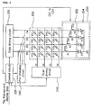
- FIG. 3 is a view schematically showing the organic electroluminescent device according to the first embodiment of the present invention.
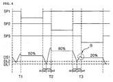
- FIG. 4 is a timing diagram showing scan signal and data current provided to pixels of the organic electroluminescent device according to embodiments of the present invention.
- FIG. 5 is a flow diagram showing the driving method of the organic electroluminescent device according to a first embodiment of the present invention
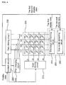
- FIG. 6 is a view schematically showing the organic electroluminescent device according to a second embodiment of the present invention.
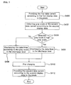
- FIG. 7 is a flow diagram showing the driving method of the organic electroluminescent device according to the second embodiment of the present invention.
- FIG. 3 is a view schematically showing the organic electroluminescent device according to the first embodiment of the present invention.
- FIG. 4 is a timing diagram showing scan signal and data current provided to pixels of the organic electroluminescent device according to embodiments of the present invention.
- the organic electroluminescent device includes a panel 200, a scan driving circuit 210, a control circuit 220, a data driving circuit 230, a pre-charging circuit 240 and a first discharging circuit 250.
- the panel 200 includes a plurality of pixels E11 to E44 formed on an emitting area crossing over data lines D1 to D4 and scan lines S1 to S4.
- Each of the pixels E11 to E44 is formed with an anode electrode layer, an organic layer and a cathode electrode layer, and emits a light having a certain wavelength when a positive voltage is applied to the anode electrode layer and a negative voltage is applied to the cathode electrode layer.
- the scan driving circuit 210 provides scan signals to scan lines S1 to S4 in sequence.
- the scan driving circuit 210 provides the scan signals, each having a low logic area and a high logic area, to the scan lines S1 to S4. As a result, the pixels E11 to E44 emit a light at the low logic area in the scan signals.
- the control circuit 220 receives a display data inputted from outside, that is, RGB data. Also, the control circuit 220 transmits control signals to the scan driving circuit 210, the data driving circuit 230, the pre-charging circuit 240, and the discharging circuit 250 according to the display data inputted in sequence.
- the pre-charging circuit 240 receives the first display data from the control circuit 220, and applies a first pre-charge current according to the received first display data to the data lines D1 to D4.
- the data driving circuit 230 provides a first data current according to the first display data provided from the control circuit 220 to each of the data lines D1 to D4 to which a first pre-charge current is applied.
- the data currents are synchronized with the scan signals.
- control circuit 220 detects a gray scale according to the received first and second display data.
- the control circuit 220 provides control signals CS1 to CS4 controlling the discharge level by using the detected gray scale information to the first discharging circuit 250.
- control circuit 220 determines whether the detected gray scale is high gray scale (for example, whether the gray scale is more than 50%).
- the control circuit 220 provides the control signals CS1 to CS4 instructing the first discharging circuit 250 to decrease the discharge level according to the second display data.
- the control circuit 220 provides the control signals CS1 to CS4 instructing the first discharging circuit 250 to increase the discharge level according to the second display data.
- the first discharging circuit 250 includes a first discharge performing circuit 252 and a second discharge performing circuit 254.
- the first and second discharge performing circuits 252, 254 discharge the data lines D1 to D4 to which the data current is provided according to the first and second display data provided from the control circuit 220, to a discharge level (first and second discharge levels) corresponding to the second display data.
- the first discharge performing circuit 252 receives the control signals CS1 to CS4 from the control circuit 220, and changes the first discharge level according to the control signals CS1 to CS4.
- the first discharge performing circuit 252 is formed with a plurality of variable resistances R1 to R4, and changes the first discharge level by changing resistance value of the variable resistances R1 to R4 according to the control signals CS1 to CS4.
- the first discharge performing circuit 252 increases resistance value of the variable resistances R1 to R4. But, in case the control signals instruct to decrease the first discharge level, the first discharge performing circuit 252 decreases resistance value of the variable resistances R1 to R4.
- the first discharge performing circuit 252 discharges the data lines D1 to D4 to the first discharge level according to voltage value applied to the variable resistances R1 to R4.
- the second discharge performing circuit 254 discharges the data lines D1 to D4 to the second discharge level.
- the second discharge performing circuit 254 is formed with a plurality of Zener diodes ZD1 to ZD4 so that it can discharge the data lines D1 to D4 up to the second discharge level independently of gray scale of the second display data.
- FIG. 5 is a flow diagram showing the driving method of the organic electroluminescent device according to the first embodiment of the present invention.
- the control circuit 220 detects a gray scale according to the second display data received from outside.
- the control circuit 220 determines whether the detected gray scale is high gray scale (for example, whether the gray scale is more than 50%) or not.
- the control circuit 220 provides the control signals CS1 to CS4 instructing the first discharging circuit 252 to decrease resistance value of the variable resistances R1 to R4 according to the detected gray scale. In this case, it is also fine to provide the control signals CS1 to CS4 instructing to maintain resistance value of the variable resistances R1 to R4 as a predetermined value.
- the first discharge performing circuit 252 decreases resistance value of the variable resistances R1 to R4 according to the control signals CS1 to CS4.
- the control circuit 220 provides the control signals CS1 to CS4 instructing the first discharging circuit 252 to increase resistance value of the variable resistances R1 to R4 according to the detected gray scale.
- the first discharge performing circuit 252 increases resistance value of the variable resistances R1 to R4 according to the control signals CS1 to CS4.
- the first and second discharge performing circuits 252, 254 discharge the data lines D1 to D4 to a discharge level according to the second display data (the gray scale of 80% is DL1, and the gray scale of 20% is DL2).
- the pre-charging circuit 240 applies the pre-charge current according to the second display data to the data lines D1 to D4.
- the data driving circuit 230 provides the data current according to the second display data to the pixels E11 to E44 through the data lines D1 to D4.
- the organic electroluminescent device emits a light by changing the brightness from high gray scale to low gay scale, it can emit a light as gray scale corresponding to the display data at the starting time T3 of the low logic area of the scan signal as shown B area in FIG. 4.
- FIG. 6 is a view schematically showing the organic electroluminescent device according to the second embodiment of the present invention.
- the organic electroluminescent device includes the panel 200, the scan driving circuit 210, the control circuit 220, the data driving circuit 230, the pre-charging circuit 240 and a second discharging circuit 260.
- the pre-charging circuit 240 receives the first display data from the control circuit 220, and applies a first pre-charge current according to the received first display data to the data lines D1 to D4.
- the data driving circuit 230 provides a first data current according to the first display data provided from the control circuit 220 to the data lines D1 to D4 to which a first pre-charge current is applied.
- the second discharging circuit 260 includes a gray scale detecting circuit 262 and a discharge performing circuit 264.
- the gray scale detecting circuit 262 receives the second display data from the control circuit 220, detects a gray scale according to the received second display data, and transmits the detected gray scale information to the discharge performing circuit 264.
- the discharge performing circuit 264 determines whether the detected gray scale is high gray scale (for example, the gray scale is more than 50%) by the transmitted gray scale information.
- the detected gray scale is the high gray scale, for example, the gray scale according to the first display data is 50%, and the gray scale according to the second display data is 80% as shown in FIG. 4, the discharge performing circuit 264 discharges the data lines D1 to D4 to which the first data current is provided according to the first display data transmitted from the control circuit 220 to the fixed first discharge level DL1.
- the discharge performing circuit 264 discharges the data lines D1 to D4 to the first discharge level DL1 independently of the gray scale.
- the discharge performing circuit 264 discharges the data lines D1 to D4 according to the first display data to the second discharge level DL2.
- the discharge performing circuit 264 discharges the data lines D1 to D4 to the discharge level corresponding to the gray scale.
- the discharge performing circuit 264 discharges the data lines D1 to D4 to a discharge level between the first discharge level DL1 and the second discharge level DL2.
- the discharge performing circuit 264 discharges the data lines D1 to D4 to the discharge levels DL1 and DL2 by controlling the discharge times dcha1 and dcha2.
- the discharge performing circuit 264 can discharge the data lines D1 to D4 to the discharge levels DL1 and DL2 by controlling the discharge amount during same time.
- the pre-charging circuit 240 applies the second pre-charge current according to the received second display data to the discharged data lines D1 to D4.
- the data driving circuit 230 provides the second data current according to the second display data transmitted from the control circuit 220 to the data lines D1 to D4 to which the second pre-charge current is applied.
- FIG. 7 is a flow diagram showing the driving method of the organic electroluminescent device according to the second embodiment of the present invention.
- the data driving circuit 230 provides the first data current according to the first display data to the pixels E11 to E44 through the data lines D1 to D4.
- the gray scale detecting circuit 262 detects a gray scale according to the second display data.
- the gray scale detecting circuit 262 determines whether the detected gray scale is high gray scale or not.
- the discharge performing circuit 264 discharges the data lines D1 to D4 to the fixed first discharge level D1.
- the discharge performing circuit 264 discharges the data lines D1 to D4 to a discharge level corresponding to the detected gray scale S408.
- the pre-charging circuit 240 applies the pre-charge current according to the second display data to the data lines D1 to D4.
- the data driving circuit 230 provides the data current according to the second display data to the pixels E11 to E44 through the data lines D1 to D4.
- the organic electroluminescent device of the present invention will be compared with one in the art.
- the discharge level is always same independently of gray scale.
- the gray scale according to the second display data is low gray sale, a smaller amount of current than desired one is provided to the data lines D1 to D4 at the low logic area of the scan signal as shown in A area of FIG. 2.
- the organic electroluminescent device in the art emits a light of lower brightness than desired one, and so desired brightness is achieved by increasing power.
- the discharge level is changed according to the gray scale corresponding to the second display data.
- the gray scale according to the second display data is low gray scale
- a desired data current is provided to the data lines D1 to D4 at the low logic area of the scan signal as shown in B area of FIG. 4.
- the organic electroluminescent device of the present invention need not increase power unlike one in the art, and so the consumption power is decreased.
Landscapes
- Engineering & Computer Science (AREA)
- Physics & Mathematics (AREA)
- Computer Hardware Design (AREA)
- General Physics & Mathematics (AREA)
- Theoretical Computer Science (AREA)
- Control Of Indicators Other Than Cathode Ray Tubes (AREA)
- Electroluminescent Light Sources (AREA)
- Control Of El Displays (AREA)
Abstract
Description
- The present invention relates to an organic electroluminescent device and a driving method thereof. Particularly, the present invention relates to the organic electroluminescent device capable of changing a discharging level according to gray scale, and a driving method thereof.
- An organic electroluminescent device is a device emitting a light having a predetermined wavelength when a certain voltage is applied thereto.
- FIG. 1 is a view showing an organic electroluminescent device in the art. And, FIG. 2 is a timing diagram showing scan signal and data current provided to pixels of FIG. 1.
- In FIG. 1, the organic electroluminescent device in the art includes a
panel 100, ascan driving circuit 110, acontrol circuit 120, adata driving circuit 130, apre-charging circuit 140 and adischarging circuit 150. - The
panel 100 includes a plurality of pixels E11 to E44 formed on an emitting area crossing over data lines D1 to D4 and scan lines S1 to S4. - The
scan driving circuit 110 transmits scan signals to the pixels through the scan lines S1 to S4 in sequence. - The
control circuit 120 receives a display data inputted from outside, for example, RGB data, and transmits a control signal to thescan driving circuit 110, thedata driving circuit 130, thepre-charging driving circuit 140, and thedischarging circuit 150 according to the display data. - Hereinafter, the driving method of the organic electroluminescent device will be described in detail.
- But, for the convenience of explanation, it is assumed that a first display data and a second display data are inputted to the
control circuit 120 in sequence. - The
pre-charging circuit 140 applies a first pre-charge current according to the first display data provided from thecontrol circuit 120 to the data lines D1 to D4 during a first pre-charge time pcha1 as shown in FIG. 2. - In this case, the first pre-charge current is sufficiently overshooting during the first pre-charge time pcha1 because the first display data is high gray scale (80%). Thus, the pixels E11 to E44 are emitting a light as the gray scale of 80% from the starting time T2 of a low logic area in the second scan signal SP2.
- Then, the
data driving circuit 130 provides a first data current (the gray scale of 80%) according to the first display data transmitted from thecontrol circuit 120 to the pixels E11 to E44 through the data lines D1 to D4. - Subsequently, the
discharging circuit 150 discharges the data lines D1 to D4 to a certain discharge level DL1 according to the first display data transmitted from thecontrol circuit 120 during a second discharge time. Thedischarging circuit 150 is formed with a plurality of Zener diodes ZD1 to ZD4, and so the discharge level is uniformly fixed independently of the emitting gray scale of the pixels E11 to E44. - Next, the
pre-charging circuit 140 applies a second pre-charge current according to the second display data provided from thecontrol circuit 120 to the data lines D1 to D4 during a second pre-charge time pcha2. - Then, the
data driving circuit 130 provides a second data current (the gray scale of 20%) according to the second display data transmitted from thecontrol circuit 120 to the pixels E11 to E44 through the data lines D1 to D4. - In this case, the second pre-charge current is not sufficiently overshooting because the second display data is the low gray scale (20%). As a result, the pixels E11 to E44 emits as the gray scale of 20% after passing the starting time T3 of the low logic area in a third scan signal SP3, like the A area of FIG. 2
- Thus, the pixels E11 to E44 could not emit a light with desired brightness.
- In case a light is emitted in the low gray scale after the light is emitted in high gray scale as shown above, the pixels E11 to E44 could not emit a light with desired brightness, and the consumption power is increased to emit a light with desired brightness.
- One object of the present invention is to provide an organic electroluminescent device which can emit a light with desired brightness independently of gray scale by making the discharging circuit regulate the discharge level according to the gray scale, and a driving method thereof.
- Another object of the present invention is to provide an organic electroluminescent device which can emit the pixels as the brightness corresponding to gray scale by modifying a discharge level according to the gray scale by using a variable resistance, and a driving method thereof.
- The light emitting device according to the present invention comprises a plurality of scan lines in a first direction, a plurality of data lines in a second direction different from the first direction, a panel having a plurality of pixels formed on emitting areas that the data lines and the scan lines cross, a control circuit which generates a control signal according to a first display data and a second display data inputted from outside in sequence, and a discharging circuit which discharges the data lines according to a control signal transmitted from the control circuit to a first discharging level corresponding to the first display data during a first discharging time according to the first display data, and discharges the data lines according to a second discharging level corresponding to the second display data during a second discharging time according to the second display data.
- The light emitting device according to the present invention comprises a plurality of scan lines in a first direction, a plurality of data lines in a second direction different from the first direction, a panel having a plurality of pixels formed on emitting areas that the data lines and the scan lines cross, and a discharging circuit which discharges the data lines according to the a first display data and a second display data inputted from outside in sequence to a first discharging level corresponding to the first display data during a first discharging time according to the first display data, and discharges the data lines according to a second discharging level corresponding to the second display data during a second discharging time according to the second display data.
- The method of driving an electroluminescent device having a plurality of pixels formed on emitting areas crossed by data lines and scan lines comprises detecting a gray scale of a data current according to a display data inputted from outside, and discharging the data lines to a discharging level corresponding to the display data according to the detected gray scale.
- The organic electroluminescent device and driving method thereof according to the present invention can emit the pixels as desired brightness independently of the gray scale by making the discharging circuit regulate the discharge level according to the gray scale.
- The organic electroluminescent device and driving method thereof according to the present invention can emit the pixels as brightness corresponding to the gray scale by changing the discharge level according to the gray scale by using a variable resistance.
- FIG. 1 is a view showing an organic electroluminescent device in the art;
- FIG. 2 is a timing diagram showing scan signal and data current provided to pixels of FIG. 1;
- FIG. 3 is a view schematically showing the organic electroluminescent device according to the first embodiment of the present invention;
- FIG. 4 is a timing diagram showing scan signal and data current provided to pixels of the organic electroluminescent device according to embodiments of the present invention;
- FIG. 5 is a flow diagram showing the driving method of the organic electroluminescent device according to a first embodiment of the present invention;
- FIG. 6 is a view schematically showing the organic electroluminescent device according to a second embodiment of the present invention;
- FIG. 7 is a flow diagram showing the driving method of the organic electroluminescent device according to the second embodiment of the present invention.
- The present invention will be more clearly understood from the detailed description in conjunction with the following drawings.
- FIG. 3 is a view schematically showing the organic electroluminescent device according to the first embodiment of the present invention. And, FIG. 4 is a timing diagram showing scan signal and data current provided to pixels of the organic electroluminescent device according to embodiments of the present invention.
- In FIG. 3, the organic electroluminescent device according to the first embodiment of the present invention includes a
panel 200, ascan driving circuit 210, acontrol circuit 220, adata driving circuit 230, apre-charging circuit 240 and afirst discharging circuit 250. - The
panel 200 includes a plurality of pixels E11 to E44 formed on an emitting area crossing over data lines D1 to D4 and scan lines S1 to S4. - Each of the pixels E11 to E44 is formed with an anode electrode layer, an organic layer and a cathode electrode layer, and emits a light having a certain wavelength when a positive voltage is applied to the anode electrode layer and a negative voltage is applied to the cathode electrode layer.
- The
scan driving circuit 210 provides scan signals to scan lines S1 to S4 in sequence. - In detail, the
scan driving circuit 210 provides the scan signals, each having a low logic area and a high logic area, to the scan lines S1 to S4. As a result, the pixels E11 to E44 emit a light at the low logic area in the scan signals. - The
control circuit 220 receives a display data inputted from outside, that is, RGB data. Also, thecontrol circuit 220 transmits control signals to thescan driving circuit 210, thedata driving circuit 230, thepre-charging circuit 240, and thedischarging circuit 250 according to the display data inputted in sequence. - Hereinafter, it is assumed that a first display data and a second display data are inputted in sequence.
- The
pre-charging circuit 240 receives the first display data from thecontrol circuit 220, and applies a first pre-charge current according to the received first display data to the data lines D1 to D4. - The
data driving circuit 230 provides a first data current according to the first display data provided from thecontrol circuit 220 to each of the data lines D1 to D4 to which a first pre-charge current is applied. Here, the data currents are synchronized with the scan signals. - On the other hand, the
control circuit 220 detects a gray scale according to the received first and second display data. Thecontrol circuit 220 provides control signals CS1 to CS4 controlling the discharge level by using the detected gray scale information to thefirst discharging circuit 250. - In detail, the
control circuit 220 determines whether the detected gray scale is high gray scale (for example, whether the gray scale is more than 50%). - In case the detected gray scale is the high gray scale, for example, the gray scale according to the second display data is 80% as shown in FIG. 4, the
control circuit 220 provides the control signals CS1 to CS4 instructing thefirst discharging circuit 250 to decrease the discharge level according to the second display data. - On the other hand, in case the detected gray scale is the low gray scale, for example, the gray scale according to the second display data is 20% as shown in FIG. 4, the
control circuit 220 provides the control signals CS1 to CS4 instructing thefirst discharging circuit 250 to increase the discharge level according to the second display data. - The
first discharging circuit 250 includes a firstdischarge performing circuit 252 and a seconddischarge performing circuit 254. - The first and second
discharge performing circuits control circuit 220, to a discharge level (first and second discharge levels) corresponding to the second display data. - The first
discharge performing circuit 252 receives the control signals CS1 to CS4 from thecontrol circuit 220, and changes the first discharge level according to the control signals CS1 to CS4. In detail, the firstdischarge performing circuit 252 is formed with a plurality of variable resistances R1 to R4, and changes the first discharge level by changing resistance value of the variable resistances R1 to R4 according to the control signals CS1 to CS4. - For example, in case the control signals CS1 to CS4 instruct to increase the first discharge level, the first
discharge performing circuit 252 increases resistance value of the variable resistances R1 to R4. But, in case the control signals instruct to decrease the first discharge level, the firstdischarge performing circuit 252 decreases resistance value of the variable resistances R1 to R4. The firstdischarge performing circuit 252 discharges the data lines D1 to D4 to the first discharge level according to voltage value applied to the variable resistances R1 to R4. - The second
discharge performing circuit 254 discharges the data lines D1 to D4 to the second discharge level. The seconddischarge performing circuit 254 is formed with a plurality of Zener diodes ZD1 to ZD4 so that it can discharge the data lines D1 to D4 up to the second discharge level independently of gray scale of the second display data. - Hereinafter, the driving method of the organic electroluminescent device according to the first embodiment will be described as follows.
- FIG. 5 is a flow diagram showing the driving method of the organic electroluminescent device according to the first embodiment of the present invention.
- In FIG. 5, first, in the step of S300, the
control circuit 220 detects a gray scale according to the second display data received from outside. - Next, in the step of S310, the
control circuit 220 determines whether the detected gray scale is high gray scale (for example, whether the gray scale is more than 50%) or not. - In case the detected gray scale is the high gray scale, for example, the gray scale according to the second display data is 80% as shown in FIG. 4, the
control circuit 220 provides the control signals CS1 to CS4 instructing the first dischargingcircuit 252 to decrease resistance value of the variable resistances R1 to R4 according to the detected gray scale. In this case, it is also fine to provide the control signals CS1 to CS4 instructing to maintain resistance value of the variable resistances R1 to R4 as a predetermined value. - In the step of S330, then, the first
discharge performing circuit 252 decreases resistance value of the variable resistances R1 to R4 according to the control signals CS1 to CS4. - On the other hand, in case the detected gray scale is the low gray scale, for example, the gray scale according to the second display data is 20% as shown in FIG. 4, the
control circuit 220 provides the control signals CS1 to CS4 instructing the first dischargingcircuit 252 to increase resistance value of the variable resistances R1 to R4 according to the detected gray scale. - In the step of S320, then, the first
discharge performing circuit 252 increases resistance value of the variable resistances R1 to R4 according to the control signals CS1 to CS4. - Then, in the step of S340, the first and second
discharge performing circuits - Next, in the step of S350, the
pre-charging circuit 240 applies the pre-charge current according to the second display data to the data lines D1 to D4. - Then, in the step of S360, the
data driving circuit 230 provides the data current according to the second display data to the pixels E11 to E44 through the data lines D1 to D4. - In short, it is possible to regulate the discharge level by changing resistance value of the variable resistances R1 to R4 in the first
discharge performing circuit 252 according to a gray scale of the display data. Thus, even when the organic electroluminescent device emits a light by changing the brightness from high gray scale to low gay scale, it can emit a light as gray scale corresponding to the display data at the starting time T3 of the low logic area of the scan signal as shown B area in FIG. 4. - Hereinafter, the organic electroluminescent device according to the second embodiment of the present invention and driving method thereof will be described as follows.
- FIG. 6 is a view schematically showing the organic electroluminescent device according to the second embodiment of the present invention.
- In FIG. 6, the organic electroluminescent device according to the second embodiment of the present invention includes the
panel 200, thescan driving circuit 210, thecontrol circuit 220, thedata driving circuit 230, thepre-charging circuit 240 and a second dischargingcircuit 260. - Hereinafter, other constitutions than the second discharging
circuit 260 are the same as the organic electroluminescent device according to the first embodiment, and so the explanations thereon are omitted below. - Hereinafter, it is assumed that a first display data and a second display data are inputted in sequence.
- The
pre-charging circuit 240 receives the first display data from thecontrol circuit 220, and applies a first pre-charge current according to the received first display data to the data lines D1 to D4. - The
data driving circuit 230 provides a first data current according to the first display data provided from thecontrol circuit 220 to the data lines D1 to D4 to which a first pre-charge current is applied. - The second discharging
circuit 260 includes a grayscale detecting circuit 262 and adischarge performing circuit 264. - The gray
scale detecting circuit 262 receives the second display data from thecontrol circuit 220, detects a gray scale according to the received second display data, and transmits the detected gray scale information to thedischarge performing circuit 264. - In detail, the
discharge performing circuit 264 determines whether the detected gray scale is high gray scale (for example, the gray scale is more than 50%) by the transmitted gray scale information. In case the detected gray scale is the high gray scale, for example, the gray scale according to the first display data is 50%, and the gray scale according to the second display data is 80% as shown in FIG. 4, thedischarge performing circuit 264 discharges the data lines D1 to D4 to which the first data current is provided according to the first display data transmitted from thecontrol circuit 220 to the fixed first discharge level DL1. - In this case, the
discharge performing circuit 264 discharges the data lines D1 to D4 to the first discharge level DL1 independently of the gray scale. - But, in case the detected gray scale is the low gray scale, for example, the gray scale according to the first display data is 80%, and the gray scale according to the second display data is 20% as shown in FIG. 4, the
discharge performing circuit 264 discharges the data lines D1 to D4 according to the first display data to the second discharge level DL2. - In this case, the
discharge performing circuit 264 discharges the data lines D1 to D4 to the discharge level corresponding to the gray scale. - For example, when the detected gray scale is 40%, the
discharge performing circuit 264 discharges the data lines D1 to D4 to a discharge level between the first discharge level DL1 and the second discharge level DL2. - The
discharge performing circuit 264 according to one embodiment of the present invention discharges the data lines D1 to D4 to the discharge levels DL1 and DL2 by controlling the discharge times dcha1 and dcha2. - Also, the
discharge performing circuit 264 can discharge the data lines D1 to D4 to the discharge levels DL1 and DL2 by controlling the discharge amount during same time. - The
pre-charging circuit 240 applies the second pre-charge current according to the received second display data to the discharged data lines D1 to D4. - The
data driving circuit 230 provides the second data current according to the second display data transmitted from thecontrol circuit 220 to the data lines D1 to D4 to which the second pre-charge current is applied. - Hereinafter, the driving method of the organic electroluminescent device according to the second embodiment will be described as follows.
- FIG. 7 is a flow diagram showing the driving method of the organic electroluminescent device according to the second embodiment of the present invention.
- In FIG. 7, in the step of S400, the
data driving circuit 230 provides the first data current according to the first display data to the pixels E11 to E44 through the data lines D1 to D4. - Then, in the step of S402, the gray
scale detecting circuit 262 detects a gray scale according to the second display data. - Next, in the step of S404, the gray
scale detecting circuit 262 determines whether the detected gray scale is high gray scale or not. - In the step of S406, in case the detected gray scale is the high gray scale, the
discharge performing circuit 264 discharges the data lines D1 to D4 to the fixed first discharge level D1. - On the other hand, in the step of S408, in case the detected gray scale is the low gray scale, the
discharge performing circuit 264 discharges the data lines D1 to D4 to a discharge level corresponding to the detected gray scale S408. - Next, in the step of S410, the
pre-charging circuit 240 applies the pre-charge current according to the second display data to the data lines D1 to D4. - Then, in the step of S412, the
data driving circuit 230 provides the data current according to the second display data to the pixels E11 to E44 through the data lines D1 to D4. - Hereinafter, the organic electroluminescent device of the present invention will be compared with one in the art.
- In the organic electroluminescent device in the art, the discharge level is always same independently of gray scale. Thus, in case the gray scale according to the second display data is low gray sale, a smaller amount of current than desired one is provided to the data lines D1 to D4 at the low logic area of the scan signal as shown in A area of FIG. 2.
- Thus, the organic electroluminescent device in the art emits a light of lower brightness than desired one, and so desired brightness is achieved by increasing power.
- However, in the organic electroluminescent device of the present invention, the discharge level is changed according to the gray scale corresponding to the second display data. Thus, in case the gray scale according to the second display data is low gray scale, a desired data current is provided to the data lines D1 to D4 at the low logic area of the scan signal as shown in B area of FIG. 4.
- Therefore, the organic electroluminescent device of the present invention need not increase power unlike one in the art, and so the consumption power is decreased.
- From the preferred embodiments for the present invention, it should be noted that modifications and variations can be made by a person skilled in the art in light of the above teachings. Therefore, it should be understood that changes may be made for a particular embodiment of the present invention within the scope and spirit of the present invention outlined by the appended claims.
Claims (20)
- A light emitting device, comprising:a plurality of scan lines in a first direction;a plurality of data lines in a second direction different from the first direction;a panel having a plurality of pixels formed on emitting areas that the data lines and the scan lines cross; anda control circuit which generates a control signal according to a first display data and a second display data inputted from outside in sequence; anda discharging circuit which discharges the data lines according to the control signal transmitted from the control circuit to a first discharging level corresponding to the first display data during a first discharging time according to the first display data, and discharges the data lines according to a second discharging level corresponding to the second display data during a second discharging time according to the second display data.
- The device of claim 1, wherein the discharging circuit includes:a first discharge performing circuit which discharges the data lines to a variable level according to a control signal of the control circuit; anda second discharge performing circuit which discharges the data lines to a predetermined level.
- The device of claim 2, wherein the first discharge performing circuit includes at least one variable resistance.
- The device of claim 3, wherein the control circuit provides the first discharge performing circuit with a control signal instructing to decrease the variable resistances so that the discharging level corresponds to the second display data, when the second display data is high gray scale data.
- The device of claim 3, wherein the control circuit provides the first discharge performing circuit with a control signal instructing to increase the variable resistances so that the discharging level corresponds to the second display data, when the second display data is low gray scale data.
- The device of claim 1, further including:a scan driving circuit which provides scan signals to the scan lines;a pre-charge circuit which receives the first and second display data from the data storage part, and provides a pre-charge current according to the received first and second display data to the data lines; anda data driving circuit which receives the first and second display data from the data storage part, and provides first and second data currents according to the received first and second display data to the data lines.
- The device of claim 1, wherein the device is an organic electroluminescent device.
- A light emitting device, comprising:a plurality of scan lines in a first direction;a plurality of data lines in a second direction different from the first direction;a panel having a plurality of pixels formed on emitting areas that the data lines and the scan lines cross; anda discharging circuit which discharges the data lines according to the a first display data and a second display data inputted from outside in sequence to a first discharging level corresponding to the first display data during a first discharging time according to the first display data, and discharges the data lines to a second discharging level corresponding to the second display data during a second discharging time according to the second display data.
- The device of claim 8, wherein the discharging circuit discharges the data lines to a discharging level corresponding to the second display data when the second display data is low gray scale data.
- The device of claim 9, wherein the discharging circuit regulates the discharging level by controlling a discharging time.
- The device of claim 8, wherein the discharging circuit discharges the data lines to a predetermined level when the second display data is high gray scale data.
- The device of claim 8, wherein the discharging circuit includes:a gray scale detecting circuit which detects a gray scale of a data current according to the second display data provided form the data storage part; anda discharge performing circuit which discharges the data lines to a discharging level corresponding to the second display data by using the first display data.
- The device of claim 8, further comprising:a scan driving circuit which provides scan signals to the scan lines;a pre-charge circuit which receives the first and second display data from the data storage part, and provides first and second pre-charge currents according to the received first and second display data to the data lines; anda data driving circuit which receives the first and second display data from the data storage part, and provides first and second data currents according to the received first and second display data to the data lines.
- The device of claim 8, wherein the device is an organic electroluminescent device.
- A method of driving an electroluminescent device having a plurality of pixels formed on emitting areas crossed by data lines and scan lines, comprising:(a) detecting a gray scale of a data current according to a display data inputted from outside; and(b) discharging the data lines to a discharging level corresponding to the display data according to the detected gray scale.
- The method of claim 15, wherein the step of (b) comprises:decreasing the variable resistances included in a discharging circuit so that the discharging level corresponds to the display data when the detected gray scale is high gray scale; anddischarging the data lines to the discharging level.
- The method of claim 15, wherein the step of (b) comprises:increasing the variable resistances included in a discharging circuit so that the discharging level corresponds to the display data when the detected gray scale is low gray scale; anddischarging the data lines to the discharging level.
- The method of claim 15, wherein the step of (b) comprises:discharging the data lines to a predetermined discharging level when the detected gray scale is high gray scale; anddischarging the data lines to a discharging level according to the gray scale when the detected gray scale is low gray scale.
- The method of claim 18, wherein the data lines are discharged to a discharging level according to the gray scale by controlling a discharging time.
- The method of claim 15, further comprising:applying a pre-charge current according to the display data to the discharged data lines; andproviding a data current according to the display data to the data lines to which the pre-charge current is applied.
Applications Claiming Priority (2)
| Application Number | Priority Date | Filing Date | Title |
|---|---|---|---|
| KR1020050086204A KR100646994B1 (en) | 2005-09-15 | 2005-09-15 | Organic EL device and driving method thereof |
| KR1020050098643A KR100656837B1 (en) | 2005-10-19 | 2005-10-19 | Organic EL device and method for driving same |
Publications (2)
| Publication Number | Publication Date |
|---|---|
| EP1764769A1 true EP1764769A1 (en) | 2007-03-21 |
| EP1764769B1 EP1764769B1 (en) | 2017-08-02 |
Family
ID=36645637
Family Applications (1)
| Application Number | Title | Priority Date | Filing Date |
|---|---|---|---|
| EP06010501.2A Expired - Lifetime EP1764769B1 (en) | 2005-09-15 | 2006-05-22 | Organic electroluminescent device and driving method thereof |
Country Status (4)
| Country | Link |
|---|---|
| US (1) | US7791567B2 (en) |
| EP (1) | EP1764769B1 (en) |
| JP (1) | JP5247992B2 (en) |
| TW (1) | TWI352959B (en) |
Cited By (1)
| Publication number | Priority date | Publication date | Assignee | Title |
|---|---|---|---|---|
| EP1850314A3 (en) * | 2006-04-28 | 2009-12-16 | LG Display Co., Ltd. | Light emitting device and method of driving the same |
Families Citing this family (8)
| Publication number | Priority date | Publication date | Assignee | Title |
|---|---|---|---|---|
| TWI348675B (en) * | 2006-04-07 | 2011-09-11 | Himax Tech Ltd | Method for driving display |
| JP4967946B2 (en) * | 2007-09-14 | 2012-07-04 | ソニー株式会社 | Display device and driving method of display device |
| DE102008024126A1 (en) * | 2008-05-19 | 2009-12-03 | X-Motive Gmbh | Method and driver for driving a passive matrix OLED display |
| TWI453714B (en) * | 2011-05-27 | 2014-09-21 | Chunghwa Picture Tubes Ltd | Lcd panel driving system and driving method thereof |
| CN108962130A (en) * | 2017-05-23 | 2018-12-07 | Tcl集团股份有限公司 | It is a kind of to be driven in the reverse direction method applied to default in video display process |
| JP7617901B2 (en) * | 2020-03-27 | 2025-01-20 | ソニーセミコンダクタソリューションズ株式会社 | Driving circuit, display device and driving method |
| US11783765B1 (en) * | 2022-05-09 | 2023-10-10 | Richtek Technology Corporation | High efficiency light emitting diode driver circuit and control method thereof |
| TWI815682B (en) * | 2022-05-09 | 2023-09-11 | 立錡科技股份有限公司 | High efficiency light emitting diode driver circuit and control method thereof |
Citations (5)
| Publication number | Priority date | Publication date | Assignee | Title |
|---|---|---|---|---|
| EP1091340A2 (en) | 1999-10-05 | 2001-04-11 | Nec Corporation | Driving device and driving method of organic thin film EL display |
| US20020036605A1 (en) * | 2000-09-28 | 2002-03-28 | Shingo Kawashima | Organic EL display device and method for driving the same |
| US20040160394A1 (en) | 2003-02-14 | 2004-08-19 | Elantec Semiconductor, Inc. | Methods and systems for driving displays including capacitive display elements |
| US20040207615A1 (en) * | 1999-07-14 | 2004-10-21 | Akira Yumoto | Current drive circuit and display device using same pixel circuit, and drive method |
| US20050151707A1 (en) | 2004-01-10 | 2005-07-14 | Lg Electronics Inc. | Apparatus and method for operating flat panel display |
Family Cites Families (9)
| Publication number | Priority date | Publication date | Assignee | Title |
|---|---|---|---|---|
| JP2001296837A (en) * | 2000-04-13 | 2001-10-26 | Toray Ind Inc | Driving method of current control type display device |
| JP3494146B2 (en) * | 2000-12-28 | 2004-02-03 | 日本電気株式会社 | Organic EL drive circuit, passive matrix organic EL display device, and organic EL drive method |
| JP3951687B2 (en) * | 2001-08-02 | 2007-08-01 | セイコーエプソン株式会社 | Driving data lines used to control unit circuits |
| KR100819138B1 (en) * | 2001-08-25 | 2008-04-21 | 엘지.필립스 엘시디 주식회사 | Driving device of electroluminescence panel and driving method thereof |
| JP2003186443A (en) * | 2001-12-21 | 2003-07-04 | Tdk Corp | Driving method of el display device |
| JP4690665B2 (en) * | 2003-06-06 | 2011-06-01 | ローム株式会社 | Organic EL drive circuit and organic EL display device using the same |
| DE602005023939D1 (en) * | 2004-06-01 | 2010-11-18 | Lg Display Co Ltd | Organic electroluminescent display and driving method therefor |
| JP2006003752A (en) * | 2004-06-18 | 2006-01-05 | Casio Comput Co Ltd | Display device and drive control method thereof |
| TWI348675B (en) * | 2006-04-07 | 2011-09-11 | Himax Tech Ltd | Method for driving display |
-
2006
- 2006-05-18 US US11/435,768 patent/US7791567B2/en active Active
- 2006-05-22 EP EP06010501.2A patent/EP1764769B1/en not_active Expired - Lifetime
- 2006-06-01 TW TW095119373A patent/TWI352959B/en active
- 2006-06-22 JP JP2006172655A patent/JP5247992B2/en active Active
Patent Citations (5)
| Publication number | Priority date | Publication date | Assignee | Title |
|---|---|---|---|---|
| US20040207615A1 (en) * | 1999-07-14 | 2004-10-21 | Akira Yumoto | Current drive circuit and display device using same pixel circuit, and drive method |
| EP1091340A2 (en) | 1999-10-05 | 2001-04-11 | Nec Corporation | Driving device and driving method of organic thin film EL display |
| US20020036605A1 (en) * | 2000-09-28 | 2002-03-28 | Shingo Kawashima | Organic EL display device and method for driving the same |
| US20040160394A1 (en) | 2003-02-14 | 2004-08-19 | Elantec Semiconductor, Inc. | Methods and systems for driving displays including capacitive display elements |
| US20050151707A1 (en) | 2004-01-10 | 2005-07-14 | Lg Electronics Inc. | Apparatus and method for operating flat panel display |
Cited By (3)
| Publication number | Priority date | Publication date | Assignee | Title |
|---|---|---|---|---|
| EP1850314A3 (en) * | 2006-04-28 | 2009-12-16 | LG Display Co., Ltd. | Light emitting device and method of driving the same |
| US7898508B2 (en) | 2006-04-28 | 2011-03-01 | Lg Display Co., Ltd. | Light emitting device and method of driving the same |
| US8416160B2 (en) | 2006-04-28 | 2013-04-09 | Lg Display Co., Ltd. | Light emitting device and method of driving the same |
Also Published As
| Publication number | Publication date |
|---|---|
| US7791567B2 (en) | 2010-09-07 |
| EP1764769B1 (en) | 2017-08-02 |
| JP5247992B2 (en) | 2013-07-24 |
| TWI352959B (en) | 2011-11-21 |
| US20070057880A1 (en) | 2007-03-15 |
| JP2007079545A (en) | 2007-03-29 |
| TW200713192A (en) | 2007-04-01 |
Similar Documents
| Publication | Publication Date | Title |
|---|---|---|
| US10290258B2 (en) | Organic light emitting display device having adjustable power source corresponding to dimming levels and driving method thereof | |
| EP1978504B1 (en) | Organic light emitting diode (OLED) display and a method of driving the same | |
| JP5085036B2 (en) | Data integrated circuit, light emitting display device, and driving method of light emitting display device | |
| CN112289246B (en) | Display device | |
| US8077118B2 (en) | Display apparatus and driving method thereof | |
| US9224328B2 (en) | Organic electro luminescence display device and driving method thereof | |
| KR20170066771A (en) | Method of setting driving voltages to reduce power consumption in organic light emitting display device | |
| KR20180114816A (en) | A pixel circuit of a display panel and a display apparatus | |
| US7791567B2 (en) | Organic electroluminescent device and driving method thereof | |
| JP2010145739A (en) | Light-emitting element driving circuit | |
| JP2009271493A (en) | Organic electric field light-emitting display and control method therefor | |
| US12505810B2 (en) | Data driving device, a display driving device, and a display driving method | |
| US11869431B2 (en) | Power provider and display device including the same | |
| US20070120778A1 (en) | Method and apparatus for driving a display panel | |
| KR102629304B1 (en) | Display device and driving method of the display device | |
| US8416160B2 (en) | Light emitting device and method of driving the same | |
| US20070120777A1 (en) | Light emitting device and method of driving the same | |
| CN100514418C (en) | Organic electroluminescent device and driving method thereof | |
| US20070139318A1 (en) | Light emitting device and method of driving the same | |
| US8094094B2 (en) | Light emitting device having a discharging circuit and method of driving the same | |
| KR100656837B1 (en) | Organic EL device and method for driving same | |
| KR100469254B1 (en) | circuit for driving Precharge and method for driving the same | |
| CN118053390A (en) | Display device and method for controlling the same | |
| KR20080060897A (en) | Organic light emitting display device and driving method thereof | |
| KR20130081041A (en) | Oled driving device and da converting device |
Legal Events
| Date | Code | Title | Description |
|---|---|---|---|
| PUAI | Public reference made under article 153(3) epc to a published international application that has entered the european phase |
Free format text: ORIGINAL CODE: 0009012 |
|
| 17P | Request for examination filed |
Effective date: 20060522 |
|
| AK | Designated contracting states |
Kind code of ref document: A1 Designated state(s): AT BE BG CH CY CZ DE DK EE ES FI FR GB GR HU IE IS IT LI LT LU LV MC NL PL PT RO SE SI SK TR |
|
| AX | Request for extension of the european patent |
Extension state: AL BA HR MK YU |
|
| 17Q | First examination report despatched |
Effective date: 20070704 |
|
| AKX | Designation fees paid |
Designated state(s): AT BE BG CH CY CZ DE DK EE ES FI FR GB GR HU IE IS IT LI LT LU LV MC NL PL PT RO SE SI SK TR |
|
| R17C | First examination report despatched (corrected) |
Effective date: 20070904 |
|
| RAP1 | Party data changed (applicant data changed or rights of an application transferred) |
Owner name: LG DISPLAY CO., LTD. |
|
| RAP1 | Party data changed (applicant data changed or rights of an application transferred) |
Owner name: LG DISPLAY CO., LTD. |
|
| GRAP | Despatch of communication of intention to grant a patent |
Free format text: ORIGINAL CODE: EPIDOSNIGR1 |
|
| INTG | Intention to grant announced |
Effective date: 20170301 |
|
| RIN1 | Information on inventor provided before grant (corrected) |
Inventor name: NAM, YOUNG HEE Inventor name: LEE, HYUN JAE |
|
| GRAS | Grant fee paid |
Free format text: ORIGINAL CODE: EPIDOSNIGR3 |
|
| GRAA | (expected) grant |
Free format text: ORIGINAL CODE: 0009210 |
|
| AK | Designated contracting states |
Kind code of ref document: B1 Designated state(s): AT BE BG CH CY CZ DE DK EE ES FI FR GB GR HU IE IS IT LI LT LU LV MC NL PL PT RO SE SI SK TR |
|
| REG | Reference to a national code |
Ref country code: GB Ref legal event code: FG4D |
|
| REG | Reference to a national code |
Ref country code: CH Ref legal event code: EP Ref country code: AT Ref legal event code: REF Ref document number: 915278 Country of ref document: AT Kind code of ref document: T Effective date: 20170815 |
|
| REG | Reference to a national code |
Ref country code: IE Ref legal event code: FG4D |
|
| REG | Reference to a national code |
Ref country code: DE Ref legal event code: R096 Ref document number: 602006053179 Country of ref document: DE |
|
| REG | Reference to a national code |
Ref country code: NL Ref legal event code: FP |
|
| REG | Reference to a national code |
Ref country code: AT Ref legal event code: MK05 Ref document number: 915278 Country of ref document: AT Kind code of ref document: T Effective date: 20170802 |
|
| REG | Reference to a national code |
Ref country code: LT Ref legal event code: MG4D |
|
| PG25 | Lapsed in a contracting state [announced via postgrant information from national office to epo] |
Ref country code: AT Free format text: LAPSE BECAUSE OF FAILURE TO SUBMIT A TRANSLATION OF THE DESCRIPTION OR TO PAY THE FEE WITHIN THE PRESCRIBED TIME-LIMIT Effective date: 20170802 Ref country code: FI Free format text: LAPSE BECAUSE OF FAILURE TO SUBMIT A TRANSLATION OF THE DESCRIPTION OR TO PAY THE FEE WITHIN THE PRESCRIBED TIME-LIMIT Effective date: 20170802 Ref country code: LT Free format text: LAPSE BECAUSE OF FAILURE TO SUBMIT A TRANSLATION OF THE DESCRIPTION OR TO PAY THE FEE WITHIN THE PRESCRIBED TIME-LIMIT Effective date: 20170802 Ref country code: SE Free format text: LAPSE BECAUSE OF FAILURE TO SUBMIT A TRANSLATION OF THE DESCRIPTION OR TO PAY THE FEE WITHIN THE PRESCRIBED TIME-LIMIT Effective date: 20170802 |
|
| PG25 | Lapsed in a contracting state [announced via postgrant information from national office to epo] |
Ref country code: BG Free format text: LAPSE BECAUSE OF FAILURE TO SUBMIT A TRANSLATION OF THE DESCRIPTION OR TO PAY THE FEE WITHIN THE PRESCRIBED TIME-LIMIT Effective date: 20171102 Ref country code: IS Free format text: LAPSE BECAUSE OF FAILURE TO SUBMIT A TRANSLATION OF THE DESCRIPTION OR TO PAY THE FEE WITHIN THE PRESCRIBED TIME-LIMIT Effective date: 20171202 Ref country code: ES Free format text: LAPSE BECAUSE OF FAILURE TO SUBMIT A TRANSLATION OF THE DESCRIPTION OR TO PAY THE FEE WITHIN THE PRESCRIBED TIME-LIMIT Effective date: 20170802 Ref country code: GR Free format text: LAPSE BECAUSE OF FAILURE TO SUBMIT A TRANSLATION OF THE DESCRIPTION OR TO PAY THE FEE WITHIN THE PRESCRIBED TIME-LIMIT Effective date: 20171103 Ref country code: PL Free format text: LAPSE BECAUSE OF FAILURE TO SUBMIT A TRANSLATION OF THE DESCRIPTION OR TO PAY THE FEE WITHIN THE PRESCRIBED TIME-LIMIT Effective date: 20170802 Ref country code: LV Free format text: LAPSE BECAUSE OF FAILURE TO SUBMIT A TRANSLATION OF THE DESCRIPTION OR TO PAY THE FEE WITHIN THE PRESCRIBED TIME-LIMIT Effective date: 20170802 |
|
| PG25 | Lapsed in a contracting state [announced via postgrant information from national office to epo] |
Ref country code: RO Free format text: LAPSE BECAUSE OF FAILURE TO SUBMIT A TRANSLATION OF THE DESCRIPTION OR TO PAY THE FEE WITHIN THE PRESCRIBED TIME-LIMIT Effective date: 20170802 Ref country code: DK Free format text: LAPSE BECAUSE OF FAILURE TO SUBMIT A TRANSLATION OF THE DESCRIPTION OR TO PAY THE FEE WITHIN THE PRESCRIBED TIME-LIMIT Effective date: 20170802 Ref country code: CZ Free format text: LAPSE BECAUSE OF FAILURE TO SUBMIT A TRANSLATION OF THE DESCRIPTION OR TO PAY THE FEE WITHIN THE PRESCRIBED TIME-LIMIT Effective date: 20170802 |
|
| REG | Reference to a national code |
Ref country code: DE Ref legal event code: R097 Ref document number: 602006053179 Country of ref document: DE |
|
| PG25 | Lapsed in a contracting state [announced via postgrant information from national office to epo] |
Ref country code: EE Free format text: LAPSE BECAUSE OF FAILURE TO SUBMIT A TRANSLATION OF THE DESCRIPTION OR TO PAY THE FEE WITHIN THE PRESCRIBED TIME-LIMIT Effective date: 20170802 Ref country code: IT Free format text: LAPSE BECAUSE OF FAILURE TO SUBMIT A TRANSLATION OF THE DESCRIPTION OR TO PAY THE FEE WITHIN THE PRESCRIBED TIME-LIMIT Effective date: 20170802 Ref country code: SK Free format text: LAPSE BECAUSE OF FAILURE TO SUBMIT A TRANSLATION OF THE DESCRIPTION OR TO PAY THE FEE WITHIN THE PRESCRIBED TIME-LIMIT Effective date: 20170802 |
|
| PLBE | No opposition filed within time limit |
Free format text: ORIGINAL CODE: 0009261 |
|
| STAA | Information on the status of an ep patent application or granted ep patent |
Free format text: STATUS: NO OPPOSITION FILED WITHIN TIME LIMIT |
|
| 26N | No opposition filed |
Effective date: 20180503 |
|
| PG25 | Lapsed in a contracting state [announced via postgrant information from national office to epo] |
Ref country code: SI Free format text: LAPSE BECAUSE OF FAILURE TO SUBMIT A TRANSLATION OF THE DESCRIPTION OR TO PAY THE FEE WITHIN THE PRESCRIBED TIME-LIMIT Effective date: 20170802 |
|
| REG | Reference to a national code |
Ref country code: CH Ref legal event code: PL |
|
| REG | Reference to a national code |
Ref country code: BE Ref legal event code: MM Effective date: 20180531 |
|
| PG25 | Lapsed in a contracting state [announced via postgrant information from national office to epo] |
Ref country code: MC Free format text: LAPSE BECAUSE OF FAILURE TO SUBMIT A TRANSLATION OF THE DESCRIPTION OR TO PAY THE FEE WITHIN THE PRESCRIBED TIME-LIMIT Effective date: 20170802 |
|
| REG | Reference to a national code |
Ref country code: IE Ref legal event code: MM4A |
|
| PG25 | Lapsed in a contracting state [announced via postgrant information from national office to epo] |
Ref country code: CH Free format text: LAPSE BECAUSE OF NON-PAYMENT OF DUE FEES Effective date: 20180531 Ref country code: LI Free format text: LAPSE BECAUSE OF NON-PAYMENT OF DUE FEES Effective date: 20180531 |
|
| PG25 | Lapsed in a contracting state [announced via postgrant information from national office to epo] |
Ref country code: LU Free format text: LAPSE BECAUSE OF NON-PAYMENT OF DUE FEES Effective date: 20180522 |
|
| PG25 | Lapsed in a contracting state [announced via postgrant information from national office to epo] |
Ref country code: IE Free format text: LAPSE BECAUSE OF NON-PAYMENT OF DUE FEES Effective date: 20180522 Ref country code: FR Free format text: LAPSE BECAUSE OF NON-PAYMENT OF DUE FEES Effective date: 20180531 |
|
| PG25 | Lapsed in a contracting state [announced via postgrant information from national office to epo] |
Ref country code: BE Free format text: LAPSE BECAUSE OF NON-PAYMENT OF DUE FEES Effective date: 20180531 |
|
| PG25 | Lapsed in a contracting state [announced via postgrant information from national office to epo] |
Ref country code: TR Free format text: LAPSE BECAUSE OF FAILURE TO SUBMIT A TRANSLATION OF THE DESCRIPTION OR TO PAY THE FEE WITHIN THE PRESCRIBED TIME-LIMIT Effective date: 20170802 |
|
| PG25 | Lapsed in a contracting state [announced via postgrant information from national office to epo] |
Ref country code: HU Free format text: LAPSE BECAUSE OF FAILURE TO SUBMIT A TRANSLATION OF THE DESCRIPTION OR TO PAY THE FEE WITHIN THE PRESCRIBED TIME-LIMIT; INVALID AB INITIO Effective date: 20060522 Ref country code: PT Free format text: LAPSE BECAUSE OF FAILURE TO SUBMIT A TRANSLATION OF THE DESCRIPTION OR TO PAY THE FEE WITHIN THE PRESCRIBED TIME-LIMIT Effective date: 20170802 |
|
| PG25 | Lapsed in a contracting state [announced via postgrant information from national office to epo] |
Ref country code: CY Free format text: LAPSE BECAUSE OF FAILURE TO SUBMIT A TRANSLATION OF THE DESCRIPTION OR TO PAY THE FEE WITHIN THE PRESCRIBED TIME-LIMIT Effective date: 20170802 |
|
| PGFP | Annual fee paid to national office [announced via postgrant information from national office to epo] |
Ref country code: NL Payment date: 20250321 Year of fee payment: 20 |
|
| PGFP | Annual fee paid to national office [announced via postgrant information from national office to epo] |
Ref country code: GB Payment date: 20250320 Year of fee payment: 20 |
|
| PGFP | Annual fee paid to national office [announced via postgrant information from national office to epo] |
Ref country code: DE Payment date: 20250320 Year of fee payment: 20 |