EP1764669A2 - Clock signal generating and distributing apparatus - Google Patents
Clock signal generating and distributing apparatus Download PDFInfo
- Publication number
- EP1764669A2 EP1764669A2 EP06251534A EP06251534A EP1764669A2 EP 1764669 A2 EP1764669 A2 EP 1764669A2 EP 06251534 A EP06251534 A EP 06251534A EP 06251534 A EP06251534 A EP 06251534A EP 1764669 A2 EP1764669 A2 EP 1764669A2
- Authority
- EP
- European Patent Office
- Prior art keywords
- voltage control
- resonant voltage
- clock signal
- oscillators
- wire
- Prior art date
- Legal status (The legal status is an assumption and is not a legal conclusion. Google has not performed a legal analysis and makes no representation as to the accuracy of the status listed.)
- Withdrawn
Links
Images


Classifications
-
- H—ELECTRICITY
- H03—ELECTRONIC CIRCUITRY
- H03L—AUTOMATIC CONTROL, STARTING, SYNCHRONISATION, OR STABILISATION OF GENERATORS OF ELECTRONIC OSCILLATIONS OR PULSES
- H03L7/00—Automatic control of frequency or phase; Synchronisation
- H03L7/06—Automatic control of frequency or phase; Synchronisation using a reference signal applied to a frequency- or phase-locked loop
- H03L7/08—Details of the phase-locked loop
- H03L7/099—Details of the phase-locked loop concerning mainly the controlled oscillator of the loop
-
- G—PHYSICS
- G06—COMPUTING; CALCULATING OR COUNTING
- G06F—ELECTRIC DIGITAL DATA PROCESSING
- G06F1/00—Details not covered by groups G06F3/00 - G06F13/00 and G06F21/00
- G06F1/04—Generating or distributing clock signals or signals derived directly therefrom
-
- G—PHYSICS
- G06—COMPUTING; CALCULATING OR COUNTING
- G06F—ELECTRIC DIGITAL DATA PROCESSING
- G06F1/00—Details not covered by groups G06F3/00 - G06F13/00 and G06F21/00
- G06F1/04—Generating or distributing clock signals or signals derived directly therefrom
- G06F1/10—Distribution of clock signals, e.g. skew
-
- H—ELECTRICITY
- H03—ELECTRONIC CIRCUITRY
- H03L—AUTOMATIC CONTROL, STARTING, SYNCHRONISATION, OR STABILISATION OF GENERATORS OF ELECTRONIC OSCILLATIONS OR PULSES
- H03L7/00—Automatic control of frequency or phase; Synchronisation
- H03L7/06—Automatic control of frequency or phase; Synchronisation using a reference signal applied to a frequency- or phase-locked loop
- H03L7/08—Details of the phase-locked loop
- H03L7/0805—Details of the phase-locked loop the loop being adapted to provide an additional control signal for use outside the loop
-
- H—ELECTRICITY
- H03—ELECTRONIC CIRCUITRY
- H03L—AUTOMATIC CONTROL, STARTING, SYNCHRONISATION, OR STABILISATION OF GENERATORS OF ELECTRONIC OSCILLATIONS OR PULSES
- H03L7/00—Automatic control of frequency or phase; Synchronisation
- H03L7/24—Automatic control of frequency or phase; Synchronisation using a reference signal directly applied to the generator
Abstract
Description
- The present invention relates to an apparatus for generating and distributing a clock signal of high speed and high precision for a high-speed interface circuit, a processor, and an analog or digital circuit that requires a clock signal of a high frequency.
- In recent years, frequencies of clock signals have been improving with the rapid advance of semiconductor integrated circuits. As a result, a timing constraint condition required for a clock signal has been becoming strict. Furthermore, with an increase in the scale of an LSI, it is also difficult to distribute a clock signal of high precision to each part within a chip.
- An example of a conventional configuration that realizes the distribution of a clock signal is shown in Fig. 1. In the configuration example shown in Fig. 1, a clock signal generated by a PLL (100), which is configured by a voltage control oscillator VCO (50), a frequency divider (60), and a phase comparator PFD/charge pump CP/low-pass filter LF block(70), is transmitted to a circuit block (90) through a clock tree (80) configured by buffers (81). In this example, however, the timing precision and the voltage amplitude of a clock signal degrade while the signal passes through the clock tree (80) where the buffers are provided in a plurality of stages. Especially, this problem is significant in a high-frequency region.
- A technique proposed by
Patent Document 1 to be described below is shown in Figs. 2 and 3 as a solution to this problem. In this example, a number of VCOs (51) configured by ring oscillators are arranged in each part within a chip. Oscillation nodes of these VCOs (51) are linked with wire conductors one-dimensionally in Fig. 2 and in a matrix in Fig. 3. Additionally, to control the oscillation frequency of each of the VCOs (51), a control signal generated by a PLL, which is configured by VCOs (51), a frequency divider (60), and a phase comparator PFD/charge pump CP/low-pass filter LF block (70), is distributed to each of the VCOs (51). The apparatus implemented by this technique is hereinafter referred to as a "distributive VCO-type clock generating and distributing apparatus". - With the distributive VCO-type clock generating and distributing technique shown in Figs. 2 and 3, a clock signal is generated by the ring oscillators. However, in usual cases, since ring oscillators are susceptible to power noise and the precision of a generated clock signal is low, this technique is not suitable for use in a high-frequency region of several giga hertz or higher.
Patent Document 1:Japanese Published Patent Application No. H11-74762 - It is therefore an object of the present invention to provide a distributive clock generating and distributing apparatus that can generate and distribute a clock signal of high precision even in a high-frequency region of several giga hertz and higher.
- Additionally, a wire that connects oscillation nodes of VCOs is considered to be a length of several 100 µm or longer, and its inductor component cannot be ignored in a high-frequency region reaching 20 GHz, leading to a problem such that the VCOs do not oscillate in the same phase, and a signal of a desired frequency cannot be generated.
- Therefore another object of the present invention is to provide a distributive VCO-type clock generating and distributing apparatus, in which VCOs oscillate in the same phase, and which can generate a clock signal of a desired frequency and distribute a clock signal of a high frequency to each part within a chip more stably.
- According to the present invention, the distributive VCO-type clock generating and distributing apparatus adopts not ring oscillators but LC resonant voltage control oscillators (hereinafter referred to simply as LC resonant oscillators) as VCOs.
- Elements such as a resistor, a buffer, etc., and circuits are inserted between oscillation nodes of LC resonant oscillators, thereby relatively reducing an inductor component of a connecting wire. Or, a wire having a structure of a small inductor component is used as a wire that connects oscillation nodes of LC resonant oscillators, whereby the LC resonant oscillators oscillate in the same phase. Otherwise, the distributive VCO-type clock generating and distributing apparatus adopts a configuration where one or a plurality of LC resonant oscillators, which are connected only to a wire, are arranged on the wire that mutually connects the LC resonant oscillators.
- Furthermore, according to the present invention, LC resonant oscillators are oscillated in synchronization by using injection locking.
- With the apparatus according to the present invention, a clock signal of high precision can be generated and distributed. Besides, LC resonant oscillators can be oscillated in the same phase and at the same frequency even in an ultra-high-frequency band as high as 20 GHz.
-
- Fig. 1 shows an example of a conventional configuration that realizes the distribution of a clock signal;
- Fig. 2 shows a conventional distributive VCO-type clock generating and distributing technique with which wires are arranged one-dimensionally;
- Fig. 3 shows a conventional distributive VCO-type clock generating and distributing technique with which wires are arranged in a matrix;
- Fig. 4 shows a distributive VCO-type clock generating and distributing technique according to the present invention, and a first preferred embodiment of the present invention;
- Fig. 5A shows a configuration example of an LC resonant oscillator;
- Fig. 5B shows a relationship between a resistance value of a wire and the stability of oscillation of an LC resonant oscillator;
- Fig. 6A shows a second preferred embodiment of the present invention;
- Fig. 6B shows a modification example 1 of the second preferred embodiment;
- Fig. 6C shows a modification example 2 of the second preferred embodiment;
- Fig. 7 shows a third preferred embodiment of the present invention;
- Fig. 8A shows a fourth preferred embodiment of the present invention;
- Fig. 8B shows a first modification example of the fourth preferred embodiment;
- Fig. 9 shows a second modification example of the fourth preferred embodiment;
- Fig. 10 shows a third modification example of the fourth preferred embodiment;
- Fig. 11A shows a configuration example of an LC resonant oscillator comprising input terminals for coupling;
- Fig. 11B shows a configuration example 1 of a buffer circuit used by the present invention; and
- Fig. 11C shows a configuration example 2 of the buffer circuit used by the present invention.
- Fig. 4 shows a distributive VCO-type clock generating and distributing apparatus that adopts LC resonant oscillators as VCOs, and a first preferred embodiment of the present invention according to which the influence of an inductance of a wire between oscillation nodes of LC resonant oscillators (20) is reduced by inserting a resistor element between the oscillation nodes of the LC resonant oscillators (20). In the embodiment shown in this figure, the oscillation nodes of the LC resonant oscillators (20) are connected with a one-dimensional wire. However, the oscillation nodes can be connected also with wires in the shape of a mesh.
- This preferred embodiment is configured by LC resonant oscillators #1 (20) and #2 (20), which respectively supply a clock to circuit blocks (91) and (92) via buffers (81) and have the same physical configuration and a PLL composed of an LC resonant oscillator #0 (20) having the same configuration as the LC resonant oscillators #1 (20) and #2 (20), a frequency divider (60) that feeds back and divides the output of the LC resonant oscillator #0 (20) and a phase comparator PFD/charge pump CP/low-pass filter LP block (70) that makes a phase comparison between the divided output by the frequency divider (60) and a reference clock and supplies a bias signal for oscillation control to the LC resonant oscillators (20), and a resistor element (31) inserted between the oscillation nodes of the LC resonant oscillators (20).
- It is evident to a person skilled in the art that an ON resistance of a transistor, or the like is a viable alternative to the resistor element (31). Additionally, in the embodiment shown in Fig. 4, the LC resonant oscillator #0 (20), which configures the PLL, does not distribute any clocks to the circuit blocks. However, the LC resonant oscillator #0 (20) can distribute a clock to a circuit block if the PLL can be arranged close to the circuit block to which a clock is distributed.
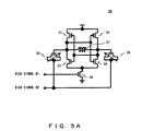
- A configuration example of an LC resonant oscillator (20) is shown in Fig. 5A.
- As shown in this figure, the source of a PMOS transistor (21) and that of a PMOS transistor (22) are connected to a power supply in common. The drain of the PMOS transistor (21) and that of the PMOS transistor (22) are connected to the drain of an NMOS transistor (23) and that of an NMOS transistor (24) respectively. The gate of the PMOS transistor (21) and that of the PMOS transistor (22) are connected to the gate of the NMOS transistor (23) and that of the NMOS transistor (24) respectively. The source of the NMOS transistor (23) and that of the NMOS transistor (24) are connected to the drain of an NMOS transistor (28) in common. The source of the NMOS transistor (28) is connected to a ground. To the gate of the NMOS transistor (28), a
bias signal # 1, which determines the common mode potential of an oscillation output node, is input. The drain of the PMOS transistor (21) and the gate of the PMOS transistor (22), and the gate of the PMOS transistor (21) and the drain of the PMOS transistor (22) are mutually connected. - Furthermore, an inductance element (27) is connected between the drain of the PMOS transistor (21) and that of the PMOS transistor (22). One of electrodes of a variable capacitive element (25) is connected to the drain of the PMOS transistor (21), whereas one of electrodes of a variable capacitive element (26) is connected to the drain of the PMOS transistor (22). A
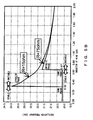
bias signal # 2, which controls the oscillation frequency of the LC resonant oscillator (20), is input to the other electrodes of the variable capacitive elements (25) and (26). Thisbias signal # 2 is equivalent to that shown in Fig. 4. - A resistor value of the resistor element (31) shown in Fig. 4 is described next with reference to Fig. 5B.
- Fig. 5B is a graph representing simulation results of an oscillation frequency in a model where two LC resonant oscillators (20) are connected with a wire having a resistor and an inductor. This graph shows a relationship between a resistor value R of the wire between the LC resonant oscillators (20) and the stability of the oscillation of the LC resonant oscillators (20).
- Namely, the oscillation frequency is stable at a frequency that slightly exceeds 20 GHz, but it sharply changes at and after an inductor value 0.32 nH when the resistor value R is 15 ohm, and at and after an inductor value 0.67 nH when the resistor value R is 75 ohm.
- According to this graph, the oscillation tends to be stable if the resistor value is large relative to the inductor component of the wire. From a different point of view, this graph represents that the oscillation becomes unstable at a certain inductor value or larger while the inductor component of the wire increases relative to a constant resistor value. Accordingly, it can be said that one factor which determines the stability of the oscillation is a ratio of the resistance to the inductance. Besides, the oscillation is proved to become stable if the inductor component of the wire can be substantially reduced relative to a constant resistor value.
- As the length of the wire becomes longer, the inductance of the wire and the resistance increase roughly in proportion to the length. Therefore, the value of the resistor to be inserted between the LC resonant oscillators (20) in the first preferred embodiment is determined according to the length of the wire.
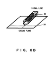
- Fig. 6A explains a second preferred embodiment, a physical structure of which reduces the inductance of a wire (30) that connects oscillation nodes of LC resonant oscillators #1 (20) and #2 (20). Preferably, the structure of the wire (30) that connects the oscillation nodes of the LC resonant oscillators #1 (20) and #2 (20) is a structure where the inductance of the wire becomes small as known from Fig. 5B. Therefore, a distance between a signal line and a ground plane connected to a fixed potential is made short, and ground lines similarly connected to a fixed potential are arranged on both sides of the signal line as shown in this figure.
- Figs. 6B and 6C show modification examples 1 and 2 of the wiring structure shown in Fig. 6A. The modification example 1 shown in Fig. 6B is a structure where a signal line is made extremely close to a ground plane. The signal line itself can be also a micro-strip line as a replacement for the modification example 1 shown in Fig. 6B.
- The modification example 2 shown in Fig. 6C is a structure where ground planes are arranged on both sides of a signal line. The signal line itself can be a strip line as a replacement for the modification example 2 shown in Fig. 6C.
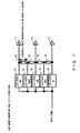
- Fig. 7 shows a third preferred embodiment of the present invention. In this preferred embodiment, auxiliary LC resonant oscillators #A1 (20) and #A2 (20), which have the same configuration as an LC resonant oscillator #1 (20) or the like, are arranged respectively between LC resonant oscillators #1 (20) and #2 (20), and between LC resonant oscillators #2 (20) and #3 (20), and their oscillation nodes are connected. As a result, an electric length between the oscillation nodes can be halved in comparison with a case where the auxiliary LC resonant oscillators #A1 (20) and #A2 (20) are not arranged, whereby an inductance between the oscillation nodes can be reduced.
- Fig. 8A shows a fourth preferred embodiment of the present invention, in which LC resonant oscillators are oscillated in synchronization by using injection locking. In this preferred embodiment, oscillation nodes of the LC resonant oscillators #1 (20) and #2 (20) are connected via a buffer (40), the LC resonant oscillator #2 (20) is oscillated by using injection locking, and the LC resonant oscillators #1 (20) and #2 (20) are oscillated in the same phase and at the same frequency.
- Additionally, in this preferred embodiment, a wire between the oscillation nodes is divided by the buffer, whereby the length of the wire, which exerts an influence on the oscillation of the LC resonant oscillators #1 (20) and #2 (20), becomes short, and the inductance between the oscillation nodes can be reduced in a similar manner as in the fourth preferred embodiment shown in Fig. 4.
- Fig. 8B shows a first modification example of the configuration shown in Fig. 8A. This example is a configuration where at least one LC resonant oscillator #2 (120) having an input terminal for coupling is used, an oscillation node of an LC resonant oscillator #1 (20) is connected via a buffer (40) to the input terminal for coupling of the LC resonant oscillator #2 (120) having the input terminal for coupling, and an oscillation signal of the LC resonant oscillator #1 (20) is injected to the LC resonant oscillator #2 (120), whereby the LC resonant oscillator #2 (120) is oscillated in the same phase and at the same frequency as the LC resonant oscillator #1 (20).
- Fig. 9 shows a second modification example where a plurality of buffers (40) shown in Fig. 8B are provided. As a matter of course, a plurality of buffers (40) can be provided also in the configuration shown in Fig. 8A. The second modification example produces the effect of, for instance, reducing the attenuation of a signal by shortening the substantial length of a wire when the length of the wire, for example, between LC resonant oscillators #1 (20) and #2 (120) to be connected is long.
- Fig. 10 shows a third modification example where at least one pair of LC resonant oscillators #1 (120) and #2 (120), which respectively have an input terminal for coupling, is used, and their oscillation nodes and input terminals for coupling are alternately connected via buffers (40) in a symmetrical manner. Such a symmetrical configuration is adopted, whereby a clock of higher precision can be distributed to each circuit block. Accordingly, it is effective to apply this modification example, for instance, to synchronization between the LC resonant oscillators #1 (120) and #2 (120) that supply a clock to circuit blocks operations of which require a clock of high precision.
- Fig. 11A shows a configuration example of an LC resonant oscillator (120) having input terminals for coupling. This example is a configuration where a serial circuit of a PMOS transistor (210) and an NMOS transistor (230), and a serial circuit of a PMOS transistor (220) and an NMOS transistor (240) are respectively connected in parallel to the serial circuit of the PMOS transistor (21) and the NMOS transistor (23), and the serial circuit of the PMOS transistor (22) and the NMOS transistor (24) of the LC resonant oscillator (20) shown in Fig. 5A, and the input terminals for coupling #1 (291) and #2 (292), which are intended to inject those oscillation signals as a differential signal, are provided at a connecting point of the PMOS transistor (210) and the NMOS transistor (230), and a connecting point of the PMOS transistor (220) and the NMOS transistor (240) respectively.
- Fig. 11B shows a configuration example 1 of a preferable buffer circuit used by the present invention. As shown in this figure, the drains of NMOS transistors (411) and (412) are connected to a power supply via resistor elements (413) and (414) respectively, and their sources are connected to the drain of an NMOS transistor (415) in common. The source of the NMOS transistor (415) is connected to a ground, and a bias signal which determines the common mode potential of a buffer output is input to the gate of the NMOS transistor (415).
- Input terminals are provided at the gates of the NMOS transistors (411) and (412), whereas output terminals are provided at the drains of the NMOS transistors (411) and (412).
- Fig. 11C shows a configuration example 2 of a preferable buffer circuit used by the present invention. As shown in this figure, a serial circuit of a PMOS transistor (421) and an NMOS transistor (423), gates of which are connected, and a serial circuit of a PMOS transistor (422) and an NMOS transistor (424), gates of which are connected in a similar manner, are connected in parallel between a power supply and the drain of an NMOS transistor (425). The source of the NMOS transistor (425) is connected to a ground, and a bias signal which determines the common mode potential of a buffer output is input to the gate of the NMOS transistor (425).
- Input terminals are provided at a connecting point of the gates of the PMOS transistor (421) and the NMOS transistor (423), and a connecting point of the gates of the PMOS transistor (422) and the NMOS transistor (424), whereas output terminals are provided at a connecting point of the drains of the PMOS transistor (421) and the NMOS transistor (423), and a connecting point of the drains of the PMOS transistor (422) and the NMOS transistor (424).
- Note that the configurations shown in Figs. 5A, 11A, 11B, and 11C are merely circuit examples. It is evident to a person skilled in the art that a variety of modification examples can be adopted other than the exemplified configurations.
Claims (13)
- A clock signal generating and distributing apparatus for generating a clock signal in an LC resonant voltage control oscillator(20) and for distributing the clock signal to a corresponding circuit(91,92) from an oscillation node of the LC resonant voltage control oscillator(20) arranged in each part within a chip by using the LC resonant voltage control oscillator(20) as a voltage control oscillator of a PLL, by arranging in each part within the chip the LC resonant voltage control oscillator(20) having the same configuration as the LC resonant voltage control oscillator(20), by connecting oscillation nodes of the LC resonant voltage control oscillators with a one-dimensional wire or wires in the shape of a mesh, and by distributing an oscillation frequency control signal generated by the PLL to each of the LC resonant voltage control oscillators(20).
- The clock signal generating and distributing apparatus according to claim 1, whereinan inductance of the wire connecting the oscillation nodes of the LC resonant voltage control oscillators(20) is set to a value at which the LC resonant voltage control oscillators(20) oscillate in the same phase.
- The clock signal generating and distributing apparatus according to claim 2, whereina resistor element(31) is inserted between the oscillation nodes, which are mutually connected, of the LC resonant voltage control oscillators(20).
- The clock signal generating and distributing apparatus according to claim 3, whereina resistance of the resistor element is implemented by an ON resistance of a transistor.
- The clock signal generating and distributing apparatus according to claim 2, whereinthe inductance of the wire connecting the oscillation nodes of the LC resonant voltage control oscillators(20) is set to a value at which the LC resonant voltage control oscillators(20) oscillate in the same phase by using a physical structure of the wire.
- The clock signal generating and distributing apparatus according to claim 5, whereinthe physical structure of the wire is a structure where a ground plane(39) or a ground line(33), which is connected to a fixed potential, is arranged close to the wire connecting the oscillation nodes of the LC resonant voltage control oscillators(20).
- The clock signal generating and distributing apparatus according to claim 5, whereinthe wire is a micro-strip line.
- The clock signal generating and distributing apparatus according to claim 5, whereinthe wire is a strip line.
- The clock signal generating and distributing apparatus according to claim 2, comprisingan LC resonant voltage control oscillator(20) an oscillation frequency of which is controlled by the oscillation frequency control signal generated by the PLL, an oscillation node of which is connected to the wire between the oscillation nodes of the LC resonant voltage control oscillators(20) connected with the one-dimensional wire or the wires in the shape of a mesh, and not connected to other circuits not via the wire.
- A clock signal generating and distributing apparatus for generating a clock signal in an LC resonant voltage control oscillator(20) and for distributing the clock signal to a corresponding circuit(91,92) from an oscillation node of the LC resonant voltage control oscillator(20) arranged in each part within a chip by using the LC resonant voltage control oscillator(20) as a voltage control oscillator(20) of a PLL, by arranging in each part within the chip the LC resonant voltage control oscillator(20) having the same configuration as the LC resonant voltage control oscillator(20), by distributing an oscillation frequency control signal generated by the PLL to each of the LC resonant voltage control oscillators(20), and by making the LC resonant voltage control oscillators(20) oscillate in synchronization by using injection locking.
- The clock signal generating and distributing apparatus according to claim 10, whereinthe oscillation nodes of the LC resonant voltage control oscillators(20) are connected with a one-dimensional wire or wires in the shape of a mesh, at least one buffer(40) is inserted on a wire connecting the oscillation nodes of the LC resonant voltage control oscillators(20), and an LC resonant voltage control oscillator(20) on an output side of the buffer(40) is synchronized with an LC resonant voltage control oscillator(20) on an input side of the buffer(40) by using injection locking.
- The clock signal generating and distributing apparatus according to claim 11, whereinan LC resonant voltage control oscillator(120) having an input terminal for coupling is used as at least one LC resonant voltage control oscillator(20) on the output side of the buffer(40), and the wire on the output side of the buffer(40) is connected to the input terminal for coupling as a replacement for the oscillation node.
- The clock signal generating and distributing apparatus according to claim 11, whereinLC resonant voltage control oscillators(120), which respectively have an input terminal for coupling, are used as at least one pair of LC resonant voltage control oscillators(20), and an oscillation node of one of the LC resonant voltage control oscillators(120) is connected to the input terminal for coupling of the other of the LC resonant voltage control oscillators(120) with a wire on which a buffer(40) is inserted.
Applications Claiming Priority (1)
| Application Number | Priority Date | Filing Date | Title |
|---|---|---|---|
| JP2005271058A JP4299283B2 (en) | 2005-09-16 | 2005-09-16 | Clock signal generation and distribution device |
Publications (2)
| Publication Number | Publication Date |
|---|---|
| EP1764669A2 true EP1764669A2 (en) | 2007-03-21 |
| EP1764669A3 EP1764669A3 (en) | 2014-03-26 |
Family
ID=37487661
Family Applications (1)
| Application Number | Title | Priority Date | Filing Date |
|---|---|---|---|
| EP06251534.1A Withdrawn EP1764669A3 (en) | 2005-09-16 | 2006-03-22 | Clock signal generating and distributing apparatus |
Country Status (3)
| Country | Link |
|---|---|
| US (1) | US7863987B2 (en) |
| EP (1) | EP1764669A3 (en) |
| JP (1) | JP4299283B2 (en) |
Cited By (6)
| Publication number | Priority date | Publication date | Assignee | Title |
|---|---|---|---|---|
| WO2011046984A2 (en) * | 2009-10-12 | 2011-04-21 | Cyclos Semiconductor Inc. | Architecture for single-stepping in resonant clock distribution networks |
| US8461873B2 (en) | 2007-05-23 | 2013-06-11 | Cyclos Semiconductor, Inc. | Resonant clock and interconnect architecture for digital devices with multiple clock networks |
| CN104105325A (en) * | 2013-04-15 | 2014-10-15 | 张妙娟 | DC low-voltage double-push injection phase-locking power synthesis electrodeless lamp |
| CN104105293A (en) * | 2013-04-15 | 2014-10-15 | 阮树成 | Direct-current low-voltage power supply four-push-pull injection-locking power synthesis electrodeless lamp group |
| CN104105257A (en) * | 2013-04-15 | 2014-10-15 | 张妙娟 | DC low-voltage double-push injection phase-locking light-emitting diode LED array lamp |
| CN107040229A (en) * | 2015-12-10 | 2017-08-11 | 泰连德国有限公司 | Filter assembly and high-tension connector assembly parts for high-tension connector assembly parts |
Families Citing this family (20)
| Publication number | Priority date | Publication date | Assignee | Title |
|---|---|---|---|---|
| WO2010057520A1 (en) * | 2008-11-18 | 2010-05-27 | Telefonaktiebolaget Lm Ericsson (Publ) | Method and arrangement for voltage controlled oscillator device |
| US20110050297A1 (en) * | 2009-08-28 | 2011-03-03 | Nel Frequency Controls, Inc. | System employing synchronized crystal oscillator-based clock |
| JP5387187B2 (en) | 2009-07-10 | 2014-01-15 | 富士通株式会社 | Clock signal distribution device |
| US20120161827A1 (en) * | 2010-12-28 | 2012-06-28 | Stmicroelectronics (Canada) Inc. | Central lc pll with injection locked ring pll or dell per lane |
| JPWO2012132847A1 (en) * | 2011-03-31 | 2014-07-28 | 株式会社半導体理工学研究センター | Injection-locked frequency-locked oscillator |
| US8362848B2 (en) * | 2011-04-07 | 2013-01-29 | Qualcomm Incorporated | Supply-regulated VCO architecture |
| US8390388B1 (en) * | 2011-08-17 | 2013-03-05 | Rockwell Collins, Inc. | Differential cancellation of vibration interference in oscillators |
| JP5811863B2 (en) * | 2012-01-26 | 2015-11-11 | 富士通株式会社 | Clock distributor and electronic device |
| JP5853870B2 (en) * | 2012-06-08 | 2016-02-09 | 富士通株式会社 | Clock distributor and electronic device |
| US9058130B2 (en) | 2013-02-05 | 2015-06-16 | International Business Machines Corporation | Tunable sector buffer for wide bandwidth resonant global clock distribution |
| US9054682B2 (en) | 2013-02-05 | 2015-06-09 | International Business Machines Corporation | Wide bandwidth resonant global clock distribution |
| US8704576B1 (en) | 2013-02-05 | 2014-04-22 | International Business Machines Corporation | Variable resistance switch for wide bandwidth resonant global clock distribution |
| CN104105324A (en) * | 2013-04-15 | 2014-10-15 | 张妙娟 | DC low-voltage power supply four-push injection phase-locking power synthesis fluorescent lamp group |
| CN104105327A (en) * | 2013-04-15 | 2014-10-15 | 阮小青 | Solar power supply double-push injection-locking power synthesis electrodeless lamp |
| JP6263906B2 (en) | 2013-08-28 | 2018-01-24 | 富士通株式会社 | Electronic circuit and control method |
| JP6171758B2 (en) * | 2013-09-10 | 2017-08-02 | 富士通株式会社 | High frequency signal generation circuit, transmission device, reception device, and transmission / reception device |
| US9270289B2 (en) * | 2014-02-13 | 2016-02-23 | Fujitsu Limited | Monolithic signal generation for injection locking |
| US9356608B1 (en) * | 2014-04-29 | 2016-05-31 | Microsemi Storage Solutions (U.S.), Inc. | Method and apparatus for controlling mismatch in a voltage controlled oscillator array |
| US10333531B2 (en) * | 2017-02-23 | 2019-06-25 | National Chung Cheng University | Synchronous oscillation circuit |
| CN110113007A (en) * | 2019-05-31 | 2019-08-09 | 华讯方舟科技有限公司 | A kind of injection locking oscillating circuit, frequency adjustment method and injection locked oscillator |
Family Cites Families (10)
| Publication number | Priority date | Publication date | Assignee | Title |
|---|---|---|---|---|
| JPH07221546A (en) | 1994-01-28 | 1995-08-18 | Nippon Telegr & Teleph Corp <Ntt> | Injection synchronization oscillator |
| JP3619352B2 (en) * | 1997-08-28 | 2005-02-09 | 株式会社ルネサステクノロジ | Semiconductor integrated circuit device |
| US6175285B1 (en) * | 1998-08-14 | 2001-01-16 | Lucent Technologies, Inc. | Injection tuned resonant circuits |
| JP4589559B2 (en) | 2000-04-13 | 2010-12-01 | 株式会社エッチャンデス | Synchronous oscillator circuit and oscillator circuit network |
| US6813721B1 (en) * | 2000-09-20 | 2004-11-02 | Stratus Computer Systems, S.A.R.L. | Methods and apparatus for generating high-frequency clocks deterministically from a low-frequency system reference clock |
| JP2002135114A (en) | 2000-10-24 | 2002-05-10 | Sony Corp | Phase synchronous circuit and generator using the same |
| US6617936B2 (en) * | 2001-02-20 | 2003-09-09 | Velio Communications, Inc. | Phase controlled oscillator |
| JP3795364B2 (en) | 2001-09-27 | 2006-07-12 | シャープ株式会社 | Integrated circuit and receiver |
| US6686785B2 (en) * | 2001-10-11 | 2004-02-03 | Sun Microsystems, Inc. | Deskewing global clock skew using localized DLLs |
| JP4040034B2 (en) * | 2004-05-28 | 2008-01-30 | 富士通株式会社 | Oscillator and semiconductor device |
-
2005
- 2005-09-16 JP JP2005271058A patent/JP4299283B2/en not_active Expired - Fee Related
-
2006
- 2006-03-22 EP EP06251534.1A patent/EP1764669A3/en not_active Withdrawn
- 2006-03-23 US US11/386,789 patent/US7863987B2/en not_active Expired - Fee Related
Non-Patent Citations (1)
| Title |
|---|
| None * |
Cited By (16)
| Publication number | Priority date | Publication date | Assignee | Title |
|---|---|---|---|---|
| US8461873B2 (en) | 2007-05-23 | 2013-06-11 | Cyclos Semiconductor, Inc. | Resonant clock and interconnect architecture for digital devices with multiple clock networks |
| US8502569B2 (en) | 2009-10-12 | 2013-08-06 | Cyclos Semiconductor, Inc. | Architecture for operating resonant clock network in conventional mode |
| US8593183B2 (en) | 2009-10-12 | 2013-11-26 | Cyclos Semiconductor, Inc. | Architecture for controlling clock characteristics |
| US8358163B2 (en) | 2009-10-12 | 2013-01-22 | Cyclos Semiconductor, Inc. | Resonant clock distribution network architecture for tracking parameter variations in conventional clock distribution networks |
| US8362811B2 (en) | 2009-10-12 | 2013-01-29 | Cyclos Semiconductor, Inc. | Architecture for single-stepping in resonant clock distribution networks |
| US8368450B2 (en) | 2009-10-12 | 2013-02-05 | Cyclos Semiconductor, Inc. | Architecture for adjusting natural frequency in resonant clock distribution networks |
| US8400192B2 (en) | 2009-10-12 | 2013-03-19 | Cyclos Semiconductor, Inc. | Architecture for frequency-scaled operation in resonant clock distribution networks |
| US8339209B2 (en) | 2009-10-12 | 2012-12-25 | Cyclos Semiconductor, Inc. | Method for selecting natural frequency in resonant clock distribution networks with no inductor overhead |
| WO2011046984A2 (en) * | 2009-10-12 | 2011-04-21 | Cyclos Semiconductor Inc. | Architecture for single-stepping in resonant clock distribution networks |
| WO2011046984A3 (en) * | 2009-10-12 | 2011-08-18 | Cyclos Semiconductor Inc. | Architecture for single-stepping in resonant clock distribution networks |
| US8659338B2 (en) | 2009-10-12 | 2014-02-25 | Cyclos Semiconductor, Inc. | Resonant clock distribution network architecture with programmable drivers |
| US9041451B2 (en) | 2009-10-12 | 2015-05-26 | Cyclos Semiconductor, Inc. | Resonant clock distribution network architecture for tracking parameter variations in conventional clock distribution networks |
| CN104105293A (en) * | 2013-04-15 | 2014-10-15 | 阮树成 | Direct-current low-voltage power supply four-push-pull injection-locking power synthesis electrodeless lamp group |
| CN104105257A (en) * | 2013-04-15 | 2014-10-15 | 张妙娟 | DC low-voltage double-push injection phase-locking light-emitting diode LED array lamp |
| CN104105325A (en) * | 2013-04-15 | 2014-10-15 | 张妙娟 | DC low-voltage double-push injection phase-locking power synthesis electrodeless lamp |
| CN107040229A (en) * | 2015-12-10 | 2017-08-11 | 泰连德国有限公司 | Filter assembly and high-tension connector assembly parts for high-tension connector assembly parts |
Also Published As
| Publication number | Publication date |
|---|---|
| US7863987B2 (en) | 2011-01-04 |
| JP4299283B2 (en) | 2009-07-22 |
| US20070063779A1 (en) | 2007-03-22 |
| EP1764669A3 (en) | 2014-03-26 |
| JP2007082158A (en) | 2007-03-29 |
Similar Documents
| Publication | Publication Date | Title |
|---|---|---|
| US7863987B2 (en) | Clock signal generating and distributing apparatus | |
| KR100348198B1 (en) | PLL circuit which can reduce phase offset without increase in operation voltage | |
| JP5387187B2 (en) | Clock signal distribution device | |
| JP3619352B2 (en) | Semiconductor integrated circuit device | |
| Kim et al. | A 20-GHz phase-locked loop for 40-gb/s serializing transmitter in 0.13-/spl mu/m CMOS | |
| US7301385B2 (en) | Methods and apparatus for managing clock skew | |
| US9899991B2 (en) | Circuits and methods of synchronizing differential ring-type oscillators | |
| US20170346444A1 (en) | Semiconductor Device and Method | |
| JP5583727B2 (en) | Voltage controlled oscillator with cascaded emitter follower buffer stages | |
| US10164570B2 (en) | Coupling structure for inductive device | |
| EP1764670B1 (en) | Clock distribution circuit | |
| US8981854B2 (en) | Clock distributor and electronic apparatus | |
| US9559635B2 (en) | Method and apparatus of synchronizing oscillators | |
| US10658975B2 (en) | Semiconductor device and method | |
| KR100808079B1 (en) | Clock signal generating and distributing apparatus | |
| US20130141178A1 (en) | Injection Locked Divider with Injection Point Located at a Tapped Inductor | |
| KR20040072083A (en) | Multi-phase clock generation circuit and method for reducing skew of clock signal | |
| KR100808076B1 (en) | Clock distribution circuit | |
| Ann et al. | Low power CMOS 8: 1 injection-locked frequency divider with LC cross-coupled oscillator | |
| KR100276083B1 (en) | Low noise divider for frequency synthesizer | |
| Ravinuthula et al. | REPLICA BASED" VCO GAIN AND LOOP FILTER'S JITTER REDUCTION TECHNIQUE FOR RING OSCILLATOR PLLS | |
| JP2000078004A (en) | Semiconductor integrated circuit device |
Legal Events
| Date | Code | Title | Description |
|---|---|---|---|
| PUAI | Public reference made under article 153(3) epc to a published international application that has entered the european phase |
Free format text: ORIGINAL CODE: 0009012 |
|
| AK | Designated contracting states |
Kind code of ref document: A2 Designated state(s): AT BE BG CH CY CZ DE DK EE ES FI FR GB GR HU IE IS IT LI LT LU LV MC NL PL PT RO SE SI SK TR |
|
| AX | Request for extension of the european patent |
Extension state: AL BA HR MK YU |
|
| RIC1 | Information provided on ipc code assigned before grant |
Ipc: G06F 1/10 20060101ALI20131018BHEP Ipc: G06F 1/04 20060101AFI20131018BHEP |
|
| PUAL | Search report despatched |
Free format text: ORIGINAL CODE: 0009013 |
|
| AK | Designated contracting states |
Kind code of ref document: A3 Designated state(s): AT BE BG CH CY CZ DE DK EE ES FI FR GB GR HU IE IS IT LI LT LU LV MC NL PL PT RO SE SI SK TR |
|
| AX | Request for extension of the european patent |
Extension state: AL BA HR MK YU |
|
| RIC1 | Information provided on ipc code assigned before grant |
Ipc: G06F 1/10 20060101ALI20140220BHEP Ipc: G06F 1/04 20060101AFI20140220BHEP |
|
| 17P | Request for examination filed |
Effective date: 20140826 |
|
| RBV | Designated contracting states (corrected) |
Designated state(s): AT BE BG CH CY CZ DE DK EE ES FI FR GB GR HU IE IS IT LI LT LU LV MC NL PL PT RO SE SI SK TR |
|
| AKX | Designation fees paid |
Designated state(s): DE FR GB |
|
| STAA | Information on the status of an ep patent application or granted ep patent |
Free format text: STATUS: EXAMINATION IS IN PROGRESS |
|
| 17Q | First examination report despatched |
Effective date: 20161130 |
|
| STAA | Information on the status of an ep patent application or granted ep patent |
Free format text: STATUS: THE APPLICATION IS DEEMED TO BE WITHDRAWN |
|
| 18D | Application deemed to be withdrawn |
Effective date: 20180529 |