EP1758171A1 - Vertical gallium nitride semiconductor device and epitaxial substrate - Google Patents
Vertical gallium nitride semiconductor device and epitaxial substrate Download PDFInfo
- Publication number
- EP1758171A1 EP1758171A1 EP06714948A EP06714948A EP1758171A1 EP 1758171 A1 EP1758171 A1 EP 1758171A1 EP 06714948 A EP06714948 A EP 06714948A EP 06714948 A EP06714948 A EP 06714948A EP 1758171 A1 EP1758171 A1 EP 1758171A1
- Authority
- EP
- European Patent Office
- Prior art keywords
- gallium nitride
- epitaxial film
- type conductivity
- substrate
- support base
- Prior art date
- Legal status (The legal status is an assumption and is not a legal conclusion. Google has not performed a legal analysis and makes no representation as to the accuracy of the status listed.)
- Withdrawn
Links
Images

Classifications
-
- H—ELECTRICITY
- H10—SEMICONDUCTOR DEVICES; ELECTRIC SOLID-STATE DEVICES NOT OTHERWISE PROVIDED FOR
- H10D—INORGANIC ELECTRIC SEMICONDUCTOR DEVICES
- H10D62/00—Semiconductor bodies, or regions thereof, of devices having potential barriers
- H10D62/80—Semiconductor bodies, or regions thereof, of devices having potential barriers characterised by the materials
- H10D62/81—Semiconductor bodies, or regions thereof, of devices having potential barriers characterised by the materials of structures exhibiting quantum-confinement effects, e.g. single quantum wells; of structures having periodic or quasi-periodic potential variation
-
- H—ELECTRICITY
- H10—SEMICONDUCTOR DEVICES; ELECTRIC SOLID-STATE DEVICES NOT OTHERWISE PROVIDED FOR
- H10D—INORGANIC ELECTRIC SEMICONDUCTOR DEVICES
- H10D30/00—Field-effect transistors [FET]
- H10D30/60—Insulated-gate field-effect transistors [IGFET]
- H10D30/64—Double-diffused metal-oxide semiconductor [DMOS] FETs
- H10D30/66—Vertical DMOS [VDMOS] FETs
-
- H—ELECTRICITY
- H10—SEMICONDUCTOR DEVICES; ELECTRIC SOLID-STATE DEVICES NOT OTHERWISE PROVIDED FOR
- H10D—INORGANIC ELECTRIC SEMICONDUCTOR DEVICES
- H10D62/00—Semiconductor bodies, or regions thereof, of devices having potential barriers
- H10D62/10—Shapes, relative sizes or dispositions of the regions of the semiconductor bodies; Shapes of the semiconductor bodies
- H10D62/13—Semiconductor regions connected to electrodes carrying current to be rectified, amplified or switched, e.g. source or drain regions
- H10D62/149—Source or drain regions of field-effect devices
- H10D62/151—Source or drain regions of field-effect devices of IGFETs
- H10D62/156—Drain regions of DMOS transistors
- H10D62/157—Impurity concentrations or distributions
-
- H—ELECTRICITY
- H10—SEMICONDUCTOR DEVICES; ELECTRIC SOLID-STATE DEVICES NOT OTHERWISE PROVIDED FOR
- H10D—INORGANIC ELECTRIC SEMICONDUCTOR DEVICES
- H10D8/00—Diodes
- H10D8/411—PN diodes having planar bodies
-
- H—ELECTRICITY
- H10—SEMICONDUCTOR DEVICES; ELECTRIC SOLID-STATE DEVICES NOT OTHERWISE PROVIDED FOR
- H10D—INORGANIC ELECTRIC SEMICONDUCTOR DEVICES
- H10D8/00—Diodes
- H10D8/60—Schottky-barrier diodes
-
- H—ELECTRICITY
- H10—SEMICONDUCTOR DEVICES; ELECTRIC SOLID-STATE DEVICES NOT OTHERWISE PROVIDED FOR
- H10D—INORGANIC ELECTRIC SEMICONDUCTOR DEVICES
- H10D62/00—Semiconductor bodies, or regions thereof, of devices having potential barriers
- H10D62/80—Semiconductor bodies, or regions thereof, of devices having potential barriers characterised by the materials
- H10D62/85—Semiconductor bodies, or regions thereof, of devices having potential barriers characterised by the materials being Group III-V materials, e.g. GaAs
- H10D62/8503—Nitride Group III-V materials, e.g. AlN or GaN
Definitions
- the present invention relates to vertical gallium nitride semiconductor devices and epitaxial substrates.
- Patent Document 1 a gallium nitride single crystal growth process is disclosed. According to this process, a gallium nitride single-crystal growth process enabling oxygen to be taken in as an n-type dopant is afforded.
- a gallium nitride single-crystal growth process enabling oxygen to be taken in as an n-type dopant is afforded.
- gallium nitride crystal is vapor-deposited, with the front side apart from the c-plane being kept intact, to dope oxygen into the gallium nitride crystal through the front side.
- gallium nitride crystal is vapor-deposited along the c-axis, with a facet plane apart from the c-plane being created and the facet plane being kept intact, to dope oxygen into the gallium nitride crystal through the facet plane.
- Non-Patent Document 1 describes characteristics of pin diodes.
- an (undoped, n ⁇ 3 ⁇ 10 16 cm -3 , 3 micrometers) gallium nitride epitaxial film and a (Mg-doped, p ⁇ 1 ⁇ 10 17 cm -3 , 0.3 micrometers) gallium nitride epitaxial film are fabricated by metalorganic vapor deposition onto a gallium nitride freestanding substrate, and on the back side of the gallium nitride freestanding substrate, an ohmic electrode for the n-type is fabricated, and on the front side of the epitaxial film, an ohmic electrode for the p-type.
- Patent Document 1 Japanese Unexamined Pat. App. Pub. No. 2002-373864 .
- Non-Patent Document 1 Irokawa et al., Applied Physics Letters, Vol. 83, 15 September 2003, pp. 2271-2273 .
- an n-type gallium nitride film is epitaxially grown on the n-type gallium nitride substrate.
- unintentional impurities such as magnesium (Mg) and iron (Fe) were concentrated in the vicinity of the interface between the gallium nitride substrate and the epitaxial film (a width of 1 ⁇ m or less). Peak concentration of these impurities is on the order of 10 17 cm -3 , and this impurity peak makes it difficult to provide a gallium nitride film having a designed low carrier concentration at a region in the vicinity of the interface.
- Impurities such magnesium (Mg), beryllium (Be), calcium (Ca), zinc (Zn), cadmium (Cd), iron (Fe), titanium (Ti), cobalt (Co), nickel (Ni), vanadium (V), chromium (Cr), or manganese (Mn) reduce carriers in the vicinity of the interface between the gallium nitride substrate and the epitaxial film, and make the region in the vicinity of the interface highly resistant. Therefore, it is desirable to provide an epitaxial film having a low carrier concentration on an n-type gallium nitride substrate.
- An object of the present invention brought about taking the above-described circumstances into consideration, is to make available vertical gallium nitride semiconductor devices and epitaxial substrates for the vertical gallium nitride semiconductor devices whose structure makes it possible to realize n-type gallium nitride films having a desired low carrier concentration on n-type gallium nitride substrates.
- One aspect of the present invention involves a vertical gallium nitride semiconductor device furnished with: (a) a gallium nitride support base of n + -type conductivity; (b) a gallium nitride epitaxial film of n-type conductivity provided on a principal surface of the gallium nitride support base; (c) a gate insulating film provided on the gallium nitride epitaxial film; (d) a gate electrode provided on the gate insulating film; (e) a p-type conductivity region provided in the gallium nitride epitaxial film; (f) an n-type conductivity region provided in the p-type conductivity region; (g) a source electrode provided on the n-type conductivity region of the gallium nitride epitaxial film; and (h) a drain electrode provided on a back side of the gallium nitride support base.
- a layer region is provided in the surface of the gallium nitride support base and the gallium nitride epitaxial film in which concentration of donor impurity along an axis from the gallium nitride support base to the gallium nitride epitaxial film is 1 ⁇ 10 18 cm -3 or more, and the donor impurity is at least either silicon or germanium.
- Another aspect of the present invention involves a vertical gallium nitride semiconductor device furnished with: (a) a gallium nitride support base of n-type conductivity; (b) a gallium nitride epitaxial film of n-type conductivity provided on a principal surface of the gallium nitride support base; (c) a Schottky electrode provided on the gallium nitride epitaxial film; and (d) an ohmic electrode provided on a back side of the gallium nitride support base.
- a layer region is provided in the surface of the gallium nitride support base and the gallium nitride epitaxial film in which concentration of donor impurity along an axis from the gallium nitride support base to the gallium nitride epitaxial film is 1 ⁇ 10 18 cm -3 or more, and the donor impurity is at least either silicon or germanium.
- a still further aspect of the present invention involves a vertical gallium nitride semiconductor device furnished with: (a) a gallium nitride support base of n-type conductivity; (b) a gallium nitride epitaxial film of n-type conductivity provided on a principal surface of the gallium nitride support base; (c) a gallium nitride epitaxial film of p-type conductivity provided on the gallium nitride epitaxial film of n-type conductivity; (d) a first ohmic electrode provided on the gallium nitride epitaxial film of p-type conductivity; and (e) a second ohmic electrode provided on a back side of the gallium nitride support base.
- a layer region is provided in the surface of the gallium nitride support base and the gallium nitride epitaxial film of n-type conductivity in which concentration of donor impurity along an axis from the gallium nitride support base to the gallium nitride epitaxial film of n-type conductivity is 1 ⁇ 10 18 cm -3 or more, and the donor impurity is at least either silicon or germanium.
- the donor impurity concentration profile of the layer region is 1 ⁇ 10 18 cm -3 or more, it is possible to reduce the decrease in the carrier concentration due to impurities such as magnesium (Mg) and iron (Fe) in the vicinity of the interface between the gallium nitride substrate and the epitaxial film.
- donor concentration of the gallium nitride epitaxial film is 5 ⁇ 10 17 cm -3 or less, and the donor impurity of the gallium nitride support base includes oxygen or silicon.
- a depletion layer can be sufficiently formed in the gallium nitride epitaxial film, and it is possible to reduce the decrease in the carrier in the vicinity of the interface between the gallium nitride substrate and the epitaxial film.
- a peak in the concentration profile of magnesium, beryllium, calcium, zinc, or cadmium resides in the layer region.
- the decrease in the carrier due to magnesium, beryllium, calcium, zinc, or cadmium serving as p type dopant can be reduced in the vicinity of the interface between the gallium nitride substrate and the epitaxial film.
- a peak in the concentration profile of iron, titanium, cobalt, nickel, vanadium, chromium, or manganese resides in the layer region.
- the carrier decrease originating in iron, titanium, cobalt, nickel, vanadium, chromium, or manganese, which act as lifetime killers, can be reduced in the vicinity of the interface between the gallium nitride substrate and the epitaxial film.
- a still further aspect of the present invention involves an epitaxial substrate furnished with: (a) a gallium nitride substrate of n-type conductivity; and (b) a gallium nitride epitaxial film of n-type conductivity provided on the gallium nitride substrate.
- a layer region is provided in the surface of the gallium nitride substrate and the gallium nitride epitaxial film in which concentration of donor impurity along an axis from the gallium nitride substrate to the gallium nitride epitaxial film is 1 ⁇ 10 18 cm -3 or more, and the donor impurity is at least either silicon or germanium.
- a still further aspect of the present invention involves an epitaxial substrate furnished with: (a) a gallium nitride substrate of n-type conductivity; (b) a gallium nitride epitaxial film of n-type conductivity provided on the gallium nitride substrate; and (c) a gallium nitride epitaxial film of p-type conductivity provided on the gallium nitride epitaxial film of n-type conductivity.
- a layer region is provided in the surface of the gallium nitride substrate and the gallium nitride epitaxial film in which concentration of donor impurity along an axis from the gallium nitride substrate to the gallium nitride epitaxial film of n-type conductivity is 1 ⁇ 10 18 cm -3 or more, and the donor impurity is at least either silicon or germanium.
- the epitaxial substrate since the donor impurity concentration profile of the layer region is 1 ⁇ 10 18 cm -3 or more, it is possible to reduce the decrease in the carrier concentration due to impurities such as magnesium (Mg) and iron (Fe) in the vicinity of the interface between the gallium nitride substrate and the epitaxial film. Consequently, the epitaxial substrate for the vertical gallium nitride semiconductor device is made available.
- impurities such as magnesium (Mg) and iron (Fe) in the vicinity of the interface between the gallium nitride substrate and the epitaxial film. Consequently, the epitaxial substrate for the vertical gallium nitride semiconductor device is made available.
- donor concentration of the gallium nitride epitaxial film is 5 ⁇ 10 17 cm -3 or less, and the gallium nitride substrate includes oxygen or silicon as a donor impurity.
- a depletion layer can be sufficiently formed in the gallium nitride epitaxial film, and it is possible to reduce the decrease in the carrier in the vicinity of the interface between the gallium nitride substrate and the epitaxial film.
- a peak in the concentration profile of magnesium, beryllium, calcium, zinc, or cadmium resides in the layer region.
- the carrier decrease originating in magnesium, beryllium, calcium, zinc, or cadmium, which act as p-type dopants, can be reduced in the vicinity of the interface between the gallium nitride substrate and the epitaxial film.
- a peak in the concentration profile of iron, titanium, cobalt, nickel, vanadium, chromium, or manganese resides in the layer region.
- the decrease in the carrier due to iron, titanium, cobalt, nickel, vanadium, chromium, or manganese serving as a lifetime killer can be reduced in the vicinity of the interface between the gallium nitride substrate and the epitaxial film.
- a vertical gallium nitride semiconductor device is made available that has a structure in which a gallium nitride film of n - type having a desired low carrier concentration on a gallium nitride substrate of n type. Furthermore, according to the present invention, an epitaxial substrate for the vertical gallium nitride semiconductor device is made available.
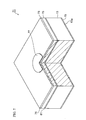
- Fig. 1 is a view of a Schottky diode.
- the Schottky diode 11 is made up of a gallium nitride support base 13 of n + -type conductivity, a gallium nitride epitaxial film 15 of n-type conductivity, a Schottky electrode 17, and an ohmic electrode 19.
- the gallium nitride epitaxial film 15 is provided on the principal surface of the gallium nitride support base 13.
- the Schottky electrode 17 is provided on the gallium nitride epitaxial film 15.
- the ohmic electrode 19 is provided on a back side 13a of the gallium nitride support base 13.
- a layer region 21 is provided in the gallium nitride support base 13 and the gallium nitride epitaxial film 15. An interface between the gallium nitride support base 13 and the gallium nitride epitaxial film 15 is positioned in the layer region 21.
- donor impurity along an axis from the gallium nitride support base 13 to the gallium nitride epitaxial film 15 is 1 ⁇ 10 18 cm -3 or more.
- the donor impurity is at least either silicon or germanium.
- a concentration profile of the donor impurity of the layer region 21 has a peak value of 1 ⁇ 10 18 cm -3 or more, so that decrease in the carrier concentration due to impurities such as magnesium (Mg) and iron (Fe) in the vicinity of the interface between the gallium nitride substrate and the epitaxial film can be reduced.
- the donor concentration of the gallium nitride epitaxial film 15 may be 5 ⁇ 10 17 cm -3 or less, and the gallium nitride support base 13 may contain oxygen as a donor impurity. Alternatively, the gallium nitride support base 13 may contain silicon as a donor impurity. According to the Schottky diode, a depletion layer can be sufficiently formed in the gallium nitride epitaxial film 15, and the decrease in the carrier concentration in the vicinity of the interface between the gallium nitride support base and the epitaxial film can be reduced.
- an epitaxial substrate was manufactured.
- a gallium nitride (GaN) freestanding substrate manufactured by HVPE method was prepared.
- the GaN freestanding substrate had a principal surface of (0001) plane, and showed n + conductivity.
- the substrate had a carrier concentration of 3 ⁇ 10 18 cm -3 and a thickness of 400 ⁇ m.
- the average dislocation density in the substrate was 1 ⁇ 10 6 cm -2 or less.
- a GaN epitaxial film was grown on the principal surface of the freestanding substrate by metal organic chemical vapor deposition.
- the epitaxial film had n-type conductivity.
- the film had a carrier concentration of 5 ⁇ 10 15 cm -3 and a thickness of 3.3 ⁇ m.
- silicon could be added to the surface layer of the substrate or the epitaxial film.
- a Schottky diode was manufactured following a procedure described hereinafter.
- an ohmic electrode was formed on the whole area of the back side of the GaN freestanding substrate.
- the ohmic electrode was composed of Ti/Al/Ti/Au (20 nm/100 nm/20 nm/300 nm).
- an alloying process was performed (at 600 degrees Celsius, for one minute).
- a Schottky electrode was formed on the surface of the epitaxial film.
- the Schottky electrode was an Au film having a diameter of 200 ⁇ m, for example.
- a metallic film was deposited by resistance heating deposition.
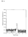
- Fig. 2 is a graph plotting the magnesium (Mg) concentration in the above-described epitaxial substrate by secondary ion mass spectrometry.
- a peak of the concentration curve C Mg was positioned in the vicinity of the interface between the gallium nitride substrate and the epitaxial film.
- the peak concentration was 1 ⁇ 10 16 cm -3 or less.
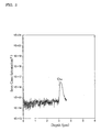
- Fig. 3 is a graph plotting the iron (Fe) concentration in the above-described epitaxial substrate by secondary ion mass spectrometry.
- a peak of the concentration curve C Fe was positioned in the vicinity of the interface between the gallium nitride substrate and the epitaxial film.
- the peak concentration was 1 ⁇ 10 17 cm -3 or less.
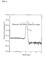
- Fig. 4 is a graph plotting the donor concentration (silicon) in the layer region of the above-described epitaxial substrate by secondary ion mass spectrometry.
- a peak of the concentration curve C Si was positioned in the vicinity of the interface between the gallium nitride substrate and the epitaxial film. Since the donor impurity concentration profile of the layer region had a peak value of 1 ⁇ 10 18 cm -3 or more, decrease in the carrier concentration due to impurities such as magnesium (Mg) and iron (Fe) in the vicinity of the interface between the gallium nitride substrate and the epitaxial film can be reduced. Although the thickness of the layer region was larger than a width of distribution of the above-described impurities, it was 1 ⁇ m or less, for example.
- Be beryllium
- Ca calcium
- Zn zinc
- Cd cadmium
- Ti titanium
- Co cobalt
- Ni nickel
- vanadium V
- Cr chromium
- Mn manganese
- Mg magnesium
- Fe iron
- Fig. 5 is a view depicting a vertical transistor.
- the vertical transistor 41 is made up of a gallium nitride support base 43 of n + -type conductivity, a gallium nitride epitaxial film 45 of n-type conductivity, a gate electrode 47, a p-type conductivity region 49, an n-type conductivity region 51, a source electrode 53, and a drain electrode 55.
- the gallium nitride epitaxial film 45 is provided on the principal surface of the gallium nitride support base 43.
- the gate electrode 47 is provided on the gallium nitride epitaxial film 45. Below the gate electrode 47 is provided an extended portion 49b of the p-type conductivity region 49.
- the p-type conductivity region 49 is provided in the gallium nitride epitaxial film 45.
- the n-type conductivity region 51 is provided in the p-type conductivity region 49.
- the source electrode 53 is provided on the n-type conductivity region 51 in the gallium nitride epitaxial film 45.
- the drain electrode 55 is provided on a back side 43a of the gallium nitride support base 43.
- a gate insulating film 59 is provided between the gallium nitride epitaxial film 45 and the gate electrode 47.
- a silicon dioxide film, a silicon oxynitride film, a silicon nitride film, alumina, aluminum nitride, AlGaN can be used as a material for the gate insulating film 59.
- a layer region 57 is provided in the gallium nitride support base 43 and the gallium nitride epitaxial film 45.
- An interface between the gallium nitride support base 43 and the gallium nitride epitaxial film 45 is positioned in the layer region 57.
- donor impurity along an axis from the gallium nitride support base 43 to the gallium nitride epitaxial film 45 is 1 ⁇ 10 18 cm -3 or more.
- the donor impurity is at least either silicon or germanium.
- a concentration profile of the donor impurity of the layer region 57 has a peak value of 1 ⁇ 10 18 cm -3 or more, so that the decrease in the carrier due to impurities such as magnesium (Mg) and iron (Fe) in the vicinity of the interface between the gallium nitride support base and the epitaxial film can be reduced. It can reduce the decrease in the carrier concentration due to impurities such as beryllium (Be), calcium (Ca), zinc (Zn), cadmium (Cd), titanium (Ti), cobalt (Co), nickel (Ni), vanadium (V), chromium (Cr), and manganese (Mn) as well as magnesium (Mg) and iron (Fe).
- impurities such as beryllium (Be), calcium (Ca), zinc (Zn), cadmium (Cd), titanium (Ti), cobalt (Co), nickel (Ni), vanadium (V), chromium (Cr), and manganese (Mn) as well as magnesium (M
- the gallium nitride vertical electronic devices 11 and 41 include the homoepitaxial films 15 and 45 of low concentration on the gallium nitride substrate 13 and 43, respectively.
- the impurities such as magnesium and iron are likely to be concentrated in the vicinity of the interface between the gallium nitride substrate and the homoepitaxial film, it is difficult to control the carrier concentration in the vicinity of the interface, where the concentration is low. Therefore, the present invention makes use of the layer region having a relatively high concentration provided in the vicinity of the interface in order to reduce the affect of the above-descried impurities and to maintain the carrier concentration of the epitaxial film apart from the interface to a desired low concentration. Furthermore, it is possible to remove the electrical affects due to the affects by the impurities, so that forward resistance or on-resistance of the gallium nitride vertical electronic devices 11 and 41 can be reduced and the backward breakdown voltage can be improved.
- Fig. 6 is a view depicting an epitaxial substrate.
- the epitaxial substrate 61 is manufactured according to a following process.
- the epitaxial substrate 61 is made up of a gallium nitride substrate 63 of n + -type conductivity, and a gallium nitride epitaxial film 65 of n-type conductivity.
- the gallium nitride epitaxial film 65 is provided on the gallium nitride substrate 63.
- a layer region 67 is provided in the gallium nitride substrate 63 and the gallium nitride epitaxial film 65.
- An interface between the gallium nitride substrate 63 and the gallium nitride epitaxial film 65 is positioned in the layer region 67.
- donor impurity along an axis from the gallium nitride substrate 63 to the gallium nitride epitaxial film 65 has a peak value of 1 ⁇ 10 18 cm -3 or more.
- the donor impurity is at least either silicon or germanium.
- a concentration profile of the donor impurity of the layer region 67 has a peak value of 1 ⁇ 10 18 cm -3 or more, so that it is possible to reduce the decrease in the carrier concentration due to impurities such as magnesium (Mg) and iron (Fe) in the vicinity of the interface between the gallium nitride substrate and the epitaxial film. Furthermore, it can reduce the decrease in the carrier concentration due to impurities such as beryllium (Be), calcium (Ca), zinc (Zn), cadmium (Cd), titanium (Ti), cobalt (Co), nickel (Ni), vanadium (V), chromium (Cr), and manganese (Mn) as well as magnesium (Mg) and iron (Fe).
- impurities such as beryllium (Be), calcium (Ca), zinc (Zn), cadmium (Cd), titanium (Ti), cobalt (Co), nickel (Ni), vanadium (V), chromium (Cr), and manganese (Mn) as well
- the donor concentration of the gallium nitride epitaxial film 65 may be 5 ⁇ 10 17 cm -3 or less, and the donor impurity of the gallium nitride substrate 63 may contain oxygen. Alternatively, the donor impurity of the gallium nitride substrate 63 may contain silicon. According to the epitaxial substrate 61, a depletion layer can be sufficiently formed in the gallium nitride epitaxial film 65, and it is possible to reduce the decrease in the carrier concentration in the vicinity of the interface between the gallium nitride substrate and the epitaxial film, so that the epitaxial substrate 61 is preferable to gallium nitride vertical semiconductor devices having a high breakdown voltage.
- Fig. 7 is a view depicting a pn junction diode.
- the pn junction diode 71 is made up of a gallium nitride support base 13 of n-type conductivity, a gallium nitride epitaxial film 73 of p-type conductivity, a gallium nitride epitaxial film 75 of n-type conductivity, a first ohmic electrode 77, and a second ohmic electrode 79.
- the gallium nitride epitaxial film 75 of n-type conductivity is provided on the principal surface of the gallium nitride support base 13.
- the gallium nitride epitaxial film 73 of p-type conductivity is provided on the gallium nitride epitaxial film 75 of n-type conductivity.
- the first ohmic electrode 77 is provided on the gallium nitride epitaxial film 73 of p-type conductivity.
- the second ohmic electrode 79 is provided on a back side 13a of the gallium nitride support base 13.
- the gallium nitride epitaxial film 73 of p-type conductivity and the gallium nitride epitaxial film 75 of n-type conductivity constitute a pn junction 76.
- Concentration of donor impurity along an axis from the gallium nitride support base 13 to the gallium nitride epitaxial film 73 is 1 ⁇ 10 18 cm -3 or more.
- the layer region 81 is provided in the surface of the gallium nitride support base 13 and the gallium nitride epitaxial film 75 of n-type conductivity.
- the donor impurity is at least either silicon or germanium.
- the donor impurity concentration profile of the layer region 81 is 1 ⁇ 10 18 cm -3 or more, so that it is possible to reduce the decrease in the carrier concentration due to impurities such as magnesium (Mg) and iron (Fe) in the vicinity of the interface between the gallium nitride support base and the epitaxial film.
- the donor concentration of the gallium nitride epitaxial film 75 may be 5 ⁇ 10 17 cm -3 or less.
- An epitaxial substrate was manufactured according to a following process.
- a gallium nitride (GaN) freestanding substrate manufactured by HVPE method was prepared.
- the GaN substrate has a principal surface of (0001) plain in the plane orientation.
- the GaN substrate has n + conductivity.
- the substrate had a carrier concentration of 3 ⁇ 10 18 cm -3 and a thickness of 400 ⁇ m.
- the average dislocation density in the substrate is 1 ⁇ 10 6 cm -2 or less.
- a GaN epitaxial film was grown on the principal surface of the freestanding substrate by metal organic chemical vapor deposition.
- the epitaxial film had n - conductivity.
- the film had a carrier concentration of 5 ⁇ 10 15 cm -3 and a thickness of 10 ⁇ m.
- the GaN epitaxial film On the GaN epitaxial film was provided a first gallium nitride epitaxial film of p-type conductivity.
- the first gallium nitride epitaxial film of p-type conductivity had a magnesium concentration of 1 ⁇ 10 18 cm -3 and a thickness of 0. 5 ⁇ m.
- a second gallium nitride epitaxial film of p-type conductivity On the second gallium nitride epitaxial film of p-type conductivity was provided a second gallium nitride epitaxial film of p-type conductivity.
- the second gallium nitride epitaxial film of p-type conductivity had a magnesium concentration of 5 ⁇ 10 19 cm -3 and a thickness of 0. 05 ⁇ m.
- an n + GaN layer region having silicon of 5 ⁇ 10 18 cm -3 or more At an interface of the GaN freestanding substrate and the GaN epitaxial layer was provided an n + GaN layer region having silicon of 5 ⁇ 10 18 cm -3 or more. In order to form the layer region, silicon could be added into the surface of the substrate or the epitaxial film.
- a pn diode was manufactured according to a following procedure.
- an ohmic electrode was formed on an overall surface of the back side of the GaN freestanding substrate.
- an alloying process was performed. The alloying process was performed at 600 degrees Celsius for one minute, for example.
- an ohmic electrode was formed on the epitaxial film. The ohmic electrode had a radius of 200 ⁇ m, for example.
- an alloying process was performed. The alloying process was performed at 600 degrees Celsius for one minute.
- Peaks of Mg and Fe were detected in the vicinity of the interface between the epitaxial layer and the substrate by SIMS method.
- the peak concentration of magnesium was 1 ⁇ 10 16 cm -3 or less
- the peak concentration of iron was 1 ⁇ 10 17 cm -3 or less.
- the gallium nitride vertical electronic device (the gallium nitride pn junction diode 71, for example) includes the homoepitaxial film 75 of low concentration on the gallium nitride substrate 13.
- the present invention makes use of the layer region having a relatively high concentration provided in the vicinity of the interface to reduce the effects by the impurities and to maintain the carrier concentration of the epitaxial film apart from the interface to a desired low concentration.
- n type donor impurities can be added during the growth in the embodiment, they can exist in the substrate (on the surface and/or inside of the substrate) in advance of the epitaxial growth. Accordingly, rights on all modifications and alternations deriving from the scope of claims and the spirit of that scope are claimed.
Landscapes
- Electrodes Of Semiconductors (AREA)
- Crystals, And After-Treatments Of Crystals (AREA)
- Recrystallisation Techniques (AREA)
Abstract
Description
- The present invention relates to vertical gallium nitride semiconductor devices and epitaxial substrates.
- In
Patent Document 1, a gallium nitride single crystal growth process is disclosed. According to this process, a gallium nitride single-crystal growth process enabling oxygen to be taken in as an n-type dopant is afforded. In this process, using a seed crystal having the plane apart from the c-plane on the front side (top side), while a source gas including raw-material gallium, raw-material nitrogen, and oxygen for doping is supplied, gallium nitride crystal is vapor-deposited, with the front side apart from the c-plane being kept intact, to dope oxygen into the gallium nitride crystal through the front side. In another instance, using a seed crystal having the c-plane on the front side, while a source gas including raw-material gallium, raw-material nitrogen, and oxygen for doping is supplied, gallium nitride crystal is vapor-deposited along the c-axis, with a facet plane apart from the c-plane being created and the facet plane being kept intact, to dope oxygen into the gallium nitride crystal through the facet plane. - Non-Patent
Document 1 describes characteristics of pin diodes. In these diodes an (undoped, n ~ 3 × 1016 cm-3, 3 micrometers) gallium nitride epitaxial film and a (Mg-doped, p ~ 1 × 1017 cm-3, 0.3 micrometers) gallium nitride epitaxial film are fabricated by metalorganic vapor deposition onto a gallium nitride freestanding substrate, and on the back side of the gallium nitride freestanding substrate, an ohmic electrode for the n-type is fabricated, and on the front side of the epitaxial film, an ohmic electrode for the p-type.
Patent Document 1:Japanese Unexamined Pat. App. Pub. No. 2002-373864
Non-Patent Document 1: Irokawa et al., Applied Physics Letters, Vol. 83, 15 September 2003, pp. 2271-2273. - In the gallium nitride vertical electronic device, an n-type gallium nitride film is epitaxially grown on the n-type gallium nitride substrate. According to experiments by the inventors, it was found that unintentional impurities such as magnesium (Mg) and iron (Fe) were concentrated in the vicinity of the interface between the gallium nitride substrate and the epitaxial film (a width of 1 µm or less). Peak concentration of these impurities is on the order of 1017 cm-3, and this impurity peak makes it difficult to provide a gallium nitride film having a designed low carrier concentration at a region in the vicinity of the interface. Impurities such magnesium (Mg), beryllium (Be), calcium (Ca), zinc (Zn), cadmium (Cd), iron (Fe), titanium (Ti), cobalt (Co), nickel (Ni), vanadium (V), chromium (Cr), or manganese (Mn) reduce carriers in the vicinity of the interface between the gallium nitride substrate and the epitaxial film, and make the region in the vicinity of the interface highly resistant. Therefore, it is desirable to provide an epitaxial film having a low carrier concentration on an n-type gallium nitride substrate.
- An object of the present invention, brought about taking the above-described circumstances into consideration, is to make available vertical gallium nitride semiconductor devices and epitaxial substrates for the vertical gallium nitride semiconductor devices whose structure makes it possible to realize n-type gallium nitride films having a desired low carrier concentration on n-type gallium nitride substrates.
- One aspect of the present invention involves a vertical gallium nitride semiconductor device furnished with: (a) a gallium nitride support base of n+-type conductivity; (b) a gallium nitride epitaxial film of n-type conductivity provided on a principal surface of the gallium nitride support base; (c) a gate insulating film provided on the gallium nitride epitaxial film; (d) a gate electrode provided on the gate insulating film; (e) a p-type conductivity region provided in the gallium nitride epitaxial film; (f) an n-type conductivity region provided in the p-type conductivity region; (g) a source electrode provided on the n-type conductivity region of the gallium nitride epitaxial film; and (h) a drain electrode provided on a back side of the gallium nitride support base. A layer region is provided in the surface of the gallium nitride support base and the gallium nitride epitaxial film in which concentration of donor impurity along an axis from the gallium nitride support base to the gallium nitride epitaxial film is 1 × 1018 cm-3 or more, and the donor impurity is at least either silicon or germanium.
- Another aspect of the present invention involves a vertical gallium nitride semiconductor device furnished with: (a) a gallium nitride support base of n-type conductivity; (b) a gallium nitride epitaxial film of n-type conductivity provided on a principal surface of the gallium nitride support base; (c) a Schottky electrode provided on the gallium nitride epitaxial film; and (d) an ohmic electrode provided on a back side of the gallium nitride support base. A layer region is provided in the surface of the gallium nitride support base and the gallium nitride epitaxial film in which concentration of donor impurity along an axis from the gallium nitride support base to the gallium nitride epitaxial film is 1 × 1018 cm-3 or more, and the donor impurity is at least either silicon or germanium.
- A still further aspect of the present invention involves a vertical gallium nitride semiconductor device furnished with: (a) a gallium nitride support base of n-type conductivity; (b) a gallium nitride epitaxial film of n-type conductivity provided on a principal surface of the gallium nitride support base; (c) a gallium nitride epitaxial film of p-type conductivity provided on the gallium nitride epitaxial film of n-type conductivity; (d) a first ohmic electrode provided on the gallium nitride epitaxial film of p-type conductivity; and (e) a second ohmic electrode provided on a back side of the gallium nitride support base. A layer region is provided in the surface of the gallium nitride support base and the gallium nitride epitaxial film of n-type conductivity in which concentration of donor impurity along an axis from the gallium nitride support base to the gallium nitride epitaxial film of n-type conductivity is 1 × 1018 cm-3 or more, and the donor impurity is at least either silicon or germanium.
According to the above vertical gallium nitride semiconductor device, since the donor impurity concentration profile of the layer region is 1 × 1018 cm-3 or more, it is possible to reduce the decrease in the carrier concentration due to impurities such as magnesium (Mg) and iron (Fe) in the vicinity of the interface between the gallium nitride substrate and the epitaxial film. - In the vertical gallium nitride semiconductor device according to the present invention, it is preferable that donor concentration of the gallium nitride epitaxial film is 5 × 1017 cm-3 or less, and the donor impurity of the gallium nitride support base includes oxygen or silicon.
- According to the vertical gallium nitride semiconductor device, a depletion layer can be sufficiently formed in the gallium nitride epitaxial film, and it is possible to reduce the decrease in the carrier in the vicinity of the interface between the gallium nitride substrate and the epitaxial film.
- In the vertical gallium nitride semiconductor device according to the present invention, a peak in the concentration profile of magnesium, beryllium, calcium, zinc, or cadmium resides in the layer region. According to vertical gallium nitride semiconductor device, the decrease in the carrier due to magnesium, beryllium, calcium, zinc, or cadmium serving as p type dopant can be reduced in the vicinity of the interface between the gallium nitride substrate and the epitaxial film.
- In the vertical gallium nitride semiconductor device according to the present invention, a peak in the concentration profile of iron, titanium, cobalt, nickel, vanadium, chromium, or manganese resides in the layer region. According to vertical gallium nitride semiconductor device, the carrier decrease originating in iron, titanium, cobalt, nickel, vanadium, chromium, or manganese, which act as lifetime killers, can be reduced in the vicinity of the interface between the gallium nitride substrate and the epitaxial film.
- A still further aspect of the present invention involves an epitaxial substrate furnished with: (a) a gallium nitride substrate of n-type conductivity; and (b) a gallium nitride epitaxial film of n-type conductivity provided on the gallium nitride substrate. A layer region is provided in the surface of the gallium nitride substrate and the gallium nitride epitaxial film in which concentration of donor impurity along an axis from the gallium nitride substrate to the gallium nitride epitaxial film is 1 × 1018 cm-3 or more, and the donor impurity is at least either silicon or germanium.
A still further aspect of the present invention involves an epitaxial substrate furnished with: (a) a gallium nitride substrate of n-type conductivity; (b) a gallium nitride epitaxial film of n-type conductivity provided on the gallium nitride substrate; and (c) a gallium nitride epitaxial film of p-type conductivity provided on the gallium nitride epitaxial film of n-type conductivity. A layer region is provided in the surface of the gallium nitride substrate and the gallium nitride epitaxial film in which concentration of donor impurity along an axis from the gallium nitride substrate to the gallium nitride epitaxial film of n-type conductivity is 1 × 1018 cm-3 or more, and the donor impurity is at least either silicon or germanium. - According to the epitaxial substrate, since the donor impurity concentration profile of the layer region is 1 × 1018 cm-3 or more, it is possible to reduce the decrease in the carrier concentration due to impurities such as magnesium (Mg) and iron (Fe) in the vicinity of the interface between the gallium nitride substrate and the epitaxial film. Consequently, the epitaxial substrate for the vertical gallium nitride semiconductor device is made available.
- In an epitaxial substrate according to the present invention, donor concentration of the gallium nitride epitaxial film is 5 × 1017 cm-3 or less, and the gallium nitride substrate includes oxygen or silicon as a donor impurity.
- According to the epitaxial substrate, a depletion layer can be sufficiently formed in the gallium nitride epitaxial film, and it is possible to reduce the decrease in the carrier in the vicinity of the interface between the gallium nitride substrate and the epitaxial film.
- In an epitaxial substrate according to the present invention, a peak in the concentration profile of magnesium, beryllium, calcium, zinc, or cadmium resides in the layer region. According to the epitaxial substrate, the carrier decrease originating in magnesium, beryllium, calcium, zinc, or cadmium, which act as p-type dopants, can be reduced in the vicinity of the interface between the gallium nitride substrate and the epitaxial film.
- In an epitaxial substrate according to the present invention, a peak in the concentration profile of iron, titanium, cobalt, nickel, vanadium, chromium, or manganese resides in the layer region. According to the epitaxial substrate, the decrease in the carrier due to iron, titanium, cobalt, nickel, vanadium, chromium, or manganese serving as a lifetime killer can be reduced in the vicinity of the interface between the gallium nitride substrate and the epitaxial film.
- From the following detailed description, proceeding with reference to the accompanying drawings as illustrations, the above-described objects and the other objects, features, and advantages of the present invention will become readily apparent.
- As described above, according to the present invention, a vertical gallium nitride semiconductor device is made available that has a structure in which a gallium nitride film of n- type having a desired low carrier concentration on a gallium nitride substrate of n type. Furthermore, according to the present invention, an epitaxial substrate for the vertical gallium nitride semiconductor device is made available.
-
- Fig. 1 is a view depicting a Schottky diode.
- Fig. 2 is a graph plotting the magnesium (Mg) concentration in the above-mentioned epitaxial substrate by secondary ion mass spectrometry.
- Fig. 3 is a graph plotting the iron (Fe) concentration in the above-mentioned epitaxial substrate by secondary ion mass spectrometry.
- Fig. 4 is a graph plotting the donor concentration (silicon) in a layer region of the above-described epitaxial substrate by secondary ion mass spectrometry.
- Fig. 5 is a view depicting a vertical transistor.
- Fig. 6 is a view depicting an epitaxial substrate.
- Fig. 7 is a view depicting a pn junction diode.
-
- 11:
- Schottky diode
- 13:
- gallium nitride support base of n-type conductivity
- 15:
- gallium nitride epitaxial film of n-type conductivity
- 17:
- Schottky electrode
- 19:
- ohmic electrode
- 17:
- Schottky electrode
- 19:
- ohmic electrode
- 21:
- layer region
- 41:
- vertical transistor
- 43:
- gallium nitride support base of n-type conductivity
- 45:
- gallium nitride epitaxial film of n-type conductivity
- 47:
- gate electrode
- 49:
- p-type conductivity region
- 51:
- n-type conductivity region
- 53:
- source electrode
- 55:
- drain electrode
- 57:
- layer region
- 59:
- insulating film
- 61:
- epitaxial substrate
- 63:
- gallium nitride substrate of n-type conductivity
- 65:
- gallium nitride epitaxial film of n-type conductivity
- 67:
- layer region
- 71:
- pn junction diode
- 73:
- gallium nitride epitaxial film of p-type conductivity
- 75:
- gallium nitride epitaxial film of n-type conductivity
- 77:
- first ohmic electrode
- 79:
- second ohmic electrode
- 76:
- pn junction
- From the following detailed description, proceeding with reference to the accompanying drawings as illustrations, the above-described objects and the other objects, features, and advantages of the present invention will become readily apparent. Hereinafter, referring to the accompanying figures, embodiments of the present invention concerning vertical gallium nitride semiconductor devices and epitaxial substrates will be described. Identical reference marks are provided to identical parts, if possible.
- Fig. 1 is a view of a Schottky diode. The
Schottky diode 11 is made up of a galliumnitride support base 13 of n+-type conductivity, a galliumnitride epitaxial film 15 of n-type conductivity, aSchottky electrode 17, and anohmic electrode 19. The galliumnitride epitaxial film 15 is provided on the principal surface of the galliumnitride support base 13. TheSchottky electrode 17 is provided on the galliumnitride epitaxial film 15. Theohmic electrode 19 is provided on aback side 13a of the galliumnitride support base 13. Alayer region 21 is provided in the galliumnitride support base 13 and the galliumnitride epitaxial film 15. An interface between the galliumnitride support base 13 and the galliumnitride epitaxial film 15 is positioned in thelayer region 21. In thelayer region 21, donor impurity along an axis from the galliumnitride support base 13 to the galliumnitride epitaxial film 15 is 1 × 1018 cm-3 or more. The donor impurity is at least either silicon or germanium. - According to the
Schottky diode 11, a concentration profile of the donor impurity of thelayer region 21 has a peak value of 1 × 1018 cm-3 or more, so that decrease in the carrier concentration due to impurities such as magnesium (Mg) and iron (Fe) in the vicinity of the interface between the gallium nitride substrate and the epitaxial film can be reduced. - The donor concentration of the gallium
nitride epitaxial film 15 may be 5 × 1017 cm-3 or less, and the galliumnitride support base 13 may contain oxygen as a donor impurity. Alternatively, the galliumnitride support base 13 may contain silicon as a donor impurity. According to the Schottky diode, a depletion layer can be sufficiently formed in the galliumnitride epitaxial film 15, and the decrease in the carrier concentration in the vicinity of the interface between the gallium nitride support base and the epitaxial film can be reduced. - Following a procedure described hereinafter, an epitaxial substrate was manufactured. A gallium nitride (GaN) freestanding substrate manufactured by HVPE method was prepared. The GaN freestanding substrate had a principal surface of (0001) plane, and showed n+ conductivity. The substrate had a carrier concentration of 3 × 1018 cm-3 and a thickness of 400 µm. The average dislocation density in the substrate was 1 × 106 cm-2 or less. A GaN epitaxial film was grown on the principal surface of the freestanding substrate by metal organic chemical vapor deposition. The epitaxial film had n-type conductivity. The film had a carrier concentration of 5 × 1015 cm-3 and a thickness of 3.3 µm. At an interface between the GaN freestanding substrate and the GaN epitaxial film was formed an n+ GaN layer region including silicon (Si) having a carrier concentration of 5 × 1018 cm-3. In order to form the layer region, silicon could be added to the surface layer of the substrate or the epitaxial film.
- Next, using the epitaxial substrate, a Schottky diode was manufactured following a procedure described hereinafter. After the organic washing of the sample, an ohmic electrode was formed on the whole area of the back side of the GaN freestanding substrate. The ohmic electrode was composed of Ti/Al/Ti/Au (20 nm/100 nm/20 nm/300 nm). In order to form the ohmic electrode, after depositing metal laminated films by EB vapor deposition method, an alloying process was performed (at 600 degrees Celsius, for one minute). In addition, a Schottky electrode was formed on the surface of the epitaxial film. The Schottky electrode was an Au film having a diameter of 200 µm, for example. In order to form the Schottky electrode, a metallic film was deposited by resistance heating deposition. The samples of both the Schottky electrode and the ohmic electrode were pretreated (for example, at room temperature for one minute) with aqueous hydrochloric acid (hydrochloric acid for semiconductors : pure water = 1 : 1) in advance of the deposition.
- Fig. 2 is a graph plotting the magnesium (Mg) concentration in the above-described epitaxial substrate by secondary ion mass spectrometry. A peak of the concentration curve CMg was positioned in the vicinity of the interface between the gallium nitride substrate and the epitaxial film. The peak concentration was 1 × 1016 cm-3 or less.
- Fig. 3 is a graph plotting the iron (Fe) concentration in the above-described epitaxial substrate by secondary ion mass spectrometry. A peak of the concentration curve CFe was positioned in the vicinity of the interface between the gallium nitride substrate and the epitaxial film. The peak concentration was 1 × 1017 cm-3 or less.
- Fig. 4 is a graph plotting the donor concentration (silicon) in the layer region of the above-described epitaxial substrate by secondary ion mass spectrometry. A peak of the concentration curve CSi was positioned in the vicinity of the interface between the gallium nitride substrate and the epitaxial film. Since the donor impurity concentration profile of the layer region had a peak value of 1 × 1018 cm-3 or more, decrease in the carrier concentration due to impurities such as magnesium (Mg) and iron (Fe) in the vicinity of the interface between the gallium nitride substrate and the epitaxial film can be reduced. Although the thickness of the layer region was larger than a width of distribution of the above-described impurities, it was 1 µm or less, for example. It can reduce the decrease in the carrier concentration due to impurities such as beryllium (Be), calcium (Ca), zinc (Zn), cadmium (Cd), titanium (Ti), cobalt (Co), nickel (Ni), vanadium (V), chromium (Cr), and manganese (Mn) as well as magnesium (Mg) and iron (Fe).
- Fig. 5 is a view depicting a vertical transistor. The
vertical transistor 41 is made up of a galliumnitride support base 43 of n+-type conductivity, a galliumnitride epitaxial film 45 of n-type conductivity, agate electrode 47, a p-type conductivity region 49, an n-type conductivity region 51, asource electrode 53, and adrain electrode 55. The galliumnitride epitaxial film 45 is provided on the principal surface of the galliumnitride support base 43. Thegate electrode 47 is provided on the galliumnitride epitaxial film 45. Below thegate electrode 47 is provided anextended portion 49b of the p-type conductivity region 49. The p-type conductivity region 49 is provided in the galliumnitride epitaxial film 45. The n-type conductivity region 51 is provided in the p-type conductivity region 49. Thesource electrode 53 is provided on the n-type conductivity region 51 in the galliumnitride epitaxial film 45. Thedrain electrode 55 is provided on aback side 43a of the galliumnitride support base 43. Agate insulating film 59 is provided between the galliumnitride epitaxial film 45 and thegate electrode 47. As a material for thegate insulating film 59, a silicon dioxide film, a silicon oxynitride film, a silicon nitride film, alumina, aluminum nitride, AlGaN can be used. - A
layer region 57 is provided in the galliumnitride support base 43 and the galliumnitride epitaxial film 45. An interface between the galliumnitride support base 43 and the galliumnitride epitaxial film 45 is positioned in thelayer region 57. In thelayer region 57, donor impurity along an axis from the galliumnitride support base 43 to the galliumnitride epitaxial film 45 is 1 × 1018 cm-3 or more. The donor impurity is at least either silicon or germanium. - According to the
vertical transistor 41, a concentration profile of the donor impurity of thelayer region 57 has a peak value of 1 × 1018 cm-3 or more, so that the decrease in the carrier due to impurities such as magnesium (Mg) and iron (Fe) in the vicinity of the interface between the gallium nitride support base and the epitaxial film can be reduced. It can reduce the decrease in the carrier concentration due to impurities such as beryllium (Be), calcium (Ca), zinc (Zn), cadmium (Cd), titanium (Ti), cobalt (Co), nickel (Ni), vanadium (V), chromium (Cr), and manganese (Mn) as well as magnesium (Mg) and iron (Fe). - As described above, the gallium nitride vertical
electronic devices homoepitaxial films gallium nitride substrate electronic devices - Fig. 6 is a view depicting an epitaxial substrate. The
epitaxial substrate 61 is manufactured according to a following process. Theepitaxial substrate 61 is made up of agallium nitride substrate 63 of n+-type conductivity, and a galliumnitride epitaxial film 65 of n-type conductivity. The galliumnitride epitaxial film 65 is provided on thegallium nitride substrate 63. Alayer region 67 is provided in thegallium nitride substrate 63 and the galliumnitride epitaxial film 65. An interface between thegallium nitride substrate 63 and the galliumnitride epitaxial film 65 is positioned in thelayer region 67. In thelayer region 67, donor impurity along an axis from thegallium nitride substrate 63 to the galliumnitride epitaxial film 65 has a peak value of 1 × 1018 cm-3 or more. The donor impurity is at least either silicon or germanium. - According to the
epitaxial substrate 61, a concentration profile of the donor impurity of thelayer region 67 has a peak value of 1 × 1018 cm-3 or more, so that it is possible to reduce the decrease in the carrier concentration due to impurities such as magnesium (Mg) and iron (Fe) in the vicinity of the interface between the gallium nitride substrate and the epitaxial film. Furthermore, it can reduce the decrease in the carrier concentration due to impurities such as beryllium (Be), calcium (Ca), zinc (Zn), cadmium (Cd), titanium (Ti), cobalt (Co), nickel (Ni), vanadium (V), chromium (Cr), and manganese (Mn) as well as magnesium (Mg) and iron (Fe). - The donor concentration of the gallium
nitride epitaxial film 65 may be 5 × 1017 cm-3 or less, and the donor impurity of thegallium nitride substrate 63 may contain oxygen. Alternatively, the donor impurity of thegallium nitride substrate 63 may contain silicon. According to theepitaxial substrate 61, a depletion layer can be sufficiently formed in the galliumnitride epitaxial film 65, and it is possible to reduce the decrease in the carrier concentration in the vicinity of the interface between the gallium nitride substrate and the epitaxial film, so that theepitaxial substrate 61 is preferable to gallium nitride vertical semiconductor devices having a high breakdown voltage. - Fig. 7 is a view depicting a pn junction diode. The
pn junction diode 71 is made up of a galliumnitride support base 13 of n-type conductivity, a galliumnitride epitaxial film 73 of p-type conductivity, a galliumnitride epitaxial film 75 of n-type conductivity, a firstohmic electrode 77, and a secondohmic electrode 79. The galliumnitride epitaxial film 75 of n-type conductivity is provided on the principal surface of the galliumnitride support base 13. The galliumnitride epitaxial film 73 of p-type conductivity is provided on the galliumnitride epitaxial film 75 of n-type conductivity. The firstohmic electrode 77 is provided on the galliumnitride epitaxial film 73 of p-type conductivity. The secondohmic electrode 79 is provided on aback side 13a of the galliumnitride support base 13. The galliumnitride epitaxial film 73 of p-type conductivity and the galliumnitride epitaxial film 75 of n-type conductivity constitute apn junction 76. Concentration of donor impurity along an axis from the galliumnitride support base 13 to the galliumnitride epitaxial film 73 is 1 × 1018 cm-3 or more. Thelayer region 81 is provided in the surface of the galliumnitride support base 13 and the galliumnitride epitaxial film 75 of n-type conductivity. The donor impurity is at least either silicon or germanium. - According to the above-described
pn junction diode 71, the donor impurity concentration profile of thelayer region 81 is 1 × 1018 cm-3 or more, so that it is possible to reduce the decrease in the carrier concentration due to impurities such as magnesium (Mg) and iron (Fe) in the vicinity of the interface between the gallium nitride support base and the epitaxial film. The donor concentration of the galliumnitride epitaxial film 75 may be 5 × 1017 cm-3 or less. - An epitaxial substrate was manufactured according to a following process. A gallium nitride (GaN) freestanding substrate manufactured by HVPE method was prepared. The GaN substrate has a principal surface of (0001) plain in the plane orientation. The GaN substrate has n+ conductivity. The substrate had a carrier concentration of 3 × 1018 cm-3 and a thickness of 400 µm. The average dislocation density in the substrate is 1 × 106 cm-2 or less. A GaN epitaxial film was grown on the principal surface of the freestanding substrate by metal organic chemical vapor deposition. The epitaxial film had n- conductivity. The film had a carrier concentration of 5 × 1015 cm-3 and a thickness of 10 µm. On the GaN epitaxial film was provided a first gallium nitride epitaxial film of p-type conductivity. The first gallium nitride epitaxial film of p-type conductivity had a magnesium concentration of 1 × 1018 cm-3 and a thickness of 0. 5 µm. If necessary, on the second gallium nitride epitaxial film of p-type conductivity was provided a second gallium nitride epitaxial film of p-type conductivity. The second gallium nitride epitaxial film of p-type conductivity had a magnesium concentration of 5 × 1019 cm-3 and a thickness of 0. 05 µm. At an interface of the GaN freestanding substrate and the GaN epitaxial layer was provided an n+ GaN layer region having silicon of 5 × 1018 cm-3 or more. In order to form the layer region, silicon could be added into the surface of the substrate or the epitaxial film.
- Then, by using the epitaxial substrate, a pn diode was manufactured according to a following procedure. After the organic wash of the sample, an ohmic electrode was formed on an overall surface of the back side of the GaN freestanding substrate. In order to form the ohmic electrode, after depositing a metal deposition film by EB vapor deposition, an alloying process was performed. The alloying process was performed at 600 degrees Celsius for one minute, for example. In addition, an ohmic electrode was formed on the epitaxial film. The ohmic electrode had a radius of 200 µm, for example. In order to manufacture the ohmic electrode, after depositing a metal deposition film by EB vapor deposition, an alloying process was performed. The alloying process was performed at 600 degrees Celsius for one minute. The sample was pretreated with aqueous hydrochloric acid (hydrochloric acid for semiconductors : ultrapure water =1 : 1) in advance of manufacturing both the ohmic electrodes.
- Peaks of Mg and Fe were detected in the vicinity of the interface between the epitaxial layer and the substrate by SIMS method. The peak concentration of magnesium was 1 × 1016 cm-3 or less, and the peak concentration of iron was 1 × 1017 cm-3 or less. As mentioned above, since it is possible to reduce effect of compensation of the carrier due to magnesium or iron in the vicinity of the interface, it is possible to reduce on-resistance of the above-described pn diode, to reduce the forward rise voltage, and to improve the breakdown voltage.
- As described above, the gallium nitride vertical electronic device (the gallium nitride
pn junction diode 71, for example) includes thehomoepitaxial film 75 of low concentration on thegallium nitride substrate 13. However, it is difficult to control the carrier concentration in the vicinity of the interface of the low concentration because the impurities such as magnesium and iron are likely to be concentrated in the vicinity of the interface between the gallium nitride substrate and the homoepitaxial film. Therefore, the present invention makes use of the layer region having a relatively high concentration provided in the vicinity of the interface to reduce the effects by the impurities and to maintain the carrier concentration of the epitaxial film apart from the interface to a desired low concentration. As a result, it is possible to remove the electrical affects due to the affects of the impurities, so that the forward resistance or the on-resistance of the gallium nitridepn junction diode 71 can be reduced and the backward breakdown voltage can be improved. - Although principles of the present invention are described with illustrations in the preferable embodiments, it is apparent for the skilled person that the present invention can be altered in locations and details without departing the principles of the present invention. The present invention is not limited to specific configurations shown in the embodiments. Although the n type donor impurities can be added during the growth in the embodiment, they can exist in the substrate (on the surface and/or inside of the substrate) in advance of the epitaxial growth. Accordingly, rights on all modifications and alternations deriving from the scope of claims and the spirit of that scope are claimed.
Claims (11)
- A vertical gallium nitride semiconductor device furnished with:a gallium nitride support base of n-type conductivity;a gallium nitride epitaxial film of n-type conductivity provided on a principal surface of said gallium nitride support base;a gate insulating film provided on said gallium nitride epitaxial film;a gate electrode provided on said gate insulating film;a p-type conductivity region provided in said gallium nitride epitaxial film;an n-type conductivity region provided in said p-type conductivity region;a source electrode provided on said n-type conductivity region of said gallium nitride epitaxial film; anda drain electrode provided on a back side of said gallium nitride support base; characterized in that:a layer region is provided in a surface of said gallium nitride support base and said gallium nitride epitaxial film in which concentration of donor impurity along an axis from said gallium nitride support base to said gallium nitride epitaxial film is 1 × 1018 cm-3 or more, andsaid donor impurity is at least either silicon or germanium.
- A vertical gallium nitride semiconductor device furnished with:a gallium nitride support base of n-type conductivity;a gallium nitride epitaxial film of n-type conductivity provided on a principal surface of said gallium nitride support base;a Schottky electrode provided on said gallium nitride epitaxial film; andan ohmic electrode provided on a back side of said gallium nitride support base; characterized in thata layer region is provided in a surface of said gallium nitride support base and said gallium nitride epitaxial film in which concentration of donor impurity along an axis from said gallium nitride support base to said gallium nitride epitaxial film is 1 × 1018 cm-3 or more, andsaid donor impurity is at least either silicon or germanium.
- A vertical gallium nitride semiconductor device furnished with:a gallium nitride support base of n-type conductivity;a gallium nitride epitaxial film of n-type conductivity provided on a principal surface of said gallium nitride support base;a gallium nitride epitaxial film of p-type conductivity provided on said gallium nitride epitaxial film of n-type conductivity;a first ohmic electrode provided on said gallium nitride epitaxial film of p-type conductivity; anda second ohmic electrode provided on a back side of said gallium nitride support base; characterized in thata layer region is provided in a surface of said gallium nitride support base and said gallium nitride epitaxial film of n-type conductivity in which concentration of donor impurity along an axis from said gallium nitride support base to said gallium nitride epitaxial film of n-type conductivity is 1 × 1018 cm-3 or more, andsaid donor impurity is at least either silicon or germanium.
- The vertical gallium nitride semiconductor device set forth in any of claims 1 through 3, characterized in that:donor concentration of said gallium nitride epitaxial film is 5 × 1017 cm-3 or less, andsaid donor impurity of said gallium nitride support base includes oxygen or silicon.
- The vertical gallium nitride semiconductor device set forth in any of claims 1 to 4, characterized in that a peak in the concentration profile of magnesium, beryllium, calcium, zinc, or cadmium resides in said layer region.
- The vertical gallium nitride semiconductor device set forth in any of claims 1 through 4, characterized in that a peak in the concentration profile of iron, titanium, cobalt, nickel, vanadium, chromium, or manganese resides in said layer region.
- An epitaxial substrate furnished with:a gallium nitride substrate of n-type conductivity; anda gallium nitride epitaxial film of n-type conductivity provided on said gallium nitride substrate; characterized in thata layer region is provided in the surface of said gallium nitride substrate and said gallium nitride epitaxial film in which concentration of donor impurity along an axis from said gallium nitride substrate to said gallium nitride epitaxial film is 1 × 1018 cm-3 or more, andsaid donor impurity is at least either silicon or germanium.
- An epitaxial substrate furnished with:a gallium nitride substrate of n-type conductivity;a gallium nitride epitaxial film of n-type conductivity provided on said gallium nitride substrate; anda gallium nitride epitaxial film of p-type conductivity provided on said gallium nitride epitaxial film of n-type conductivity; characterized in thata layer region is provided in the surface of said gallium nitride substrate and said gallium nitride epitaxial film of n-type conductivity in which concentration of donor impurity along an axis from said gallium nitride substrate to said gallium nitride epitaxial film of n-type conductivity is 1 × 1018 cm-3 or more, andsaid donor impurity is at least either silicon or germanium.
- The epitaxial substrate set forth in claim 7 or 8, characterized in that:donor concentration of said gallium nitride epitaxial film is 5 × 1017 cm-3 or less, andsaid gallium nitride substrate includes oxygen or silicon as a donor impurity.
- The epitaxial substrate set forth in any of claims 7 through 9, characterized in that a peak in the concentration profile of magnesium, beryllium, calcium, zinc, or cadmium resides in said layer region.
- The epitaxial substrate set forth in any of claim 7 through 10, characterized in that a peak in the concentration profile of iron, titanium, cobalt, nickel, vanadium, chromium, or manganese resides in said layer region.
Applications Claiming Priority (2)
| Application Number | Priority Date | Filing Date | Title |
|---|---|---|---|
| JP2005061174 | 2005-03-04 | ||
| PCT/JP2006/303828 WO2006093174A1 (en) | 2005-03-04 | 2006-03-01 | Vertical gallium nitride semiconductor device and epitaxial substrate |
Publications (2)
| Publication Number | Publication Date |
|---|---|
| EP1758171A1 true EP1758171A1 (en) | 2007-02-28 |
| EP1758171A4 EP1758171A4 (en) | 2009-04-29 |
Family
ID=36941203
Family Applications (1)
| Application Number | Title | Priority Date | Filing Date |
|---|---|---|---|
| EP06714948A Withdrawn EP1758171A4 (en) | 2005-03-04 | 2006-03-01 | VERTICAL GALLIUM NITRIDE SEMICONDUCTOR DEVICE AND EPITAXIAL SUBSTRATE |
Country Status (7)
| Country | Link |
|---|---|
| US (1) | US7872285B2 (en) |
| EP (1) | EP1758171A4 (en) |
| KR (1) | KR20070107572A (en) |
| CN (1) | CN100555657C (en) |
| CA (1) | CA2563731A1 (en) |
| TW (1) | TW200731549A (en) |
| WO (1) | WO2006093174A1 (en) |
Cited By (2)
| Publication number | Priority date | Publication date | Assignee | Title |
|---|---|---|---|---|
| US9257342B2 (en) | 2012-04-20 | 2016-02-09 | Infineon Technologies Ag | Methods of singulating substrates to form semiconductor devices using dummy material |
| US9406564B2 (en) | 2013-11-21 | 2016-08-02 | Infineon Technologies Ag | Singulation through a masking structure surrounding expitaxial regions |
Families Citing this family (36)
| Publication number | Priority date | Publication date | Assignee | Title |
|---|---|---|---|---|
| WO2009057223A1 (en) * | 2007-11-02 | 2009-05-07 | Canon Anelva Corporation | Surface treating apparatus and method for substrate treatment |
| JP2009283818A (en) * | 2008-05-26 | 2009-12-03 | Sanken Electric Co Ltd | Semiconductor device and method of manufacturing the same |
| US8247886B1 (en) | 2009-03-09 | 2012-08-21 | Soraa, Inc. | Polarization direction of optical devices using selected spatial configurations |
| US8299473B1 (en) | 2009-04-07 | 2012-10-30 | Soraa, Inc. | Polarized white light devices using non-polar or semipolar gallium containing materials and transparent phosphors |
| US8791499B1 (en) | 2009-05-27 | 2014-07-29 | Soraa, Inc. | GaN containing optical devices and method with ESD stability |
| US20100314695A1 (en) * | 2009-06-10 | 2010-12-16 | International Rectifier Corporation | Self-aligned vertical group III-V transistor and method for fabricated same |
| US9000466B1 (en) | 2010-08-23 | 2015-04-07 | Soraa, Inc. | Methods and devices for light extraction from a group III-nitride volumetric LED using surface and sidewall roughening |
| US9583678B2 (en) | 2009-09-18 | 2017-02-28 | Soraa, Inc. | High-performance LED fabrication |
| CN107256915A (en) * | 2009-09-18 | 2017-10-17 | 天空公司 | LED device |
| US9293644B2 (en) | 2009-09-18 | 2016-03-22 | Soraa, Inc. | Power light emitting diode and method with uniform current density operation |
| US8933644B2 (en) | 2009-09-18 | 2015-01-13 | Soraa, Inc. | LED lamps with improved quality of light |
| US8372738B2 (en) * | 2009-10-30 | 2013-02-12 | Alpha & Omega Semiconductor, Inc. | Method for manufacturing a gallium nitride based semiconductor device with improved termination scheme |
| US8905588B2 (en) | 2010-02-03 | 2014-12-09 | Sorra, Inc. | System and method for providing color light sources in proximity to predetermined wavelength conversion structures |
| US10147850B1 (en) | 2010-02-03 | 2018-12-04 | Soraa, Inc. | System and method for providing color light sources in proximity to predetermined wavelength conversion structures |
| US8740413B1 (en) | 2010-02-03 | 2014-06-03 | Soraa, Inc. | System and method for providing color light sources in proximity to predetermined wavelength conversion structures |
| US9450143B2 (en) | 2010-06-18 | 2016-09-20 | Soraa, Inc. | Gallium and nitrogen containing triangular or diamond-shaped configuration for optical devices |
| JP2012033689A (en) * | 2010-07-30 | 2012-02-16 | Sumitomo Electric Device Innovations Inc | Manufacturing method of semiconductor device |
| US8786053B2 (en) | 2011-01-24 | 2014-07-22 | Soraa, Inc. | Gallium-nitride-on-handle substrate materials and devices and method of manufacture |
| KR101761309B1 (en) * | 2011-04-19 | 2017-07-25 | 삼성전자주식회사 | GaN film structure, method of fabricating the same and semiconductor device including the same |
| US8525321B2 (en) * | 2011-07-06 | 2013-09-03 | Fairchild Semiconductor Corporation | Conductive chip disposed on lead semiconductor package |
| US8686431B2 (en) | 2011-08-22 | 2014-04-01 | Soraa, Inc. | Gallium and nitrogen containing trilateral configuration for optical devices |
| US8912025B2 (en) | 2011-11-23 | 2014-12-16 | Soraa, Inc. | Method for manufacture of bright GaN LEDs using a selective removal process |
| EP2823515A4 (en) | 2012-03-06 | 2015-08-19 | Soraa Inc | LIGHT EMITTING DIODE WITH LOW REFRACTIVE INDEX TO REDUCE LIGHT GUIDING EFFECTS |
| US8971368B1 (en) | 2012-08-16 | 2015-03-03 | Soraa Laser Diode, Inc. | Laser devices having a gallium and nitrogen containing semipolar surface orientation |
| US9978904B2 (en) | 2012-10-16 | 2018-05-22 | Soraa, Inc. | Indium gallium nitride light emitting devices |
| US8802471B1 (en) | 2012-12-21 | 2014-08-12 | Soraa, Inc. | Contacts for an n-type gallium and nitrogen substrate for optical devices |
| US9761763B2 (en) | 2012-12-21 | 2017-09-12 | Soraa, Inc. | Dense-luminescent-materials-coated violet LEDs |
| KR102100841B1 (en) | 2013-03-29 | 2020-04-14 | 엔지케이 인슐레이터 엘티디 | Method for treating group ⅲ nitride substrate and method for manufacturing epitaxial substrate |
| US8994033B2 (en) | 2013-07-09 | 2015-03-31 | Soraa, Inc. | Contacts for an n-type gallium and nitrogen substrate for optical devices |
| US9410664B2 (en) | 2013-08-29 | 2016-08-09 | Soraa, Inc. | Circadian friendly LED light source |
| TWI512971B (en) * | 2013-09-24 | 2015-12-11 | 立錡科技股份有限公司 | Insulated gate bipolar transistor and manufacturing method thereof |
| JP5818853B2 (en) * | 2013-10-15 | 2015-11-18 | 株式会社トクヤマ | Vertical nitride semiconductor device using n-type aluminum nitride single crystal substrate |
| JP2015156479A (en) * | 2014-01-20 | 2015-08-27 | 住友電気工業株式会社 | Group III nitride semiconductor devices |
| CN105814694B (en) * | 2014-10-03 | 2019-03-08 | 富士电机株式会社 | Semiconductor device and method of manufacturing the same |
| JP6994835B2 (en) * | 2017-03-03 | 2022-01-14 | 株式会社サイオクス | Nitride semiconductor substrate manufacturing method and nitride semiconductor substrate |
| JP7625084B2 (en) * | 2021-06-29 | 2025-01-31 | 株式会社ジャパンディスプレイ | Semiconductor Device |
Family Cites Families (21)
| Publication number | Priority date | Publication date | Assignee | Title |
|---|---|---|---|---|
| US5294559A (en) * | 1990-07-30 | 1994-03-15 | Texas Instruments Incorporated | Method of forming a vertical transistor |
| JP3321189B2 (en) | 1991-10-04 | 2002-09-03 | 株式会社東芝 | Power semiconductor device |
| US6049108A (en) * | 1995-06-02 | 2000-04-11 | Siliconix Incorporated | Trench-gated MOSFET with bidirectional voltage clamping |
| JP3899652B2 (en) * | 1997-03-14 | 2007-03-28 | 住友電気工業株式会社 | Epitaxial wafer |
| DE19723176C1 (en) * | 1997-06-03 | 1998-08-27 | Daimler Benz Ag | Semiconductor device with alternate p-n and Schottky junctions |
| TW428331B (en) * | 1998-05-28 | 2001-04-01 | Sumitomo Electric Industries | Gallium nitride single crystal substrate and method of producing the same |
| US6107649A (en) * | 1998-06-10 | 2000-08-22 | Rutgers, The State University | Field-controlled high-power semiconductor devices |
| US6447604B1 (en) * | 2000-03-13 | 2002-09-10 | Advanced Technology Materials, Inc. | Method for achieving improved epitaxy quality (surface texture and defect density) on free-standing (aluminum, indium, gallium) nitride ((al,in,ga)n) substrates for opto-electronic and electronic devices |
| US6396085B1 (en) * | 2000-04-25 | 2002-05-28 | The Furukawa Electric Co., Ltd | GaN-type semiconductor vertical field effect transistor |
| US6580101B2 (en) * | 2000-04-25 | 2003-06-17 | The Furukawa Electric Co., Ltd. | GaN-based compound semiconductor device |
| EP1315212A4 (en) * | 2000-11-21 | 2008-09-03 | Matsushita Electric Industrial Co Ltd | SEMICONDUCTOR DEVICE AND METHOD OF MANUFACTURING THE SAME |
| JP4843854B2 (en) * | 2001-03-05 | 2011-12-21 | 住友電気工業株式会社 | MOS device |
| JP3826825B2 (en) | 2001-04-12 | 2006-09-27 | 住友電気工業株式会社 | Method of doping oxygen into gallium nitride crystal and oxygen-doped n-type gallium nitride single crystal substrate |
| FR2832547A1 (en) * | 2001-11-21 | 2003-05-23 | St Microelectronics Sa | PROCESS FOR PRODUCING A SCHOTTKY DIODE ON A SILICON CARBIDE SUBSTRATE |
| US6768146B2 (en) * | 2001-11-27 | 2004-07-27 | The Furukawa Electric Co., Ltd. | III-V nitride semiconductor device, and protection element and power conversion apparatus using the same |
| JP4224253B2 (en) | 2002-04-24 | 2009-02-12 | パナソニック株式会社 | Semiconductor device and manufacturing method thereof |
| JP2004047764A (en) | 2002-07-12 | 2004-02-12 | Hitachi Cable Ltd | Method for manufacturing nitride semiconductor, semiconductor wafer, and semiconductor device |
| JP5159023B2 (en) | 2002-12-27 | 2013-03-06 | モーメンティブ・パフォーマンス・マテリアルズ・インク | Gallium nitride crystal, device based on homoepitaxial gallium nitride, and manufacturing method thereof |
| JP2005033132A (en) | 2003-07-11 | 2005-02-03 | Sumitomo Electric Ind Ltd | GaN substrate manufacturing method |
| JP2008177335A (en) * | 2007-01-18 | 2008-07-31 | Fuji Electric Device Technology Co Ltd | Silicon carbide insulated gate type semiconductor device. |
| JP2008263023A (en) * | 2007-04-11 | 2008-10-30 | Sumitomo Electric Ind Ltd | III-V compound semiconductor manufacturing method, Schottky barrier diode, light emitting diode, laser diode, and manufacturing method thereof |
-
2006
- 2006-03-01 EP EP06714948A patent/EP1758171A4/en not_active Withdrawn
- 2006-03-01 CA CA002563731A patent/CA2563731A1/en not_active Abandoned
- 2006-03-01 CN CNB2006800003484A patent/CN100555657C/en not_active Expired - Fee Related
- 2006-03-01 KR KR1020067024390A patent/KR20070107572A/en not_active Withdrawn
- 2006-03-01 US US11/569,798 patent/US7872285B2/en not_active Expired - Fee Related
- 2006-03-01 WO PCT/JP2006/303828 patent/WO2006093174A1/en not_active Ceased
- 2006-03-03 TW TW095107327A patent/TW200731549A/en unknown
Cited By (3)
| Publication number | Priority date | Publication date | Assignee | Title |
|---|---|---|---|---|
| US9257342B2 (en) | 2012-04-20 | 2016-02-09 | Infineon Technologies Ag | Methods of singulating substrates to form semiconductor devices using dummy material |
| US9741618B2 (en) | 2012-04-20 | 2017-08-22 | Infineon Technologies Ag | Methods of forming semiconductor devices |
| US9406564B2 (en) | 2013-11-21 | 2016-08-02 | Infineon Technologies Ag | Singulation through a masking structure surrounding expitaxial regions |
Also Published As
| Publication number | Publication date |
|---|---|
| TW200731549A (en) | 2007-08-16 |
| KR20070107572A (en) | 2007-11-07 |
| CN100555657C (en) | 2009-10-28 |
| WO2006093174A1 (en) | 2006-09-08 |
| EP1758171A4 (en) | 2009-04-29 |
| CN1969388A (en) | 2007-05-23 |
| US7872285B2 (en) | 2011-01-18 |
| US20090194796A1 (en) | 2009-08-06 |
| CA2563731A1 (en) | 2006-09-08 |
Similar Documents
| Publication | Publication Date | Title |
|---|---|---|
| US7872285B2 (en) | Vertical gallium nitride semiconductor device and epitaxial substrate | |
| CN100555659C (en) | At the bottom of the epitaxial base and semiconductor element | |
| EP1633004B1 (en) | Guard ring for semiconductor devices | |
| EP2169713A1 (en) | Method for manufacturing electronic device, method for manufacturing epitaxial substrate, iii nitride semiconductor element and gallium nitride epitaxial substrate | |
| US9305772B2 (en) | Electronic device using group III nitride semiconductor having specified dislocation density, oxygen/electron concentration, and active layer thickness | |
| US20090189192A1 (en) | DEPOSITION OF GROUP III-NITRIDES ON Ge | |
| EP2346068A1 (en) | Iii nitride semiconductor electronic device, method for manufacturing iii nitride semiconductor electronic device, and iii nitride semiconductor epitaxial wafer | |
| US20160218183A1 (en) | Diamond multilayer structure | |
| US7482674B1 (en) | Crystalline III-V nitride films on refractory metal substrates | |
| EP1746641B1 (en) | Method of manufacturing a group III nitride semiconductor device and epitaxial substrate | |
| Meng et al. | MOCVD growth of thick β-(Al) GaO films with fast growth rates | |
| JP4984557B2 (en) | Method for manufacturing vertical gallium nitride semiconductor device, method for manufacturing epitaxial substrate | |
| WO2015006712A2 (en) | An electronic device using group iii nitride semiconductor and its fabrication method and an epitaxial multi-layer wafer for making it | |
| Gallagher et al. | Reduced contact resistance in GaN using selective area Si ion implantation | |
| CN215955285U (en) | Semiconductor epitaxial structure and semiconductor device | |
| US7573075B2 (en) | Compound semiconductor device, production method of compound semiconductor device and diode | |
| Mukhopadhyay et al. | Achieving low sheet resistance in Si-doped AlN via low-temperature MOCVD | |
| CN119325237A (en) | Method for inhibiting generation of background carriers in compound semiconductor | |
| Miyoshi et al. | High performance AlGaN/AlN/GaN HEMTs grown on 100-mm-diameter epitaxial AlN/sapphire templates by MOVPE | |
| Mills | Boston MRS: Part 2—Nitride electronics |
Legal Events
| Date | Code | Title | Description |
|---|---|---|---|
| PUAI | Public reference made under article 153(3) epc to a published international application that has entered the european phase |
Free format text: ORIGINAL CODE: 0009012 |
|
| 17P | Request for examination filed |
Effective date: 20061117 |
|
| AK | Designated contracting states |
Kind code of ref document: A1 Designated state(s): AT BE BG CH CY CZ DE DK EE ES FI FR GB GR HU IE IS IT LI LT LU LV MC NL PL PT RO SE SI SK TR |
|
| AX | Request for extension of the european patent |
Extension state: AL BA HR MK YU |
|
| DAX | Request for extension of the european patent (deleted) | ||
| RBV | Designated contracting states (corrected) |
Designated state(s): DE FR GB NL |
|
| A4 | Supplementary search report drawn up and despatched |
Effective date: 20090326 |
|
| RIC1 | Information provided on ipc code assigned before grant |
Ipc: H01L 29/20 20060101ALN20090320BHEP Ipc: H01L 29/36 20060101ALI20090320BHEP Ipc: H01L 29/872 20060101ALI20090320BHEP Ipc: H01L 29/78 20060101AFI20090320BHEP Ipc: H01L 29/861 20060101ALI20090320BHEP |
|
| 17Q | First examination report despatched |
Effective date: 20090526 |
|
| STAA | Information on the status of an ep patent application or granted ep patent |
Free format text: STATUS: THE APPLICATION IS DEEMED TO BE WITHDRAWN |
|
| 18D | Application deemed to be withdrawn |
Effective date: 20161001 |