EP1758146A2 - Electron source and image display apparatus - Google Patents
Electron source and image display apparatus Download PDFInfo
- Publication number
- EP1758146A2 EP1758146A2 EP06119387A EP06119387A EP1758146A2 EP 1758146 A2 EP1758146 A2 EP 1758146A2 EP 06119387 A EP06119387 A EP 06119387A EP 06119387 A EP06119387 A EP 06119387A EP 1758146 A2 EP1758146 A2 EP 1758146A2
- Authority
- EP
- European Patent Office
- Prior art keywords
- area
- electron
- electron source
- insulating layer
- wiring
- Prior art date
- Legal status (The legal status is an assumption and is not a legal conclusion. Google has not performed a legal analysis and makes no representation as to the accuracy of the status listed.)
- Granted
Links
- 239000000463 material Substances 0.000 claims description 25
- 238000009792 diffusion process Methods 0.000 claims description 3
- 230000008033 biological extinction Effects 0.000 abstract description 12
- 208000028659 discharge Diseases 0.000 description 34
- 239000007789 gas Substances 0.000 description 24
- 239000000758 substrate Substances 0.000 description 19
- 239000010408 film Substances 0.000 description 18
- 238000000034 method Methods 0.000 description 15
- 238000002844 melting Methods 0.000 description 14
- 230000008018 melting Effects 0.000 description 14
- 230000008569 process Effects 0.000 description 12
- BASFCYQUMIYNBI-UHFFFAOYSA-N platinum Substances [Pt] BASFCYQUMIYNBI-UHFFFAOYSA-N 0.000 description 10
- 238000007639 printing Methods 0.000 description 10
- VYPSYNLAJGMNEJ-UHFFFAOYSA-N silicon dioxide Inorganic materials O=[Si]=O VYPSYNLAJGMNEJ-UHFFFAOYSA-N 0.000 description 9
- 230000008901 benefit Effects 0.000 description 6
- 238000001994 activation Methods 0.000 description 5
- 238000007599 discharging Methods 0.000 description 5
- 230000000694 effects Effects 0.000 description 5
- 239000011521 glass Substances 0.000 description 5
- 229910052697 platinum Inorganic materials 0.000 description 5
- 238000007650 screen-printing Methods 0.000 description 5
- MCMNRKCIXSYSNV-UHFFFAOYSA-N Zirconium dioxide Chemical compound O=[Zr]=O MCMNRKCIXSYSNV-UHFFFAOYSA-N 0.000 description 4
- 238000010586 diagram Methods 0.000 description 4
- 238000001035 drying Methods 0.000 description 4
- 238000010894 electron beam technology Methods 0.000 description 4
- 238000004519 manufacturing process Methods 0.000 description 4
- 239000000155 melt Substances 0.000 description 4
- 239000000377 silicon dioxide Substances 0.000 description 4
- 239000007772 electrode material Substances 0.000 description 3
- 239000010409 thin film Substances 0.000 description 3
- OAICVXFJPJFONN-UHFFFAOYSA-N Phosphorus Chemical compound [P] OAICVXFJPJFONN-UHFFFAOYSA-N 0.000 description 2
- 239000003513 alkali Substances 0.000 description 2
- XAGFODPZIPBFFR-UHFFFAOYSA-N aluminium Chemical compound [Al] XAGFODPZIPBFFR-UHFFFAOYSA-N 0.000 description 2
- 230000000052 comparative effect Effects 0.000 description 2
- 229910052751 metal Inorganic materials 0.000 description 2
- 239000002184 metal Substances 0.000 description 2
- 238000000059 patterning Methods 0.000 description 2
- 230000001681 protective effect Effects 0.000 description 2
- 238000011144 upstream manufacturing Methods 0.000 description 2
- OKTJSMMVPCPJKN-UHFFFAOYSA-N Carbon Chemical compound [C] OKTJSMMVPCPJKN-UHFFFAOYSA-N 0.000 description 1
- HCHKCACWOHOZIP-UHFFFAOYSA-N Zinc Chemical compound [Zn] HCHKCACWOHOZIP-UHFFFAOYSA-N 0.000 description 1
- 230000003213 activating effect Effects 0.000 description 1
- 230000004913 activation Effects 0.000 description 1
- 229910052782 aluminium Inorganic materials 0.000 description 1
- PNEYBMLMFCGWSK-UHFFFAOYSA-N aluminium oxide Inorganic materials [O-2].[O-2].[O-2].[Al+3].[Al+3] PNEYBMLMFCGWSK-UHFFFAOYSA-N 0.000 description 1
- 238000004458 analytical method Methods 0.000 description 1
- 238000009835 boiling Methods 0.000 description 1
- 229910052799 carbon Inorganic materials 0.000 description 1
- 150000001722 carbon compounds Chemical class 0.000 description 1
- 239000000919 ceramic Substances 0.000 description 1
- 238000004140 cleaning Methods 0.000 description 1
- 239000011248 coating agent Substances 0.000 description 1
- 238000000576 coating method Methods 0.000 description 1
- 229910052681 coesite Inorganic materials 0.000 description 1
- 239000002772 conduction electron Substances 0.000 description 1
- 229910052802 copper Inorganic materials 0.000 description 1
- 229910052906 cristobalite Inorganic materials 0.000 description 1
- 230000003247 decreasing effect Effects 0.000 description 1
- 230000007547 defect Effects 0.000 description 1
- 238000000151 deposition Methods 0.000 description 1
- 230000008021 deposition Effects 0.000 description 1
- 230000005684 electric field Effects 0.000 description 1
- 238000005516 engineering process Methods 0.000 description 1
- 238000005530 etching Methods 0.000 description 1
- 229910052737 gold Inorganic materials 0.000 description 1
- 230000000977 initiatory effect Effects 0.000 description 1
- 239000011810 insulating material Substances 0.000 description 1
- 239000004973 liquid crystal related substance Substances 0.000 description 1
- 238000002156 mixing Methods 0.000 description 1
- 230000004048 modification Effects 0.000 description 1
- 238000012986 modification Methods 0.000 description 1
- 238000007645 offset printing Methods 0.000 description 1
- 229910052763 palladium Inorganic materials 0.000 description 1
- 229920002120 photoresistant polymer Polymers 0.000 description 1
- 238000005268 plasma chemical vapour deposition Methods 0.000 description 1
- 238000007747 plating Methods 0.000 description 1
- 239000010453 quartz Substances 0.000 description 1
- 238000010791 quenching Methods 0.000 description 1
- 230000004044 response Effects 0.000 description 1
- 229910052707 ruthenium Inorganic materials 0.000 description 1
- 229920006395 saturated elastomer Polymers 0.000 description 1
- 238000007789 sealing Methods 0.000 description 1
- 229910052709 silver Inorganic materials 0.000 description 1
- 239000005361 soda-lime glass Substances 0.000 description 1
- 229910052682 stishovite Inorganic materials 0.000 description 1
- 239000000126 substance Substances 0.000 description 1
- 230000002459 sustained effect Effects 0.000 description 1
- 229910052905 tridymite Inorganic materials 0.000 description 1
- 238000001771 vacuum deposition Methods 0.000 description 1
- 229910052725 zinc Inorganic materials 0.000 description 1
- 239000011701 zinc Substances 0.000 description 1
Images



Classifications
-
- H—ELECTRICITY
- H01—ELECTRIC ELEMENTS
- H01J—ELECTRIC DISCHARGE TUBES OR DISCHARGE LAMPS
- H01J1/00—Details of electrodes, of magnetic control means, of screens, or of the mounting or spacing thereof, common to two or more basic types of discharge tubes or lamps
- H01J1/02—Main electrodes
- H01J1/30—Cold cathodes, e.g. field-emissive cathode
- H01J1/316—Cold cathodes, e.g. field-emissive cathode having an electric field parallel to the surface, e.g. thin film cathodes
-
- H—ELECTRICITY
- H01—ELECTRIC ELEMENTS
- H01J—ELECTRIC DISCHARGE TUBES OR DISCHARGE LAMPS
- H01J29/00—Details of cathode-ray tubes or of electron-beam tubes of the types covered by group H01J31/00
- H01J29/02—Electrodes; Screens; Mounting, supporting, spacing or insulating thereof
- H01J29/04—Cathodes
-
- H—ELECTRICITY
- H01—ELECTRIC ELEMENTS
- H01J—ELECTRIC DISCHARGE TUBES OR DISCHARGE LAMPS
- H01J29/00—Details of cathode-ray tubes or of electron-beam tubes of the types covered by group H01J31/00
- H01J29/46—Arrangements of electrodes and associated parts for generating or controlling the ray or beam, e.g. electron-optical arrangement
- H01J29/48—Electron guns
- H01J29/481—Electron guns using field-emission, photo-emission, or secondary-emission electron source
-
- H—ELECTRICITY
- H01—ELECTRIC ELEMENTS
- H01J—ELECTRIC DISCHARGE TUBES OR DISCHARGE LAMPS
- H01J31/00—Cathode ray tubes; Electron beam tubes
- H01J31/08—Cathode ray tubes; Electron beam tubes having a screen on or from which an image or pattern is formed, picked up, converted, or stored
- H01J31/10—Image or pattern display tubes, i.e. having electrical input and optical output; Flying-spot tubes for scanning purposes
- H01J31/12—Image or pattern display tubes, i.e. having electrical input and optical output; Flying-spot tubes for scanning purposes with luminescent screen
- H01J31/123—Flat display tubes
- H01J31/125—Flat display tubes provided with control means permitting the electron beam to reach selected parts of the screen, e.g. digital selection
- H01J31/127—Flat display tubes provided with control means permitting the electron beam to reach selected parts of the screen, e.g. digital selection using large area or array sources, i.e. essentially a source for each pixel group
-
- H—ELECTRICITY
- H01—ELECTRIC ELEMENTS
- H01J—ELECTRIC DISCHARGE TUBES OR DISCHARGE LAMPS
- H01J2201/00—Electrodes common to discharge tubes
- H01J2201/30—Cold cathodes
- H01J2201/316—Cold cathodes having an electric field parallel to the surface thereof, e.g. thin film cathodes
- H01J2201/3165—Surface conduction emission type cathodes
-
- H—ELECTRICITY
- H01—ELECTRIC ELEMENTS
- H01J—ELECTRIC DISCHARGE TUBES OR DISCHARGE LAMPS
- H01J2329/00—Electron emission display panels, e.g. field emission display panels
- H01J2329/02—Electrodes other than control electrodes
- H01J2329/04—Cathode electrodes
- H01J2329/0486—Cold cathodes having an electric field parallel to the surface thereof, e.g. thin film cathodes
- H01J2329/0489—Surface conduction emission type cathodes
Definitions
- the present invention relates to an electron source with an electrode structure which reduces discharges as well as to an image display apparatus which uses the electron source.
- an evacuated flat electron beam display panel in which an electron source substrate and counter substrate are placed opposite each other in parallel is known, where the electron source substrate contains a large number of cold-cathode electron-emitting devices and the counter substrate is equipped with an anode electrode which accelerates electrons emitted from the electron-emitting devices and phosphor which acts as a light emitting member.
- the flat electron beam display panel can have lighter weight and larger screen size than cathode ray tube (CRT) display apparatus widely used today. Also, it can provide brighter, higher-quality images than other flat display panels such as flat liquid crystal display panels, plasma displays, and electroluminescent displays.
- Emitted electron beams are dispersed before reaching the anode electrode depending on the type of device, and thus, to implement a high-resolution display, it is preferable to reduce inter-substrate distance between rear plate and face plate.
- Japanese Patent Application Laid-Open No. H09-298030 discloses an image display apparatus which places an overcurrent protective member of a low melting-point material between a conductive film equipped with an electron-emitting area and device electrodes and thereby prevents impacts on other devices in case of a short circuit between device electrodes.
- Japanese Patent Application Laid-Open No. H09-245689 discloses an image display apparatus which places a fuse outside an active area.
- H07-94076 discloses an idea of installing a resistive layer which is burnt out by a short-circuit current, to provide against an emitter-gate short circuit in an FED. It also discloses that by covering the resistive layer with an insulating layer, it is possible to prevent gas generation in case the resistive layer melts, and thereby prevent secondary discharges caused by gas.
- the present invention has an object to solve the above problems, implement an electrode structure which brings about extinction of arc quickly in a reliable manner without maintaining discharge current, and provide an electron source and image display apparatus equipped with the electrode structure.
- an electron source comprising:
- first wiring which connects one of the pair of device electrodes of the plurality of electron-emitting devices
- an insulating layer which insulates at least an intersection of the first wiring and second wiring and partially covers at least one of the pair of device electrodes
- the one of the pair of device electrodes has a first area and a second area located between the first area and the first wiring and more fusible than the first area, and the second area is covered partially with the insulating layer.
- an image display apparatus comprising the electron source according to the first aspect of the present invention; and an image forming member which has at least a light emitting member for emitting light by irradiation with electrons emitted from the electron source and electrodes used to apply voltage to accelerate the electrons.
- Fig. 1 is a schematic plan view of a first embodiment of an electron source according to the present invention
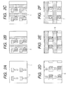
- Figs. 2A, 2B, 2C, 2D, 2E and 2F are schematic plan views showing a fabrication process of the electron source shown in Fig. 1;
- Figs. 3A, 3B, 3C, 3D and 3E are diagrams illustrating an advantage of the present invention in detail
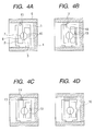
- Figs. 4A, 4B, 4C and 4D are schematic diagrams showing a concrete example of high temperature areas according to the present invention.
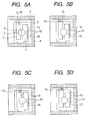
- Figs. 5A, 5B, 5C and 5D are schematic diagrams showing a concrete example of the high temperature areas according to the present invention.
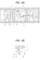
- Figs. 6A and 6B are schematic diagrams showing a preferred configuration example of the high temperature areas according to the present invention.
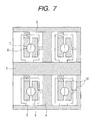
- Fig. 7 is a schematic plan view of an electron source produced in a second example of the present invention.
- Figs. 8A and 8B are schematic plan views of an electron source according to a conventional example.
- Fig. 1 shows a preferred form of an electron source according to the present invention, where reference numeral 1 denotes a glass substrate (PD200 manufactured by Asahi Glass Co., Ltd.: soda lime glass, quartz, etc.) or an electron source substrate consisting of a ceramic substrate.
- the electron source substrate 1 is sometimes coated with silica serving as an alkali block layer to prevent impact on electron source characteristics.
- Reference numerals 2 and 3 respectively denote a scan-side device electrode and signal-side device electrode made of metal film such as Pt, Au, or Ru.
- Reference numeral 7 denotes a conductive film including an electron emitting area 8.
- the conductive film 7 is made of a metal such as Pd or Ru or its oxide.
- the signal-side device electrode 3 is electrically connected with signal wiring 4 which transmits a display signal waveform from an external driver (not shown) to the device.
- the scan-side device electrode 2 is electrically connected with scan wiring 6 which transmits a scan signal waveform from an external driver (not shown) to the device.
- the signal wiring 4 and scan wiring 6, which should have low resistance from the viewpoint of display quality and power consumption, are produced by thick-film printing (screen printing or offset printing), photo printing using photosensitive printing paste, gold-plating or the like.
- Preferable wiring materials include Ag and Cu.
- An electrically insulating layer or high-resistance layer should be provided between the signal wiring 4 and scan wiring 6.
- An insulating layer 5 is provided in Fig. 1.
- the insulating layer 5 can be produced mainly from PbO using thick-film printing or printing by means of photo paste.
- FIG. 1 A fabrication process of the electron source in Fig. 1 is shown in Figs. 2A to 2F.
- the scan-side device electrode 2 is created on the electron source substrate 1 by a thin-film process (Fig. 2A) and the signal-side device electrode 3 is created in a similar manner (Fig. 2B).
- the scan-side device electrode 2 and signal-side device electrode 3 are formed by spattering, vacuum deposition, plasma CVD or other process.
- the signal wiring 4 is created by a thick-film printing process such as screen printing, or photo paste printing by the use of photosensitive material.
- the material used is Ag mixed with glass content.
- a pattern of the insulating layer 5 is formed by photo paste printing (Fig. 2D).
- the insulating layer 5, which requires patterning accuracy, is created by application, exposure, drying, developing and baking from photo paste prepared by mixing a photosensitive material and glass content. Subsequently, the scan wiring 6 is created by a thick-film printing process (Fig. 2E) and the conductive film 7 is formed of Pd and the like by inkjet coating (Fig. 2F).
- the energization forming involves passing a current between the device electrodes 2 and 3 from a power supply (not shown) via the scan wiring 6 and signal wiring 4, locally destroying or deforming the conductive film 7 or changing its quality, and thereby forming an area whose structure has been changed.
- the area whose structure has been changed locally is called an electron emitting area 8.
- the device which has undergone energization forming is subjected to a process called an activation process.
- the activation process is the process of introducing an activating gas so as to create a vacuum, for example, on the order of 10 -2 to 10 -3 Pa and applying voltage pulses of a constant peak value repeatedly as is the case of energization forming. This causes carbon and carbon compounds originating from organic substances present in the vacuum to deposit on a conductive thin film, thereby changing a device current If and emission current Ie greatly.
- the activation process is performed by measuring the device current If and emission current Ie and finished when, for example, the emission current Ie is saturated.
- the voltage pulses applied are desirably at a drive voltage. This enables electron emission through nanogaps, and the electron source is completed.
- the electron source is joined hermetically with a face plate on which a light emitting member such as a phosphor and aluminum metal back is placed as well as with a supporting frame and the like, and the inside is evacuated to produce an image display apparatus.
- a light emitting member such as a phosphor and aluminum metal back
- Vacuum discharges can occur in an image display apparatus because a high voltage on the order of kV to tens of kV is applied to a light emitting member (anode) which emits light in response to electron beams emitted from electron-emitting devices. Although the cause of the discharges remains to be explained definitely, current flow produced by the discharges can often damage the electron-emitting devices as shown in Fig. 3A. Discharge damage leaves traces of cathode spots 10 on the conductive film 7 and device electrodes 2 and 3. Electrode material allegedly melts and evaporates at the cathode spots 10, and a current 11 flows from the anode (not shown) into the cathode spots 10.
- Fig. 3B schematically shows current 12 on device electrodes 2 and 3.
- current concentration, generation of Joule heat, and melting of device electrodes occur at the tips of the cathode spots 10, and consequently the cathode spots advance upstream (to the low-potential side) where electric charges are supplied.
- the current 12 flows from the anode to the device electrodes 2 and 3 through the vacuum and cathode spots 10.
- Joule heat is generated due to current concentration and material begins to melt in suddenly changing portions 13 (those parts at the ends of fusible second areas which are most prone to becoming hot) on the device electrodes 2 and 3.
- new cathode spots 14 are initiated in the suddenly changing portions 13 on the device electrodes 2 and 3 as shown in Fig. 3C.
- a suddenly changing portion is a part where a cross sectional area or resistance for current flow literally changes suddenly.
- the insulating layer 5 which functions as the shielding member has a sufficiently high resistance or consists of an insulating material. Also, the higher the thermal capacity (specific heat x density) and melting point, the better.
- the advantage of the present invention is obtained by providing parts more fusible (second areas) than other parts and exposing them partially, from the insulating layer 5, to connections with wiring.
- the narrow parts of the device electrodes extending from the suddenly changing portions 13 to connections with wiring are second areas, and the other parts of the device electrodes are first areas.
- the fusible second areas reach a high temperature above their melting point when a threshold current flows, shifting the cathode spots to the exposed areas of the second areas. This makes it possible to quench discharges quickly.
- the threshold current is set to discharge current as described above.
- the discharge current depends on the area of the anode, applied voltage, distance between the anode and electron source, anode impedance (described later) etc.
- the anode area is 0.4 m 2
- the applied voltage is 10 kV
- the distance between the anode and electron source is 1.6 mm
- the discharge current is somewhere around 100 amp. depending on the impedance.
- the anode is sometimes divided with the resistance among the divisions increased sufficiently. In that case, the discharge current is reduced to the order of 100/N amp. according to the number N of divisions of the anode.
- the threshold current is set, for example, to a value equal to or lower than allowable current of a driver. Then, even if a single bit fails when a device electrode is broken by a discharge, the driver will remain intact and damage will not spread to a line or block. More preferably, the threshold current is determined by taking into consideration the resistance of the higher resistance wiring, which is assumed here to be a signal wire. When a discharge current flows through the signal wire, a potential rises, causing damage to the electron-emitting devices connected to the signal wire. To avoid this situation, the threshold current is set to Vth/Rsig or below, where Vth is a threshold voltage at which the device is damaged and Rsig is the resistance of the signal wiring to ground.
- the threshold voltage at which the device is damaged is a maximum voltage applied to devices during manufacturing in the case of surface-conduction electron emitters (described later). Specifically, it is a maximum applied voltage in forming, activation or other process (described later).
- hot portions structures of fusible areas (hereinafter sometimes referred to as hot portions) will be described concretely in detail.
- Temperature rises in the suddenly changing portions 13 can be determined from electrical properties (resistance and temperature resistance coefficient) and thermal properties (thermal conductivity, density and specific heat) of wiring material (the device electrodes 2 and 3), thermal properties of the substrate, and geometries of the wiring material and substrate.
- electrical properties resistance and temperature resistance coefficient
- thermal properties thermal conductivity, density and specific heat
- thermal properties of the substrate thermal properties of the substrate
- geometries of the wiring material and substrate For example, a coupled current-field and thermal-conductivity analysis conducted by a finite element solver using shapes and currents as inputs makes it possible to predict that the cathode spots move from 10 to 14 when the temperature reaches the melting point. The new cathode spots 14 are extinguished quickly by shielding effect of the insulating layer 5, making it possible to predict and control the discharge current and its duration.
- Fig. 3E shows an enlarged view of an area near a suddenly changing portion 13 shown in Fig. 3D.
- a configuration may be adopted in which some of them are covered completely with the insulating layer 5 which is a shielding layer.
- a configuration may be adopted in which some of them are covered completely with the insulating layer. That is, according to the present invention, it is sufficient if only part of the fusible areas is exposed from the insulating layer.
- the fusible second areas hot portions are provided as narrow portions with a width of W behind the suddenly changing portions 13 (near the insulating layer 5).
- Fig. 4B shows a structure in which, two suddenly changing portions 13 and 13' are created to initiate a cathode spot 14 more reliably and extinguish an old cathode spot reliably.
- Figs. 4B, 4C and 4D reference numerals of the same components as those in Fig. 4A are omitted.
- a fusible second area is provided by forming a narrow portion in part of the device electrode 2.
- all the two suddenly changing portions 13 and 13' may be covered with the insulating layer 5 which is a shielding layer.
- a high-resistance portion 16 is formed as a fusible hot portion (second area) just below or near the insulating layer 5 on the device electrode 2.
- Possible means of partially increasing resistance include reducing the film thickness partially or making the film porous or coarse.
- the configuration according to the present invention can be achieved easily if a high-resistance material different from the material for the other part is used for the high-resistance portion 16.
- the device electrode 3 in Fig. 4D has a high-resistance portion and narrow portion, and both of them form fusible second areas.
- some of the multiple suddenly changing portions or high-resistance portions are covered with the insulating layer 5, and it is sufficient if only part of them is exposed from the insulating layer as in the case of Fig. 4A.
- hot portions can be provided by lowering the thermal conductivity of the high-resistance portions 16 in Fig. 4D and Figs. 5A to 5D, which in turn can be achieved by decreasing the heat diffusion coefficient, specific heat and density.
- the melting point of the high-resistance portions 16 will be lower than the melting point of the insulating layer 5, it is possible to ensure that extinction of arc will be achieved reliably. This is because if the melting point of the high-resistance portions 16 is higher than that of the insulating layer 5, the insulating layer 5 is likely to melt when the high-resistance portions 16 melts. In that case, the shielding effect of the insulating layer 5 for the cathode spots 14 will be reduced.
- difference in the melting point between the high-resistance portions 16 and insulating layer 5 is 500°C or more.
- the insulating layer 5 must have a sufficient thickness. That is, the use of a material with a high melting point makes it possible to reduce the thickness of the insulating layer 5.
- the insulating layer 5 is made of a material with a high melting point such as SiO 2 , alumina (Al 2 O 3 ) or zirconia (ZrO 2 ).
- the high-resistance portions 16 are made of a material with a low melting point such as lead, zinc, aluminum or ITO containing In.
- Fig. 6B is an enlarged view of that part of the device electrode 2 of the device in the center of Fig. 6A which is located near the region covered with the insulating layer 5.
- the cathode spot 14 advances from the suddenly changing portion 13--which becomes the hottest except for the electron emitting area 8--to the insulating layer 5, and then stagnates at the side of the insulating layer 5 due to electrical shielding effect.
- L denote the distance from the suddenly changing portion 13 to the insulating layer 5
- V gas 2 ⁇ R ⁇ T / M 1 / 2 [where,
- a necessary condition is that arrival time (P/V gas ) determined by the distance P from the cathode spot 14 to the electron emitting area 8 of the adjacent electron-emitting device and the velocity V gas of gas molecules is larger than the time ⁇ until extinction.
- arrival time P/V gas
- the location of the cathode spot 14, which moves to the suddenly changing portion 13 can be substituted with the location of the suddenly changing portion 13.
- 1H f ⁇ N ⁇ 1 sec .
- f is a scroll frequency (Hz)
- N is a scanning frequency (Hz).
- a gas reaching time is shorter than 1H. Accordingly, the above condition would be met if the time ⁇ until extinction is shorter than the gas reaching time.
- P/V gas ⁇ (W + L) /V arc meaning that the distance L from the hot portion to the insulating layer 5 and the electrode width W must satisfy the condition W + L ⁇ P ⁇ V arc /V gas .
- the gas velocity V gas is (2RT/M) 1/2 , where R is a gas constant (8.314772 J/molK).
- R a gas constant (8.314772 J/molK).
- An electron source of the configuration shown in Fig. 1 was constructed using the process shown in Fig. 2.
- An electron source substrate 1 was created by forming a 400-nm silica coat on 2.8-mm thick glass (PD200 manufactured by Asahi Glass Co., Ltd.) by spattering, where the silica coat would serve as an alkali block layer to prevent impact on electron source characteristics.
- PD200 manufactured by Asahi Glass Co., Ltd.
- a Ti film 5 nm in thickness was formed on the electron source substrate 1, a Pt thin-film 20 nm in thickness was formed by spattering, and device electrodes 2 and 3 were formed by patterning through photoresist application, exposure, developing and etching.
- photosensitive printing paste containing Ag was applied by screen printing. This was followed by drying, exposure, developing and baking to create signal wiring 4.
- a photo paste was applied by screen printing, where the photo paste was largely composed of PbO which in turn consisted of glass content and a photosensitive material. This was followed by drying, exposure, developing and baking to create an insulating layer 5.
- the signal wiring 4 was laid in such a way as to cover the insulating layer 5.
- the photo paste containing Ag was applied on top of it by screen printing, followed by drying and baking to create scan wiring 6.
- a conductive film 7 consisting of PdO was created through application by an inkjet process and subsequent baking.
- the distance L from a suddenly changing portion 13 to the insulating layer 5 was 15 ⁇ m
- the covering width W of the device electrodes 2 and 3 in the insulating layer 5 was 20 ⁇ m
- the distance P from the suddenly changing portion 13 to the adjacent electron-emitting device was 175 ⁇ m.
- the electron source was obtained after forming and an activation process. Then, the electron source substrate was bonded by sealing to a face plate equipped with a light emitting member (not shown) and consequently an image display apparatus was constructed. Subsequently, it was electrically connected with a driver (not shown) and high-voltage power supply and an image was displayed by applying a predetermined voltage.
- Figs. 8A and 8B show configurations of the electron source disclosed in Japanese Patent Application Laid-Open No. H09-298030 .
- reference numeral 21 denotes a substrate
- 22 and 23 denote device electrodes
- 24 denotes a conductive film (device film)
- 25 denotes an electron emitting area
- 26 denotes a overcurrent protective film (low melting-point material which functions as a fuse).
- This configuration differs from the above example in that it does not provide an arc extinction structure because only the fuse (low melting-point material) 26 is installed instead of covering hot portions partially with an insulating layer serving as shielding material.
- a cathode spot moves to a fuse when discharging occurs, where the discharge is sustained, and this can cause the gas to fly to an adjacent device to which a voltage is applied, initiating a cycle of discharging and damage in the adjacent device as well. That is, since it is not possible to control locations of fuse blowouts, it may take time before a fuse blowout and a large volume of gas may be generated, causing new discharges in adjacent devices.
- Example 2 differs from example 1 in that high-resistance portions 16 (suddenly changing portion of resistance) are provided, that the high-resistance portions 16 have smaller width, and that ITO is used as material.
- the high-resistance portions 16 tend to be reduced into a material with a lower melting point than the insulating layer 5 which is a covering material.
- the use of low-resistance material for the high-resistance portions 16 makes it possible to maintain the insulating layer 5 which is a covering material in a stable condition and increase the stability of arc extinction.
- ITO layer was formed by spattering and then patterned.
- the rest of the fabrication method was the same as example 1.
- the distance L from the suddenly changing portion 13 of the high-resistance portion 16 which would become hot to the insulating layer 5 was set to 10 ⁇ m
- the covering width W of the device electrodes with the insulating layer was set to 20 ⁇ m
- the distance P to the adjacent electron-emitting device to which a voltage is applied was set to 160 ⁇ m.
- Discharges were generated by increasing the voltages applied to the image display apparatus according to this example and image display apparatus equipped with the electron source according to the conventional example and discharge damage was observed closely. As a result, it was found that the rate at which the discharge damage was confined within a single device was much higher according to this example, thereby confirming the advantage of the present invention.
- hot portions (second areas) in the device electrodes melt and break during discharging, extinguishing the discharges and suppressing new discharges in adjacent electron-emitting devices efficiently. This minimizes the impact of discharging, making it possible to provide highly reliable image display apparatus.
Landscapes
- Cathode-Ray Tubes And Fluorescent Screens For Display (AREA)
- Cold Cathode And The Manufacture (AREA)
Abstract
Description
- The present invention relates to an electron source with an electrode structure which reduces discharges as well as to an image display apparatus which uses the electron source.
- Conventional uses of electron-emitting devices include image display apparatus. For example, an evacuated flat electron beam display panel in which an electron source substrate and counter substrate are placed opposite each other in parallel is known, where the electron source substrate contains a large number of cold-cathode electron-emitting devices and the counter substrate is equipped with an anode electrode which accelerates electrons emitted from the electron-emitting devices and phosphor which acts as a light emitting member. The flat electron beam display panel can have lighter weight and larger screen size than cathode ray tube (CRT) display apparatus widely used today. Also, it can provide brighter, higher-quality images than other flat display panels such as flat liquid crystal display panels, plasma displays, and electroluminescent displays.
- Thus, for image display apparatus which apply voltage between the anode electrode and cold-cathode electron-emitting devices to accelerate the electrons emitted from the cold-cathode electron-emitting devices, it is advantageous to apply a high voltage to maximize emission brightness. Emitted electron beams are dispersed before reaching the anode electrode depending on the type of device, and thus, to implement a high-resolution display, it is preferable to reduce inter-substrate distance between rear plate and face plate.
- However, a higher inter-substrate distance essentially results in a higher electric field between the substrates, making the electron-emitting devices more susceptible to breakage due to discharges.
Japanese Patent Application Laid-Open No. H09-298030 Japanese Patent Application Laid-Open No. H09-245689 Japanese Patent Application Laid-Open No. H07-94076 - However, the techniques disclosed in
Japanese Patent Application Laid-Open No. H09-298030 Japanese Patent Application Laid-Open No. H09-245689 Japanese Patent Application Laid-Open No. H07-94076 - The present invention has an object to solve the above problems, implement an electrode structure which brings about extinction of arc quickly in a reliable manner without maintaining discharge current, and provide an electron source and image display apparatus equipped with the electrode structure.
- According to a first aspect of the present invention, there is provided an electron source comprising:
- a plurality of electron-emitting devices each of which has a pair of device electrodes, and an electron emitting area between the pair of device electrodes;
- first wiring which connects one of the pair of device electrodes of the plurality of electron-emitting devices;
- second wiring which connects the other of the pair of device electrodes of the plurality of electron-emitting devices and intersects the first wiring; and
- an insulating layer which insulates at least an intersection of the first wiring and second wiring and partially covers at least one of the pair of device electrodes,
- wherein the one of the pair of device electrodes has a first area and a second area located between the first area and the first wiring and more fusible than the first area, and the second area is covered partially with the insulating layer.
- According to a second aspect of the present invention, there is provided an image display apparatus comprising the electron source according to the first aspect of the present invention; and an image forming member which has at least a light emitting member for emitting light by irradiation with electrons emitted from the electron source and electrodes used to apply voltage to accelerate the electrons.
- Further features of the present invention will become apparent from the following description of exemplary embodiments (with reference to the attached drawings).
- Fig. 1 is a schematic plan view of a first embodiment of an electron source according to the present invention;
- Figs. 2A, 2B, 2C, 2D, 2E and 2F are schematic plan views showing a fabrication process of the electron source shown in Fig. 1;
- Figs. 3A, 3B, 3C, 3D and 3E are diagrams illustrating an advantage of the present invention in detail;
- Figs. 4A, 4B, 4C and 4D are schematic diagrams showing a concrete example of high temperature areas according to the present invention;
- Figs. 5A, 5B, 5C and 5D are schematic diagrams showing a concrete example of the high temperature areas according to the present invention;
- Figs. 6A and 6B are schematic diagrams showing a preferred configuration example of the high temperature areas according to the present invention;
- Fig. 7 is a schematic plan view of an electron source produced in a second example of the present invention; and
- Figs. 8A and 8B are schematic plan views of an electron source according to a conventional example.
- A preferred embodiment of the present invention will be described with reference to Fig. 1. Fig. 1 shows a preferred form of an electron source according to the present invention, where
reference numeral 1 denotes a glass substrate (PD200 manufactured by Asahi Glass Co., Ltd.: soda lime glass, quartz, etc.) or an electron source substrate consisting of a ceramic substrate. Theelectron source substrate 1 is sometimes coated with silica serving as an alkali block layer to prevent impact on electron source characteristics.Reference numerals Reference numeral 7 denotes a conductive film including anelectron emitting area 8. Theconductive film 7 is made of a metal such as Pd or Ru or its oxide. - The signal-
side device electrode 3 is electrically connected withsignal wiring 4 which transmits a display signal waveform from an external driver (not shown) to the device. The scan-side device electrode 2 is electrically connected withscan wiring 6 which transmits a scan signal waveform from an external driver (not shown) to the device. The signal wiring 4 andscan wiring 6, which should have low resistance from the viewpoint of display quality and power consumption, are produced by thick-film printing (screen printing or offset printing), photo printing using photosensitive printing paste, gold-plating or the like. Preferable wiring materials include Ag and Cu. - An electrically insulating layer or high-resistance layer should be provided between the
signal wiring 4 and scanwiring 6. Aninsulating layer 5 is provided in Fig. 1. The insulatinglayer 5 can be produced mainly from PbO using thick-film printing or printing by means of photo paste. - A fabrication process of the electron source in Fig. 1 is shown in Figs. 2A to 2F.
- The scan-
side device electrode 2 is created on theelectron source substrate 1 by a thin-film process (Fig. 2A) and the signal-side device electrode 3 is created in a similar manner (Fig. 2B). The scan-side device electrode 2 and signal-side device electrode 3 are formed by spattering, vacuum deposition, plasma CVD or other process. Next, as shown in Fig. 2C, thesignal wiring 4 is created by a thick-film printing process such as screen printing, or photo paste printing by the use of photosensitive material. The material used is Ag mixed with glass content. Next, a pattern of the insulatinglayer 5 is formed by photo paste printing (Fig. 2D). The insulatinglayer 5, which requires patterning accuracy, is created by application, exposure, drying, developing and baking from photo paste prepared by mixing a photosensitive material and glass content. Subsequently, thescan wiring 6 is created by a thick-film printing process (Fig. 2E) and theconductive film 7 is formed of Pd and the like by inkjet coating (Fig. 2F). - Next, an electromachining process called energization forming is performed. The energization forming involves passing a current between the
device electrodes scan wiring 6 andsignal wiring 4, locally destroying or deforming theconductive film 7 or changing its quality, and thereby forming an area whose structure has been changed. The area whose structure has been changed locally is called anelectron emitting area 8. - Preferably the device which has undergone energization forming is subjected to a process called an activation process. The activation process is the process of introducing an activating gas so as to create a vacuum, for example, on the order of 10-2 to 10-3 Pa and applying voltage pulses of a constant peak value repeatedly as is the case of energization forming. This causes carbon and carbon compounds originating from organic substances present in the vacuum to deposit on a conductive thin film, thereby changing a device current If and emission current Ie greatly. The activation process is performed by measuring the device current If and emission current Ie and finished when, for example, the emission current Ie is saturated. The voltage pulses applied are desirably at a drive voltage. This enables electron emission through nanogaps, and the electron source is completed.
- The electron source is joined hermetically with a face plate on which a light emitting member such as a phosphor and aluminum metal back is placed as well as with a supporting frame and the like, and the inside is evacuated to produce an image display apparatus.
- An advantage of the present invention will be described concretely with reference to Figs. 3A to 3E.
- Vacuum discharges can occur in an image display apparatus because a high voltage on the order of kV to tens of kV is applied to a light emitting member (anode) which emits light in response to electron beams emitted from electron-emitting devices. Although the cause of the discharges remains to be explained definitely, current flow produced by the discharges can often damage the electron-emitting devices as shown in Fig. 3A. Discharge damage leaves traces of
cathode spots 10 on theconductive film 7 anddevice electrodes - Fig. 3B schematically shows current 12 on
device electrodes device electrodes device electrodes portions 13 on thedevice electrodes - Impedance increases and discharges begin to converge (extinction of arc) at the
old cathode spots 10 due to the cathode spots 14 initiated upstream. On the other hand, the cathode spots 14 initiated in the suddenly changingportions 13 are located near the insulatinglayer 5, and consequently they are shielded by the insulatinglayer 5 and extinguished upon reaching the insulating layer 5 (Fig. 3D). The insulatinglayer 5 which functions as the shielding member has a sufficiently high resistance or consists of an insulating material. Also, the higher the thermal capacity (specific heat x density) and melting point, the better. - Thus, the advantage of the present invention is obtained by providing parts more fusible (second areas) than other parts and exposing them partially, from the insulating
layer 5, to connections with wiring. In the configuration in Fig. 3, the narrow parts of the device electrodes extending from the suddenly changingportions 13 to connections with wiring are second areas, and the other parts of the device electrodes are first areas. In this structure, the fusible second areas reach a high temperature above their melting point when a threshold current flows, shifting the cathode spots to the exposed areas of the second areas. This makes it possible to quench discharges quickly. Preferably the threshold current is set to discharge current as described above. Incidentally, in the case of an image display apparatus, the discharge current depends on the area of the anode, applied voltage, distance between the anode and electron source, anode impedance (described later) etc. For example, if the anode area is 0.4 m2, the applied voltage is 10 kV, and the distance between the anode and electron source is 1.6 mm; then the discharge current is somewhere around 100 amp. depending on the impedance. Also, to reduce the discharge current, the anode is sometimes divided with the resistance among the divisions increased sufficiently. In that case, the discharge current is reduced to the order of 100/N amp. according to the number N of divisions of the anode. Also, desirably the threshold current is set, for example, to a value equal to or lower than allowable current of a driver. Then, even if a single bit fails when a device electrode is broken by a discharge, the driver will remain intact and damage will not spread to a line or block. More preferably, the threshold current is determined by taking into consideration the resistance of the higher resistance wiring, which is assumed here to be a signal wire. When a discharge current flows through the signal wire, a potential rises, causing damage to the electron-emitting devices connected to the signal wire. To avoid this situation, the threshold current is set to Vth/Rsig or below, where Vth is a threshold voltage at which the device is damaged and Rsig is the resistance of the signal wiring to ground. Incidentally, the threshold voltage at which the device is damaged is a maximum voltage applied to devices during manufacturing in the case of surface-conduction electron emitters (described later). Specifically, it is a maximum applied voltage in forming, activation or other process (described later). Next, structures of fusible areas (hereinafter sometimes referred to as hot portions) will be described concretely in detail. - (Suddenly changing structure and thin line structure)
- Temperature rises in the suddenly changing
portions 13 can be determined from electrical properties (resistance and temperature resistance coefficient) and thermal properties (thermal conductivity, density and specific heat) of wiring material (thedevice electrodes 2 and 3), thermal properties of the substrate, and geometries of the wiring material and substrate. For example, a coupled current-field and thermal-conductivity analysis conducted by a finite element solver using shapes and currents as inputs makes it possible to predict that the cathode spots move from 10 to 14 when the temperature reaches the melting point. The new cathode spots 14 are extinguished quickly by shielding effect of the insulatinglayer 5, making it possible to predict and control the discharge current and its duration. To take full advantage of the current-concentrating effect of the suddenly changingportions 13, it is preferable to provide narrow portions with a width of W as fusible hot portions behind the suddenly changing portions 13 (near the insulating layer 5) and set a curvature radius R of the suddenly changing portions to R < (W/5) to (W/10). Fig. 3E shows an enlarged view of an area near a suddenly changingportion 13 shown in Fig. 3D. - When there are two or more suddenly changing
portions 13 --as shown in Fig. 4A-- which become hot and melt when a current above a threshold flows, a configuration may be adopted in which some of them are covered completely with the insulatinglayer 5 which is a shielding layer. Also, when there are two or more fusible areas, a configuration may be adopted in which some of them are covered completely with the insulating layer. That is, according to the present invention, it is sufficient if only part of the fusible areas is exposed from the insulating layer. Again, in the configuration in Fig. 4A, the fusible second areas (hot portions) are provided as narrow portions with a width of W behind the suddenly changing portions 13 (near the insulating layer 5). - Fig. 4B shows a structure in which, two suddenly changing
portions 13 and 13' are created to initiate acathode spot 14 more reliably and extinguish an old cathode spot reliably. Incidentally, in Figs. 4B, 4C and 4D, reference numerals of the same components as those in Fig. 4A are omitted. In Fig. 4B, a fusible second area (hot portion) is provided by forming a narrow portion in part of thedevice electrode 2. Also, as shown in Fig. 4C all the two suddenly changingportions 13 and 13' may be covered with the insulatinglayer 5 which is a shielding layer. - Although various forms of only the
device electrode 2 have been shown above in Figs. 4A to 4C, exactly the same configurations can be used for thedevice electrode 3 without any problem. - (High-resistance structure)
- In Fig. 4D, instead of providing a narrow portion, a high-
resistance portion 16 is formed as a fusible hot portion (second area) just below or near the insulatinglayer 5 on thedevice electrode 2. Possible means of partially increasing resistance include reducing the film thickness partially or making the film porous or coarse. On the other hand, the configuration according to the present invention can be achieved easily if a high-resistance material different from the material for the other part is used for the high-resistance portion 16. Incidentally, thedevice electrode 3 in Fig. 4D has a high-resistance portion and narrow portion, and both of them form fusible second areas. Also, in Figs. 4C and 4D, some of the multiple suddenly changing portions or high-resistance portions are covered with the insulatinglayer 5, and it is sufficient if only part of them is exposed from the insulating layer as in the case of Fig. 4A. - Instead of replacing all the areas containing suddenly changing portions with high-
resistance portions 16 as shown in Fig. 4D, only part of areas containing suddenly changing portions may be replaced with high-resistance portions 16 as shown in Figs. 5A to 5D. Such a structure causes current to flow by avoiding the high-resistance portions 16, and thus current concentration occurs in suddenly changingportions 13, making them hotter than their surroundings. In other words, by inserting high-resistance portions among low-resistance portions, it is possible to provide portions on which current is concentrated and make these portions hotter. Thus, in the configuration in Figs. 5A to 5D, fusible second areas (hot portions) are provided as narrow portions adjacent to the high-resistance portions 16. - (Configuration)
- It is also possible to provide hot portions by varying thermal conductivity, heat diffusion coefficient, specific heat and density instead of electrical characteristics from the surroundings. Specifically, hot portions can be provided by lowering the thermal conductivity of the high-
resistance portions 16 in Fig. 4D and Figs. 5A to 5D, which in turn can be achieved by decreasing the heat diffusion coefficient, specific heat and density. - If materials are selected such that the melting point of the high-
resistance portions 16 will be lower than the melting point of the insulatinglayer 5, it is possible to ensure that extinction of arc will be achieved reliably. This is because if the melting point of the high-resistance portions 16 is higher than that of the insulatinglayer 5, the insulatinglayer 5 is likely to melt when the high-resistance portions 16 melts. In that case, the shielding effect of the insulatinglayer 5 for the cathode spots 14 will be reduced. Preferably, difference in the melting point between the high-resistance portions 16 and insulatinglayer 5 is 500°C or more. - To maintain the shielding effect even when the insulating
layer 5 melts, the insulating layer must have a sufficient thickness. That is, the use of a material with a high melting point makes it possible to reduce the thickness of the insulatinglayer 5. Preferably, the insulatinglayer 5 is made of a material with a high melting point such as SiO2, alumina (Al2O3) or zirconia (ZrO2). - Preferably, the high-
resistance portions 16 are made of a material with a low melting point such as lead, zinc, aluminum or ITO containing In. - (Rules for creepage distance)
- Preferable locations of exposed areas of the high-
resistance portions 16 or suddenly changingportions 13 in Figs. 3 to 5 with respect to the insulatinglayer 5 will be described with reference to Fig. 6. Incidentally, Fig. 6B is an enlarged view of that part of thedevice electrode 2 of the device in the center of Fig. 6A which is located near the region covered with the insulatinglayer 5. - As shown in Fig. 6B, when a current is passed through the wiring, the
cathode spot 14 advances from the suddenly changingportion 13--which becomes the hottest except for theelectron emitting area 8--to the insulatinglayer 5, and then stagnates at the side of the insulatinglayer 5 due to electrical shielding effect. Let L denote the distance from the suddenly changingportion 13 to the insulatinglayer 5 and let W denote the width (covering width of device electrode with the insulating layer) of an exposed area of a hot portion (fusible second area) at a boundary between the exposed area and insulating layer. It can be seen that until extinction, thecathode spot 14 advances to a distance of (W + L) at the most from the suddenly changingportion 13 which becomes the hottest. If the time until extinction is τ and the rate of advance of thecathode spot 14 is Varc (= 200 m/s), then it can be estimated that τ = (W + L)/Varc. - On the other hand, gas generated from the
cathode spot 14 diffuses to surrounding areas at a velocity Vgas given by the equation below and reaches an adjacent electron-emitting device. If gas partial pressure rises there, the adjacent electron-emitting device may discharge.
[where, - R: gas constant = 8.314772 J/molK
- T: melting point of the electrode (Pt, according to the present invention) = 2042.15K
- M: mass numbers of spouting gases (Ar and Pt, according to the present invention; 39.948g/mol which is the mass number of Ar is adopted)]
- In this case, the given electron-emitting device and the adjacent electron-emitting device are damaged in succession, resulting in marked defects. To avoid this situation, a necessary condition is that arrival time (P/Vgas) determined by the distance P from the
cathode spot 14 to theelectron emitting area 8 of the adjacent electron-emitting device and the velocity Vgas of gas molecules is larger than the time τ until extinction. Incidentally, the location of thecathode spot 14, which moves to the suddenly changingportion 13, can be substituted with the location of the suddenly changingportion 13. - It is an important condition that the time τ until extinction is shorter than a time period 1H of selecting scan wiring. 1H is defined as follow:

Wherein, f is a scroll frequency (Hz), and N is a scanning frequency (Hz).
In general, a gas reaching time is shorter than 1H. Accordingly, the above condition would be met if the time τ until extinction is shorter than the gas reaching time. - That is, P/Vgas ≥ (W + L) /Varc, meaning that the distance L from the hot portion to the insulating
layer 5 and the electrode width W must satisfy the condition W + L ≤ P·Varc/Vgas . - Generally, the velocity Varc of a cathode spot is reported to range from 10 to 500 m/s (HANDBOOK OF VACUUM ARC SCIENCE AND TECHNOLOGY, NOYES PUBLICATIONS, 1995, pp86). According to the present invention, approximately Varc = 200 m/s. The gas velocity Vgas is (2RT/M) 1/2 , where R is a gas constant (8.314772 J/molK). According to the present invention, platinum electrode material and gases such as Ar taken in during deposition of the platinum electrode material are predominant, and thus T is between the melting point and boiling point of platinum (2,042 to 4,100 K) and M = 39.95. It follows that the gas velocity Vgas is approximately 1000 m/s. Therefore, the distance (W + L) ≤ P/5. More particularly, for a high-definition image display apparatus, approximately P = 200 µm. Thus, W + L ≤ 40 µm is a necessary condition.
- (Examples)
- (Example 1)
- An electron source of the configuration shown in Fig. 1 was constructed using the process shown in Fig. 2.
- An
electron source substrate 1 was created by forming a 400-nm silica coat on 2.8-mm thick glass (PD200 manufactured by Asahi Glass Co., Ltd.) by spattering, where the silica coat would serve as an alkali block layer to prevent impact on electron source characteristics. - A
Ti film 5 nm in thickness was formed on theelectron source substrate 1, a Pt thin-film 20 nm in thickness was formed by spattering, anddevice electrodes - Then, photosensitive printing paste containing Ag was applied by screen printing. This was followed by drying, exposure, developing and baking to create
signal wiring 4. Next, to obtain high positional accuracy, a photo paste was applied by screen printing, where the photo paste was largely composed of PbO which in turn consisted of glass content and a photosensitive material. This was followed by drying, exposure, developing and baking to create aninsulating layer 5. As shown in Fig. 1, thesignal wiring 4 was laid in such a way as to cover the insulatinglayer 5. The photo paste containing Ag was applied on top of it by screen printing, followed by drying and baking to createscan wiring 6. - After cleaning the substrate, a
conductive film 7 consisting of PdO was created through application by an inkjet process and subsequent baking. - The distance L from a suddenly changing
portion 13 to the insulatinglayer 5 was 15 µm, the covering width W of thedevice electrodes layer 5 was 20 µm, and the distance P from the suddenly changingportion 13 to the adjacent electron-emitting device (distance P from the suddenly changingportion 13 to the electron emitting area 8) was 175 µm. - Next, the electron source was obtained after forming and an activation process. Then, the electron source substrate was bonded by sealing to a face plate equipped with a light emitting member (not shown) and consequently an image display apparatus was constructed. Subsequently, it was electrically connected with a driver (not shown) and high-voltage power supply and an image was displayed by applying a predetermined voltage.
- Figs. 8A and 8B show configurations of the electron source disclosed in
Japanese Patent Application Laid-Open No. H09-298030 - Even with the image display apparatus according to the present invention, discharges may occur when the voltage applied is increased. When discharge damage was closely observed, it was found that the rate at which the discharge damage was confined within a single device was far higher than that of the conventional example, thereby confirming the advantage of the present invention.
- Also, as a comparative example, an image display apparatus was constructed and examined, where the distance L from the suddenly changing
portion 13 in Fig. 1 to the insulating layer was set to 20 µm, the covering width W of the device electrodes with the insulating layer was set between 50 and 10 µm, and the distance P to the adjacent electron-emitting device to which a voltage is applied (distance P from the suddenly changingportion 13 to the electron emitting area 8) was set to 175 µm. As a result, it was found that the rate at which the discharge damage was confined within a single device according to the present invention was higher than any of the comparative examples. - (Example 2)
- An electron source of the configuration shown in Fig. 7 was constructed.
- Example 2 differs from example 1 in that high-resistance portions 16 (suddenly changing portion of resistance) are provided, that the high-
resistance portions 16 have smaller width, and that ITO is used as material. Thus, when cathode spots are initiated, the high-resistance portions 16 tend to be reduced into a material with a lower melting point than the insulatinglayer 5 which is a covering material. The use of low-resistance material for the high-resistance portions 16 makes it possible to maintain the insulatinglayer 5 which is a covering material in a stable condition and increase the stability of arc extinction. - An ITO layer was formed by spattering and then patterned. The rest of the fabrication method was the same as example 1.
- In this example, the distance L from the suddenly changing
portion 13 of the high-resistance portion 16 which would become hot to the insulatinglayer 5 was set to 10 µm, the covering width W of the device electrodes with the insulating layer was set to 20 µm, and the distance P to the adjacent electron-emitting device to which a voltage is applied (distance P from the suddenly changingportion 13 to the electron emitting area 8) was set to 160 µm. - Discharges were generated by increasing the voltages applied to the image display apparatus according to this example and image display apparatus equipped with the electron source according to the conventional example and discharge damage was observed closely. As a result, it was found that the rate at which the discharge damage was confined within a single device was much higher according to this example, thereby confirming the advantage of the present invention.
- According to the present invention, hot portions (second areas) in the device electrodes melt and break during discharging, extinguishing the discharges and suppressing new discharges in adjacent electron-emitting devices efficiently. This minimizes the impact of discharging, making it possible to provide highly reliable image display apparatus.
- While the present invention has been described with reference to exemplary embodiments, it is to be understood that the invention is not limited to the disclosed exemplary embodiments. The scope of the following claims is to be accorded the broadest interpretation so as to encompass all such modifications and equivalent structures and functions. To implement an electrode structure which brings about extinction of arc quickly in a reliable manner without maintaining discharge current, and provide an electron source and image display apparatus equipped with the electrode structure.
Device electrodes wiring 6 andsignal wiring 4, and an insulatinglayer 5 which insulates thescan wiring 6 andsignal wiring 4 are extended to cover the narrow portions of thedevice electrodes
Claims (8)
- An electron source comprising:a plurality of electron-emitting devices each of which has a pair of device electrodes and an electron emitting area between the pair of device electrodes;first wiring which connects one of the pair of device electrodes of the plurality of electron-emitting devices;second wiring which connects the other of the pair of device electrodes of the plurality of electron-emitting devices and intersects the first wiring; andan insulating layer which insulates at least an intersection of the first wiring and second wiring and partially covers at least one of the pair of device electrodes,wherein the one of the pair of device electrodes has a first area and a second area located between the first area and the first wiring and more fusible than the first wiring, and the second area is partially exposed and covered with the insulating layer.
- The electron source according to claim 1, wherein the following relationship is satisfied:

where L is distance from an exposed area of the second area to the insulating layer, W is width of the exposed area at a boundary between the exposed area and the insulating layer, and P is distance from the exposed area to an adjacent electron-emitting device. - The electron source according to claim 1, wherein width of the second area is smaller than width of the first area.
- The electron source according to claim 1, wherein thickness of the second area is smaller than thickness of the first area.
- The electron source according to claim 1, wherein resistance of the second area is higher than resistance of the first area.
- The electron source according to claim 5, wherein the second area is made of a higher-resistance material than the first area.
- The electron source according to claim 1, wherein the second area is made of a material with a smaller heat diffusion coefficient than the first area.
- An image display apparatus comprising:the electron source according to claim 1 ; and an image forming member which has at least a light emitting member for emitting light by irradiation with electrons emitted from the electron source and electrodes used to apply voltage to accelerate the electrons.
Applications Claiming Priority (2)
| Application Number | Priority Date | Filing Date | Title |
|---|---|---|---|
| JP2005241944 | 2005-08-24 | ||
| JP2006215176A JP2007087934A (en) | 2005-08-24 | 2006-08-08 | Electron source and image display device |
Publications (3)
| Publication Number | Publication Date |
|---|---|
| EP1758146A2 true EP1758146A2 (en) | 2007-02-28 |
| EP1758146A3 EP1758146A3 (en) | 2008-09-03 |
| EP1758146B1 EP1758146B1 (en) | 2010-04-07 |
Family
ID=37507646
Family Applications (1)
| Application Number | Title | Priority Date | Filing Date |
|---|---|---|---|
| EP06119387A Not-in-force EP1758146B1 (en) | 2005-08-24 | 2006-08-23 | Electron source and image display apparatus |
Country Status (5)
| Country | Link |
|---|---|
| US (1) | US7382088B2 (en) |
| EP (1) | EP1758146B1 (en) |
| JP (1) | JP2007087934A (en) |
| CN (1) | CN1921051B (en) |
| DE (1) | DE602006013380D1 (en) |
Cited By (2)
| Publication number | Priority date | Publication date | Assignee | Title |
|---|---|---|---|---|
| EP2023369A3 (en) * | 2007-08-09 | 2010-03-31 | Canon Kabushiki Kaisha | Electron-emitting device and image display apparatus |
| EP2413344A1 (en) * | 2010-07-26 | 2012-02-01 | Canon Kabushiki Kaisha | Image display apparatus |
Families Citing this family (17)
| Publication number | Priority date | Publication date | Assignee | Title |
|---|---|---|---|---|
| US7427826B2 (en) * | 2005-01-25 | 2008-09-23 | Canon Kabushiki Kaisha | Electron beam apparatus |
| JP2008066280A (en) * | 2006-08-08 | 2008-03-21 | Canon Inc | Image display device |
| JP2008257913A (en) * | 2007-04-02 | 2008-10-23 | Canon Inc | Electron beam equipment |
| JP2008257912A (en) * | 2007-04-02 | 2008-10-23 | Canon Inc | Electron beam equipment |
| JP2008309939A (en) * | 2007-06-13 | 2008-12-25 | Canon Inc | Electron source and image display device |
| US7972461B2 (en) * | 2007-06-27 | 2011-07-05 | Canon Kabushiki Kaisha | Hermetically sealed container and manufacturing method of image forming apparatus using the same |
| JP2009059547A (en) * | 2007-08-31 | 2009-03-19 | Canon Inc | Electron emitting device and manufacturing method thereof |
| JP2009076240A (en) * | 2007-09-19 | 2009-04-09 | Canon Inc | Electron emission device and image display device using the same |
| JP2010021065A (en) * | 2008-07-11 | 2010-01-28 | Canon Inc | Electron source, and image display apparatus |
| JP2010067398A (en) * | 2008-09-09 | 2010-03-25 | Canon Inc | Electron beam apparatus |
| JP2010140739A (en) * | 2008-12-11 | 2010-06-24 | Canon Inc | Electron-source substrate, and image display apparatus |
| JP2010244830A (en) * | 2009-04-06 | 2010-10-28 | Canon Inc | Image display device and manufacturing method thereof |
| JP2010262892A (en) * | 2009-05-11 | 2010-11-18 | Canon Inc | Electron beam apparatus and image display apparatus using the same |
| JP2010267474A (en) * | 2009-05-14 | 2010-11-25 | Canon Inc | Electron beam apparatus and image display apparatus using the same |
| JP2011018491A (en) * | 2009-07-08 | 2011-01-27 | Canon Inc | Electron emitting device, electron beam apparatus using this, and image display apparatus |
| JP5351860B2 (en) | 2009-09-04 | 2013-11-27 | 乾坤科技股▲ふん▼有限公司 | Protective device |
| US9025295B2 (en) | 2009-09-04 | 2015-05-05 | Cyntec Co., Ltd. | Protective device and protective module |
Citations (1)
| Publication number | Priority date | Publication date | Assignee | Title |
|---|---|---|---|---|
| US20050082963A1 (en) | 1999-03-05 | 2005-04-21 | Canon Kabushiki Kaisha | Image formation apparatus |
Family Cites Families (22)
| Publication number | Priority date | Publication date | Assignee | Title |
|---|---|---|---|---|
| US6313815B1 (en) * | 1991-06-06 | 2001-11-06 | Canon Kabushiki Kaisha | Electron source and production thereof and image-forming apparatus and production thereof |
| US5763997A (en) * | 1992-03-16 | 1998-06-09 | Si Diamond Technology, Inc. | Field emission display device |
| JP3167072B2 (en) * | 1992-12-29 | 2001-05-14 | キヤノン株式会社 | Image forming device |
| JP2699827B2 (en) | 1993-09-27 | 1998-01-19 | 双葉電子工業株式会社 | Field emission cathode device |
| US5594296A (en) * | 1993-12-27 | 1997-01-14 | Canon Kabushiki Kaisha | Electron source and electron beam apparatus |
| US6246168B1 (en) * | 1994-08-29 | 2001-06-12 | Canon Kabushiki Kaisha | Electron-emitting device, electron source and image-forming apparatus as well as method of manufacturing the same |
| US5578896A (en) * | 1995-04-10 | 1996-11-26 | Industrial Technology Research Institute | Cold cathode field emission display and method for forming it |
| JPH08329826A (en) * | 1995-05-30 | 1996-12-13 | Canon Inc | Electron source and image forming apparatus |
| JPH09245689A (en) | 1996-03-13 | 1997-09-19 | Toshiba Corp | Image display device using field emission cold cathode |
| JPH09298030A (en) | 1996-04-30 | 1997-11-18 | Canon Inc | Electron emitting device, electron source, and image forming apparatus |
| US6396207B1 (en) * | 1998-10-20 | 2002-05-28 | Canon Kabushiki Kaisha | Image display apparatus and method for producing the same |
| US6537427B1 (en) * | 1999-02-04 | 2003-03-25 | Micron Technology, Inc. | Deposition of smooth aluminum films |
| EP1077443A4 (en) * | 1999-03-05 | 2004-06-16 | Canon Kk | Image forming device |
| JP3768803B2 (en) | 2000-11-09 | 2006-04-19 | キヤノン株式会社 | Image display device |
| KR100413815B1 (en) * | 2002-01-22 | 2004-01-03 | 삼성에스디아이 주식회사 | Carbon nano tube field emitter device in triode structure and its fabricating method |
| JP3848228B2 (en) * | 2002-09-06 | 2006-11-22 | キヤノン株式会社 | Wiring device manufacturing method, electron source substrate manufacturing method, and image display device manufacturing method |
| JP4366920B2 (en) * | 2002-11-07 | 2009-11-18 | ソニー株式会社 | Flat display device and manufacturing method thereof |
| CN100419939C (en) | 2003-01-21 | 2008-09-17 | 佳能株式会社 | Energized processing method and mfg. method of electronic source substrate |
| JP4579630B2 (en) | 2004-09-22 | 2010-11-10 | キヤノン株式会社 | Electron beam apparatus manufacturing method and electron beam apparatus |
| JP4886184B2 (en) | 2004-10-26 | 2012-02-29 | キヤノン株式会社 | Image display device |
| JP4817641B2 (en) | 2004-10-26 | 2011-11-16 | キヤノン株式会社 | Image forming apparatus |
| US7427826B2 (en) | 2005-01-25 | 2008-09-23 | Canon Kabushiki Kaisha | Electron beam apparatus |
-
2006
- 2006-08-08 JP JP2006215176A patent/JP2007087934A/en not_active Withdrawn
- 2006-08-11 US US11/464,098 patent/US7382088B2/en not_active Expired - Fee Related
- 2006-08-23 EP EP06119387A patent/EP1758146B1/en not_active Not-in-force
- 2006-08-23 DE DE602006013380T patent/DE602006013380D1/en active Active
- 2006-08-24 CN CN2006101150942A patent/CN1921051B/en not_active Expired - Fee Related
Patent Citations (1)
| Publication number | Priority date | Publication date | Assignee | Title |
|---|---|---|---|---|
| US20050082963A1 (en) | 1999-03-05 | 2005-04-21 | Canon Kabushiki Kaisha | Image formation apparatus |
Cited By (3)
| Publication number | Priority date | Publication date | Assignee | Title |
|---|---|---|---|---|
| EP2023369A3 (en) * | 2007-08-09 | 2010-03-31 | Canon Kabushiki Kaisha | Electron-emitting device and image display apparatus |
| US7952265B2 (en) | 2007-08-09 | 2011-05-31 | Canon Kabushiki Kaisha | Electron-emitting device and image display apparatus |
| EP2413344A1 (en) * | 2010-07-26 | 2012-02-01 | Canon Kabushiki Kaisha | Image display apparatus |
Also Published As
| Publication number | Publication date |
|---|---|
| US20070046173A1 (en) | 2007-03-01 |
| US7382088B2 (en) | 2008-06-03 |
| DE602006013380D1 (en) | 2010-05-20 |
| JP2007087934A (en) | 2007-04-05 |
| EP1758146A3 (en) | 2008-09-03 |
| EP1758146B1 (en) | 2010-04-07 |
| CN1921051B (en) | 2010-06-02 |
| CN1921051A (en) | 2007-02-28 |
Similar Documents
| Publication | Publication Date | Title |
|---|---|---|
| EP1758146B1 (en) | Electron source and image display apparatus | |
| US7427826B2 (en) | Electron beam apparatus | |
| US7795795B2 (en) | Electron beam apparatus having an electrode with high temperature portion | |
| US7710010B2 (en) | Electron beam apparatus | |
| US6963159B2 (en) | Image-forming apparatus and spacer | |
| US7211943B2 (en) | Electron source plate, image-forming apparatus using the same, and fabricating method thereof | |
| US7458872B2 (en) | Method of manufacturing electron-emitting device, electron source, and image display device | |
| US7195533B2 (en) | Method for fabricating envelope and method for fabricating image display apparatus | |
| JP2003157757A (en) | Electron source substrate and display device using the same | |
| JPH0765708A (en) | Method for manufacturing electron-emitting device and image forming apparatus | |
| JP2003151475A (en) | Electron source substrate, manufacturing method thereof, and image forming apparatus using electron source substrate | |
| JP4522275B2 (en) | Electron beam apparatus and display panel using the same | |
| US7482742B2 (en) | Electron source substrate with high-impedance portion, and image-forming apparatus | |
| JP2005259552A (en) | Manufacturing method of electron source and manufacturing method of image display device | |
| JP4228853B2 (en) | Spacer inspection method and display device manufacturing method | |
| JP2004055347A (en) | Electron-emitting device, electron-emitting device, display device, and method of manufacturing electron-emitting device | |
| US20100148670A1 (en) | Electron source substrate and image display apparatus | |
| JP2000244079A (en) | Matrix wiring board, electron source board and image forming apparatus | |
| US20100007584A1 (en) | Electron source and image display apparatus | |
| JP2004342546A (en) | Method of manufacturing electron source and method of manufacturing image display device | |
| JP2005222931A (en) | Electron emitting device, electron source, and manufacturing method of image display device | |
| JP2006210091A (en) | Electron source, electron source manufacturing method, electro-optical device, and electronic apparatus | |
| JP2004071370A (en) | Wiring board, electron source board and image forming apparatus | |
| JP2004362904A (en) | Wiring board, image forming apparatus, and manufacturing method of wiring board | |
| JP2006172855A (en) | Electron emitting device, electron emitting device manufacturing method, electro-optical device, and electronic apparatus |
Legal Events
| Date | Code | Title | Description |
|---|---|---|---|
| PUAI | Public reference made under article 153(3) epc to a published international application that has entered the european phase |
Free format text: ORIGINAL CODE: 0009012 |
|
| AK | Designated contracting states |
Kind code of ref document: A2 Designated state(s): AT BE BG CH CY CZ DE DK EE ES FI FR GB GR HU IE IS IT LI LT LU LV MC NL PL PT RO SE SI SK TR |
|
| AX | Request for extension of the european patent |
Extension state: AL BA HR MK YU |
|
| PUAL | Search report despatched |
Free format text: ORIGINAL CODE: 0009013 |
|
| AK | Designated contracting states |
Kind code of ref document: A3 Designated state(s): AT BE BG CH CY CZ DE DK EE ES FI FR GB GR HU IE IS IT LI LT LU LV MC NL PL PT RO SE SI SK TR |
|
| AX | Request for extension of the european patent |
Extension state: AL BA HR MK RS |
|
| RIC1 | Information provided on ipc code assigned before grant |
Ipc: H01J 1/316 20060101AFI20080729BHEP |
|
| 17P | Request for examination filed |
Effective date: 20090303 |
|
| AKX | Designation fees paid |
Designated state(s): DE FR GB IT NL |
|
| GRAP | Despatch of communication of intention to grant a patent |
Free format text: ORIGINAL CODE: EPIDOSNIGR1 |
|
| RIC1 | Information provided on ipc code assigned before grant |
Ipc: H01J 31/12 20060101ALI20090909BHEP Ipc: H01J 29/04 20060101ALI20090909BHEP Ipc: H01J 1/316 20060101AFI20090909BHEP |
|
| GRAS | Grant fee paid |
Free format text: ORIGINAL CODE: EPIDOSNIGR3 |
|
| GRAA | (expected) grant |
Free format text: ORIGINAL CODE: 0009210 |
|
| AK | Designated contracting states |
Kind code of ref document: B1 Designated state(s): DE FR GB IT NL |
|
| REG | Reference to a national code |
Ref country code: GB Ref legal event code: FG4D |
|
| REF | Corresponds to: |
Ref document number: 602006013380 Country of ref document: DE Date of ref document: 20100520 Kind code of ref document: P |
|
| REG | Reference to a national code |
Ref country code: NL Ref legal event code: VDEP Effective date: 20100407 |
|
| PG25 | Lapsed in a contracting state [announced via postgrant information from national office to epo] |
Ref country code: NL Free format text: LAPSE BECAUSE OF FAILURE TO SUBMIT A TRANSLATION OF THE DESCRIPTION OR TO PAY THE FEE WITHIN THE PRESCRIBED TIME-LIMIT Effective date: 20100407 |
|
| PLBE | No opposition filed within time limit |
Free format text: ORIGINAL CODE: 0009261 |
|
| STAA | Information on the status of an ep patent application or granted ep patent |
Free format text: STATUS: NO OPPOSITION FILED WITHIN TIME LIMIT |
|
| 26N | No opposition filed |
Effective date: 20110110 |
|
| PG25 | Lapsed in a contracting state [announced via postgrant information from national office to epo] |
Ref country code: IT Free format text: LAPSE BECAUSE OF FAILURE TO SUBMIT A TRANSLATION OF THE DESCRIPTION OR TO PAY THE FEE WITHIN THE PRESCRIBED TIME-LIMIT Effective date: 20100407 |
|
| REG | Reference to a national code |
Ref country code: FR Ref legal event code: ST Effective date: 20110502 |
|
| PG25 | Lapsed in a contracting state [announced via postgrant information from national office to epo] |
Ref country code: FR Free format text: LAPSE BECAUSE OF NON-PAYMENT OF DUE FEES Effective date: 20100831 |
|
| PGFP | Annual fee paid to national office [announced via postgrant information from national office to epo] |
Ref country code: DE Payment date: 20130831 Year of fee payment: 8 |
|
| PGFP | Annual fee paid to national office [announced via postgrant information from national office to epo] |
Ref country code: GB Payment date: 20130822 Year of fee payment: 8 |
|
| REG | Reference to a national code |
Ref country code: DE Ref legal event code: R119 Ref document number: 602006013380 Country of ref document: DE |
|
| GBPC | Gb: european patent ceased through non-payment of renewal fee |
Effective date: 20140823 |
|
| REG | Reference to a national code |
Ref country code: DE Ref legal event code: R119 Ref document number: 602006013380 Country of ref document: DE Effective date: 20150303 |
|
| PG25 | Lapsed in a contracting state [announced via postgrant information from national office to epo] |
Ref country code: DE Free format text: LAPSE BECAUSE OF NON-PAYMENT OF DUE FEES Effective date: 20150303 Ref country code: GB Free format text: LAPSE BECAUSE OF NON-PAYMENT OF DUE FEES Effective date: 20140823 |