EP1755179A2 - Electroluminescent device - Google Patents
Electroluminescent device Download PDFInfo
- Publication number
- EP1755179A2 EP1755179A2 EP05027949A EP05027949A EP1755179A2 EP 1755179 A2 EP1755179 A2 EP 1755179A2 EP 05027949 A EP05027949 A EP 05027949A EP 05027949 A EP05027949 A EP 05027949A EP 1755179 A2 EP1755179 A2 EP 1755179A2
- Authority
- EP
- European Patent Office
- Prior art keywords
- current
- light
- polarizer
- color
- magnitude
- Prior art date
- Legal status (The legal status is an assumption and is not a legal conclusion. Google has not performed a legal analysis and makes no representation as to the accuracy of the status listed.)
- Granted
Links
Images
Classifications
-
- H—ELECTRICITY
- H05—ELECTRIC TECHNIQUES NOT OTHERWISE PROVIDED FOR
- H05B—ELECTRIC HEATING; ELECTRIC LIGHT SOURCES NOT OTHERWISE PROVIDED FOR; CIRCUIT ARRANGEMENTS FOR ELECTRIC LIGHT SOURCES, IN GENERAL
- H05B33/00—Electroluminescent light sources
- H05B33/12—Light sources with substantially two-dimensional [2D] radiating surfaces
- H05B33/22—Light sources with substantially two-dimensional [2D] radiating surfaces characterised by the chemical or physical composition or the arrangement of auxiliary dielectric or reflective layers
-
- H—ELECTRICITY
- H10—SEMICONDUCTOR DEVICES; ELECTRIC SOLID-STATE DEVICES NOT OTHERWISE PROVIDED FOR
- H10K—ORGANIC ELECTRIC SOLID-STATE DEVICES
- H10K59/00—Integrated devices, or assemblies of multiple devices, comprising at least one organic light-emitting element covered by group H10K50/00
- H10K59/80—Constructional details
- H10K59/8791—Arrangements for improving contrast, e.g. preventing reflection of ambient light
-
- H—ELECTRICITY
- H10—SEMICONDUCTOR DEVICES; ELECTRIC SOLID-STATE DEVICES NOT OTHERWISE PROVIDED FOR
- H10K—ORGANIC ELECTRIC SOLID-STATE DEVICES
- H10K50/00—Organic light-emitting devices
- H10K50/80—Constructional details
- H10K50/86—Arrangements for improving contrast, e.g. preventing reflection of ambient light
-
- H—ELECTRICITY
- H10—SEMICONDUCTOR DEVICES; ELECTRIC SOLID-STATE DEVICES NOT OTHERWISE PROVIDED FOR
- H10K—ORGANIC ELECTRIC SOLID-STATE DEVICES
- H10K59/00—Integrated devices, or assemblies of multiple devices, comprising at least one organic light-emitting element covered by group H10K50/00
- H10K59/30—Devices specially adapted for multicolour light emission
- H10K59/35—Devices specially adapted for multicolour light emission comprising red-green-blue [RGB] subpixels
-
- Y—GENERAL TAGGING OF NEW TECHNOLOGICAL DEVELOPMENTS; GENERAL TAGGING OF CROSS-SECTIONAL TECHNOLOGIES SPANNING OVER SEVERAL SECTIONS OF THE IPC; TECHNICAL SUBJECTS COVERED BY FORMER USPC CROSS-REFERENCE ART COLLECTIONS [XRACs] AND DIGESTS
- Y10—TECHNICAL SUBJECTS COVERED BY FORMER USPC
- Y10S—TECHNICAL SUBJECTS COVERED BY FORMER USPC CROSS-REFERENCE ART COLLECTIONS [XRACs] AND DIGESTS
- Y10S428/00—Stock material or miscellaneous articles
- Y10S428/917—Electroluminescent
Definitions
- the invention relates to a display device, and more particularly, an organic electroluminescent device.
- the brightness characteristics of the red pixels R are typically inferior to those of the green G and blue B pixels.
- more current should be applied the R pixels in order to emit the same level of brightness as the G and B pixels.
- 10mA current should be applied to the G pixel
- 20mA current should be applied to the B pixel.
- a 70mA current should be applied to the R pixel in order to emit 100 cadela of brightness.
- a great deal of current is required to emit the same level of brightness from the R, G and B pixels, thereby increasing the power consumption of the organic electroluminescent device. Therefore, there is a need to decrease power consumption requirements of organic electroluminescent devices while maintaining desired display characteristics
- An object of the invention is to solve at least the above problems and/or disadvantages and to provide at least the advantages described hereinafter.
- Another object is to decrease total current required when the organic electroluminescent device emits.
- Another object of the invention is to provide an organic electroluminescent device which decreases current required at the time of emitting of the organic electroluminescent device by using a colored polarizer according to brightness characteristics of R, G and B pixels.
- an organic electroluminescent device in accordance with an embodiment of the invention includes a substrate, an anode electrode layer, an organic layer, a cathode electrode layer and a colored polarizer, the colored polarizer polarizing light incident from the outside being adhered to a surface of the substrate contrary to an upper side of the substrate on which the anode electrode layer is formed.
- the organic electroluminescent device in accordance with embodiments of the present invention may minimize power consumption by decreasing total current required when the organic electroluminescent device emits.
- the organic electroluminescent device in accordance with embodiments of the invention uses a colored polarizer according to brightness characteristics of R, G and B pixels, thereby decreasing current required when the organic electroluminescent device emits.
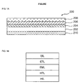
- the organic electroluminescent device 200 shown in FIG. 1A includes a substrate 202, an anode electrode layer 204, an organic layer 206, a cathode electrode layer 208 and a colored polarizer 210.
- the anode electrode layer 204 may be provided on the substrate 202 by, for example, a deposition type process.
- the organic layer 206 may be provided on the anode electrode layer 204 by, for example, a deposition type process, and may include a hole injection layer (HIL), a hole transporting layer (HTL), an emitting layer (EML), an electron transporting layer (ETL), and an electron injection layer (EIL), as shown in FIG. 1 B. These layers of the organic layer 206 may be formed in the sequence shown in FIG. 1B, however, other arrangements may also be appropriate.
- the cathode electrode layer 208 may be formed from a metal such as, for example, aluminum (AI), and may be provided on the organic layer 206 by, for example, a deposition type process.
- AI aluminum
- the anode electrode layer 204 provides holes to the HIL of the organic emitting layer 206 if a certain positive voltage is applied thereto.
- the cathode electrode layer 208 provides electrons to the EIL of the organic emitting layer 206 if a certain negative voltage is applied thereto.
- the HIL smoothly injects the holes provided from the anode electrode layer 204 to the HTL, and the EIL smoothly injects the electrons provided from the cathode electrode layer 208 to the ETL.
- the HTL then transports the holes received from the HIL into the EML, and the ETL transports the electrons received from the EIL into the EML.
- the transported holes and electrons are recombined in the EML, and a light having a predetermined wavelength is from the EML of the organic emitting layer 206 to the outside through the substrate 202 and the polarizer 210.
- the polarizer 210 may be provided on a surface of the substrate 202 which is opposite an upper surface of the substrate 202 on which the anode electrode layer 204 is provided, that is, a lower surface of the substrate 202, as shown in FIG. 1A. However, other positions for the polarizer 210 may also be appropriate. For example, the polarizer 210 may be provided between the substrate 202 and the anode electrode layer 204. The polarizer 210 transmits the light emitted by EML with a given transmissivity, and may also intercept light reflected from the cathode electrode layer 208, thereby improving contrast in the image displayed by the organic electroluminescent device 200.
- the polarizer 210 in accordance with an embodiment of the invention may include a red-colored substance. If the brightness characteristics of the R pixel are inferior to those of the G and B pixels, then more current would have to be applied to the R to yield the same brightness. However, by using a colored polarizer 210 which includes a red-colored substance, emission of red color from the R pixels may be improved when compared to a regular polarizer without applying additional current to the R pixels.
- an organic electroluminescent device 200 which includes this type of colored polarizer 210, in accordance with an embodiment of the invention, can emit red light at the same level of brightness as the green and blue light without increased power consumption.
- power consumption requirements of the R pixel for a given level of brightness may be decreased.
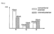
- FIG. 2 is a bar graph comparing current required to emit a given level of brightness by R, G and B pixels using different types of polarizers.
- FIG. 2 to emit 100 candela of brightness in an organic electroluminescent device 200 as shown in FIGs. 1A-B, using a colored polarizer 210 in accordance with an embodiment of the invention, only 40mA of current is supplied to the R pixel to achieve the desired 100 candela of brightness.
- power consumption requirements of the R pixel may be decreased by about 30mA.
- the current consumed by the G and B pixels may be slightly increased due to the red-color included in the colored polarizer 210, and so more current may need to be applied to emit acceptable levels of green light or blue light.
- the G and B pixels can emit the same level of brightness as the R pixel with only a small amount of additional current.
- the G pixel needs approximately 15mA of current, which is only about 5mA more than the current required by an electroluminescent device using a regular polarizer.
- the B pixel needs approximately 25mA of current, which is only about 5mA more than the current required by the device using a regular polarizer.
- the total current required by an organic electroluminescent device in accordance with an embodiment of the invention is approximately 80mA, which is approximately 20mA less than the current required by a device using a regular polarizer, whose total required current is approximately 100mA.
- the relationship between the levels of current which should be supplied to each of the R, G and B pixels in order to maintain a given level of brightness is substantially linear.
- a ratio may be applied to approximate the relative levels of current required to maintain a particular level of brightness.
- a ratio of the current required by the R pixel (70mA) to the current required by the G pixel (15mA) is approximately 2.6, compared to a ratio of 7 when using the regular polarizer.
- a ratio of the current required by the R pixel (70mA) to the current required by the B (25mA) pixel is approximately 1.6, compared to a ratio of 3.5 when using the regular polarizer.
- power consumption in accordance with an embodiment of the invention may be decreased for a given level of brightness by using a polarizer as described above and applying appropriate levels of current. Additionally, by controlling of a concentration of a red-colored substance in a colored polarizer of an organic electroluminescent device in accordance with an embodiment of the invention, power consumed by each of the R, G and B pixels may be controlled.
- the colored polarizer 210 may include substances having green-color, or blue-color. That is, the color of the polarizer 210 can be controlled based on desired brightness characteristics or main emitting color of an organic electroluminescent device in accordance with an embodiment of the invention.
- the electroluminescent device of the present invention may be used in or formed as flexible display for electronic books, newspapers, magazines, etc., different types of portable devices, e.g., handsets, MP3 players, notebook computers, etc., audio applications, navigation applications, televisions, monitors, or other types of devices using a display, either monochrome or color.
- portable devices e.g., handsets, MP3 players, notebook computers, etc.
- audio applications navigation applications
- the description of the present invention is intended to be illustrative, and not to limit the scope of the claims. Many alternatives, modifications, and variations will be apparent to those skilled in the art.
- means-plus-function clauses are intended to cover the structures described herein as performing the recited function and not only structural equivalents but also equivalent structures.
Landscapes
- Physics & Mathematics (AREA)
- Optics & Photonics (AREA)
- Electroluminescent Light Sources (AREA)
- Polarising Elements (AREA)
Abstract
Description
- The invention relates to a display device, and more particularly, an organic electroluminescent device.
- In an organic electroluminescent device, the brightness characteristics of the red pixels R are typically inferior to those of the green G and blue B pixels. Thus, more current should be applied the R pixels in order to emit the same level of brightness as the G and B pixels. For example, to emit 100 candela of brightness, 10mA current should be applied to the G pixel, and 20mA current should be applied to the B pixel. However, a 70mA current should be applied to the R pixel in order to emit 100 cadela of brightness. Thus, a great deal of current is required to emit the same level of brightness from the R, G and B pixels, thereby increasing the power consumption of the organic electroluminescent device. Therefore, there is a need to decrease power consumption requirements of organic electroluminescent devices while maintaining desired display characteristics
- An object of the invention is to solve at least the above problems and/or disadvantages and to provide at least the advantages described hereinafter.
- It is an object of the invention to minimize power consumption.
- Another object is to decrease total current required when the organic electroluminescent device emits.
- Another object of the invention is to provide an organic electroluminescent device which decreases current required at the time of emitting of the organic electroluminescent device by using a colored polarizer according to brightness characteristics of R, G and B pixels.
- To achieve these objects, in whole or in part, as embodied and broadly described herein, an organic electroluminescent device in accordance with an embodiment of the invention includes a substrate, an anode electrode layer, an organic layer, a cathode electrode layer and a colored polarizer, the colored polarizer polarizing light incident from the outside being adhered to a surface of the substrate contrary to an upper side of the substrate on which the anode electrode layer is formed.
- As described above, the organic electroluminescent device in accordance with embodiments of the present invention may minimize power consumption by decreasing total current required when the organic electroluminescent device emits. In addition, the organic electroluminescent device in accordance with embodiments of the invention uses a colored polarizer according to brightness characteristics of R, G and B pixels, thereby decreasing current required when the organic electroluminescent device emits.
- Additional advantages, objects, and features of the invention will be set forth in part in the description which follows and in part will become apparent to those having ordinary skill in the art upon examination of the following or may be learned from practice of the invention. The objects and advantages of the invention may be realized and attained as particularly pointed out in the appended claims.
- The invention will be described in detail with reference to the following drawings in which like reference numerals refer to like elements wherein:
- FIG. 1A is a sectional view of an organic electroluminescent device in accordance with an embodiment of the invention;
- FIG. 1B is an exemplary sectional view of an organic emitting layer of the organic electroluminescent device shown in FIG. 2A; and
- FIG. 2 is a bar graph comparing current required to emit a given level of brightness using different types of polarizers.
- The organic
electroluminescent device 200 shown in FIG. 1A includes asubstrate 202, ananode electrode layer 204, anorganic layer 206, acathode electrode layer 208 and acolored polarizer 210. Theanode electrode layer 204 may be provided on thesubstrate 202 by, for example, a deposition type process. - The
organic layer 206 may be provided on theanode electrode layer 204 by, for example, a deposition type process, and may include a hole injection layer (HIL), a hole transporting layer (HTL), an emitting layer (EML), an electron transporting layer (ETL), and an electron injection layer (EIL), as shown in FIG. 1 B. These layers of theorganic layer 206 may be formed in the sequence shown in FIG. 1B, however, other arrangements may also be appropriate. Thecathode electrode layer 208 may be formed from a metal such as, for example, aluminum (AI), and may be provided on theorganic layer 206 by, for example, a deposition type process. - Hereinafter, an emission process associated with the organic
electroluminescent device 200 will be described in detail. - The
anode electrode layer 204 provides holes to the HIL of theorganic emitting layer 206 if a certain positive voltage is applied thereto. Thecathode electrode layer 208 provides electrons to the EIL of theorganic emitting layer 206 if a certain negative voltage is applied thereto. The HIL smoothly injects the holes provided from theanode electrode layer 204 to the HTL, and the EIL smoothly injects the electrons provided from thecathode electrode layer 208 to the ETL. The HTL then transports the holes received from the HIL into the EML, and the ETL transports the electrons received from the EIL into the EML. The transported holes and electrons are recombined in the EML, and a light having a predetermined wavelength is from the EML of theorganic emitting layer 206 to the outside through thesubstrate 202 and thepolarizer 210. - The
polarizer 210 may be provided on a surface of thesubstrate 202 which is opposite an upper surface of thesubstrate 202 on which theanode electrode layer 204 is provided, that is, a lower surface of thesubstrate 202, as shown in FIG. 1A. However, other positions for thepolarizer 210 may also be appropriate. For example, thepolarizer 210 may be provided between thesubstrate 202 and theanode electrode layer 204. Thepolarizer 210 transmits the light emitted by EML with a given transmissivity, and may also intercept light reflected from thecathode electrode layer 208, thereby improving contrast in the image displayed by the organicelectroluminescent device 200. - The
polarizer 210 in accordance with an embodiment of the invention may include a red-colored substance. If the brightness characteristics of the R pixel are inferior to those of the G and B pixels, then more current would have to be applied to the R to yield the same brightness. However, by using acolored polarizer 210 which includes a red-colored substance, emission of red color from the R pixels may be improved when compared to a regular polarizer without applying additional current to the R pixels. - Thus, an organic
electroluminescent device 200 which includes this type ofcolored polarizer 210, in accordance with an embodiment of the invention, can emit red light at the same level of brightness as the green and blue light without increased power consumption. Thus, power consumption requirements of the R pixel for a given level of brightness may be decreased. - FIG. 2 is a bar graph comparing current required to emit a given level of brightness by R, G and B pixels using different types of polarizers. As shown in FIG. 2, to emit 100 candela of brightness in an organic
electroluminescent device 200 as shown in FIGs. 1A-B, using acolored polarizer 210 in accordance with an embodiment of the invention, only 40mA of current is supplied to the R pixel to achieve the desired 100 candela of brightness. Thus, compared to the regular polarizer, power consumption requirements of the R pixel may be decreased by about 30mA. - This may cause the current consumed by the G and B pixels to be slightly increased due to the red-color included in the
colored polarizer 210, and so more current may need to be applied to emit acceptable levels of green light or blue light. However, as the G and B pixels have higher brightness characteristics, the G and B pixels can emit the same level of brightness as the R pixel with only a small amount of additional current. - For example, in order to emit 100 candela of brightness from the organic
electroluminescent device 200 in accordance with an embodiment of the invention, the G pixel needs approximately 15mA of current, which is only about 5mA more than the current required by an electroluminescent device using a regular polarizer. Likewise, to emit 100 candela of brightness, the B pixel needs approximately 25mA of current, which is only about 5mA more than the current required by the device using a regular polarizer. Accordingly, to emit 100 candela of brightness, the total current required by an organic electroluminescent device in accordance with an embodiment of the invention is approximately 80mA, which is approximately 20mA less than the current required by a device using a regular polarizer, whose total required current is approximately 100mA. - The relationship between the levels of current which should be supplied to each of the R, G and B pixels in order to maintain a given level of brightness, such as, for example, the 100 candela of brightness shown in FIG. 2, is substantially linear. Thus, a ratio may be applied to approximate the relative levels of current required to maintain a particular level of brightness. For example, based on the exemplary data shown in FIG. 2, a ratio of the current required by the R pixel (70mA) to the current required by the G pixel (15mA) is approximately 2.6, compared to a ratio of 7 when using the regular polarizer. Likewise, a ratio of the current required by the R pixel (70mA) to the current required by the B (25mA) pixel is approximately 1.6, compared to a ratio of 3.5 when using the regular polarizer.
- Thus, power consumption in accordance with an embodiment of the invention may be decreased for a given level of brightness by using a polarizer as described above and applying appropriate levels of current. Additionally, by controlling of a concentration of a red-colored substance in a colored polarizer of an organic electroluminescent device in accordance with an embodiment of the invention, power consumed by each of the R, G and B pixels may be controlled.
- Additionally, the
colored polarizer 210 may include substances having green-color, or blue-color. That is, the color of thepolarizer 210 can be controlled based on desired brightness characteristics or main emitting color of an organic electroluminescent device in accordance with an embodiment of the invention. - The foregoing embodiments and advantages are merely exemplary and are not to be construed as limiting the present invention. The present teaching can be readily applied to other types of apparatuses. The electroluminescent device of the present invention may be used in or formed as flexible display for electronic books, newspapers, magazines, etc., different types of portable devices, e.g., handsets, MP3 players, notebook computers, etc., audio applications, navigation applications, televisions, monitors, or other types of devices using a display, either monochrome or color. The description of the present invention is intended to be illustrative, and not to limit the scope of the claims. Many alternatives, modifications, and variations will be apparent to those skilled in the art. In the claims, means-plus-function clauses are intended to cover the structures described herein as performing the recited function and not only structural equivalents but also equivalent structures.
Claims (21)
- An electroluminescent device, comprising:a substrate having first and second surfaces, the first and second surfaces being different surfaces;an anode layer over the first surface;an electroluminescent layer provided on the anode layer;a cathode layer provided on the electroluminescent layer; anda polarizer provided on at least one of the first surface or the second surface of the substrate, wherein the polarizer includes a colored substance corresponding to a color of light emitted by the electroluminescent layer.
- The device of claim 1, wherein the colored substance is one of red, green, or blue.
- The device of claim 1, wherein the colored substance is red so as to increase a transmittance level of red light for a predetermined level of current.
- The device of claim 1, wherein the color of the colored substance corresponds to a color of a sub-pixel of a plurality of pixels of the electroluminescent device which requires the highest level of current to emit a predetermined level of brightness.
- The device of claim 1, wherein the polarizer is coupled to a surface of the substrate which is opposite a surface to which the anode electrode layer is coupled.
- The device of claim 1, wherein the polarizer positioned between a surface of the substrate and the anode electrode layer.
- The device of claim 1, wherein the polarizer is a circular polarizer.
- The device of claim 7, wherein the polarizer is configured to polarize light incident on the device from the outside so as to maintain light emitted by the device at a predetermined level of brightness.
- The device of claim 8, wherein the cathode electrode layer is configured to reflect light incident thereon, and the polarizer is configured to emit light reflected by the cathode electrode layer so as to maintain the predetermined level of brightness.
- The device of claim 1, wherein the electroluminescent layer is an organic electroluminescent layer.
- A method of operating an electroluminescent device, comprising:providing a first current to produce a corresponding first color of light;providing a second current to produce a corresponding second color of light; andproviding a third current to produce a corresponding third color of light, wherein a magnitude of the first current is less than approximately 7 times a magnitude of the second current, and less than approximately 3.5 times a magnitude of the third current.
- The method of claim 11, wherein the magnitude of the first current is between approximately 2 and 7 times the magnitude of the second current.
- The method of claim 12, wherein the magnitude of the first current is approximately 2.6 times the magnitude of the second current.
- The method of claim 11, wherein the magnitude of the first current is between approximately 1.5 and 3.5 times the magnitude of the third current.
- The method of claim 14, wherein the magnitude of the first current is approximately 1.6 times the magnitude of the third current.
- The method of claim 11, wherein providing a first current to produce a corresponding first color of light comprises applying the first current to a red emission area of the device so as to produce red light.
- The method of claim 16, wherein providing a second current to produce a corresponding second color of light comprises applying the second current to a green emission area of the device so as to produce green light.
- The method of claim 17, wherein providing a third current to produce a corresponding third color of light comprises applying the first current to a blue emission area of the device so as to produce blue light.
- The method of claim 11, further comprising emitting the first, second and third colors of light through a polarizer including a colored substance corresponding to one of the first, second or third colors of light.
- The method of claim 19, wherein the polarizer includes a red colored substance configured to increase a transmission of red light.
- The method of claim 19, further comprising selecting the colored substance based on a pixel color of the device which requires the highest current to produce a given level of brightness.
Applications Claiming Priority (1)
| Application Number | Priority Date | Filing Date | Title |
|---|---|---|---|
| KR1020050076384A KR100729855B1 (en) | 2005-08-19 | 2005-08-19 | Organic electroluminescent element |
Publications (3)
| Publication Number | Publication Date |
|---|---|
| EP1755179A2 true EP1755179A2 (en) | 2007-02-21 |
| EP1755179A3 EP1755179A3 (en) | 2010-11-24 |
| EP1755179B1 EP1755179B1 (en) | 2014-05-07 |
Family
ID=37440835
Family Applications (1)
| Application Number | Title | Priority Date | Filing Date |
|---|---|---|---|
| EP05027949.6A Expired - Lifetime EP1755179B1 (en) | 2005-08-19 | 2005-12-20 | Method of operating an electroluminescent device |
Country Status (5)
| Country | Link |
|---|---|
| US (2) | US7671531B2 (en) |
| EP (1) | EP1755179B1 (en) |
| JP (1) | JP5112631B2 (en) |
| KR (1) | KR100729855B1 (en) |
| CN (1) | CN100559628C (en) |
Families Citing this family (3)
| Publication number | Priority date | Publication date | Assignee | Title |
|---|---|---|---|---|
| JP4912437B2 (en) * | 2008-08-05 | 2012-04-11 | 三星モバイルディスプレイ株式會社 | Organic light emitting display |
| CN105810843B (en) * | 2016-03-15 | 2018-03-13 | 深圳市华星光电技术有限公司 | Luminescent device, backlight module and display device |
| CN107394050B (en) * | 2017-07-19 | 2019-08-02 | 京东方科技集团股份有限公司 | A kind of OLED display panel, display device and control method thereof |
Family Cites Families (23)
| Publication number | Priority date | Publication date | Assignee | Title |
|---|---|---|---|---|
| DE3244885A1 (en) * | 1982-12-02 | 1984-06-07 | Merck Patent Gmbh, 6100 Darmstadt | COLOR SELECTIVE CIRCULAR POLARIZER AND ITS USE |
| JPH0666018B2 (en) * | 1987-01-09 | 1994-08-24 | 株式会社日立製作所 | LCD projection device |
| JP4477150B2 (en) * | 1996-01-17 | 2010-06-09 | 三星モバイルディスプレイ株式會社 | Organic thin film EL device |
| KR100624045B1 (en) * | 1998-12-01 | 2006-09-18 | 코닌클리케 필립스 일렉트로닉스 엔.브이. | Color filter layers of cholesterically arranged materials, and reflective LCs provided with such color filter layers |
| JP2001035653A (en) * | 1999-07-21 | 2001-02-09 | Nec Corp | Organic EL panel and its filter |
| US6936485B2 (en) * | 2000-03-27 | 2005-08-30 | Semiconductor Energy Laboratory Co., Ltd. | Method of manufacturing a light emitting device |
| US6838819B2 (en) * | 2000-06-19 | 2005-01-04 | Lg Electronics Inc. | Full color organic EL display panel, manufacturing method thereof and driving circuit thereof |
| US6825820B2 (en) * | 2000-08-10 | 2004-11-30 | Semiconductor Energy Laboratory Co., Ltd. | Display device and electronic device |
| KR100697373B1 (en) * | 2000-12-20 | 2007-03-20 | 비오이 하이디스 테크놀로지 주식회사 | Double-sided light emitting display device and manufacturing method |
| JP4011292B2 (en) * | 2001-01-15 | 2007-11-21 | 株式会社日立製作所 | LIGHT EMITTING ELEMENT AND DISPLAY DEVICE |
| JP3508753B2 (en) * | 2001-10-15 | 2004-03-22 | ソニー株式会社 | Image display device |
| JP2003282235A (en) * | 2002-03-25 | 2003-10-03 | Sanyo Electric Co Ltd | Organic electroluminescence display device |
| CN1656627A (en) * | 2002-05-31 | 2005-08-17 | 皇家飞利浦电子股份有限公司 | Electroluminescent device |
| WO2004036299A1 (en) * | 2002-10-14 | 2004-04-29 | Koninklijke Philips Electronics N.V. | Color filter and liquid crystal display device comprising such filter |
| JP2004207136A (en) * | 2002-12-26 | 2004-07-22 | Nitto Denko Corp | Surface light source and display device using the same |
| US7030555B2 (en) * | 2003-04-04 | 2006-04-18 | Nitto Denko Corporation | Organic electroluminescence device, planar light source and display device using the same |
| US7385223B2 (en) * | 2003-04-24 | 2008-06-10 | Samsung Sdi Co., Ltd. | Flat panel display with thin film transistor |
| TWI245130B (en) * | 2003-05-02 | 2005-12-11 | Optimax Tech Corp | Color compensational layer's structure and manufacturing method thereof |
| JP4098747B2 (en) * | 2003-05-28 | 2008-06-11 | 三星エスディアイ株式会社 | Double-sided light emitting display |
| US7632291B2 (en) * | 2003-06-13 | 2009-12-15 | Trivascular2, Inc. | Inflatable implant |
| GB2410600A (en) * | 2004-01-30 | 2005-08-03 | Cambridge Display Tech Ltd | Organic light emitting diode display device |
| CN2682768Y (en) * | 2004-02-26 | 2005-03-02 | 力特光电科技股份有限公司 | Panel Structure of Color Organic Light Emitting Diodes |
| JP4695345B2 (en) * | 2004-05-18 | 2011-06-08 | 株式会社 日立ディスプレイズ | Organic electroluminescence display device |
-
2005
- 2005-08-19 KR KR1020050076384A patent/KR100729855B1/en not_active Expired - Lifetime
- 2005-12-20 EP EP05027949.6A patent/EP1755179B1/en not_active Expired - Lifetime
- 2005-12-22 JP JP2005369990A patent/JP5112631B2/en not_active Expired - Lifetime
- 2005-12-23 CN CNB2005101358202A patent/CN100559628C/en not_active Expired - Lifetime
- 2005-12-27 US US11/316,730 patent/US7671531B2/en active Active
-
2009
- 2009-12-31 US US12/650,942 patent/US8207666B2/en not_active Expired - Lifetime
Also Published As
| Publication number | Publication date |
|---|---|
| US7671531B2 (en) | 2010-03-02 |
| JP5112631B2 (en) | 2013-01-09 |
| JP2007053069A (en) | 2007-03-01 |
| EP1755179B1 (en) | 2014-05-07 |
| KR20070021765A (en) | 2007-02-23 |
| US20100141171A1 (en) | 2010-06-10 |
| US8207666B2 (en) | 2012-06-26 |
| US20070040495A1 (en) | 2007-02-22 |
| KR100729855B1 (en) | 2007-06-18 |
| CN1917252A (en) | 2007-02-21 |
| EP1755179A3 (en) | 2010-11-24 |
| CN100559628C (en) | 2009-11-11 |
Similar Documents
| Publication | Publication Date | Title |
|---|---|---|
| US10797115B2 (en) | Display panel and display apparatus using the same | |
| US10504970B2 (en) | Organic light emitting diode display with color filters having recess portion or convex portion | |
| US9443913B2 (en) | Method of tuning display chromaticity by mixing color filter materials and device having mixed color filter materials | |
| CN107591425A (en) | AMOLED display panels and display device | |
| WO2016117181A1 (en) | Display device and electronic apparatus | |
| KR20140082551A (en) | Organic light emitting display and method for fabricating the same | |
| CN104617226A (en) | Array substrate and manufacturing method thereof as well as display device and display compensation method | |
| US20220069024A1 (en) | Display panel and manufacturing method thereof and display apparatus | |
| US20060006797A1 (en) | Lighting apparatus and liquid crystal display apparatus | |
| CN108063156A (en) | Pixel unit and its control method, display device | |
| US8207666B2 (en) | Organic electroluminescent device with enhanced light emission | |
| US7659664B2 (en) | System for displaying image | |
| JP4411288B2 (en) | Display device | |
| KR20000073118A (en) | Organic electroluminescent display device | |
| US10249686B2 (en) | Organic light-emitting device and method of manufacturing the same | |
| US20070159087A1 (en) | Organic light-emitting device | |
| KR100565742B1 (en) | Organic light emitting diode | |
| KR100722115B1 (en) | Organic electroluminescent display | |
| JP2005317296A (en) | Lighting equipment | |
| US8143779B2 (en) | System for displaying images employing tandem electroluminescent device | |
| US20060033424A1 (en) | Dual emissive electroluminescent displays and fabricating and display methods thereof | |
| KR100734058B1 (en) | Organic EL device and method of manufacturing polarizing plate used therein | |
| JP2007141790A (en) | Display device | |
| JP2003223141A (en) | Luminance control method of organic EL display and organic EL display | |
| KR20170043136A (en) | Organic light emitting diode display |
Legal Events
| Date | Code | Title | Description |
|---|---|---|---|
| PUAI | Public reference made under article 153(3) epc to a published international application that has entered the european phase |
Free format text: ORIGINAL CODE: 0009012 |
|
| 17P | Request for examination filed |
Effective date: 20051220 |
|
| AK | Designated contracting states |
Kind code of ref document: A2 Designated state(s): AT BE BG CH CY CZ DE DK EE ES FI FR GB GR HU IE IS IT LI LT LU LV MC NL PL PT RO SE SI SK TR |
|
| AX | Request for extension of the european patent |
Extension state: AL BA HR MK YU |
|
| RAP1 | Party data changed (applicant data changed or rights of an application transferred) |
Owner name: LG DISPLAY CO., LTD. |
|
| RAP1 | Party data changed (applicant data changed or rights of an application transferred) |
Owner name: LG DISPLAY CO., LTD. |
|
| PUAL | Search report despatched |
Free format text: ORIGINAL CODE: 0009013 |
|
| AK | Designated contracting states |
Kind code of ref document: A3 Designated state(s): AT BE BG CH CY CZ DE DK EE ES FI FR GB GR HU IE IS IT LI LT LU LV MC NL PL PT RO SE SI SK TR |
|
| AX | Request for extension of the european patent |
Extension state: AL BA HR MK YU |
|
| AKX | Designation fees paid |
Designated state(s): AT BE BG CH CY CZ DE DK EE ES FI FR GB GR HU IE IS IT LI LT LU LV MC NL PL PT RO SE SI SK TR |
|
| 17Q | First examination report despatched |
Effective date: 20130102 |
|
| RIC1 | Information provided on ipc code assigned before grant |
Ipc: H01L 27/32 20060101ALI20131011BHEP Ipc: H01L 51/52 20060101AFI20131011BHEP |
|
| GRAP | Despatch of communication of intention to grant a patent |
Free format text: ORIGINAL CODE: EPIDOSNIGR1 |
|
| INTG | Intention to grant announced |
Effective date: 20131128 |
|
| GRAS | Grant fee paid |
Free format text: ORIGINAL CODE: EPIDOSNIGR3 |
|
| GRAA | (expected) grant |
Free format text: ORIGINAL CODE: 0009210 |
|
| AK | Designated contracting states |
Kind code of ref document: B1 Designated state(s): AT BE BG CH CY CZ DE DK EE ES FI FR GB GR HU IE IS IT LI LT LU LV MC NL PL PT RO SE SI SK TR |
|
| REG | Reference to a national code |
Ref country code: GB Ref legal event code: FG4D |
|
| REG | Reference to a national code |
Ref country code: AT Ref legal event code: REF Ref document number: 667270 Country of ref document: AT Kind code of ref document: T Effective date: 20140515 |
|
| REG | Reference to a national code |
Ref country code: IE Ref legal event code: FG4D |
|
| REG | Reference to a national code |
Ref country code: DE Ref legal event code: R096 Ref document number: 602005043512 Country of ref document: DE Effective date: 20140612 |
|
| REG | Reference to a national code |
Ref country code: NL Ref legal event code: T3 |
|
| REG | Reference to a national code |
Ref country code: AT Ref legal event code: MK05 Ref document number: 667270 Country of ref document: AT Kind code of ref document: T Effective date: 20140507 |
|
| REG | Reference to a national code |
Ref country code: LT Ref legal event code: MG4D |
|
| PG25 | Lapsed in a contracting state [announced via postgrant information from national office to epo] |
Ref country code: LT Free format text: LAPSE BECAUSE OF FAILURE TO SUBMIT A TRANSLATION OF THE DESCRIPTION OR TO PAY THE FEE WITHIN THE PRESCRIBED TIME-LIMIT Effective date: 20140507 Ref country code: CY Free format text: LAPSE BECAUSE OF FAILURE TO SUBMIT A TRANSLATION OF THE DESCRIPTION OR TO PAY THE FEE WITHIN THE PRESCRIBED TIME-LIMIT Effective date: 20140507 Ref country code: IS Free format text: LAPSE BECAUSE OF FAILURE TO SUBMIT A TRANSLATION OF THE DESCRIPTION OR TO PAY THE FEE WITHIN THE PRESCRIBED TIME-LIMIT Effective date: 20140907 Ref country code: GR Free format text: LAPSE BECAUSE OF FAILURE TO SUBMIT A TRANSLATION OF THE DESCRIPTION OR TO PAY THE FEE WITHIN THE PRESCRIBED TIME-LIMIT Effective date: 20140808 Ref country code: FI Free format text: LAPSE BECAUSE OF FAILURE TO SUBMIT A TRANSLATION OF THE DESCRIPTION OR TO PAY THE FEE WITHIN THE PRESCRIBED TIME-LIMIT Effective date: 20140507 |
|
| PG25 | Lapsed in a contracting state [announced via postgrant information from national office to epo] |
Ref country code: LV Free format text: LAPSE BECAUSE OF FAILURE TO SUBMIT A TRANSLATION OF THE DESCRIPTION OR TO PAY THE FEE WITHIN THE PRESCRIBED TIME-LIMIT Effective date: 20140507 Ref country code: AT Free format text: LAPSE BECAUSE OF FAILURE TO SUBMIT A TRANSLATION OF THE DESCRIPTION OR TO PAY THE FEE WITHIN THE PRESCRIBED TIME-LIMIT Effective date: 20140507 Ref country code: ES Free format text: LAPSE BECAUSE OF FAILURE TO SUBMIT A TRANSLATION OF THE DESCRIPTION OR TO PAY THE FEE WITHIN THE PRESCRIBED TIME-LIMIT Effective date: 20140507 Ref country code: PL Free format text: LAPSE BECAUSE OF FAILURE TO SUBMIT A TRANSLATION OF THE DESCRIPTION OR TO PAY THE FEE WITHIN THE PRESCRIBED TIME-LIMIT Effective date: 20140507 Ref country code: SE Free format text: LAPSE BECAUSE OF FAILURE TO SUBMIT A TRANSLATION OF THE DESCRIPTION OR TO PAY THE FEE WITHIN THE PRESCRIBED TIME-LIMIT Effective date: 20140507 |
|
| PG25 | Lapsed in a contracting state [announced via postgrant information from national office to epo] |
Ref country code: PT Free format text: LAPSE BECAUSE OF FAILURE TO SUBMIT A TRANSLATION OF THE DESCRIPTION OR TO PAY THE FEE WITHIN THE PRESCRIBED TIME-LIMIT Effective date: 20140908 |
|
| PG25 | Lapsed in a contracting state [announced via postgrant information from national office to epo] |
Ref country code: EE Free format text: LAPSE BECAUSE OF FAILURE TO SUBMIT A TRANSLATION OF THE DESCRIPTION OR TO PAY THE FEE WITHIN THE PRESCRIBED TIME-LIMIT Effective date: 20140507 Ref country code: SK Free format text: LAPSE BECAUSE OF FAILURE TO SUBMIT A TRANSLATION OF THE DESCRIPTION OR TO PAY THE FEE WITHIN THE PRESCRIBED TIME-LIMIT Effective date: 20140507 Ref country code: CZ Free format text: LAPSE BECAUSE OF FAILURE TO SUBMIT A TRANSLATION OF THE DESCRIPTION OR TO PAY THE FEE WITHIN THE PRESCRIBED TIME-LIMIT Effective date: 20140507 Ref country code: DK Free format text: LAPSE BECAUSE OF FAILURE TO SUBMIT A TRANSLATION OF THE DESCRIPTION OR TO PAY THE FEE WITHIN THE PRESCRIBED TIME-LIMIT Effective date: 20140507 Ref country code: BE Free format text: LAPSE BECAUSE OF FAILURE TO SUBMIT A TRANSLATION OF THE DESCRIPTION OR TO PAY THE FEE WITHIN THE PRESCRIBED TIME-LIMIT Effective date: 20140507 Ref country code: RO Free format text: LAPSE BECAUSE OF FAILURE TO SUBMIT A TRANSLATION OF THE DESCRIPTION OR TO PAY THE FEE WITHIN THE PRESCRIBED TIME-LIMIT Effective date: 20140507 |
|
| REG | Reference to a national code |
Ref country code: DE Ref legal event code: R097 Ref document number: 602005043512 Country of ref document: DE |
|
| PLBE | No opposition filed within time limit |
Free format text: ORIGINAL CODE: 0009261 |
|
| STAA | Information on the status of an ep patent application or granted ep patent |
Free format text: STATUS: NO OPPOSITION FILED WITHIN TIME LIMIT |
|
| 26N | No opposition filed |
Effective date: 20150210 |
|
| PG25 | Lapsed in a contracting state [announced via postgrant information from national office to epo] |
Ref country code: IT Free format text: LAPSE BECAUSE OF FAILURE TO SUBMIT A TRANSLATION OF THE DESCRIPTION OR TO PAY THE FEE WITHIN THE PRESCRIBED TIME-LIMIT Effective date: 20140507 |
|
| REG | Reference to a national code |
Ref country code: DE Ref legal event code: R097 Ref document number: 602005043512 Country of ref document: DE Effective date: 20150210 |
|
| PG25 | Lapsed in a contracting state [announced via postgrant information from national office to epo] |
Ref country code: SI Free format text: LAPSE BECAUSE OF FAILURE TO SUBMIT A TRANSLATION OF THE DESCRIPTION OR TO PAY THE FEE WITHIN THE PRESCRIBED TIME-LIMIT Effective date: 20140507 Ref country code: LU Free format text: LAPSE BECAUSE OF FAILURE TO SUBMIT A TRANSLATION OF THE DESCRIPTION OR TO PAY THE FEE WITHIN THE PRESCRIBED TIME-LIMIT Effective date: 20141220 |
|
| REG | Reference to a national code |
Ref country code: CH Ref legal event code: PL |
|
| REG | Reference to a national code |
Ref country code: IE Ref legal event code: MM4A |
|
| REG | Reference to a national code |
Ref country code: FR Ref legal event code: PLFP Year of fee payment: 11 |
|
| PG25 | Lapsed in a contracting state [announced via postgrant information from national office to epo] |
Ref country code: CH Free format text: LAPSE BECAUSE OF NON-PAYMENT OF DUE FEES Effective date: 20141231 Ref country code: LI Free format text: LAPSE BECAUSE OF NON-PAYMENT OF DUE FEES Effective date: 20141231 Ref country code: IE Free format text: LAPSE BECAUSE OF NON-PAYMENT OF DUE FEES Effective date: 20141220 |
|
| PG25 | Lapsed in a contracting state [announced via postgrant information from national office to epo] |
Ref country code: MC Free format text: LAPSE BECAUSE OF FAILURE TO SUBMIT A TRANSLATION OF THE DESCRIPTION OR TO PAY THE FEE WITHIN THE PRESCRIBED TIME-LIMIT Effective date: 20140507 Ref country code: BG Free format text: LAPSE BECAUSE OF FAILURE TO SUBMIT A TRANSLATION OF THE DESCRIPTION OR TO PAY THE FEE WITHIN THE PRESCRIBED TIME-LIMIT Effective date: 20140507 |
|
| PG25 | Lapsed in a contracting state [announced via postgrant information from national office to epo] |
Ref country code: TR Free format text: LAPSE BECAUSE OF FAILURE TO SUBMIT A TRANSLATION OF THE DESCRIPTION OR TO PAY THE FEE WITHIN THE PRESCRIBED TIME-LIMIT Effective date: 20140507 Ref country code: HU Free format text: LAPSE BECAUSE OF FAILURE TO SUBMIT A TRANSLATION OF THE DESCRIPTION OR TO PAY THE FEE WITHIN THE PRESCRIBED TIME-LIMIT; INVALID AB INITIO Effective date: 20051220 |
|
| REG | Reference to a national code |
Ref country code: FR Ref legal event code: PLFP Year of fee payment: 12 |
|
| REG | Reference to a national code |
Ref country code: FR Ref legal event code: PLFP Year of fee payment: 13 |
|
| REG | Reference to a national code |
Ref country code: FR Ref legal event code: PLFP Year of fee payment: 14 |
|
| REG | Reference to a national code |
Ref country code: DE Ref legal event code: R079 Ref document number: 602005043512 Country of ref document: DE Free format text: PREVIOUS MAIN CLASS: H01L0051520000 Ipc: H10K0050800000 |
|
| PGFP | Annual fee paid to national office [announced via postgrant information from national office to epo] |
Ref country code: NL Payment date: 20241021 Year of fee payment: 20 |
|
| PGFP | Annual fee paid to national office [announced via postgrant information from national office to epo] |
Ref country code: DE Payment date: 20241021 Year of fee payment: 20 |
|
| PGFP | Annual fee paid to national office [announced via postgrant information from national office to epo] |
Ref country code: GB Payment date: 20241022 Year of fee payment: 20 |
|
| PGFP | Annual fee paid to national office [announced via postgrant information from national office to epo] |
Ref country code: FR Payment date: 20241022 Year of fee payment: 20 |
|
| REG | Reference to a national code |
Ref country code: DE Ref legal event code: R071 Ref document number: 602005043512 Country of ref document: DE |
|
| REG | Reference to a national code |
Ref country code: NL Ref legal event code: MK Effective date: 20251219 |
|
| REG | Reference to a national code |
Ref country code: GB Ref legal event code: PE20 Expiry date: 20251219 |