EP1755154B1 - Method for manufacturing a zinc oxide thin film at low temperatures - Google Patents
Method for manufacturing a zinc oxide thin film at low temperatures Download PDFInfo
- Publication number
- EP1755154B1 EP1755154B1 EP06005550A EP06005550A EP1755154B1 EP 1755154 B1 EP1755154 B1 EP 1755154B1 EP 06005550 A EP06005550 A EP 06005550A EP 06005550 A EP06005550 A EP 06005550A EP 1755154 B1 EP1755154 B1 EP 1755154B1
- Authority
- EP
- European Patent Office
- Prior art keywords
- substrate
- zinc oxide
- thin film
- oxide thin
- zinc
- Prior art date
- Legal status (The legal status is an assumption and is not a legal conclusion. Google has not performed a legal analysis and makes no representation as to the accuracy of the status listed.)
- Expired - Lifetime
Links
Images








Classifications
-
- C—CHEMISTRY; METALLURGY
- C23—COATING METALLIC MATERIAL; COATING MATERIAL WITH METALLIC MATERIAL; CHEMICAL SURFACE TREATMENT; DIFFUSION TREATMENT OF METALLIC MATERIAL; COATING BY VACUUM EVAPORATION, BY SPUTTERING, BY ION IMPLANTATION OR BY CHEMICAL VAPOUR DEPOSITION, IN GENERAL; INHIBITING CORROSION OF METALLIC MATERIAL OR INCRUSTATION IN GENERAL
- C23C—COATING METALLIC MATERIAL; COATING MATERIAL WITH METALLIC MATERIAL; SURFACE TREATMENT OF METALLIC MATERIAL BY DIFFUSION INTO THE SURFACE, BY CHEMICAL CONVERSION OR SUBSTITUTION; COATING BY VACUUM EVAPORATION, BY SPUTTERING, BY ION IMPLANTATION OR BY CHEMICAL VAPOUR DEPOSITION, IN GENERAL
- C23C14/00—Coating by vacuum evaporation, by sputtering or by ion implantation of the coating forming material
- C23C14/0021—Reactive sputtering or evaporation
- C23C14/0026—Activation or excitation of reactive gases outside the coating chamber
-
- C—CHEMISTRY; METALLURGY
- C23—COATING METALLIC MATERIAL; COATING MATERIAL WITH METALLIC MATERIAL; CHEMICAL SURFACE TREATMENT; DIFFUSION TREATMENT OF METALLIC MATERIAL; COATING BY VACUUM EVAPORATION, BY SPUTTERING, BY ION IMPLANTATION OR BY CHEMICAL VAPOUR DEPOSITION, IN GENERAL; INHIBITING CORROSION OF METALLIC MATERIAL OR INCRUSTATION IN GENERAL
- C23C—COATING METALLIC MATERIAL; COATING MATERIAL WITH METALLIC MATERIAL; SURFACE TREATMENT OF METALLIC MATERIAL BY DIFFUSION INTO THE SURFACE, BY CHEMICAL CONVERSION OR SUBSTITUTION; COATING BY VACUUM EVAPORATION, BY SPUTTERING, BY ION IMPLANTATION OR BY CHEMICAL VAPOUR DEPOSITION, IN GENERAL
- C23C16/00—Chemical coating by decomposition of gaseous compounds, without leaving reaction products of surface material in the coating, i.e. chemical vapour deposition [CVD] processes
- C23C16/22—Chemical coating by decomposition of gaseous compounds, without leaving reaction products of surface material in the coating, i.e. chemical vapour deposition [CVD] processes characterised by the deposition of inorganic material, other than metallic material
- C23C16/30—Deposition of compounds, mixtures or solid solutions, e.g. borides, carbides, nitrides
- C23C16/40—Oxides
-
- C—CHEMISTRY; METALLURGY
- C23—COATING METALLIC MATERIAL; COATING MATERIAL WITH METALLIC MATERIAL; CHEMICAL SURFACE TREATMENT; DIFFUSION TREATMENT OF METALLIC MATERIAL; COATING BY VACUUM EVAPORATION, BY SPUTTERING, BY ION IMPLANTATION OR BY CHEMICAL VAPOUR DEPOSITION, IN GENERAL; INHIBITING CORROSION OF METALLIC MATERIAL OR INCRUSTATION IN GENERAL
- C23C—COATING METALLIC MATERIAL; COATING MATERIAL WITH METALLIC MATERIAL; SURFACE TREATMENT OF METALLIC MATERIAL BY DIFFUSION INTO THE SURFACE, BY CHEMICAL CONVERSION OR SUBSTITUTION; COATING BY VACUUM EVAPORATION, BY SPUTTERING, BY ION IMPLANTATION OR BY CHEMICAL VAPOUR DEPOSITION, IN GENERAL
- C23C14/00—Coating by vacuum evaporation, by sputtering or by ion implantation of the coating forming material
- C23C14/06—Coating by vacuum evaporation, by sputtering or by ion implantation of the coating forming material characterised by the coating material
- C23C14/08—Oxides
- C23C14/086—Oxides of zinc, germanium, cadmium, indium, tin, thallium or bismuth
-
- C—CHEMISTRY; METALLURGY
- C23—COATING METALLIC MATERIAL; COATING MATERIAL WITH METALLIC MATERIAL; CHEMICAL SURFACE TREATMENT; DIFFUSION TREATMENT OF METALLIC MATERIAL; COATING BY VACUUM EVAPORATION, BY SPUTTERING, BY ION IMPLANTATION OR BY CHEMICAL VAPOUR DEPOSITION, IN GENERAL; INHIBITING CORROSION OF METALLIC MATERIAL OR INCRUSTATION IN GENERAL
- C23C—COATING METALLIC MATERIAL; COATING MATERIAL WITH METALLIC MATERIAL; SURFACE TREATMENT OF METALLIC MATERIAL BY DIFFUSION INTO THE SURFACE, BY CHEMICAL CONVERSION OR SUBSTITUTION; COATING BY VACUUM EVAPORATION, BY SPUTTERING, BY ION IMPLANTATION OR BY CHEMICAL VAPOUR DEPOSITION, IN GENERAL
- C23C16/00—Chemical coating by decomposition of gaseous compounds, without leaving reaction products of surface material in the coating, i.e. chemical vapour deposition [CVD] processes
-
- H—ELECTRICITY
- H10—SEMICONDUCTOR DEVICES; ELECTRIC SOLID-STATE DEVICES NOT OTHERWISE PROVIDED FOR
- H10P—GENERIC PROCESSES OR APPARATUS FOR THE MANUFACTURE OR TREATMENT OF DEVICES COVERED BY CLASS H10
- H10P14/00—Formation of materials, e.g. in the shape of layers or pillars
- H10P14/20—Formation of materials, e.g. in the shape of layers or pillars of semiconductor materials
- H10P14/22—Formation of materials, e.g. in the shape of layers or pillars of semiconductor materials using physical deposition, e.g. vacuum deposition or sputtering
-
- H—ELECTRICITY
- H10—SEMICONDUCTOR DEVICES; ELECTRIC SOLID-STATE DEVICES NOT OTHERWISE PROVIDED FOR
- H10P—GENERIC PROCESSES OR APPARATUS FOR THE MANUFACTURE OR TREATMENT OF DEVICES COVERED BY CLASS H10
- H10P14/00—Formation of materials, e.g. in the shape of layers or pillars
- H10P14/20—Formation of materials, e.g. in the shape of layers or pillars of semiconductor materials
- H10P14/29—Formation of materials, e.g. in the shape of layers or pillars of semiconductor materials characterised by the substrates
- H10P14/2901—Materials
- H10P14/2907—Materials being Group IIIA-VA materials
- H10P14/2911—Arsenides
-
- H—ELECTRICITY
- H10—SEMICONDUCTOR DEVICES; ELECTRIC SOLID-STATE DEVICES NOT OTHERWISE PROVIDED FOR
- H10P—GENERIC PROCESSES OR APPARATUS FOR THE MANUFACTURE OR TREATMENT OF DEVICES COVERED BY CLASS H10
- H10P14/00—Formation of materials, e.g. in the shape of layers or pillars
- H10P14/20—Formation of materials, e.g. in the shape of layers or pillars of semiconductor materials
- H10P14/29—Formation of materials, e.g. in the shape of layers or pillars of semiconductor materials characterised by the substrates
- H10P14/2901—Materials
- H10P14/2922—Materials being non-crystalline insulating materials, e.g. glass or polymers
-
- H—ELECTRICITY
- H10—SEMICONDUCTOR DEVICES; ELECTRIC SOLID-STATE DEVICES NOT OTHERWISE PROVIDED FOR
- H10P—GENERIC PROCESSES OR APPARATUS FOR THE MANUFACTURE OR TREATMENT OF DEVICES COVERED BY CLASS H10
- H10P14/00—Formation of materials, e.g. in the shape of layers or pillars
- H10P14/20—Formation of materials, e.g. in the shape of layers or pillars of semiconductor materials
- H10P14/34—Deposited materials, e.g. layers
- H10P14/3402—Deposited materials, e.g. layers characterised by the chemical composition
- H10P14/3424—Deposited materials, e.g. layers characterised by the chemical composition being Group IIB-VIA materials
- H10P14/3426—Oxides
-
- H—ELECTRICITY
- H10—SEMICONDUCTOR DEVICES; ELECTRIC SOLID-STATE DEVICES NOT OTHERWISE PROVIDED FOR
- H10P—GENERIC PROCESSES OR APPARATUS FOR THE MANUFACTURE OR TREATMENT OF DEVICES COVERED BY CLASS H10
- H10P14/00—Formation of materials, e.g. in the shape of layers or pillars
- H10P14/20—Formation of materials, e.g. in the shape of layers or pillars of semiconductor materials
- H10P14/34—Deposited materials, e.g. layers
- H10P14/3438—Doping during depositing
- H10P14/3441—Conductivity type
- H10P14/3442—N-type
-
- Y—GENERAL TAGGING OF NEW TECHNOLOGICAL DEVELOPMENTS; GENERAL TAGGING OF CROSS-SECTIONAL TECHNOLOGIES SPANNING OVER SEVERAL SECTIONS OF THE IPC; TECHNICAL SUBJECTS COVERED BY FORMER USPC CROSS-REFERENCE ART COLLECTIONS [XRACs] AND DIGESTS
- Y10—TECHNICAL SUBJECTS COVERED BY FORMER USPC
- Y10T—TECHNICAL SUBJECTS COVERED BY FORMER US CLASSIFICATION
- Y10T428/00—Stock material or miscellaneous articles
- Y10T428/12—All metal or with adjacent metals
- Y10T428/12493—Composite; i.e., plural, adjacent, spatially distinct metal components [e.g., layers, joint, etc.]
- Y10T428/1266—O, S, or organic compound in metal component
- Y10T428/12667—Oxide of transition metal or Al
Definitions
- the present invention relates to a method for manufacturing a zinc oxide thin film at low temperatures.
- Transparent electrode films are indispensable to electronic components of a digital camera, DVD video, plasma display panel, organic EL panel and the like, and ITO (Indium Tin Oxide) films have been used widely in the transparent electrode films.
- ITO Indium Tin Oxide
- Indium is expensive, further has the problem of resource exhaustion, and needs to be urgently replaced with another material.
- Zinc oxide is chemically stable and conventionally used harmless material, and has an advantage of low environmental load.
- principal methods of manufacturing a thin film of zinc oxide are sputtering, organic metal chemical vapor deposition (CVD), and spray thermal decomposition method.
- Sputtering has been used the most widely, but has problems that the film has nonuniform electric resistivity and that the nonuniformity is remarkable when the film is formed at low temperatures.
- Organic metal CVD has problems of generating a large mount of waste gas and imposing heavy loads on the environment. Problems of the spray thermal decomposition method are that heat of about 550°C is necessary to obtain the high-performance film and that the film cannot be formed at low temperatures.
- MBE Molecular Beam Epitaxy
- Japanese Patent Application Publication Nos.:2003-89875 and JP 2001-271167 disclose the technique of forming a zinc oxide thin film using atmospheric glow discharge plasmas. Problems in the technique of both publication documents are that the plasmas are generated using inert gas and that the resistivity of the zinc oxide thin film is 3M ⁇ or more.
- a substrate placed in a film-forming chamber evacuated to a vacuum is heated to 400°C or more to accelerate the zinc oxide reaction and the film is thereby formed.
- these methods do not provide sufficient conductivity, and have the need of doping impurities during formation of the film.
- EP-A-1081256 discloses a ZnO crystal growing methods comprising the steps of:
- the inventor of the present invention obtained new findings that when oxygen radicals react with zinc atoms at low temperatures, the regularity of the atomic arrangement of zinc oxide deteriorates, and as a result, visible light scatted by crystal defect portions to degrade the transparency, however, by controlling the crystal defect density to a predetermined density or less when the regularity of the atomic arrangement of zinc oxide deteriorates, the transparency is guaranteed in the visible region.
- the crystal defects can be used as carrier sources, and it is made possible to generate a large number of carriers from the carrier sources.
- new findings were obtained that it is possible to form a zinc oxide thin film with high conductivity without doping impurities, while ensuring the transparency.
- the density of crystal defects that are defects of the atomic arrangement of the zinc oxide thin film is controlled by the temperature of the substrate, and the zinc oxide thin film is thereby formed.
- the crystal defects are mainly of oxygen holes.
- the temperature of the silica tube is about 350°C or more at minimum, and needs to be 400°C or more to increase the oxygen supply amount.
- the substrate is heated to 400°C or more by radiation heat depending on conditions.
- a zinc crucible used in evaporating solid zinc needs to be heated to temperatures of at least 300°C or more, and to increase the supply amount of zinc atoms, to be heated to 400°C or more. Therefore, by controlling the distance between the zinc crucible and substrate, it is possible to control the effect of radiation heat from the zinc crucible. In other words, it is suitable to control the effect of radiation heat from the oxygen plasma cell and zinc crucible and dopant crucible by adjusting respective distances with the substrate.
- the distance between the substrate and the oxygen radical source or zinc atom source is a mean free path or less of an oxygen radical or zinc atom, respectively.
- the distance is set that enables the effects of radiation heat from the oxygen radical source and zinc atom source on the substrate to be adjusted to the desired temperature or less, if the distance is longer than the mean free path, part of the oxygen radicals and/or zinc atoms looses the energy before reaching the substrate, and cannot arrive at the surface of the substrate. Further, even when reaching the surface, such radicals and/or atoms degrade the reaction on the surface of the substrate. Therefore, it is preferable to set the distance that enables the effects of radiation heat to be adjusted to within a desired range and that is less than or equal to the mean free path.
- the reaction lacks oxygen. It is thereby possible to control the concentration of crystal defects.
- the crystal defects By controlling the crystal defects to within the range of 1x10 18 defects/cm 3 to 5x10 21 defects/cm 3 , it is possible to provide the electric resistivity of 1x10 -4 ⁇ cm or less and the visible light transmittance of 80% or more.
- the zinc oxide thin film with high conductivity may be formed by setting the density of crystal defects at 5x10 21 defects/cm 3 or more.
- the crystal defect arises on the surface of the substrate.
- the supply amounts of the zinc atom and the oxygen radical can be controlled by controlling the temperature of the zinc crucible and the exciting power of oxygen plasma cell or adjusting the capacity of the zinc crucible and oxygen plasma cell, respectively.
- the method as defined herein may be carried out using a zinc oxide thin film manufacturing apparatus comprising a film-forming chamber evacuated to a vacuum, an oxygen plasma cell that is disposed in the film-forming chamber and that is provided with fine holes to inject oxygen radicals, a zinc crucible that is disposed in the film-forming chamber and that generates vapor of zinc atoms, a dopant crucible that is disposed in the film-forming chamber and that generates vapor of dopant atoms, and a substrate holder that is disposed in the film-forming chamber and that holds a substrate with a surface on which a zinc oxide thin film is formed by reaction of the oxygen radicals and the zinc atoms, where the distance between the substrate and an oxygen radical source and/or the distance between the substrate and a zinc atom source is respectively set at a mean free path or less of the oxygen radical or zinc atom, and that means is provided for holding an effect of radiation heat from the oxygen radical source and/or the zinc atom source to under the softening point of the material of the
- the temperature of the substrate can be controlled freely and readily, and it is thus possible to adjust the reaction rate of the zinc oxide thin film.
- the oxygen plasma cell and/or zinc crucible is preferably provided with a radiation plate to control the effect of radiation heat from the oxygen plasma cell or zinc crucible on the substrate, respectively.
- the oxygen plasma cell is preferably of capacitive coupling type ring-shaped electrodes.
- capacitive coupling type ring-shaped electrodes it is possible to facilitate generation of plasma than in ICP (Inductive coupling plasma).
- ICP Inductive coupling plasma
- providing the ring-shaped electrodes outside the oxygen plasma cell facilitates adjustment of intensity of plasma generation and maintenance and thus is preferable.
- the present invention it is possible to form a transparent zinc oxide thin film with high transmittance and high conductivity on a surface of a flexible substrate as defined in claim 1 without the indispensable requirement of doping impurities. Further, it is possible to form a zinc oxide thin film at high speed without using a complicated apparatus.
- FIG.1 is a view showing an entire apparatus suitable for manufacturing a zinc oxide thin film.
- the apparatus for manufacturing a zinc oxide thin film 1 is basically comprised of a film-forming chamber 1A, substrate holder 10, oxygen plasma cell 11, and zinc crucible 12.
- a dopant for example, aluminum, gallium, indium, chlorine or the like is placed in a dopant crucible 13, and evaporated to be doped in forming the zinc oxide thin film.
- the film-forming chamber 1A is held at a vacuum by a vacuum pump.
- the degree of vacuum is ideally ultrahigh vacuum 1.3 x 10 -8 Pa (10 -10 torr), but there is a problem that the cost of the apparatus increases in proportion to an increase in the degree of vacuum. Therefore, the degree of vacuum may be determined by relationships between the mean free path of the oxygen radical and a distance between the oxygen plasma cell 11 and the substrate 101 and between the mean free path of the zinc atom and a distance between the zinc crucible 12 and the substrate 101.
- the pressure is set at 1.3 x 10 -3 Pa (10 -5 torr) or less in this embodiment. Details will be described later.
- Oxygen gas is provided to the oxygen plasma cell 11 from an oxygen cylinder 20 at pressure between about 2600 to 26000 Pa (20 and 200 torr) via a flow-rate controller.
- Plasma space 11A inside the oxygen plasma cell 11 becomes a glow discharge state by the energy supplied from the high-frequency power supply.
- the oxygen gas supplied from the oxygen cylinder 20 becomes oxygen radicals (O*) and oxygen ions (O + ) generated in the oxygen plasma, and when passed through fine holes provided in an injection opening, the oxygen ions (O + ) become oxygen radicals (O*) with the oxygen radicals (O*) not changed, whereby the oxygen radicals are injected to the direction of the substrate 101.
- the degree of vacuum inside the plasma space 11A is basically determined according to Paschen's law, and suitably, about 1.3 to 0.13 Pa (10 -2 to 10 -3 torr).
- FIG.2 is a detail view of the oxygen plasma cell 11.
- the oxygen plasma cell 11 is held at the degree of vacuum of about 133 to 1.3 x 10 4 Pa (1mm to 100mm torr), and the oxygen gas is supplied to the cell 11 from the oxygen cylinder 20 to fill the cell 11 with oxygen.
- a high voltage is applied to between the ring-shaped electrodes 112 from the high-frequency power supply to generate oxygen plasmas in the plasma space 11A.
- the generated oxygen plasmas are injected from fine holes provided in the upper portion of the oxygen plasma cell 11 as oxygen radicals.
- the oxygen plasma cell 11 is preferably a silica tube, but not limited thereto, and any materials are applicable until impurities elute by generation of the plasma.
- the ring-shaped electrodes 112 are disposed around the peripheries of the oxygen plasma cell 11. For example, by applying a potential difference of 1000 volts of 13.56 MHz to between the electrodes, glow discharge is generated inside the silica tube 111 to cause a plasma state.
- a potential difference of 1000 volts of 13.56 MHz to between the electrodes, glow discharge is generated inside the silica tube 111 to cause a plasma state.
- ICP Induction Coupling Plasma
- ICP Induction Coupling Plasma
- the glow discharge starts when the high voltage of about 1000 volts at 13.56 MHz is applied to between the ring-shaped electrodes 112.
- the oxygen gas inside the plasma space between the ring-shaped electrodes 112 becomes plasmas such as oxygen ions, oxygen atoms of the ground state, oxygen atoms of the excited state, electrons and the like (O + , O ++ , O, O*, e - and the like), and oxygen radicals are ejected from the plasma space toward the film-forming chamber 1A with a higher degree of vacuum through the fine holes 113.
- FIG.2(b) shows an injection plane of oxygen radicals of the oxygen plasma cell 11.
- Oxygen ions (O + , O ++ ) emit the energy to transfer from the ion state to radical state when passed through the fine holes 113, become oxygen radicals (O*), and are injected to inside the film-forming chamber. It is preferable to provide a plurality of fine holes 113 to release oxygen radicals uniformly into the film-forming chamber, and a diameter of the fine holes is preferably about 0.2 mm.
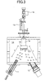
- FIG.3 shows an apparatus suitable for manufacturing a zinc oxide thin film where the oxygen plasma cell 11 and zinc crucible 12 are disposed respectively on the left and right sides as viewed in the figure without the dopant and crucible 13 in the apparatus for manufacturing a zinc oxide thin film as shown in FIG.1 .
- Solid zinc in the zinc crucible 12 is heated to high temperatures (300°C to 350°C), becomes vapor zinc (zinc atoms), and evaporates toward the substrate 101 (for example, plastic substrate) held by the substrate holder 10.
- a material of the zinc crucible is not limited particularly unless the material melts at high temperatures. In terms of high thermal conductivity and the like, preferably is a cylindrical crucible made of molybdenum with the inner surface covered with silica glass or ceramics.
- the dissociation energy necessary to decompose one oxygen molecule to two oxygen atoms is 1.4eV, resulting in the equation of O 2 +1.4eV ⁇ 2O.
- a distance (X) between the oxygen plasma cell 11 and substrate and another distance (Y) between the zinc crucible 12 and substrate are adjusted by a substrate up/down mechanism 15 so that the temperature of the substrate is not more than the desired temperature due to radiation heat.
- the mean free path is determined by the relationship with the degree of vacuum of the film-forming chamber, and it is necessary to consider the cost of the film forming apparatus, area to form a film in one processing and the like. It is possible to control the temperature of the substrate by determining the distances (X) and (Y) to meet the above-mentioned conditions.
- the substrate up/down mechanism 15 serves as such control means or a mechanism to move the substrate holder upward and downward.
- a temperature control plate may be attached that controls the effect of radiation heat.
- a material of the temperature control plate may be stainless.
- the zinc atoms and oxygen radicals reaching the substrate 101 form a zinc oxide thin film by the reaction of the zinc atom and oxygen radical as described above, while diffusing two-dimensionally on the surface of the substrate 101.
- a crystal of zinc oxide first forms a small island, and grows gradually from the island as a seed, thereby forming a zinc oxide thin film.
- the substrate is plastic as defined in claim 1, it is considered that since crystal orientations of islands generated and scattered on the substrate are different from one another, a polycrystal zinc oxide film is formed.
- a uniform zinc oxide thin film it is preferable to form the film while rotating the substrate 101 by a substrate rotating mechanism 16.
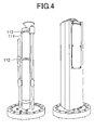
- FIG.4 illustrates an appearance of a prototyped oxygen plasma cell.
- the oxygen plasma cell is made of a silica tube of height 300 mm, inner diameter of 26 mm, outer diameter of 30 mm and thickness of 2 mm, and provided in the upper portion with twenty-one oxygen radical injecting fine holes 113 each with a diameter of 0.2 mm to inject the oxygen plasma.
- FIG.5 shows graphs illustrating simulations of electric field strength distribution and potential distribution when the distance between ring-shaped discharge electrodes is varied.
- the dielectric constant of oxygen is 1.0005
- the dielectric constant of silica is 3.8
- the dielectric loss factor is 0.0001
- the electric resistivity of copper is 1.55x10 -8 ⁇ cm
- a potential difference of 735 volts is applied between the ring-shaped electrodes 112.
- the potential and electric field strength along the center axis of the cell are as shown in FIGs. 5(a) and 5(b) , respectively.
- the maximum electric strength reaches 241 V/cm when the distance between the electrodes is 30 mm.
- the distance between the ring-shaped electrodes 112 is preferably about 30 mm in the oxygen plasma cell with the above-mentioned sizes, and the distance between discharge electrodes was set at 30 mm in the prototype apparatus.
- FIG.6 is a graph showing characteristics of emission spectrum of plasmas generated by supplying high-frequency power (13.56MHz, a potential difference between the upper and lower electrodes is 1500 V (50W)) to capacitive coupling glow discharge electrodes of the oxygen plasma cell as shown in FIG.4 .
- the degree of vacuum was 10 -6 torr in the film-forming chamber.
- strong spectra are observed at 777 nm and 844 nm, and generation of oxygen radicals was recognized.
- Illustrative Examples are not in accordance with the present invention.
- FIG.7 illustrates characteristics of zinc oxide thin films formed on glass substrates widely used as a transparent substrate.
- the films were formed while changing the temperature of the substrate to 420°C, 300°C, 150°C, 100°C, 80°C, 60°C and 40°C.
- FIG.7(a) is a photograph showing conditions of the film formed at each temperature. In the figure, numeric values in the upper right portion indicate the film forming temperature and film thickness. It has been shown that films formed at either of temperatures have sufficient transparency.
- FIG.7(b) is a graph showing light transmittance spectra for each film-forming temperature. It has been shown that the films formed at either of temperatures have a light transmittance of 80% to 90% or more in the visible region (from 380 nm to 770 nm).
- FIG.8 shows graphs illustrating relationships between the film-forming temperature and resistivity and between the film-forming temperature and carrier density. It has been understood from FIG.8(a) that the resistivity decreases as the film-forming temperature decreases, and from FIG.8(b) that the carrier density increases as the film-forming temperature decreases. From the aforementioned facts, a result was obtained that the carrier density ranging from 1x10 20 to 5x10 21 carriers/cm 3 is necessary to obtain the low resistivity of 1x10 -3 ⁇ cm or less in film-forming temperatures less than or equal to 100°C.
- the zinc atom and oxygen atom are boned one-to-one.
- a defect occurs in the zinc oxide crystal of zinc oxide. Defects generated in a zinc excessive state (oxygen shortage state) act as carrier sources, and are rather preferable for the conductive film.
- FIG.9 shows graphs illustrating relationships between the resistivity or carrier density on the vertical axis and the number (arbitrary unit) of bonded zinc atoms, on the horizontal axis, which are not bonded with oxygen measured by x-ray excited photo-electron spectroscopy. It is understood from FIG.9(b) that the carrier density increases as the lattice defect increases. Further, it is understood from FIG.9(a) that the resistivity decreases as the lattice defect increases.
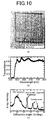
- FIG. 10 illustrates characteristics of the zinc oxide thin film formed on a PET (Polyethylene terephthalate) substrate.
- the zinc oxide thin film with a thickness of 550 nm was formed with the temperature of the substrate set at 50°C.
- FIG. 10(a) is a photograph of the formed film, and as can be seen from the figure, the film shows sufficient transparency.
- FIG.10(b) is a graph showing the spectrum of light transmittance, and it has been shown that the light transmittance is 80% ormore in the visible region.
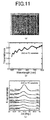
- FIG. 11 illustrates characteristics of the zinc oxide thin film formed on a PC (Polycarbonate) substrate.
- the zinc oxide thin film with a thickness of 910 nm was formed with the temperature of the substrate set at 60°C.
- FIG.11(a) is a photograph of the formed film, and as can be seen from the figure, the film shows sufficient transparency.
- FIG.11(b) is a graph showing the spectrum of light transmittance, and it has been shown that the light transmittance is 60% to 80% or more in the visible region.
- One of reasons why the transmittance is low at around 400 nm is the thickness, and it is considered that the transmittance of 80% or more is obtained in about half such a thickness.
- FIG.12 illustrates characteristics of zinc oxide thin films formed on PVC (Polyvinyl chloride) substrates. The films were formed while setting the temperature of the substrate at 50°C, 60°C and 70°C. As can be seen from FIG.12(a) , excellent transparency was obtained in the films formed at either of temperatures.
- PVC Polyvinyl chloride
- FIG. 13 illustrates characteristics of the zinc oxide thin film formed on a PP (Polypropylene) substrate.
- the film was formed with the temperature of the substrate set at 50°C.
- FIG. 13(a) there is not a significant difference in transparency between the PP substrate with the zinc oxide thin film formed thereon (upper photograph) and PP itself (lower photograph). Accordingly, it was recognized that excellent transparency is obtained in the film formed with the temperature of the substrate set at 50°C.
- FIG.13(b) is a graph showing the X-raydiffraction spectrum of the zinc oxide thin film.
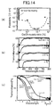
- FIG. 14 shows a graph illustrating the relationship between the supply ratio of gallium to zinc and resistivity of the zinc oxide thin film formed with gallium as a dopant and other graphs.
- FIG.14(a) shows the relationship between the supply ratio of gallium to zinc and resistivity when gallium was added to the dopant crucible 13 as a dopant, the temperature of gallium was controlled to between 730°C and 800°C by controlling the temperature of the dopant crucible 13, and the supply ratio of gallium to zinc was thereby varied in forming the zinc oxide thin film.
- the temperature of the substrate was 290°C
- the temperature of zinc was 385°C
- the high-frequency power was 150 W.
- the zinc oxide thin film with low resistivity was formed when the supply ratio of gallium to zinc is about 10 -1 %.
- the number of gallium atoms at this ratio is as follows:
- FIG.15 shows graphs illustrating the relationship between the supply ratio of gallium to zinc and the carrier density and the like.
- the number of gallium in the zinc oxide thin film is 3x10 20 /cm 3 . This result is considered caused by the fact that the deposit efficiency of gallium to the substrate is ten times higher than that of zinc. Accordingly, a zinc oxide thin film with the lowest resistivity is formed when the ratio of the dopant to zinc in the zinc oxide thin film is about 1:100.
- FIG. 14(b) is a graph illustrating the relationship between the wavelength and transmittance of the zinc oxide thin film formed while varying the supply ratio of gallium to zinc.
- the supply ratio of Ga/Zn was varied in the range of 0% to 0.1%, and in any supply ratios, almost the same transmittance was obtained in the visible region.
- FIG.14(c) is a graph showing the transmittance in the infrared region.
- the film with the supply ratio of gallium to zinc of 0.1% does not allow IR rays with wavelengths of 1.5 ⁇ m or more to pass through
- the film with the supply ratio of gallium to zinc of 0.05% does not allow IR rays with wavelengths of 1.7 ⁇ m or more to pass through. From these facts, it is understood that using the zinc oxide thin film enables production of IR shielding transparent sheets, and for example, by covering a window with a zinc oxide thin film sheet produced by this method, it is made possible to block heat from the outside.
- FIG.16 shows a graph illustrating the relationship between the supply ratio of gallium to zinc and resistivity of the zinc oxide thin film formed with gallium as a dopant using glass, polyethylene terephthalate (PET), or polycarbonate (PC) as a substrate with its temperature set at low temperature (90°C) and other graphs.
- the resistivity is the lowest in zinc oxide thin films formed on PET and PC substrates in the supply ratio of gallium to zinc of about 10 -1 %.
- FIGs.16(b) and 16(c) are graphs showing the transmittance of zinc oxide thin films on glass substrates formed similarly at low temperature (90°C).
- the excellent transmittance is obtained in the visible region, and IR rays are shielded in the region more than 2.5 ⁇ m.
- the present invention it is possible to form zinc oxide thin films with low resistivity and high transparency in the visible region on flexible substrates such as plastic. It is thereby possible to substitute the zinc oxide thin film for the indium tin oxide (ITO) film conventionally used in electronic devices such as digital cameras, DVD videos, plasma display panels, organic EL panels and the like.
- ITO indium tin oxide
Landscapes
- Chemical & Material Sciences (AREA)
- Mechanical Engineering (AREA)
- Chemical Kinetics & Catalysis (AREA)
- Engineering & Computer Science (AREA)
- Materials Engineering (AREA)
- Metallurgy (AREA)
- Organic Chemistry (AREA)
- General Chemical & Material Sciences (AREA)
- Inorganic Chemistry (AREA)
- Physical Vapour Deposition (AREA)
- Manufacturing Of Electric Cables (AREA)
- Inorganic Compounds Of Heavy Metals (AREA)
- Glass Compositions (AREA)
Abstract
Description
- The present invention relates to a method for manufacturing a zinc oxide thin film at low temperatures.
- Transparent electrode films are indispensable to electronic components of a digital camera, DVD video, plasma display panel, organic EL panel and the like, and ITO (Indium Tin Oxide) films have been used widely in the transparent electrode films. However, Indium is expensive, further has the problem of resource exhaustion, and needs to be urgently replaced with another material.
- Zinc oxide is chemically stable and conventionally used harmless material, and has an advantage of low environmental load. Among principal methods of manufacturing a thin film of zinc oxide are sputtering, organic metal chemical vapor deposition (CVD), and spray thermal decomposition method. Sputtering has been used the most widely, but has problems that the film has nonuniform electric resistivity and that the nonuniformity is remarkable when the film is formed at low temperatures.
- Organic metal CVD has problems of generating a large mount of waste gas and imposing heavy loads on the environment. Problems of the spray thermal decomposition method are that heat of about 550°C is necessary to obtain the high-performance film and that the film cannot be formed at low temperatures.
- Another technique to form a zinc oxide thin film other than the above-mentioned methods is Molecular Beam Epitaxy (MBE) (see "Plasma assisted MBE growth and characterization of hexagonal ZnO on GaAs (1111)" Proceeding of 1st Asia-Pacific Workshop on Widegap Semiconductors, 153-156 (2003) and "MBE growth and optical properties of ZnO on GaAs (1111) substrates" Phys. Stat. sol. (b), 241, 591-594(2004)). However, formation of zinc oxide thin film disclosed in the these documents is to form the film at temperatures of 400°C or more, and a problem arises that these methods cannot be applied to the case of using materials with low heat resistance such as plastic as a substrate. Another problem is that doping impurities is necessary to form the film to decrease the electric resistivity of the transparent electrode film.
- Further,
Japanese Patent Application Publication Nos.:2003-89875 JP 2001-271167 - Furthermore, in the method of forming a zinc oxide thin film disclosed in these documents and the like, a substrate placed in a film-forming chamber evacuated to a vacuum is heated to 400°C or more to accelerate the zinc oxide reaction and the film is thereby formed. Moreover, these methods do not provide sufficient conductivity, and have the need of doping impurities during formation of the film.
- Nakahara et al., "Growth and Characterization of Undoped ZnO Films for Single Crystal Based Device Use by Radical Source Molecular Beam Epitaxy", Journal of Crystal Growth, Elsevier, Amsterdam, vol. 227-228, 2001, pp. 923-928, relates to the production of undoped ZnO films by radical source molecular beam epitaxy. A ZnO buffer layer is grown on a sapphire substrate at 350°C and a ZnO film is grown on the buffer layer at higher temperatures.
-
EP-A-1081256 discloses a ZnO crystal growing methods comprising the steps of: - growing a low temperature growth ZnO layer on a sapphire substrate at a temperature lower than a single crystal growth ZnO growth temperature;
- thermally processing the low temperature growth ZnO layer with a temperature near to a growth temperature of a high temperature growth single crystal ZnO layer higher than the growth temperature of the low temperature growth ZnO layer; and
- growing a high temperature growth single crystal ZnO layer on the low temperature growth ZnO layer at a temperature higher than the growth temperature of the low temperature growth ZnO layer.
- K. Hat subara et. al. disclose in Thin Solid Films 422 (2002) 176-179 a study on Room Temperature deposition of Al-doped ZnO films by oxygen radical assisted pulsed laser deposition.
- It is a principal obj ect of the present invention to provide a method of forming a zinc oxide thin film with high transparency and high conductivity on a surface of a flexible substrate such as plastic without the indispensable requirement of doping impurities, and further provide a display and the like using the thin film.
- As a result of long-time research, the inventor of the present invention obtained new findings that when oxygen radicals react with zinc atoms at low temperatures, the regularity of the atomic arrangement of zinc oxide deteriorates, and as a result, visible light scatted by crystal defect portions to degrade the transparency, however, by controlling the crystal defect density to a predetermined density or less when the regularity of the atomic arrangement of zinc oxide deteriorates, the transparency is guaranteed in the visible region.
- Further, by intentionally disturbing the regularity of the atomic arrangement of a zinc oxide thin film, the crystal defects can be used as carrier sources, and it is made possible to generate a large number of carriers from the carrier sources. Thus, new findings were obtained that it is possible to form a zinc oxide thin film with high conductivity without doping impurities, while ensuring the transparency.
- In the present invention, in a method of forming a zinc oxide thin film by reacting oxygen radicals and zinc atoms on a surface of a substrate placed in a film-forming chamber evacuated to a vacuum, the density of crystal defects that are defects of the atomic arrangement of the zinc oxide thin film is controlled by the temperature of the substrate, and the zinc oxide thin film is thereby formed. The crystal defects are mainly of oxygen holes.
- Accordingly the present invention provides the subject matter as defined in the claims.
- It is preferable to control the temperature of the substrate by adjusting the distance between an oxygen radical source and the substrate and/or the distance between a zinc atom source and the substrate and/or the distance between a dopant source and the substrate. It is possible to control the temperature of the substrate by suppressing the effect of radiation heat of the oxygen radical source and zinc atom source and dopant source.
- In the case of using as an oxygen radical source an oxygen plasma cell system of generating plasmas in a silica or alumina or sapphire tube filled with oxygen, generating oxygen radicals from the oxygen plasma cell, and supplying the oxygen radicals to a substrate, the temperature of the silica tube is about 350°C or more at minimum, and needs to be 400°C or more to increase the oxygen supply amount. As a result, the substrate is heated to 400°C or more by radiation heat depending on conditions. However, by maintaining the distance between the oxygen plasma cell and substrate at a predetermined distance or more, it is possible to suppress the effect of radiation heat from the oxygen plasma cell and prevent increases in temperature of the substrate.
- Further, in the case of using a system of vaporizing solid zinc to supply zinc atoms to a substrate, a zinc crucible used in evaporating solid zinc needs to be heated to temperatures of at least 300°C or more, and to increase the supply amount of zinc atoms, to be heated to 400°C or more. Therefore, by controlling the distance between the zinc crucible and substrate, it is possible to control the effect of radiation heat from the zinc crucible. In other words, it is suitable to control the effect of radiation heat from the oxygen plasma cell and zinc crucible and dopant crucible by adjusting respective distances with the substrate.
- It is suitable that the distance between the substrate and the oxygen radical source or zinc atom source is a mean free path or less of an oxygen radical or zinc atom, respectively. When the distance is set that enables the effects of radiation heat from the oxygen radical source and zinc atom source on the substrate to be adjusted to the desired temperature or less, if the distance is longer than the mean free path, part of the oxygen radicals and/or zinc atoms looses the energy before reaching the substrate, and cannot arrive at the surface of the substrate. Further, even when reaching the surface, such radicals and/or atoms degrade the reaction on the surface of the substrate. Therefore, it is preferable to set the distance that enables the effects of radiation heat to be adjusted to within a desired range and that is less than or equal to the mean free path.
- It is suitable to control the temperature of the substrate to the desired temperature by forcefully cooling means. For example, it is preferable to dispose a pipe around and/or in a substrate holder, circulate water through the pipe to cool the substrate and control the temperature of the substrate.
- As another method of intentionally disturbing the regularity of the atomic arrangement of the zinc oxide thin film, it is preferable to control a supply amount of the oxygen radical and/or zinc atom to the substrate, and thereby control the density of crystal defects that are defects of the atomic arrangement of the zinc oxide thin film. By supplying a larger supply amount of the zinc atom than that of the oxygen radical to the surface of the substrate, or supplying a smaller supply amount of the oxygen radical than that of the zinc atom to the surface of the substrate, the reaction lacks oxygen. It is thereby possible to control the concentration of crystal defects.
- By controlling the crystal defects to within the range of 1x10¹⁸ defects/cm3 to 5x10²¹ defects/cm3, it is possible to provide the electric resistivity of 1x10⁻⁴ Ωcm or less and the visible light transmittance of 80% or more. In addition, in the case where the high transmittance is not required, for example, in electro-magnetic shielding material and the like, the zinc oxide thin film with high conductivity may be formed by setting the density of crystal defects at 5x10²¹ defects/cm3 or more.
- It is suitable to control the ratio between the oxygen radical supplied from the oxygen radical source and zinc atoms supplied from the zinc oxide source reacting on the surface of the substrate. On the surface of the substrate, when unreacted zinc atoms are deposited to the substrate during the reaction expressed by Zn (Zinc atom)+O* (Oxygen radical)→ZnO, the crystal defect (lattice defect) arises. By adjusting the ratio between the supply amount of the zinc atom and the supply amount of the oxygen radical, it is possible to control the density of crystal defects. It is thereby possible to form the zinc oxide thin film with high conductivity without doping the impurity. The supply amounts of the zinc atom and the oxygen radical can be controlled by controlling the temperature of the zinc crucible and the exciting power of oxygen plasma cell or adjusting the capacity of the zinc crucible and oxygen plasma cell, respectively.
- The method as defined herein may be carried out using a zinc oxide thin film manufacturing apparatus comprising a film-forming chamber evacuated to a vacuum, an oxygen plasma cell that is disposed in the film-forming chamber and that is provided with fine holes to inject oxygen radicals, a zinc crucible that is disposed in the film-forming chamber and that generates vapor of zinc atoms, a dopant crucible that is disposed in the film-forming chamber and that generates vapor of dopant atoms, and a substrate holder that is disposed in the film-forming chamber and that holds a substrate with a surface on which a zinc oxide thin film is formed by reaction of the oxygen radicals and the zinc atoms, where the distance between the substrate and an oxygen radical source and/or the distance between the substrate and a zinc atom source is respectively set at a mean free path or less of the oxygen radical or zinc atom, and that means is provided for holding an effect of radiation heat from the oxygen radical source and/or the zinc atom source to under the softening point of the material of the substrate.
- It is a feature providing temperature controlling means for controlling the temperature of the substrate holder to under the softening point of the material of the substrate. By providing the substrate holder with the temperature controlling means, the temperature of the substrate can be controlled freely and readily, and it is thus possible to adjust the reaction rate of the zinc oxide thin film. As a result, it is possible to generate lattice defects caused by the supplied oxygen radicals and zinc atoms and zinc atoms remaining unreacted, and to control the density of lattice defects.
- The oxygen plasma cell and/or zinc crucible is preferably provided with a radiation plate to control the effect of radiation heat from the oxygen plasma cell or zinc crucible on the substrate, respectively.
- The oxygen plasma cell is preferably of capacitive coupling type ring-shaped electrodes. By using the capacitive coupling type ring-shaped electrodes, it is possible to facilitate generation of plasma than in ICP (Inductive coupling plasma). For example, providing the ring-shaped electrodes outside the oxygen plasma cell facilitates adjustment of intensity of plasma generation and maintenance and thus is preferable.
- According to the present invention, it is possible to form a transparent zinc oxide thin film with high transmittance and high conductivity on a surface of a flexible substrate as defined in
claim 1 without the indispensable requirement of doping impurities. Further, it is possible to form a zinc oxide thin film at high speed without using a complicated apparatus. - The above and other objects and features of the invention will appear more fully hereinafter from a consideration of the following description taken in connection with the accompanying drawing wherein one example is illustrated by way of example, in which;
-
FIG.1 is a view showing an entire apparatus suitable for manufacturing a zinc oxide thin film; -
FIG.2 is a detail view of an oxygen plasma cell; -
FIG.3 is a detail view of the apparatus suitable for manufacturing a zinc oxide thin film with a film-forming chamber centered; -
FIG. 4 is a view of an appearance of the oxygen plasma cell prototyped in Example 1; -
FIG.5 shows graphs illustrating simulations of electric field strength distribution and potential distribution when the distance between ring-shaped discharge electrodes is varied; -
FIG.6 is a graph showing characteristics of emission spectrum of plasmas generated by supplying high-frequency power (13.56MHz, upper electrode of +500V, lower electrode of -500V) to the capacitive coupling discharge electrodes of the oxygen plasma cell; -
FIG.7 illustrates characteristics of zinc oxide thin films formed on glass substrates widely used as a transparent substrate; -
FIG.8 shows graphs illustrating relationships between the film-forming temperature and resistivity and between the film-forming temperature and carrier density; -
FIG.9 shows graphs illustrating relationships between the resistivity or carrier density on the vertical axis and the number (arbitrary unit) of bonded zinc atoms that are not bonded with oxygen measured by x-ray excited electron spectroscopy; -
FIG.10 illustrates characteristics of the zinc oxide thin film formed on a PET (polyethylene terephthalate) substrate; -
FIG.11 illustrates characteristics of the zinc oxide thin film formed on a PC (polycarbonate) substrate; -
FIG.12 illustrates characteristics of the zinc oxide thin film formed on a PVC (polyvinyl chloride) substrate; -
FIG.13 illustrates characteristics of the zinc oxide thin film formed on a PP (polypropylene) substrate; -
FIG.14 shows a graph illustrating the relationship between the supply ratio of gallium to zinc and the resistivity of the zinc oxide thin film formed with gallium as a dopant and other graphs; -
FIG.15 shows a graph illustrating the relationship between the supply ratio of gallium to zinc and the carrier density and other graphs; and -
FIG.16 shows a graph illustrating the relationship between the supply ratio of gallium to zinc and the resistivity of the zinc oxide thin film formed with gallium as a dopant using glass, polyethylene terephthalate (PET), or polycarbonate (PC) as a substrate with its temperature set at low temperature (90°C) and other graphs. - An embodiment of the present invention will specifically be described below with reference to accompanying drawings.
FIG.1 is a view showing an entire apparatus suitable for manufacturing a zinc oxide thin film. - The apparatus for manufacturing a zinc oxide
thin film 1 is basically comprised of a film-forming chamber 1A,substrate holder 10,oxygen plasma cell 11, andzinc crucible 12. In the case of aiming at improving the conductivity of a zinc oxide thin film, a dopant (impurities), for example, aluminum, gallium, indium, chlorine or the like is placed in adopant crucible 13, and evaporated to be doped in forming the zinc oxide thin film. - The film-forming chamber 1A is held at a vacuum by a vacuum pump. The degree of vacuum is ideally ultrahigh vacuum 1.3 x 10⁻⁸ Pa (10-10 torr), but there is a problem that the cost of the apparatus increases in proportion to an increase in the degree of vacuum. Therefore, the degree of vacuum may be determined by relationships between the mean free path of the oxygen radical and a distance between the
oxygen plasma cell 11 and thesubstrate 101 and between the mean free path of the zinc atom and a distance between thezinc crucible 12 and thesubstrate 101. The pressure is set at 1.3 x 10⁻³ Pa (10-5 torr) or less in this embodiment. Details will be described later. - Oxygen gas is provided to the
oxygen plasma cell 11 from anoxygen cylinder 20 at pressure between about 2600 to 26000 Pa (20 and 200 torr) via a flow-rate controller.Plasma space 11A inside theoxygen plasma cell 11 becomes a glow discharge state by the energy supplied from the high-frequency power supply. In theplasma space 11A, the oxygen gas supplied from theoxygen cylinder 20 becomes oxygen radicals (O*) and oxygen ions (O+) generated in the oxygen plasma, and when passed through fine holes provided in an injection opening, the oxygen ions (O+) become oxygen radicals (O*) with the oxygen radicals (O*) not changed, whereby the oxygen radicals are injected to the direction of thesubstrate 101. In addition, the degree of vacuum inside theplasma space 11A is basically determined according to Paschen's law, and suitably, about 1.3 to 0.13 Pa (10-2 to 10-3 torr). -
FIG.2 is a detail view of theoxygen plasma cell 11. To generate oxygen radicals, theoxygen plasma cell 11 is held at the degree of vacuum of about 133 to 1.3 x 10⁴ Pa (1mm to 100mm torr), and the oxygen gas is supplied to thecell 11 from theoxygen cylinder 20 to fill thecell 11 with oxygen. A high voltage is applied to between the ring-shapedelectrodes 112 from the high-frequency power supply to generate oxygen plasmas in theplasma space 11A. The generated oxygen plasmas are injected from fine holes provided in the upper portion of theoxygen plasma cell 11 as oxygen radicals. Theoxygen plasma cell 11 is preferably a silica tube, but not limited thereto, and any materials are applicable until impurities elute by generation of the plasma. - In
FIG.2(a) , the ring-shapedelectrodes 112 are disposed around the peripheries of theoxygen plasma cell 11. For example, by applying a potential difference of 1000 volts of 13.56 MHz to between the electrodes, glow discharge is generated inside thesilica tube 111 to cause a plasma state. By providing ring-shaped glow discharge electrodes around the peripheries of thesilica tube 111, provided are features that it is possible to apply the high voltage easily to between the electrodes, and make the electric field uniform inside the plasma space. Further, there is another feature that the discharge electrodes attached outside facilitate their operation and maintenance. - ICP (Induction Coupling Plasma) has conventionally been used as an electrode to generate plasmas, but using the ring-shaped electrodes enable plasmas to be generated easily with less oxygen gas than in ICP.
- The glow discharge starts when the high voltage of about 1000 volts at 13.56 MHz is applied to between the ring-shaped
electrodes 112. By glow discharge, the oxygen gas inside the plasma space between the ring-shapedelectrodes 112 becomes plasmas such as oxygen ions, oxygen atoms of the ground state, oxygen atoms of the excited state, electrons and the like (O+, O++, O, O*, e- and the like), and oxygen radicals are ejected from the plasma space toward the film-forming chamber 1A with a higher degree of vacuum through the fine holes 113. -
FIG.2(b) shows an injection plane of oxygen radicals of theoxygen plasma cell 11. Oxygen ions (O+, O++) emit the energy to transfer from the ion state to radical state when passed through thefine holes 113, become oxygen radicals (O*), and are injected to inside the film-forming chamber. It is preferable to provide a plurality offine holes 113 to release oxygen radicals uniformly into the film-forming chamber, and a diameter of the fine holes is preferably about 0.2 mm. -
FIG.3 shows an apparatus suitable for manufacturing a zinc oxide thin film where theoxygen plasma cell 11 andzinc crucible 12 are disposed respectively on the left and right sides as viewed in the figure without the dopant andcrucible 13 in the apparatus for manufacturing a zinc oxide thin film as shown inFIG.1 . Solid zinc in thezinc crucible 12 is heated to high temperatures (300°C to 350°C), becomes vapor zinc (zinc atoms), and evaporates toward the substrate 101 (for example, plastic substrate) held by thesubstrate holder 10. A material of the zinc crucible is not limited particularly unless the material melts at high temperatures. In terms of high thermal conductivity and the like, preferably is a cylindrical crucible made of molybdenum with the inner surface covered with silica glass or ceramics. - Zinc atoms (Zn) evaporated from the
zinc crucible 12 and oxygen radicals (O*) injected from theoxygen plasma cell 11 cause reaction on thesubstrate 101 according to the equation of Zn+O*→ZnO, and the reaction is exothermic reaction. This is because enthalpy of formation to form zinc oxide from zinc atoms and oxygen atoms is -3.16eV/ZnO, and the chemical equation of 2Zn+O2→2ZnO+6.32eV holds. The dissociation energy necessary to decompose one oxygen molecule to two oxygen atoms is 1.4eV, resulting in the equation of O2+1.4eV→2O. - To form ZnO by reacting zinc atoms and oxygen atoms, above-mentioned two equations are added, resulting in an equation of 2Zn+2O→2ZnO+7.72eV, and as a result, the exothermic reaction equation of Zn+O→ZnO+3.86eV holds. By this means, although the zinc oxide thin film has conventionally been formed by heating the substrate to 400°C or more, it was first demonstrated that a zinc oxide thin film can be formed in principle without heating the substrate. Forming a zinc oxide thin film on a flexible substrate as defined in
claim 1, it is only required to hold the temperature of the substrate at under the softening point of a material of the substrate. - It is necessary to consider following respects to hold the temperature of a substrate at a desired temperature or less. One is to control increases in temperature of the
substrate 101 due to radiation heat from thezinc crucible 12 because thecrucible 12 needs to be heated to 350°C or more to evaporate zinc atoms. Another one is to control increases in temperature of thesubstrate 101 due to radiation heat from theoxygen plasma cell 11. To control these increases, a distance (X) between theoxygen plasma cell 11 and substrate and another distance (Y) between thezinc crucible 12 and substrate are adjusted by a substrate up/downmechanism 15 so that the temperature of the substrate is not more than the desired temperature due to radiation heat. - Meanwhile, it is necessary to prevent each of the oxygen radical and zinc atom from colliding with an impurity inside the film-forming chamber before reaching the substrate. Therefore, the distances (X) and (Y) both need to be less than respective mean free paths of the oxygen radical and zinc atom.
- The mean free path is determined by the relationship with the degree of vacuum of the film-forming chamber, and it is necessary to consider the cost of the film forming apparatus, area to form a film in one processing and the like. It is possible to control the temperature of the substrate by determining the distances (X) and (Y) to meet the above-mentioned conditions. The substrate up/down
mechanism 15 serves as such control means or a mechanism to move the substrate holder upward and downward. - In addition, to reduce the effect of radiation heat of the
zinc crucible 12, a temperature control plate may be attached that controls the effect of radiation heat. In this case, a material of the temperature control plate may be stainless. Further, it is suitable to provide acooling mechanism 14 that forcefully cooling thesubstrate holder 10 as means for preventing an increase in temperature of the substrate due to radiation heat. - The zinc atoms and oxygen radicals reaching the
substrate 101 form a zinc oxide thin film by the reaction of the zinc atom and oxygen radical as described above, while diffusing two-dimensionally on the surface of thesubstrate 101. As the process of forming the zinc oxide thin film, it is considered that a crystal of zinc oxide first forms a small island, and grows gradually from the island as a seed, thereby forming a zinc oxide thin film. - When the substrate is plastic as defined in
claim 1, it is considered that since crystal orientations of islands generated and scattered on the substrate are different from one another, a polycrystal zinc oxide film is formed. In addition, to form a uniform zinc oxide thin film as possible, it is preferable to form the film while rotating thesubstrate 101 by asubstrate rotating mechanism 16. -
FIG.4 illustrates an appearance of a prototyped oxygen plasma cell. The oxygen plasma cell is made of a silica tube ofheight 300 mm, inner diameter of 26 mm, outer diameter of 30 mm and thickness of 2 mm, and provided in the upper portion with twenty-one oxygen radical injectingfine holes 113 each with a diameter of 0.2 mm to inject the oxygen plasma. -
FIG.5 shows graphs illustrating simulations of electric field strength distribution and potential distribution when the distance between ring-shaped discharge electrodes is varied. In addition, as physical properties used in the simulations, the dielectric constant of oxygen is 1.0005, the dielectric constant of silica is 3.8, the dielectric loss factor is 0.0001, the electric resistivity of copper is 1.55x10⁻⁸ Ωcm, and a potential difference of 735 volts is applied between the ring-shapedelectrodes 112. - The potential and electric field strength along the center axis of the cell are as shown in
FIGs. 5(a) and 5(b) , respectively. The maximum electric strength reaches 241 V/cm when the distance between the electrodes is 30 mm. As a result, it was found that the distance between the ring-shapedelectrodes 112 is preferably about 30 mm in the oxygen plasma cell with the above-mentioned sizes, and the distance between discharge electrodes was set at 30 mm in the prototype apparatus. -
FIG.6 is a graph showing characteristics of emission spectrum of plasmas generated by supplying high-frequency power (13.56MHz, a potential difference between the upper and lower electrodes is 1500 V (50W)) to capacitive coupling glow discharge electrodes of the oxygen plasma cell as shown inFIG.4 . The degree of vacuum was 10-6 torr in the film-forming chamber. As shown inFIG.6 , strong spectra are observed at 777 nm and 844 nm, and generation of oxygen radicals was recognized. Illustrative Examples are not in accordance with the present invention. -
FIG.7 illustrates characteristics of zinc oxide thin films formed on glass substrates widely used as a transparent substrate. The films were formed while changing the temperature of the substrate to 420°C, 300°C, 150°C, 100°C, 80°C, 60°C and 40°C.FIG.7(a) is a photograph showing conditions of the film formed at each temperature. In the figure, numeric values in the upper right portion indicate the film forming temperature and film thickness. It has been shown that films formed at either of temperatures have sufficient transparency. -
FIG.7(b) is a graph showing light transmittance spectra for each film-forming temperature. It has been shown that the films formed at either of temperatures have a light transmittance of 80% to 90% or more in the visible region (from 380 nm to 770 nm). -
FIG.7(c) is a graph showing X-ray diffraction spectra of zinc oxide thin films. As shown inFIG.7(c) , the formed thin films have the ZnO(0002) diffraction peak at nearly 2θ=34.5 degrees, and it was recognized that the formed thin films are zinc oxide. -
FIG.8 shows graphs illustrating relationships between the film-forming temperature and resistivity and between the film-forming temperature and carrier density. It has been understood fromFIG.8(a) that the resistivity decreases as the film-forming temperature decreases, and fromFIG.8(b) that the carrier density increases as the film-forming temperature decreases. From the aforementioned facts, a result was obtained that the carrier density ranging from 1x10²⁰ to 5x10²¹ carriers/cm3 is necessary to obtain the low resistivity of 1x10⁻³ Ωcm or less in film-forming temperatures less than or equal to 100°C. - In the zinc oxide crystal of zinc oxide, the zinc atom and oxygen atom are boned one-to-one. When the ratio deviates from this rate, a defect occurs. Defects generated in a zinc excessive state (oxygen shortage state) act as carrier sources, and are rather preferable for the conductive film.
-
FIG.9 shows graphs illustrating relationships between the resistivity or carrier density on the vertical axis and the number (arbitrary unit) of bonded zinc atoms, on the horizontal axis, which are not bonded with oxygen measured by x-ray excited photo-electron spectroscopy. It is understood fromFIG.9(b) that the carrier density increases as the lattice defect increases. Further, it is understood fromFIG.9(a) that the resistivity decreases as the lattice defect increases. - From the foregoing, it is considered that a large number of defects caused by shortage of oxygen exist on the ZnO crystal of the film formed at low temperatures, and that the defects supply carriers and decrease the resistivity of the ZnO film. Meanwhile, it was recognized that the density of defects generated in the film-forming conditions exemplified herein is not so large to degrade the transmittance of visible light, and that by adjusting the ratio between the zinc atom and oxygen radical to supply to the surface of the substrate in forming the film, it is possible to further decrease the resistivity while maintaining the high transmittance of visible light.
-
FIG. 10 illustrates characteristics of the zinc oxide thin film formed on a PET (Polyethylene terephthalate) substrate. The zinc oxide thin film with a thickness of 550 nm was formed with the temperature of the substrate set at 50°C.FIG. 10(a) is a photograph of the formed film, and as can be seen from the figure, the film shows sufficient transparency. -
FIG.10(b) is a graph showing the spectrum of light transmittance, and it has been shown that the light transmittance is 80% ormore in the visible region.FIG. 10(c) is a graph showing the X-ray diffraction spectrum of the zinc oxide thin film. As shown inFIG. 10(c) , the formed thin film has the ZnO(0002) diffraction peak at nearly 2θ=34.5 degrees, and it was recognized that the formed thin film is zinc oxide. -
FIG. 11 illustrates characteristics of the zinc oxide thin film formed on a PC (Polycarbonate) substrate. The zinc oxide thin film with a thickness of 910 nm was formed with the temperature of the substrate set at 60°C.FIG.11(a) is a photograph of the formed film, and as can be seen from the figure, the film shows sufficient transparency. -
FIG.11(b) is a graph showing the spectrum of light transmittance, and it has been shown that the light transmittance is 60% to 80% or more in the visible region. One of reasons why the transmittance is low at around 400 nm is the thickness, and it is considered that the transmittance of 80% or more is obtained in about half such a thickness.FIG.11(c) is a graph showing X-ray diffraction spectra of the zinc oxide thin film. As shown inFIG.11(c) , the formed thin film has the ZnO(0002) diffraction peak at nearly 2θ=34.5 degrees, and it was recognized that the formed thin film is zinc oxide. -
FIG.12 illustrates characteristics of zinc oxide thin films formed on PVC (Polyvinyl chloride) substrates. The films were formed while setting the temperature of the substrate at 50°C, 60°C and 70°C. As can be seen fromFIG.12(a) , excellent transparency was obtained in the films formed at either of temperatures. -
FIG.12(b) is a graph showing X-ray diffraction spectra of the zinc oxide thin films. As shown inFIG. 12(b) , the formed thin films have the ZnO(0002) diffraction peak at nearly 2θ=34.5 degrees, and it was recognized that the formed thin films are zinc oxide. -
FIG. 13 illustrates characteristics of the zinc oxide thin film formed on a PP (Polypropylene) substrate. The film was formed with the temperature of the substrate set at 50°C. As can be seen fromFIG. 13(a) , there is not a significant difference in transparency between the PP substrate with the zinc oxide thin film formed thereon (upper photograph) and PP itself (lower photograph). Accordingly, it was recognized that excellent transparency is obtained in the film formed with the temperature of the substrate set at 50°C. - Further,
FIG.13(b) is a graph showing the X-raydiffraction spectrum of the zinc oxide thin film. As shown inFIG.13(b) , the formed thin film has the ZnO(0002) diffraction peak at nearly 2θ=34.5 degrees, and it was recognized that the formed thin film is zinc oxide. -
FIG. 14 shows a graph illustrating the relationship between the supply ratio of gallium to zinc and resistivity of the zinc oxide thin film formed with gallium as a dopant and other graphs.FIG.14(a) shows the relationship between the supply ratio of gallium to zinc and resistivity when gallium was added to thedopant crucible 13 as a dopant, the temperature of gallium was controlled to between 730°C and 800°C by controlling the temperature of thedopant crucible 13, and the supply ratio of gallium to zinc was thereby varied in forming the zinc oxide thin film. At this time, the temperature of the substrate was 290°C, the temperature of zinc was 385°C, and the high-frequency power was 150 W. - As shown in
FIG.14(a) , the zinc oxide thin film with low resistivity was formed when the supply ratio of gallium to zinc is about 10-1%. The number of gallium atoms at this ratio is as follows: - The number of zinc is 4x10²² (Zn=4x10²²) per cubic centimeter of zinc oxide (ZnO). When gallium (Ga) is supplied with the supply amount of 0.1% relative to zinc, since the density of zinc oxide is 5.47g/cm3, the atomic weight of zinc is 65.39, the atomic weight of oxygen is 15.99, and the atomic weight of gallium is 69.72, the ratio is 65.39:15.99=Mzn: (5.47-Mzn), and Mzn =4.4 grams. Therefore, the number of zinc atoms is 4.4x(6x1023)/65.39=4x1022/cm3. The weight of gallium is 4.9x10⁻³ (=MGA) grams. The number of gallium atoms is (4.4x10-3)x(6x1023)/69.72=4x1019/cm3.
-
FIG.15 shows graphs illustrating the relationship between the supply ratio of gallium to zinc and the carrier density and the like. InFIG.15(a) , when considering that one carrier is generated from one gallium atom, from the carrier density at the gallium/zinc supply ratio that maximizes the mobility, the number of gallium in the zinc oxide thin film is 3x10²⁰/cm3. This result is considered caused by the fact that the deposit efficiency of gallium to the substrate is ten times higher than that of zinc. Accordingly, a zinc oxide thin film with the lowest resistivity is formed when the ratio of the dopant to zinc in the zinc oxide thin film is about 1:100. -
FIG. 14(b) is a graph illustrating the relationship between the wavelength and transmittance of the zinc oxide thin film formed while varying the supply ratio of gallium to zinc. The supply ratio of Ga/Zn was varied in the range of 0% to 0.1%, and in any supply ratios, almost the same transmittance was obtained in the visible region. -
FIG.14(c) is a graph showing the transmittance in the infrared region. As shown in the figure, it was recognized that the film with the supply ratio of gallium to zinc of 0.1% does not allow IR rays with wavelengths of 1.5 µm or more to pass through, and the film with the supply ratio of gallium to zinc of 0.05% does not allow IR rays with wavelengths of 1.7 µm or more to pass through. From these facts, it is understood that using the zinc oxide thin film enables production of IR shielding transparent sheets, and for example, by covering a window with a zinc oxide thin film sheet produced by this method, it is made possible to block heat from the outside. -
FIG.16 shows a graph illustrating the relationship between the supply ratio of gallium to zinc and resistivity of the zinc oxide thin film formed with gallium as a dopant using glass, polyethylene terephthalate (PET), or polycarbonate (PC) as a substrate with its temperature set at low temperature (90°C) and other graphs. As shown inFIG.16(a) , the resistivity is the lowest in zinc oxide thin films formed on PET and PC substrates in the supply ratio of gallium to zinc of about 10-1%.FIGs.16(b) and 16(c) are graphs showing the transmittance of zinc oxide thin films on glass substrates formed similarly at low temperature (90°C). As shown inFIG.16(b) , the excellent transmittance is obtained in the visible region, and IR rays are shielded in the region more than 2.5 µm. - According to the present invention, it is possible to form zinc oxide thin films with low resistivity and high transparency in the visible region on flexible substrates such as plastic. It is thereby possible to substitute the zinc oxide thin film for the indium tin oxide (ITO) film conventionally used in electronic devices such as digital cameras, DVD videos, plasma display panels, organic EL panels and the like.
Claims (6)
- A method of manufacturing a zinc oxide thin film without doping impurities by reacting oxygen radicals and zinc atoms on a surface of a substrate placed in a film-forming chamber evacuated to a vacuum, wherein
the density of crystal defects that are defects of the atomic arrangement of the zinc oxide thin film is controlled by at least a temperature of the substrate, and the zinc oxide thin film is formed,
the density of crystal defects is controlled to within a range of 1×10¹⁸ defects/cm3 to 5×10²¹ defects/cm3,
wherein the substrate is a flexible substrate selected from the group consisting of polycarbonate (PC), polyvinyl chloride (PVC) and polypropylene (PP),
wherein the supply amount of the oxygen radicals and zinc atoms to the substrate are controlled, wherein a zinc crucible is used to supply zinc atoms; and
wherein the temperature of the substrate is held under softening point of the material of the substrate to form the zinc oxide thin film. - The method of manufacturing a zinc oxide thin film according to claim 1, wherein the temperature of the substrate is controlled by controlling a distance between an oxygen radical source and the substrate and/or a distance between a zinc oxide source and the substrate.
- The method of manufacturing a zinc oxide thin film according to claim 2, wherein the distance between the oxygen radical source and the substrate and/or the distance between the zinc oxide source and the substrate is a mean free path or less of the oxygen radicals or the zinc oxides, respectively, and is a distance enabling an effect of radiation heat from the oxygen radical source and/or the zinc oxide source to be held at a desired temperature or less.
- An electrode including the zinc oxide thin film obtainable by the method according to claim 1.
- A flexible film, an organic or inorganic EL display, a liquid crystal display, a plasma display, a solar battery including the zinc oxide thin film obtainable by the method according to claim 1.
- An electromagnetic shielding material or infrared shielding sheet including the zinc oxide thin film obtainable by the method according to claim 1.
Applications Claiming Priority (1)
| Application Number | Priority Date | Filing Date | Title |
|---|---|---|---|
| JP2005237141 | 2005-08-18 |
Publications (2)
| Publication Number | Publication Date |
|---|---|
| EP1755154A1 EP1755154A1 (en) | 2007-02-21 |
| EP1755154B1 true EP1755154B1 (en) | 2011-02-16 |
Family
ID=36581936
Family Applications (1)
| Application Number | Title | Priority Date | Filing Date |
|---|---|---|---|
| EP06005550A Expired - Lifetime EP1755154B1 (en) | 2005-08-18 | 2006-03-17 | Method for manufacturing a zinc oxide thin film at low temperatures |
Country Status (7)
| Country | Link |
|---|---|
| US (1) | US7744965B2 (en) |
| EP (1) | EP1755154B1 (en) |
| JP (1) | JP5396579B2 (en) |
| KR (1) | KR20080037716A (en) |
| AT (1) | ATE498902T1 (en) |
| DE (1) | DE602006020093D1 (en) |
| WO (1) | WO2007020729A1 (en) |
Families Citing this family (12)
| Publication number | Priority date | Publication date | Assignee | Title |
|---|---|---|---|---|
| JP4296523B2 (en) * | 2007-09-28 | 2009-07-15 | 勝 堀 | Plasma generator |
| US8147599B2 (en) | 2009-02-17 | 2012-04-03 | Mcalister Technologies, Llc | Apparatuses and methods for storing and/or filtering a substance |
| KR101384404B1 (en) * | 2011-05-13 | 2014-04-10 | 강원대학교산학협력단 | Method for producing ZnO nanosheets |
| US9534296B2 (en) * | 2013-03-15 | 2017-01-03 | Mcalister Technologies, Llc | Methods of manufacture of engineered materials and devices |
| US9079489B2 (en) | 2013-05-29 | 2015-07-14 | Mcalister Technologies, Llc | Methods for fuel tank recycling and net hydrogen fuel and carbon goods production along with associated apparatus and systems |
| JP6306437B2 (en) * | 2014-05-31 | 2018-04-04 | 国立大学法人山梨大学 | Vertical deposition system |
| JP7314181B2 (en) | 2018-06-07 | 2023-07-25 | シランナ・ユー・ブイ・テクノロジーズ・プライベート・リミテッド | Method and material deposition system for forming semiconductor layers |
| CN109402566B (en) * | 2018-12-18 | 2021-03-26 | 深圳先进技术研究院 | A two-step method for preparing flexible vanadium oxide thin films |
| US11512389B2 (en) | 2019-03-20 | 2022-11-29 | Samsung Electronincs Co., Ltd. | Apparatus for and method of manufacturing semiconductor device |
| GB201913533D0 (en) * | 2019-09-19 | 2019-11-06 | Univ Southampton | Optical thin films and fabrication thereof |
| KR102336228B1 (en) * | 2020-04-06 | 2021-12-09 | 티오에스주식회사 | Epi-growth apparatus of separate chamber type |
| CN116479398B (en) * | 2023-04-28 | 2025-08-15 | 深圳市金鑫丰利珠宝首饰有限公司 | Diamond film and preparation method thereof |
Family Cites Families (21)
| Publication number | Priority date | Publication date | Assignee | Title |
|---|---|---|---|---|
| JPS61132902A (en) * | 1984-11-30 | 1986-06-20 | Osaka Tokushu Gokin Kk | Transparent film for blocking ultraviolet ray and infrared ray |
| JP2696874B2 (en) | 1988-02-04 | 1998-01-14 | 株式会社ブリヂストン | Heat shielding material and heat shielding glass |
| US5811050A (en) * | 1994-06-06 | 1998-09-22 | Gabower; John F. | Electromagnetic interference shield for electronic devices |
| US6110544A (en) * | 1997-06-26 | 2000-08-29 | General Electric Company | Protective coating by high rate arc plasma deposition |
| JP3424814B2 (en) * | 1999-08-31 | 2003-07-07 | スタンレー電気株式会社 | ZnO crystal structure and semiconductor device using the same |
| JP3953238B2 (en) * | 1999-09-01 | 2007-08-08 | 独立行政法人科学技術振興機構 | Ferromagnetic p-type single crystal zinc oxide and method for producing the same |
| JP2001271167A (en) | 2000-03-24 | 2001-10-02 | Okura Ind Co Ltd | Method of forming zinc oxide thin film |
| JP2002020884A (en) * | 2000-07-04 | 2002-01-23 | Canon Inc | Zinc oxide laminated thin film body and method of manufacturing the same |
| JP3904378B2 (en) * | 2000-08-02 | 2007-04-11 | ローム株式会社 | Zinc oxide transparent conductive film |
| WO2002016679A1 (en) * | 2000-08-18 | 2002-02-28 | Tohoku Techno Arch Co., Ltd. | Polycrystalline semiconductor material and method of manufacture thereof |
| JP4447756B2 (en) | 2000-08-28 | 2010-04-07 | 独立行政法人産業技術総合研究所 | Radical cell device and method for producing II-VI compound semiconductor device |
| JP4540201B2 (en) * | 2000-09-13 | 2010-09-08 | 独立行政法人産業技術総合研究所 | Method for manufacturing semiconductor device having ZnO-based oxide semiconductor layer |
| FR2818009B1 (en) * | 2000-12-07 | 2003-03-28 | Teherani Ferechteh Hosseini | PROCESS FOR PRODUCING A PROHIBITED BROADBAND SEMICONDUCTOR |
| JP2003089875A (en) | 2001-09-14 | 2003-03-28 | Okura Ind Co Ltd | Method of forming zinc oxide thin film |
| JP2003316276A (en) * | 2002-02-25 | 2003-11-07 | Matsushita Electric Ind Co Ltd | Impact-resistant film for flat display panel and flat display panel |
| EP1339082A1 (en) | 2002-02-25 | 2003-08-27 | Asahi Glass Company Ltd. | Impact-resistant film for flat display panel, and flat display panel |
| JP3849012B2 (en) | 2002-03-04 | 2006-11-22 | 独立行政法人物質・材料研究機構 | Low pressure low temperature vapor phase synthesis method of zinc oxide thin film |
| JP4268405B2 (en) * | 2002-12-20 | 2009-05-27 | スタンレー電気株式会社 | ZnO crystal growth method, ZnO crystal structure, and semiconductor device using the same |
| JP4252809B2 (en) * | 2003-01-15 | 2009-04-08 | スタンレー電気株式会社 | Method for producing ZnO crystal and method for producing ZnO-based LED |
| JP2005237141A (en) | 2004-02-20 | 2005-09-02 | Toyota Motor Corp | Inverter and method for manufacturing inverter |
| JP5291928B2 (en) * | 2007-12-26 | 2013-09-18 | 株式会社日立製作所 | Oxide semiconductor device and manufacturing method thereof |
-
2006
- 2006-03-16 WO PCT/JP2006/305244 patent/WO2007020729A1/en not_active Ceased
- 2006-03-16 JP JP2007530913A patent/JP5396579B2/en not_active Expired - Lifetime
- 2006-03-16 KR KR1020087006448A patent/KR20080037716A/en not_active Ceased
- 2006-03-17 US US11/377,204 patent/US7744965B2/en active Active
- 2006-03-17 AT AT06005550T patent/ATE498902T1/en not_active IP Right Cessation
- 2006-03-17 EP EP06005550A patent/EP1755154B1/en not_active Expired - Lifetime
- 2006-03-17 DE DE602006020093T patent/DE602006020093D1/en not_active Expired - Lifetime
Non-Patent Citations (1)
| Title |
|---|
| PAVLIK J. ET AL: "Study of argon/oxygen plasma used for creation of aluminium oxide thin film", SUPERFICIES Y VACIO, vol. 9, December 1999 (1999-12-01), MEXICO, pages 131 - 134 * |
Also Published As
| Publication number | Publication date |
|---|---|
| ATE498902T1 (en) | 2011-03-15 |
| JPWO2007020729A1 (en) | 2009-02-19 |
| US20070042216A1 (en) | 2007-02-22 |
| DE602006020093D1 (en) | 2011-03-31 |
| EP1755154A1 (en) | 2007-02-21 |
| US7744965B2 (en) | 2010-06-29 |
| WO2007020729A1 (en) | 2007-02-22 |
| KR20080037716A (en) | 2008-04-30 |
| JP5396579B2 (en) | 2014-01-22 |
Similar Documents
| Publication | Publication Date | Title |
|---|---|---|
| Jayathilake et al. | Overview on transparent conducting oxides and state of the art of low-cost doped ZnO systems | |
| TWI435943B (en) | Thin film metal oxynitride semiconductor | |
| US7744965B2 (en) | Method and apparatus for manufacturing a zinc oxide thin film at low temperatures | |
| Seong et al. | Enhanced uniformity in electrical and optical properties of ITO thin films using a wide thermal annealing system | |
| US20110049715A1 (en) | Method for depositing metal oxide films | |
| KR102732452B1 (en) | Method for forming transition metal dichalcogenide film and method of manufacturing an electric device including the same | |
| Gan et al. | High carrier mobility tungsten-doped indium oxide films prepared by reactive plasma deposition in pure argon and post annealing | |
| Colibaba | Sintering highly conductive ZnO: HCl ceramics by means of chemical vapor transport reactions | |
| Wang et al. | ZnO thin film grown on silicon by metal-organic chemical vapor deposition | |
| US20150345010A1 (en) | Methods of magnetically enhanced physical vapor deposition | |
| US20120090546A1 (en) | Source supplying unit, method for supplying source, and thin film depositing apparatus | |
| US9856578B2 (en) | Methods of producing large grain or single crystal films | |
| Hymavathi et al. | Influence of sputtering power on structural, electrical and optical properties of reactive magnetron sputtered Cr doped CdO thin films | |
| KR102385038B1 (en) | Apparatus for growing single crystal metal-oxide epi wafer | |
| JP2012132090A (en) | Method for forming electrically conductive transparent zinc oxide-based film, electrically conductive transparent zinc oxide-based film, and elecrically conductive transparent substrate | |
| Weng et al. | Structure, optical and electrical properties of ZnO thin films on the flexible substrate by cathodic vacuum arc technology with different arc currents | |
| Sahoo et al. | Band gap variation in copper nitride thin films | |
| Terai et al. | Structural and luminescent properties of Er-doped ZnO films grown by metalorganic chemical vapor deposition | |
| Cho et al. | Highly conductive air-stable ZnO thin film formation under in situ UV illumination for an indium-free transparent electrode | |
| JP2008223123A (en) | Radical generator | |
| KR100594383B1 (en) | Method of manufacturing zinc oxide thin film doped with aluminum | |
| US20140144770A1 (en) | Method of fabricating zinc oxide thin film | |
| JP2008255444A (en) | SUBSTRATES WITH ZnCuSe THIN FILM, AND ITS MANUFACTURING METHOD | |
| Takikawa et al. | Cathodic arc deposition with activated anode (CADAA) for preparation of in situ doped thin solid films | |
| RU2769751C1 (en) | Device for deposition of ultra-thick layers of polycrystalline silicon |
Legal Events
| Date | Code | Title | Description |
|---|---|---|---|
| PUAI | Public reference made under article 153(3) epc to a published international application that has entered the european phase |
Free format text: ORIGINAL CODE: 0009012 |
|
| AK | Designated contracting states |
Kind code of ref document: A1 Designated state(s): AT BE BG CH CY CZ DE DK EE ES FI FR GB GR HU IE IS IT LI LT LU LV MC NL PL PT RO SE SI SK TR |
|
| AX | Request for extension of the european patent |
Extension state: AL BA HR MK YU |
|
| 17P | Request for examination filed |
Effective date: 20070821 |
|
| AKX | Designation fees paid |
Designated state(s): AT BE BG CH CY CZ DE DK EE ES FI FR GB GR HU IE IS IT LI LT LU LV MC NL PL PT RO SE SI SK TR |
|
| 17Q | First examination report despatched |
Effective date: 20071121 |
|
| RAP1 | Party data changed (applicant data changed or rights of an application transferred) |
Owner name: UNIVERSITY OF YAMANASHI Owner name: YAMANASHI PREFECTURE Owner name: NAKAYA LTD |
|
| RTI1 | Title (correction) |
Free format text: METHOD FOR MANUFACTURING A ZINC OXIDE THIN FILM AT LOW TEMPERATURES |
|
| GRAP | Despatch of communication of intention to grant a patent |
Free format text: ORIGINAL CODE: EPIDOSNIGR1 |
|
| GRAS | Grant fee paid |
Free format text: ORIGINAL CODE: EPIDOSNIGR3 |
|
| GRAA | (expected) grant |
Free format text: ORIGINAL CODE: 0009210 |
|
| AK | Designated contracting states |
Kind code of ref document: B1 Designated state(s): AT BE BG CH CY CZ DE DK EE ES FI FR GB GR HU IE IS IT LI LT LU LV MC NL PL PT RO SE SI SK TR |
|
| REG | Reference to a national code |
Ref country code: GB Ref legal event code: FG4D |
|
| REG | Reference to a national code |
Ref country code: CH Ref legal event code: EP |
|
| REG | Reference to a national code |
Ref country code: IE Ref legal event code: FG4D |
|
| REF | Corresponds to: |
Ref document number: 602006020093 Country of ref document: DE Date of ref document: 20110331 Kind code of ref document: P |
|
| REG | Reference to a national code |
Ref country code: DE Ref legal event code: R096 Ref document number: 602006020093 Country of ref document: DE Effective date: 20110331 |
|
| REG | Reference to a national code |
Ref country code: NL Ref legal event code: VDEP Effective date: 20110216 |
|
| LTIE | Lt: invalidation of european patent or patent extension |
Effective date: 20110216 |
|
| PG25 | Lapsed in a contracting state [announced via postgrant information from national office to epo] |
Ref country code: SE Free format text: LAPSE BECAUSE OF FAILURE TO SUBMIT A TRANSLATION OF THE DESCRIPTION OR TO PAY THE FEE WITHIN THE PRESCRIBED TIME-LIMIT Effective date: 20110216 Ref country code: GR Free format text: LAPSE BECAUSE OF FAILURE TO SUBMIT A TRANSLATION OF THE DESCRIPTION OR TO PAY THE FEE WITHIN THE PRESCRIBED TIME-LIMIT Effective date: 20110517 Ref country code: LT Free format text: LAPSE BECAUSE OF FAILURE TO SUBMIT A TRANSLATION OF THE DESCRIPTION OR TO PAY THE FEE WITHIN THE PRESCRIBED TIME-LIMIT Effective date: 20110216 Ref country code: PT Free format text: LAPSE BECAUSE OF FAILURE TO SUBMIT A TRANSLATION OF THE DESCRIPTION OR TO PAY THE FEE WITHIN THE PRESCRIBED TIME-LIMIT Effective date: 20110616 Ref country code: LV Free format text: LAPSE BECAUSE OF FAILURE TO SUBMIT A TRANSLATION OF THE DESCRIPTION OR TO PAY THE FEE WITHIN THE PRESCRIBED TIME-LIMIT Effective date: 20110216 Ref country code: ES Free format text: LAPSE BECAUSE OF FAILURE TO SUBMIT A TRANSLATION OF THE DESCRIPTION OR TO PAY THE FEE WITHIN THE PRESCRIBED TIME-LIMIT Effective date: 20110527 |
|
| PG25 | Lapsed in a contracting state [announced via postgrant information from national office to epo] |
Ref country code: BE Free format text: LAPSE BECAUSE OF FAILURE TO SUBMIT A TRANSLATION OF THE DESCRIPTION OR TO PAY THE FEE WITHIN THE PRESCRIBED TIME-LIMIT Effective date: 20110216 Ref country code: BG Free format text: LAPSE BECAUSE OF FAILURE TO SUBMIT A TRANSLATION OF THE DESCRIPTION OR TO PAY THE FEE WITHIN THE PRESCRIBED TIME-LIMIT Effective date: 20110516 Ref country code: SI Free format text: LAPSE BECAUSE OF FAILURE TO SUBMIT A TRANSLATION OF THE DESCRIPTION OR TO PAY THE FEE WITHIN THE PRESCRIBED TIME-LIMIT Effective date: 20110216 Ref country code: NL Free format text: LAPSE BECAUSE OF FAILURE TO SUBMIT A TRANSLATION OF THE DESCRIPTION OR TO PAY THE FEE WITHIN THE PRESCRIBED TIME-LIMIT Effective date: 20110216 Ref country code: PL Free format text: LAPSE BECAUSE OF FAILURE TO SUBMIT A TRANSLATION OF THE DESCRIPTION OR TO PAY THE FEE WITHIN THE PRESCRIBED TIME-LIMIT Effective date: 20110216 Ref country code: FI Free format text: LAPSE BECAUSE OF FAILURE TO SUBMIT A TRANSLATION OF THE DESCRIPTION OR TO PAY THE FEE WITHIN THE PRESCRIBED TIME-LIMIT Effective date: 20110216 Ref country code: CY Free format text: LAPSE BECAUSE OF FAILURE TO SUBMIT A TRANSLATION OF THE DESCRIPTION OR TO PAY THE FEE WITHIN THE PRESCRIBED TIME-LIMIT Effective date: 20110216 Ref country code: AT Free format text: LAPSE BECAUSE OF FAILURE TO SUBMIT A TRANSLATION OF THE DESCRIPTION OR TO PAY THE FEE WITHIN THE PRESCRIBED TIME-LIMIT Effective date: 20110216 |
|
| PG25 | Lapsed in a contracting state [announced via postgrant information from national office to epo] |
Ref country code: DK Free format text: LAPSE BECAUSE OF FAILURE TO SUBMIT A TRANSLATION OF THE DESCRIPTION OR TO PAY THE FEE WITHIN THE PRESCRIBED TIME-LIMIT Effective date: 20110216 Ref country code: EE Free format text: LAPSE BECAUSE OF FAILURE TO SUBMIT A TRANSLATION OF THE DESCRIPTION OR TO PAY THE FEE WITHIN THE PRESCRIBED TIME-LIMIT Effective date: 20110216 Ref country code: MC Free format text: LAPSE BECAUSE OF NON-PAYMENT OF DUE FEES Effective date: 20110331 |
|
| REG | Reference to a national code |
Ref country code: CH Ref legal event code: PL |
|
| PG25 | Lapsed in a contracting state [announced via postgrant information from national office to epo] |
Ref country code: RO Free format text: LAPSE BECAUSE OF FAILURE TO SUBMIT A TRANSLATION OF THE DESCRIPTION OR TO PAY THE FEE WITHIN THE PRESCRIBED TIME-LIMIT Effective date: 20110216 Ref country code: CZ Free format text: LAPSE BECAUSE OF FAILURE TO SUBMIT A TRANSLATION OF THE DESCRIPTION OR TO PAY THE FEE WITHIN THE PRESCRIBED TIME-LIMIT Effective date: 20110216 Ref country code: SK Free format text: LAPSE BECAUSE OF FAILURE TO SUBMIT A TRANSLATION OF THE DESCRIPTION OR TO PAY THE FEE WITHIN THE PRESCRIBED TIME-LIMIT Effective date: 20110216 |
|
| PLBE | No opposition filed within time limit |
Free format text: ORIGINAL CODE: 0009261 |
|
| STAA | Information on the status of an ep patent application or granted ep patent |
Free format text: STATUS: NO OPPOSITION FILED WITHIN TIME LIMIT |
|
| REG | Reference to a national code |
Ref country code: IE Ref legal event code: MM4A |
|
| 26N | No opposition filed |
Effective date: 20111117 |
|
| PG25 | Lapsed in a contracting state [announced via postgrant information from national office to epo] |
Ref country code: CH Free format text: LAPSE BECAUSE OF NON-PAYMENT OF DUE FEES Effective date: 20110331 Ref country code: IE Free format text: LAPSE BECAUSE OF NON-PAYMENT OF DUE FEES Effective date: 20110317 Ref country code: LI Free format text: LAPSE BECAUSE OF NON-PAYMENT OF DUE FEES Effective date: 20110331 |
|
| REG | Reference to a national code |
Ref country code: DE Ref legal event code: R097 Ref document number: 602006020093 Country of ref document: DE Effective date: 20111117 |
|
| PG25 | Lapsed in a contracting state [announced via postgrant information from national office to epo] |
Ref country code: IT Free format text: LAPSE BECAUSE OF FAILURE TO SUBMIT A TRANSLATION OF THE DESCRIPTION OR TO PAY THE FEE WITHIN THE PRESCRIBED TIME-LIMIT Effective date: 20110216 |
|
| PG25 | Lapsed in a contracting state [announced via postgrant information from national office to epo] |
Ref country code: LU Free format text: LAPSE BECAUSE OF NON-PAYMENT OF DUE FEES Effective date: 20110317 |
|
| PG25 | Lapsed in a contracting state [announced via postgrant information from national office to epo] |
Ref country code: IS Free format text: LAPSE BECAUSE OF FAILURE TO SUBMIT A TRANSLATION OF THE DESCRIPTION OR TO PAY THE FEE WITHIN THE PRESCRIBED TIME-LIMIT Effective date: 20110216 |
|
| PG25 | Lapsed in a contracting state [announced via postgrant information from national office to epo] |
Ref country code: TR Free format text: LAPSE BECAUSE OF FAILURE TO SUBMIT A TRANSLATION OF THE DESCRIPTION OR TO PAY THE FEE WITHIN THE PRESCRIBED TIME-LIMIT Effective date: 20110216 |
|
| PG25 | Lapsed in a contracting state [announced via postgrant information from national office to epo] |
Ref country code: HU Free format text: LAPSE BECAUSE OF FAILURE TO SUBMIT A TRANSLATION OF THE DESCRIPTION OR TO PAY THE FEE WITHIN THE PRESCRIBED TIME-LIMIT Effective date: 20110216 |
|
| REG | Reference to a national code |
Ref country code: FR Ref legal event code: PLFP Year of fee payment: 11 |
|
| REG | Reference to a national code |
Ref country code: FR Ref legal event code: PLFP Year of fee payment: 12 |
|
| REG | Reference to a national code |
Ref country code: FR Ref legal event code: PLFP Year of fee payment: 13 |
|
| PGFP | Annual fee paid to national office [announced via postgrant information from national office to epo] |
Ref country code: GB Payment date: 20220321 Year of fee payment: 17 Ref country code: DE Payment date: 20220324 Year of fee payment: 17 |
|
| PGFP | Annual fee paid to national office [announced via postgrant information from national office to epo] |
Ref country code: FR Payment date: 20220322 Year of fee payment: 17 |
|
| REG | Reference to a national code |
Ref country code: DE Ref legal event code: R119 Ref document number: 602006020093 Country of ref document: DE |
|
| GBPC | Gb: european patent ceased through non-payment of renewal fee |
Effective date: 20230317 |
|
| PG25 | Lapsed in a contracting state [announced via postgrant information from national office to epo] |
Ref country code: GB Free format text: LAPSE BECAUSE OF NON-PAYMENT OF DUE FEES Effective date: 20230317 |
|
| PG25 | Lapsed in a contracting state [announced via postgrant information from national office to epo] |
Ref country code: GB Free format text: LAPSE BECAUSE OF NON-PAYMENT OF DUE FEES Effective date: 20230317 Ref country code: FR Free format text: LAPSE BECAUSE OF NON-PAYMENT OF DUE FEES Effective date: 20230331 Ref country code: DE Free format text: LAPSE BECAUSE OF NON-PAYMENT OF DUE FEES Effective date: 20231003 |