EP1754981A1 - ZnO SINGLE CRYSTAL AS SUPER HIGH SPEED SCINTILLATOR AND METHOD FOR PREPARATION THEREOF - Google Patents
ZnO SINGLE CRYSTAL AS SUPER HIGH SPEED SCINTILLATOR AND METHOD FOR PREPARATION THEREOF Download PDFInfo
- Publication number
- EP1754981A1 EP1754981A1 EP05741568A EP05741568A EP1754981A1 EP 1754981 A1 EP1754981 A1 EP 1754981A1 EP 05741568 A EP05741568 A EP 05741568A EP 05741568 A EP05741568 A EP 05741568A EP 1754981 A1 EP1754981 A1 EP 1754981A1
- Authority
- EP
- European Patent Office
- Prior art keywords
- zno
- luminescence
- composition ratio
- single crystal
- scintillator
- Prior art date
- Legal status (The legal status is an assumption and is not a legal conclusion. Google has not performed a legal analysis and makes no representation as to the accuracy of the status listed.)
- Withdrawn
Links
Images







Classifications
-
- G—PHYSICS
- G21—NUCLEAR PHYSICS; NUCLEAR ENGINEERING
- G21K—HANDLING OF PARTICLES OR IONISING RADIATION NOT OTHERWISE PROVIDED FOR; IRRADIATION DEVICES; GAMMA RAY OR X-RAY MICROSCOPES
- G21K4/00—Conversion screens for the conversion of the spatial distribution of X-rays or particle radiation into visible images, e.g. fluoroscopic screens
-
- C—CHEMISTRY; METALLURGY
- C09—DYES; PAINTS; POLISHES; NATURAL RESINS; ADHESIVES; COMPOSITIONS NOT OTHERWISE PROVIDED FOR; APPLICATIONS OF MATERIALS NOT OTHERWISE PROVIDED FOR
- C09K—MATERIALS FOR MISCELLANEOUS APPLICATIONS, NOT PROVIDED FOR ELSEWHERE
- C09K11/00—Luminescent materials, e.g. electroluminescent or chemiluminescent
- C09K11/08—Luminescent materials, e.g. electroluminescent or chemiluminescent containing inorganic luminescent materials
- C09K11/56—Luminescent materials, e.g. electroluminescent or chemiluminescent containing inorganic luminescent materials containing sulfur
- C09K11/562—Chalcogenides
- C09K11/565—Chalcogenides with zinc cadmium
-
- C—CHEMISTRY; METALLURGY
- C09—DYES; PAINTS; POLISHES; NATURAL RESINS; ADHESIVES; COMPOSITIONS NOT OTHERWISE PROVIDED FOR; APPLICATIONS OF MATERIALS NOT OTHERWISE PROVIDED FOR
- C09K—MATERIALS FOR MISCELLANEOUS APPLICATIONS, NOT PROVIDED FOR ELSEWHERE
- C09K11/00—Luminescent materials, e.g. electroluminescent or chemiluminescent
- C09K11/08—Luminescent materials, e.g. electroluminescent or chemiluminescent containing inorganic luminescent materials
- C09K11/59—Luminescent materials, e.g. electroluminescent or chemiluminescent containing inorganic luminescent materials containing silicon
- C09K11/592—Chalcogenides
- C09K11/595—Chalcogenides with zinc or cadmium
-
- C—CHEMISTRY; METALLURGY
- C09—DYES; PAINTS; POLISHES; NATURAL RESINS; ADHESIVES; COMPOSITIONS NOT OTHERWISE PROVIDED FOR; APPLICATIONS OF MATERIALS NOT OTHERWISE PROVIDED FOR
- C09K—MATERIALS FOR MISCELLANEOUS APPLICATIONS, NOT PROVIDED FOR ELSEWHERE
- C09K11/00—Luminescent materials, e.g. electroluminescent or chemiluminescent
- C09K11/08—Luminescent materials, e.g. electroluminescent or chemiluminescent containing inorganic luminescent materials
- C09K11/62—Luminescent materials, e.g. electroluminescent or chemiluminescent containing inorganic luminescent materials containing gallium, indium or thallium
- C09K11/621—Chalcogenides
- C09K11/623—Chalcogenides with zinc or cadmium
-
- C—CHEMISTRY; METALLURGY
- C09—DYES; PAINTS; POLISHES; NATURAL RESINS; ADHESIVES; COMPOSITIONS NOT OTHERWISE PROVIDED FOR; APPLICATIONS OF MATERIALS NOT OTHERWISE PROVIDED FOR
- C09K—MATERIALS FOR MISCELLANEOUS APPLICATIONS, NOT PROVIDED FOR ELSEWHERE
- C09K11/00—Luminescent materials, e.g. electroluminescent or chemiluminescent
- C09K11/08—Luminescent materials, e.g. electroluminescent or chemiluminescent containing inorganic luminescent materials
- C09K11/64—Luminescent materials, e.g. electroluminescent or chemiluminescent containing inorganic luminescent materials containing aluminium
- C09K11/641—Chalcogenides
- C09K11/642—Chalcogenides with zinc or cadmium
-
- C—CHEMISTRY; METALLURGY
- C09—DYES; PAINTS; POLISHES; NATURAL RESINS; ADHESIVES; COMPOSITIONS NOT OTHERWISE PROVIDED FOR; APPLICATIONS OF MATERIALS NOT OTHERWISE PROVIDED FOR
- C09K—MATERIALS FOR MISCELLANEOUS APPLICATIONS, NOT PROVIDED FOR ELSEWHERE
- C09K11/00—Luminescent materials, e.g. electroluminescent or chemiluminescent
- C09K11/08—Luminescent materials, e.g. electroluminescent or chemiluminescent containing inorganic luminescent materials
- C09K11/66—Luminescent materials, e.g. electroluminescent or chemiluminescent containing inorganic luminescent materials containing germanium, tin or lead
- C09K11/661—Chalcogenides
- C09K11/662—Chalcogenides with zinc or cadmium
-
- C—CHEMISTRY; METALLURGY
- C09—DYES; PAINTS; POLISHES; NATURAL RESINS; ADHESIVES; COMPOSITIONS NOT OTHERWISE PROVIDED FOR; APPLICATIONS OF MATERIALS NOT OTHERWISE PROVIDED FOR
- C09K—MATERIALS FOR MISCELLANEOUS APPLICATIONS, NOT PROVIDED FOR ELSEWHERE
- C09K11/00—Luminescent materials, e.g. electroluminescent or chemiluminescent
- C09K11/08—Luminescent materials, e.g. electroluminescent or chemiluminescent containing inorganic luminescent materials
- C09K11/77—Luminescent materials, e.g. electroluminescent or chemiluminescent containing inorganic luminescent materials containing rare earth metals
- C09K11/7701—Chalogenides
- C09K11/7702—Chalogenides with zinc or cadmium
-
- C—CHEMISTRY; METALLURGY
- C30—CRYSTAL GROWTH
- C30B—SINGLE-CRYSTAL GROWTH; UNIDIRECTIONAL SOLIDIFICATION OF EUTECTIC MATERIAL OR UNIDIRECTIONAL DEMIXING OF EUTECTOID MATERIAL; REFINING BY ZONE-MELTING OF MATERIAL; PRODUCTION OF A HOMOGENEOUS POLYCRYSTALLINE MATERIAL WITH DEFINED STRUCTURE; SINGLE CRYSTALS OR HOMOGENEOUS POLYCRYSTALLINE MATERIAL WITH DEFINED STRUCTURE; AFTER-TREATMENT OF SINGLE CRYSTALS OR A HOMOGENEOUS POLYCRYSTALLINE MATERIAL WITH DEFINED STRUCTURE; APPARATUS THEREFOR
- C30B29/00—Single crystals or homogeneous polycrystalline material with defined structure characterised by the material or by their shape
- C30B29/10—Inorganic compounds or compositions
- C30B29/16—Oxides
-
- C—CHEMISTRY; METALLURGY
- C30—CRYSTAL GROWTH
- C30B—SINGLE-CRYSTAL GROWTH; UNIDIRECTIONAL SOLIDIFICATION OF EUTECTIC MATERIAL OR UNIDIRECTIONAL DEMIXING OF EUTECTOID MATERIAL; REFINING BY ZONE-MELTING OF MATERIAL; PRODUCTION OF A HOMOGENEOUS POLYCRYSTALLINE MATERIAL WITH DEFINED STRUCTURE; SINGLE CRYSTALS OR HOMOGENEOUS POLYCRYSTALLINE MATERIAL WITH DEFINED STRUCTURE; AFTER-TREATMENT OF SINGLE CRYSTALS OR A HOMOGENEOUS POLYCRYSTALLINE MATERIAL WITH DEFINED STRUCTURE; APPARATUS THEREFOR
- C30B33/00—After-treatment of single crystals or homogeneous polycrystalline material with defined structure
Definitions
- the present invention relates to a crystal to be used as a scintillator in a scintillation detector.
- Devices for measuring ionizing radiation include a scintillation detector.
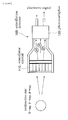
- the mechanism of a typical scintillation detector is shown in Fig. 1.
- Fig. 1 when an ionizing radiation is incident on a scintillation detector 100, fluorescence according to the incoming ionizing radiation is generated in a scintillator crystal 110, and this fluorescence is amplified by a photomultiplier 120 and detected, whereby the ionizing radiation can be measured.
- a scintillator having a fluorescence lifetime of not more than 1 ns is required for a Time-Of-Flight type PET (hereinafter referred to as TOF-PET for short) that is considered as a next-generation PET scanner.
- TOF-PET Time-Of-Flight type PET
- scintillator with different luminescence mechanism from conventional materials Ba 4 Ge 3 O 12 (BGO); ⁇ 400 ns, Ce:Lu 2 SiO 5 (Ce:LSO); ⁇ 40 ns
- Barium fluoride (BaF 2 ) is regarded as a leading candidate material for TOF-PET scanner because its fluorescence lifetime of luminescence by cross luminescence (CL) is 0.8 ns. This value is the shortest among currently known sincillators, whose bulk crystals are available to produce. However, scintillator with much shorter lifetime is desirable for the TOF-PET.
- the light yield of BaF 2 is about 10 to 20% compared with that of BGO.
- BGO is a conventional and well known scintillator material; however, it is insufficient for manufacture of a high-sensitivity PET.
- BaF2 has one more serious problem. It has luminescence with long fluorescence lifetime ( ⁇ 600 ns), which is called self-trapped exciton (STE). This luminescence prevents the detection of the luminescence from CL, since it is more intensive than the luminescence by CL.
- BaF 2 further has problems in the price as the whole device or the sensitivity, since an expensive PMT with quartz window must be used because of its short emission wavelength of 180-220 nm (general PMT cannot be used).
- BaF 2 is hygroscopic, although it is not serious magnitude. It has a tendency to be lower the quality by reaction with moisture in the air. Therefore, coating, vacuum encapsulation or usage of inert gas atmosphere is needed for its long-term use.
- the PET scanner must have high efficiency of absorbing ⁇ -ray, which is a high-energy particle beam.
- the capability of absorbing ⁇ -ray depends on the average atomic numbers of atoms constituting a crystal and the density of the crystal. The larger the value, the higher the capability. Since BaF 2 has low ⁇ -ray stopping power with a density of 4.89 g/cm 3 . This value is low as a scintillator material, therefore, a long piece is required for absorbing of ⁇ -ray, which causes reduced position resolution.
- BaF 2 is a fluoride, it forms oxy fluoride if an oxygen source is present in the growth condition.
- the raw material must be carefully prepared so as to minimize impurities of oxygen source.
- a precise atmospheric control must be performed during the production from the viewpoint of oxygen source removal, which needs special raw material treatment and crystal producing apparatus, resulting in a slightly increased price of crystal.
- An object of the present invention is to find out a new scintillator material in place of BaF 2 , and find out a method for producing this material at low cost.
- M Al, Ga, In, Y, Sc, La, Gd, Lu
- a ZnO single crystal including those doped with Al ⁇ Ga ⁇ In ⁇ Y ⁇ Sc ⁇ La ⁇ Gd ⁇ Lu ⁇ Si ⁇ Ge ⁇ Sn ⁇ Pb ⁇ Cd
- a general photomultiplier can be used.
- the ZnO crystal can be produced at low cost. This is apparent from the example of quartz.
- ZnO single crystal is generally produced by flux method, CVT method, hydrothermal method, and so on.
- those produced by the general methods include impurities (Fe, Ni, Cr, etc.) which inhibit light emission, and have high density of crystal defects, the energy excited by X-ray, ⁇ -ray or other ionizing radiation is thermally reduced or it turned to be a visible light with long decay time.
- a platinum inner container For reducing impurities in ZnO single crystal such as Fe, Ni or Cr which inhibit light emission, a platinum inner container is effective. It makes solution not to directly contact with an autoclave. As a result, LiOH and KOH can be used in appropriate quantities as a mineralizer, consequently, defects of the ZnO single crystal can be consequently reduced.
- Doping to ZnO can be performed by adding Al 2 O 3 , Ga 2 O 2 , In 2 O 3 , Y 2 O 3 , Sc 2 O 3 , La 2 O 3 , Gd 2 O 3 , Lu 2 O 3 , SiO 2 , GeO 2 , SnO 2 , PbO, CdO and so on. They are mixed with starting material or mineralizer aqueous solution. Further, the doping amount can be controlled by changing the charging amount. Further, by doping these elements, the emission wavelength is shifted to long wavelength side, resulting in the suppression of the self-absorption, and the luminescence by exciton can be efficiently taken out (detected).
- Reduction of distortion in the crystal surface which suppress the emission intensity, can be reduced by performing annealing at 1000 to 1400°C for 5 to 15 hours in oxygen atmosphere. Consequently, the excitation energy can be efficiently transformed to the luminescence center.
- the fluorescence lifetime of the luminescence by free exciton of ZnO is about 0.6 ns which is shorter than that of BaF 2 and sufficiently satisfies the value necessary for the TOF-type PET.
- the emission intensity of luminescence from ZnO which is strongly depending on the amount of impurities, can be increased by controlling the amount of impurities and the concentration of the dopant. Although luminescence with long fluorescence lifetime by impurities is present at about 500 nm, this luminescence can be also inhibited by controlling the amount of impurities.
- the luminescence from free exciton of ZnO has emission peaking around 370 nm and general PMT can be used.
- ZnO is stable in the air, and free from the problems of hygroscopicity.
- This crystal is intended to convert a radioactive ray such as ⁇ -ray or X-ray to visible light as a scintillator crystal.
- the higher density is more suitable for efficient absorption of ⁇ -ray or X-ray, and ZnO has a density of 5.61 g/cm 3 , and it has better stopping power than that of BaF 2 .
- ZnO single crystal is rather expensive. This is because it is produced by vapor-phase growth. However, now it can be grown by the hydrothermal method. This growth method is same as artificial quartz, whose is famous for economical price.
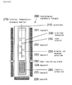
- a crystal of ZnO for scintillator which will be described in detail was produced, using a hydrothermal synthesis furnace 200 having a structure as shown in Fig. 2.
- a platinum container 230 is used as an inner cylinder in order for a solution not to directly contact with the autoclave 210.
- a seed crystal 240, a mineralizer aqueous solution 250 and a reaction precursor 260 are enclosed in the container 230.
- the mineralizer aqueous solution 250 an aqueous solution containing LiOH: 1 mol/l and KOH: 3 mol/l is used.
- ZnO can be doped by adding Al 2 O 3 , Ga 2 O 3 , In 2 O 3 , Y 2 O 3 , Sc 2 O 3 , La 2 O 3 , Gd 2 O 3 , Lu 2 O 3 , SiO 2 , GeO 2 , SnO 2 , PbO, CdO or the like to the reaction precursor 260 or the mineralizer aqueous solution 250 that is a starting material for hydrothermal synthesis.
- the doping amount is controlled by changing the charging amount (starting composition) of the doping material.
- a heater 1 211 to a heater 6 216 for heating are set on the outside of the autoclave 210.
- the platinum container 230 is partitioned by a heat insulating plate 280 to an upper part and a lower part having a temperature difference of about 20°C.
- the one melted from the reaction precursor 260 in the lower part of the platinum container 230 is crystallized in the seed crystal 240 in the upper part.
- the mineralizer aqueous solution 250 is used to promote the crystallization.
- x represents a composition ratio of (Zn 1-x M x )O 1+x (M: Al, Ga, In, Y, Sc, La, Gd, Lu) or a composition ratio of (Zn 1-x M' x )O 1+2x (M': Si, Ge, Sn, Pb) or (Zn 1-x Cd x )O.
- Fig. 3 shows X-ray rocking curve measurement data of the undoped ZnO single crystal.
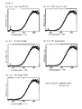
- Fig. 4 shows a luminescence emission spectrum at room temperature to UV excitation of the ZnO single crystal. It is the luminescence by exciton of the arrowed part in the drawing that is used as a scintillator. The broad peak in visible range cannot be used as the scintillator because of a long lifetime.
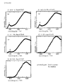
- Figs. 5 show luminescence emission spectra at room temperature to UV excitation of the Al-doped ZnO single crystals. It is also the luminescence by exciton of the arrowed part in the drawings that is used as the scintillator.
- the doping amounts of A1 are 0.1% (composition ratio 0.001) in Fig. 5(a), 0.5% (composition ratio 0.005) in Fig. 5(b), 1.0% (composition ratio 0.01) in Fig. 5(c), 5.0% (composition ratio 0.05) in Fig. 5(d), 15% (composition ratio 0.15) in Fig. 5(e), respectively.
- the luminescence by exciton was observed with Al: not more than 1.0%.
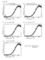
- Figs. 6 show luminescence emission spectra at room temperature to UV excitation of the Ga-doped ZnO single crystals. It is also the luminescence by exciton of the arrowed part in the drawings that is used as the scintillator.
- the doping amounts of Ga are 0.1% (composition ratio 0.001) in Fig. 6(a), 0.5% (composition ratio 0.005) in Fig. 6(b), 1.0% (composition ratio 0.01) in Fig. 6(c), 5.0% (composition ratio 0.05) in Fig. 6(d), 15% (composition ratio 0.15) in Fig. 6(e), respectively.
- the luminescence by exciton was observed with Ga: not more than 5.0%.
- Figs. 7 show luminescence emission spectra at room temperature to UV excitation of the In-doped ZnO single crystals. It is also the luminescence by exciton of the arrowed part in the drawings that is used as the scintillator.
- the doping amounts of In are 0.1% (composition ratio 0.001) in Fig. 7(a), 0.5% (composition ratio 0.005) in Fig. 7(b), 1.0% (composition ratio 0.01) in Fig. 7(c), 5.0% (composition ratio 0.05) in Fig. 7(d), 15% (composition ratio 0.15) in Fig. 7(e), respectively.
- the luminescence by exciton was observed with In: not more than 1.0%.
- Figs. 8 show luminescence emission spectra at room temperature to UV excitation of the Y-doped ZnO single crystals. It is also the luminescence by exciton of the arrowed part in the drawings that is used as the scintillator.
- the doping amounts of Y are 0.1% (composition ratio 0.001) in Fig. 8(a), 0.5% (composition ratio 0.005) in Fig. 8(b), 1.0% (composition ratio 0.01) in Fig. 8(c), 5.0% (composition ratio 0.05) in Fig. 8(d), 15% (composition ratio 0.15) in Fig. 8(e), respectively.
- the luminescence by exciton was observed with Y: not more than 1.0%.
- Figs. 9 show luminescence emission spectra at room temperature to UV excitation of the Sc-doped ZnO single crystals. It is also the luminescence by exciton of the arrowed part in the drawings that is used as the scintillator.
- the doping amounts of Sc are 0.1% (composition ratio 0.001) in Fig. 9(a), 0.5% (composition ratio 0.005) in Fig. 9(b), 1.0% (composition ratio 0.01) in Fig. 9(c), 5.0% (composition ratio 0.05) in Fig. 9(d), 15% (composition ratio 0.15) in Fig. 9(e), respectively.
- the luminescence by exciton was observed with Sc: not more than 1.0%.
- Figs. 10 show luminescence emission spectra at room temperature to UV excitation of the La-doped ZnO single crystals. It is also the luminescence by exciton of the arrowed part in the drawings that is used as the scintillator.
- the doping amounts of La are 0.1% (composition ratio 0.001) in Fig. 10(a), 0.5% (composition ratio 0.005) in Fig. 10(b), 1.0% (composition ratio 0.01) in Fig. 10(c), 5.0% (composition ratio 0.05) in Fig. 10(d), 15% (composition ratio 0.15) in Fig. 10(e), respectively.
- the luminescence by exciton was observed with La: not more than 1.0%.
- Figs. 11 show luminescence emission spectra at room temperature to UV excitation of the Gd-doped ZnO single crystals. It is also the luminescence by exciton of the arrowed part in the drawings that is used as the scintillator.
- the doping amounts of Gd are 0.1% (composition ratio 0.001) in Fig. 11(a), 0.5% (composition ratio 0.005) in Fig. 11(b), 1.0% (composition ratio 0.01) in Fig. 11(c), 5.0% (composition ratio 0.05) in Fig. 11(d), 15% (composition ratio 0.15) in Fig. 11(e), respectively.
- the luminescence by exciton was observed with Gd: not more than 1.0%.
- Figs. 12 show luminescence emission spectra at room temperature to UV excitation of the Lu-doped ZnO single crystals. It is also the luminescence by exciton of the arrowed part in the drawings that is used as the scintillator.
- the doping amounts of Lu are 0.1% (composition ratio 0.001) in Fig. 12(a), 0.5% (composition ratio 0.005) in Fig. 12(b), 1.0% (composition ratio 0.01) in Fig. 12(c), 5.0% (composition ratio 0.05) in Fig. 12(d), 15% (composition ratio 0.15) in Fig. 12(e), respectively.
- the luminescence by exciton was observed with Lu: not more than 1.0%.
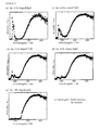
- Figs. 13 show luminescence emission spectra at room temperature to UV excitation of the Si-doped ZnO single crystals. It is also the luminescence by exciton of the arrowed part in the drawings that is used as the scintillator.
- the doping amounts of Si are 0.1% (composition ratio 0.001) in Fig. 13(a), 0.25% (composition ratio 0.0025) in Fig. 13(b), 0.5% (composition ratio 0.005) in Fig. 13(c), 2.5% (composition ratio 0.025) in Fig. 13(d), 15% (composition ratio 0.15) in Fig. 13(e), respectively.
- the luminescence by exciton was observed with Si: not more than 1.0%.
- Figs. 14 show luminescence emission spectra at room temperature to UV excitation of the Ge-doped ZnO single crystals. It is also the luminescence by exciton of the arrowed part in the drawings that is used as the scintillator.
- the doping amounts of Ge are 0.1% (composition ratio 0.001) in Fig. 14(a), 0.25% (composition ratio 0.0025) in Fig. 14(b), 0.5% (composition ratio 0.005) in Fig. 14(c), 2.5% (composition ratio 0.025) in Fig. 14(d), 15% (composition ratio 0.15) in Fig. 14(e), respectively.
- the luminescence by exciton was observed with Ge: not more than 1.0%.
- Figs. 15 show luminescence emission spectra at room temperature to UV excitation of the Sn-doped ZnO single crystals. It is also the luminescence by exciton of the arrowed part in the drawings that is used as the scintillator.
- the doping amounts of Sn are 0.1% (composition ratio 0.001) in Fig. 15(a), 0.25% (composition ratio 0.0025) in Fig. 15(b), 0.5% (composition ratio 0.005) in Fig. 15(c), 2.5% (composition ratio 0.025) in Fig. 15(d), 15% (composition ratio 0.15) in Fig. 15(e), respectively.
- the luminescence by exciton was observed with Sn: not more than 1.0%.
- Figs. 16 show luminescence emission spectra at room temperature to UV excitation of the Pb-doped ZnO single crystals. It is also the luminescence by exciton of the arrowed part in the drawings that is used as the scintillator.
- the doping amounts of Pb are 0.1% (composition ratio 0.001) in Fig. 16(a), 0.25% (composition ratio 0.0025) in Fig. 16(b), 0.5% (composition ratio 0.005) in Fig. 16(c), 2.5% (composition ratio 0.025) in Fig. 16(d), 15% (composition ratio 0.15) in Fig. 16(e), respectively.
- the luminescence by exciton was observed with Pb: not more than 1.0%.
- Figs. 17 show luminescence emission spectra at room temperature to UV excitation of the Cd-doped ZnO single crystals. It is also the luminescence by exciton of the arrowed part in the drawings that is used as the scintillator.
- the doping amounts of Cd are 0.1% (composition ratio 0.001) in Fig. 17(a), 0.5% (composition ratio 0.005) in Fig. 17(b), 1.0% (composition ratio 0.01) in Fig. 17(c), 5.0% (composition ratio 0.05) in Fig. 17(d), 15% (composition ratio 0.15) in Fig. 17(e), respectively.
- the luminescence by exciton was observed with Cd: not more than 1.0%.
- the crystals of ZnO doped with Al, Ga, In, Y, Sc, La, Gd, Lu, Si, Ge, Sn, Pb, Cd and the like by the hydrothermal synthetic method represent quick build up in addition to fluorescence lifetimes of not more than 0.6 ns far beyond those of the conventional materials such as BGO, and clear the reference of not more than 1 ns which is ideal for TOF-PET.
- these crystals are preferable from each point of density, emission amount, short fluorescence lifetime, chemical stability, and low price. Further, they have luminous wavelengths significantly closer to the long wavelength side than BaF 2 , and can be combined with a general PMT.
Landscapes
- Chemical & Material Sciences (AREA)
- Engineering & Computer Science (AREA)
- Materials Engineering (AREA)
- Organic Chemistry (AREA)
- Inorganic Chemistry (AREA)
- Metallurgy (AREA)
- Crystallography & Structural Chemistry (AREA)
- Physics & Mathematics (AREA)
- General Engineering & Computer Science (AREA)
- High Energy & Nuclear Physics (AREA)
- Luminescent Compositions (AREA)
- Crystals, And After-Treatments Of Crystals (AREA)
- Measurement Of Radiation (AREA)
Abstract
Description
- The present invention relates to a crystal to be used as a scintillator in a scintillation detector.
- Devices for measuring ionizing radiation include a scintillation detector. The mechanism of a typical scintillation detector is shown in Fig. 1. In Fig. 1, when an ionizing radiation is incident on a
scintillation detector 100, fluorescence according to the incoming ionizing radiation is generated in ascintillator crystal 110, and this fluorescence is amplified by aphotomultiplier 120 and detected, whereby the ionizing radiation can be measured. - As a candidate for next-generation medical imaging system, a Time-of-Flight (TOF) system has been proposed and investigated, focusing on fluorides. In time-resolved measurement, the resolution can be improved more as the fluorescence lifetime is shorter. Therefore, BaF2 has been considered to be the candidate. However, it has serious problems such that its small light yield and short emission wavelength and it requires an expensive photomultiplier (PMT) with quartz window. General photomultiplier (PMT) is not available for the detection of luminescence from BaF2. Each of the problems will be described.
- A scintillator having a fluorescence lifetime of not more than 1 ns is required for a Time-Of-Flight type PET (hereinafter referred to as TOF-PET for short) that is considered as a next-generation PET scanner. For this purpose, scintillator with different luminescence mechanism from conventional materials (Bi4Ge3O12 (BGO); ~400 ns, Ce:Lu2SiO5 (Ce:LSO); ~40 ns) is required. Barium fluoride (BaF2) is regarded as a leading candidate material for TOF-PET scanner because its fluorescence lifetime of luminescence by cross luminescence (CL) is 0.8 ns. This value is the shortest among currently known sincillators, whose bulk crystals are available to produce. However, scintillator with much shorter lifetime is desirable for the TOF-PET.
- The light yield of BaF2, that is a candidate material for the TOF-PET scintillator, is about 10 to 20% compared with that of BGO. BGO is a conventional and well known scintillator material; however, it is insufficient for manufacture of a high-sensitivity PET. Moreover, BaF2 has one more serious problem. It has luminescence with long fluorescence lifetime (~600 ns), which is called self-trapped exciton (STE). This luminescence prevents the detection of the luminescence from CL, since it is more intensive than the luminescence by CL.
- BaF2 further has problems in the price as the whole device or the sensitivity, since an expensive PMT with quartz window must be used because of its short emission wavelength of 180-220 nm (general PMT cannot be used).
- BaF2 is hygroscopic, although it is not serious magnitude. It has a tendency to be lower the quality by reaction with moisture in the air. Therefore, coating, vacuum encapsulation or usage of inert gas atmosphere is needed for its long-term use.
- The PET scanner must have high efficiency of absorbing γ-ray, which is a high-energy particle beam. The capability of absorbing γ-ray depends on the average atomic numbers of atoms constituting a crystal and the density of the crystal. The larger the value, the higher the capability. Since BaF2 has low γ-ray stopping power with a density of 4.89 g/cm3. This value is low as a scintillator material, therefore, a long piece is required for absorbing of γ-ray, which causes reduced position resolution.
- Since BaF2 is a fluoride, it forms oxy fluoride if an oxygen source is present in the growth condition. Thus, the raw material must be carefully prepared so as to minimize impurities of oxygen source. A precise atmospheric control must be performed during the production from the viewpoint of oxygen source removal, which needs special raw material treatment and crystal producing apparatus, resulting in a slightly increased price of crystal.
- An object of the present invention is to find out a new scintillator material in place of BaF2, and find out a method for producing this material at low cost.
- The present invention involves a scintillation detector, using a single crystal of (Zn1-xMx)O1+x (M: Al, Ga, In, Y, Sc, La, Gd, Lu) (x=0 to 0.0500), (Zn1-xM'x)O1+2x (M': Si, Ge, Sn, Pb) (x=0 to 0.0250) or (Zn1-xCdx)O (x=0 to 0.0500) as a scintillator. In this case, luminescence by exciton from the single crystal of (Zn1-xMx)O1+x (M: Al, Ga, In, Y, Sc, La, Gd, Lu) (x=0 to 0.0500), (Zn1-xM'x)O1+2x (M': Si, Ge, Sn, Pb) (x=0 to 0.0250) or (Zn1-xCdx)O (x=0 to 0.0500) is preferably used.
- A method for producing the crystal of (Zn1-xMx)O1+x (M: Al, Ga, In, Y, Sc, La, Gd, Lu) (x=0 to 0.0500), (Zn1-xM'x)O1+2x (M': Si, Ge, Sn, Pb) (x=0 to 0.0250) or (Zn1-xCdx)O (x=0 to 0.0500) is hydrothermal method with a platinum inner container in the autoclave. KOH and LiOH are used as a mineralizer. Dopant material M, M' or Cd is mixed with starting material in the mineralizer aqueous solution.
- A single crystal of (Zn1-xMx)O1+x (M: Al, Ga, In, Y, Sc, La, Gd, Lu) (x=0 to 0.0500), (Zn1-xM'x)O1+2x (M': Si, Ge, Sn, Pb) (x=0 to 0.0250) or (Zn1-xCdx)O (x=0 to 0.0500), which is produced by a hydrothermal with a platinum inner containner in the autoclave, is also involved in the present invention. KOH and LiOH are used as a mineralizer for the growth. Dopant material M, M' or Cd is mixed with starting material.
- Since a ZnO single crystal (including those doped with Al·Ga·In·Y·Sc·La·Gd·Lu·Si·Ge·Sn·Pb·Cd) as described above has a fluorescence lifetime remarkably shorter than those of conventional materials such as BaF2. Moreover, the wavelength of the resulting luminance is sufficiently long, a general photomultiplier can be used.
- In the case of ZnO powder, a raw material is inexpensive by several digits, compared with BaF2. Moreover, it is stable in the air without any special treatment.
- Further, since mass production is possible by adaptation of the hydrothermal method, the ZnO crystal can be produced at low cost. This is apparent from the example of quartz.
-
- Fig. 1 is a view showing the setup of a typical scintillation detector;
- Fig. 2 is a view showing the structure of a hydrothermal furnace;
- Fig. 3 is a view showing X-ray rocking curve measurement data of ZnO single crystal;
- Fig. 4 is a view showing an emission spectrum of ZnO single crystal at room temperature. It is excited by UV;
- Figs. 5 (a) to (e) are views showing emission spectra of Al-doped ZnO single crystals at room temperature. It is excited by UV. Doping concentration is as follows; (a) Al: 0.1%, (b) Al: 0.5%, (c) Al: 1.0%, (d) Al: 5.0%, and (e) Al: 15%;
- Figs. 6 (a) to (e) are views showing emission spectra of Ga-doped ZnO single crystals at room temperature. It is excited by UV. Doping concentration is as follows; (a) Ga: 0.1%, (b) Ga: 0.5%, (c) Ga: 1.0%, (d) Ga: 5.0%, and (e) Ga: 15%;
- Fig. 7 (a) to (e) are views showing emission spectra of In-doped ZnO single crystals at room temperature. It is excited by UV. Doping concentration is as follows; (a) In: 0.1%, (b) In: 0.5%, (c) In: 1.0%, (d) In: 5.0%, and (e) In: 15%;
- Fig. 8 (a) to (e) are views showing emission spectra of Y-doped ZnO single crystals at room temperature. It is excited by UV. Doping concentration is as follows; (a) Y: 0.1%, (b) Y: 0.5%, (c) Y: 1.0%, (d) Y: 5.0%, and (e) Y: 15%;
- Fig. 9 (a) to (e) are views showing emission spectra of Sc-doped ZnO single crystals at room temperature. It is excited by UV. Doping concentration is as follows; (a) Sc: 0.1%, (b) Sc: 0.5%, (c) Sc: 1.0%, (d) Sc: 5.0%, and (e) Sc: 15%;
- Fig. 10 (a) to (e) are views showing emission spectra of La-doped ZnO single crystals at room temperature. It is excited by UV. Doping concentration is as follows; (a) La: 0.1%, (b) La: 0.5%, (c) La: 1.0%, (d) La: 5.0%, and (e) La: 15%;
- Fig. 11 (a) to (e) are views showing luminescence emission spectra of Gd-doped ZnO single crystals at room temperature. It is excited by UV. Doping concentration is as follows; (a) Gd: 0.1%, (b) Gd: 0.5%, (c) Gd: 1.0%, (d) Gd: 5.0%, and (e) Gd: 15%;
- Fig. 12 (a) to (e) are views showing luminescence emission spectra of Lu-doped ZnO single crystals at room temperature. It is excited by UV. Doping concentration is as follows; (a) Lu: 0.1%, (b) Lu: 0.5%, (c) Lu: 1.0%, (d) Lu: 5.0%, and (e) Lu: 15%;
- Fig. 13 (a) to (e) are views showing luminescence emission spectra of Si-doped ZnO single crystals at room temperature. It is excited by UV. Doping concentration is as follows; (a) Si: 0.1%, (b) Si: 0.25%, (c) Si: 0.5%, (d) Si: 2.5%, and (e) Si: 15%;
- Fig. 14 (a) to (e) are views showing luminescence emission spectra of Ge-doped ZnO single crystals at room temperature. It is excited by UV. Doping concentration is as follows; (a) Ge: 0.1%, (b) Ge: 0.25%, (c) Ge: 0.5%, (d) Ge: 2.5%, and (e) Ge: 15%;
- Fig. 15 (a) to (e) are views showing luminescence emission spectra of Sn-doped ZnO single crystals at room temperature. It is excited by UV. Doping concentration is as follows; (a) Sn: 0.1%, (b) Sn: 0.25%, (c) Sn: 0.5%, (d) Sn: 2.5%, and (e) Sn: 15%;
- Fig. 16 (a) to (e) are views showing luminescence emission spectra of Pb-doped ZnO single crystals at room temperature. It is excited by UV. Doping concentration is as follows; (a) Pb: 0.1%, (b) Pb: 0.25%, (c) Pb: 0.5%, (d) Pb: 2.5%, and (e) Pb: 15%; and
- Fig. 17 (a) to (e) are views showing luminescence emission spectra of Cd-doped ZnO single crystals at room temperature. It is excited by UV. Doping concentration is as follows; (a) Cd: 0.1%, (b) Cd: 0.5%, (c) Cd: 1.0%, (d) Cd: 5.0%, and (e) Cd: 15%.
- In the course of studies for single crystals of ZnO, the present inventors found out that ZnO single crystals as described above are prominent as scintillator materials.
- ZnO single crystal is generally produced by flux method, CVT method, hydrothermal method, and so on. However, since those produced by the general methods include impurities (Fe, Ni, Cr, etc.) which inhibit light emission, and have high density of crystal defects, the energy excited by X-ray, γ-ray or other ionizing radiation is thermally reduced or it turned to be a visible light with long decay time.
- In the growth of ZnO single crystal by a conventional hydrothermal method, only the increase in quality of the crystal was focused, and a dissimilar element small doping method has not been established. Further, there is no mechanism for efficient light emission, capable of preventing absorption of precious luminescence by exciton by itself (self-absorption) in undoped ZnO which is caused by overlapping of the absorption wavelength band of ZnO itself with the wavelength of the luminescence by exciton. Further, most of the luminescence by exciton is trapped by crystal defects, and thermally reduced or it turned to be a visible light with long decay time.
- The inventors found out that a single crystal of ZnO can be produced by hydrothermal method using the Pt container. It reduces the impurities, and therefore, doping can be also possible, as described below.
- For reducing impurities in ZnO single crystal such as Fe, Ni or Cr which inhibit light emission, a platinum inner container is effective. It makes solution not to directly contact with an autoclave. As a result, LiOH and KOH can be used in appropriate quantities as a mineralizer, consequently, defects of the ZnO single crystal can be consequently reduced.
- Doping to ZnO can be performed by adding Al2O3, Ga2O2, In2O3, Y2O3, Sc2O3, La2O3, Gd2O3, Lu2O3, SiO2, GeO2, SnO2, PbO, CdO and so on. They are mixed with starting material or mineralizer aqueous solution. Further, the doping amount can be controlled by changing the charging amount. Further, by doping these elements, the emission wavelength is shifted to long wavelength side, resulting in the suppression of the self-absorption, and the luminescence by exciton can be efficiently taken out (detected).
- Reduction of distortion in the crystal surface, which suppress the emission intensity, can be reduced by performing annealing at 1000 to 1400°C for 5 to 15 hours in oxygen atmosphere. Consequently, the excitation energy can be efficiently transformed to the luminescence center.
- The fluorescence lifetime of the luminescence by free exciton of ZnO is about 0.6 ns which is shorter than that of BaF2 and sufficiently satisfies the value necessary for the TOF-type PET.
- The emission intensity of luminescence from ZnO, which is strongly depending on the amount of impurities, can be increased by controlling the amount of impurities and the concentration of the dopant. Although luminescence with long fluorescence lifetime by impurities is present at about 500 nm, this luminescence can be also inhibited by controlling the amount of impurities.
- The luminescence from free exciton of ZnO has emission peaking around 370 nm and general PMT can be used.
- As it is oxide, ZnO is stable in the air, and free from the problems of hygroscopicity.
- This crystal is intended to convert a radioactive ray such as γ-ray or X-ray to visible light as a scintillator crystal. The higher density is more suitable for efficient absorption of γ-ray or X-ray, and ZnO has a density of 5.61 g/cm3, and it has better stopping power than that of BaF2.
- At this moment, ZnO single crystal is rather expensive. This is because it is produced by vapor-phase growth. However, now it can be grown by the hydrothermal method. This growth method is same as artificial quartz, whose is famous for economical price.
- The use of the single crystal or doped crystals of ZnO produced by the above-mentioned method as a scintillator leads to the following effects.
- 1. The amount of impurities is reduced by using a platinum liner and using KOH and LiOH as a mineralizer in the growth of ZnO single crystal by the hydrothermal synthetic method.
- 2. A dissimilar element doping method by hydrothermal synthetic method is established for efficiently taking out the luminescence by exciton from the ZnO single crystal.
- 3. The fluorescence lifetime of the luminescence by free exciton of ZnO is extremely short as about 0.6 ns, which sufficiently satisfies the value necessary for the scintillator crystal for TOF-type PET.
- 4. The light yield equal to that of BGO which is a conventional material can be attained by controlling the amount of impurities in the ZnO single crystal and the carrier doping amount by the hydrothermal synthetic method of the present invention. Luminescence by impurities having a peak at about 500 nm is reduced by reducing the amount of impurities and improving the crystallinity, and the emission amount at the vicinity of 370 nm with short fluorescence lifetime can be successfully increased.
- 5. The emission wavelength of the luminescence by free exciton of ZnO is about 370 nm, and a general PMT can be used.
- 6. ZnO is stable in the air because it is an oxide, and free from problems such as deliquescence.
- 7. This crystal is intended to convert an ionizing radiation such as γ-ray or X-ray to visible light as a scintillator crystal. The higher density is desirable for efficient absorption of γ-ray or X-ray, and ZnO has a density of 5.61 g/cm3, and is excellent in γ-ray and X-ray stopping power, compared with BaF2.
- 8. At this moment, ZnO single crystal is rather expensive. This is because it is produced by vapor-phase growth. However, now it can be grown by the hydrothermal method. This growth method is same as artificial quartz, whose is famous for economical price.
- A crystal of ZnO for scintillator which will be described in detail was produced, using a
hydrothermal synthesis furnace 200 having a structure as shown in Fig. 2. Within anautoclave 210 that is a pressure vessel, for reducing the impurities of ZnO single crystal and for precluding the impurities such as Fe, Ni or Cr, which prevents light emission, aplatinum container 230 is used as an inner cylinder in order for a solution not to directly contact with theautoclave 210. A seed crystal 240, a mineralizeraqueous solution 250 and areaction precursor 260 are enclosed in thecontainer 230. As the mineralizeraqueous solution 250, an aqueous solution containing LiOH: 1 mol/l and KOH: 3 mol/l is used. In doping, ZnO can be doped by adding Al2O3, Ga2O3, In2O3, Y2O3, Sc2O3, La2O3, Gd2O3, Lu2O3, SiO2, GeO2, SnO2, PbO, CdO or the like to thereaction precursor 260 or the mineralizeraqueous solution 250 that is a starting material for hydrothermal synthesis. The doping amount is controlled by changing the charging amount (starting composition) of the doping material. - A
heater 1 211 to a heater 6 216 for heating are set on the outside of theautoclave 210. Theplatinum container 230 is partitioned by a heat insulating plate 280 to an upper part and a lower part having a temperature difference of about 20°C. The one melted from thereaction precursor 260 in the lower part of theplatinum container 230 is crystallized in the seed crystal 240 in the upper part. The mineralizeraqueous solution 250 is used to promote the crystallization. - The growing condition of the ZnO crystal formed in the hydrothermal
synthetic furnace 200 is shown in Tables 1(a), 1(b), and 1(c). In the tables, x represents a composition ratio of (Zn1-xMx)O1+x (M: Al, Ga, In, Y, Sc, La, Gd, Lu) or a composition ratio of (Zn1-xM'x)O1+2x (M': Si, Ge, Sn, Pb) or (Zn1-xCdx)O.Table 1(a) Compound Composition (Starting Composition) Starting Material Growing Temperature (lower part, upper part) Growing Pressure Container Material ZnO ZnO (4N) 400°C, 380°C
90MPa
PtAl:ZnO ZnO (4N)
Al2O3 (5N)400°C, 380°C
90MPa
Ptx= 0.001 (0.1%) 0.005 (0.5%) 0.01 (1%) 0.05 (5%) 0.15 (15%) Ga:ZnO ZnO (4N)
Ga2O3 (4N)400°C, 380°C
90MPa
Ptx= 0.001 (0.1%) 0.005 (0.5%) 0.01 (1%) 0.05 (5%) 0.15 (15%) In:ZnO ZnO (4N)
Zn2O3 (5N)400°C, 380°C
90MPa
Ptx= 0.001 (0.1%) 0.005 (0.5%) 0.01 (1%) 0.05 (5%) 0.15 (15%) Y:ZnO ZnO (4N)
Y2O3 (5N)400°C, 380°C
90MPa
Ptx= 0.001 (0.1%) 0.005 (0.5%) 0.01 (1%) 0.05 (5%) 0.15 (15%) Sc:ZnO ZnO (4N)
Sc2O3 (5N)400°C, 380°C
90MPa
Ptx= 0.001 (0.1%) 0.005 (0.5%) 0.01 (1%) 0.05 (5%) 0.15 (15%) Table 1(b) Compound Composition (Starting Composition) Starting Material Growing Temperature (lower part, upper part) Growing Pressure Container Material La:ZnO ZnO (4N)
La2O3 (5N)400°C, 380°C
90MPa
Ptx= 0.001 (0.1%) 0.005 (0.5%) 0.01 (1%) 0.05 (5%) 0.15 (15%) Gd:ZnO ZnO (4N)
Gd2O3 (5N)400°C, 380°C
90MPa
Ptx= 0.001 (0.1%) 0.005 (0.5%) 0.01 (1%) 0.05 (5%) 0.15 (15%) Lu:ZnO ZnO (4N)
Lu2O3 (5N)400°C, 380°C
90MPa
Ptx= 0.001 (0.1%) 0.005 (0.5%) 0.01 (1%) 0.05 (5%) 0.15 (15%) Si:ZnO ZnO (4N)
SiO2 (5N)400°C, 380°C
90MPa
Ptx= 0.001 (0.1%) 0.0025 (0.25%) 0.01 (0.5%) 0.05 (2.5%) 0.15 (15%) Table 1(c) Compound Composition (Starting Composition) Starting Material Growing Temperature (lower part, upper part) Growing Pressure Container Material Ge:ZnO ZnO (4N)
GeO2 (5N)400°C, 380°C
90MPa
Ptx= 0.001 (0.1%) 0.0025 (0.25%) 0.01 (0.5%) 0.05 (2.5%) 0.15 (15%) Sn:ZnO ZnO (4N)
SnO2 (5N)400°C, 380°C
90MPa
Ptx= 0.001 (0.1%) 0.0025 (0.25%) 0.01 (0.5%) 0.05 (2.5%) 0.15 (15%) Pb:ZnO ZnO (4N)
PbO (5N)400°C, 380°C
90MPa
Ptx= 0.001 (0.1%) 0.0025 (0.25%) 0.01 (0.5%) 0.05 (2.5%) 0.15 (15%) Cd:ZnO ZnO (4N)
CdO (4N)400°C, 380°C
90MPa
Ptx= 0.001 (0.1%) 0.0025 (0.25%) 0.01 (1%) 0.05 (5%) 0.15 (15%) - Fig. 3 shows X-ray rocking curve measurement data of the undoped ZnO single crystal. As is apparent therefrom, the ZnO single crystal formed in the above-mentioned growing condition for hydrothermal synthetic method has extremely high crystallinity with minimized crystalline defects.
- Fig. 4 shows a luminescence emission spectrum at room temperature to UV excitation of the ZnO single crystal. It is the luminescence by exciton of the arrowed part in the drawing that is used as a scintillator. The broad peak in visible range cannot be used as the scintillator because of a long lifetime.
- Figs. 5 show luminescence emission spectra at room temperature to UV excitation of the Al-doped ZnO single crystals. It is also the luminescence by exciton of the arrowed part in the drawings that is used as the scintillator.
- The doping amounts of A1 are 0.1% (composition ratio 0.001) in Fig. 5(a), 0.5% (composition ratio 0.005) in Fig. 5(b), 1.0% (composition ratio 0.01) in Fig. 5(c), 5.0% (composition ratio 0.05) in Fig. 5(d), 15% (composition ratio 0.15) in Fig. 5(e), respectively. As is apparent from these drawings, the luminescence by exciton was observed with Al: not more than 1.0%.
- Figs. 6 show luminescence emission spectra at room temperature to UV excitation of the Ga-doped ZnO single crystals. It is also the luminescence by exciton of the arrowed part in the drawings that is used as the scintillator.
- The doping amounts of Ga are 0.1% (composition ratio 0.001) in Fig. 6(a), 0.5% (composition ratio 0.005) in Fig. 6(b), 1.0% (composition ratio 0.01) in Fig. 6(c), 5.0% (composition ratio 0.05) in Fig. 6(d), 15% (composition ratio 0.15) in Fig. 6(e), respectively. As is apparent from these drawings, the luminescence by exciton was observed with Ga: not more than 5.0%.
- Figs. 7 show luminescence emission spectra at room temperature to UV excitation of the In-doped ZnO single crystals. It is also the luminescence by exciton of the arrowed part in the drawings that is used as the scintillator.
- The doping amounts of In are 0.1% (composition ratio 0.001) in Fig. 7(a), 0.5% (composition ratio 0.005) in Fig. 7(b), 1.0% (composition ratio 0.01) in Fig. 7(c), 5.0% (composition ratio 0.05) in Fig. 7(d), 15% (composition ratio 0.15) in Fig. 7(e), respectively. As is apparent from these drawings, the luminescence by exciton was observed with In: not more than 1.0%.
- Figs. 8 show luminescence emission spectra at room temperature to UV excitation of the Y-doped ZnO single crystals. It is also the luminescence by exciton of the arrowed part in the drawings that is used as the scintillator.
- The doping amounts of Y are 0.1% (composition ratio 0.001) in Fig. 8(a), 0.5% (composition ratio 0.005) in Fig. 8(b), 1.0% (composition ratio 0.01) in Fig. 8(c), 5.0% (composition ratio 0.05) in Fig. 8(d), 15% (composition ratio 0.15) in Fig. 8(e), respectively. As is apparent from these drawings, the luminescence by exciton was observed with Y: not more than 1.0%.
- Figs. 9 show luminescence emission spectra at room temperature to UV excitation of the Sc-doped ZnO single crystals. It is also the luminescence by exciton of the arrowed part in the drawings that is used as the scintillator.
- The doping amounts of Sc are 0.1% (composition ratio 0.001) in Fig. 9(a), 0.5% (composition ratio 0.005) in Fig. 9(b), 1.0% (composition ratio 0.01) in Fig. 9(c), 5.0% (composition ratio 0.05) in Fig. 9(d), 15% (composition ratio 0.15) in Fig. 9(e), respectively. As is apparent from these drawings, the luminescence by exciton was observed with Sc: not more than 1.0%.
- Figs. 10 show luminescence emission spectra at room temperature to UV excitation of the La-doped ZnO single crystals. It is also the luminescence by exciton of the arrowed part in the drawings that is used as the scintillator.
- The doping amounts of La are 0.1% (composition ratio 0.001) in Fig. 10(a), 0.5% (composition ratio 0.005) in Fig. 10(b), 1.0% (composition ratio 0.01) in Fig. 10(c), 5.0% (composition ratio 0.05) in Fig. 10(d), 15% (composition ratio 0.15) in Fig. 10(e), respectively. As is apparent from these drawings, the luminescence by exciton was observed with La: not more than 1.0%.
- Figs. 11 show luminescence emission spectra at room temperature to UV excitation of the Gd-doped ZnO single crystals. It is also the luminescence by exciton of the arrowed part in the drawings that is used as the scintillator.
- The doping amounts of Gd are 0.1% (composition ratio 0.001) in Fig. 11(a), 0.5% (composition ratio 0.005) in Fig. 11(b), 1.0% (composition ratio 0.01) in Fig. 11(c), 5.0% (composition ratio 0.05) in Fig. 11(d), 15% (composition ratio 0.15) in Fig. 11(e), respectively. As is apparent from these drawings, the luminescence by exciton was observed with Gd: not more than 1.0%.
- Figs. 12 show luminescence emission spectra at room temperature to UV excitation of the Lu-doped ZnO single crystals. It is also the luminescence by exciton of the arrowed part in the drawings that is used as the scintillator.
- The doping amounts of Lu are 0.1% (composition ratio 0.001) in Fig. 12(a), 0.5% (composition ratio 0.005) in Fig. 12(b), 1.0% (composition ratio 0.01) in Fig. 12(c), 5.0% (composition ratio 0.05) in Fig. 12(d), 15% (composition ratio 0.15) in Fig. 12(e), respectively. As is apparent from these drawings, the luminescence by exciton was observed with Lu: not more than 1.0%.
- Figs. 13 show luminescence emission spectra at room temperature to UV excitation of the Si-doped ZnO single crystals. It is also the luminescence by exciton of the arrowed part in the drawings that is used as the scintillator.
- The doping amounts of Si are 0.1% (composition ratio 0.001) in Fig. 13(a), 0.25% (composition ratio 0.0025) in Fig. 13(b), 0.5% (composition ratio 0.005) in Fig. 13(c), 2.5% (composition ratio 0.025) in Fig. 13(d), 15% (composition ratio 0.15) in Fig. 13(e), respectively. As is apparent from these drawings, the luminescence by exciton was observed with Si: not more than 1.0%.
- Figs. 14 show luminescence emission spectra at room temperature to UV excitation of the Ge-doped ZnO single crystals. It is also the luminescence by exciton of the arrowed part in the drawings that is used as the scintillator.
- The doping amounts of Ge are 0.1% (composition ratio 0.001) in Fig. 14(a), 0.25% (composition ratio 0.0025) in Fig. 14(b), 0.5% (composition ratio 0.005) in Fig. 14(c), 2.5% (composition ratio 0.025) in Fig. 14(d), 15% (composition ratio 0.15) in Fig. 14(e), respectively. As is apparent from these drawings, the luminescence by exciton was observed with Ge: not more than 1.0%.
- Figs. 15 show luminescence emission spectra at room temperature to UV excitation of the Sn-doped ZnO single crystals. It is also the luminescence by exciton of the arrowed part in the drawings that is used as the scintillator.
- The doping amounts of Sn are 0.1% (composition ratio 0.001) in Fig. 15(a), 0.25% (composition ratio 0.0025) in Fig. 15(b), 0.5% (composition ratio 0.005) in Fig. 15(c), 2.5% (composition ratio 0.025) in Fig. 15(d), 15% (composition ratio 0.15) in Fig. 15(e), respectively. As is apparent from these drawings, the luminescence by exciton was observed with Sn: not more than 1.0%.
- Figs. 16 show luminescence emission spectra at room temperature to UV excitation of the Pb-doped ZnO single crystals. It is also the luminescence by exciton of the arrowed part in the drawings that is used as the scintillator.
- The doping amounts of Pb are 0.1% (composition ratio 0.001) in Fig. 16(a), 0.25% (composition ratio 0.0025) in Fig. 16(b), 0.5% (composition ratio 0.005) in Fig. 16(c), 2.5% (composition ratio 0.025) in Fig. 16(d), 15% (composition ratio 0.15) in Fig. 16(e), respectively. As is apparent from these drawings, the luminescence by exciton was observed with Pb: not more than 1.0%.
- Figs. 17 show luminescence emission spectra at room temperature to UV excitation of the Cd-doped ZnO single crystals. It is also the luminescence by exciton of the arrowed part in the drawings that is used as the scintillator.
- The doping amounts of Cd are 0.1% (composition ratio 0.001) in Fig. 17(a), 0.5% (composition ratio 0.005) in Fig. 17(b), 1.0% (composition ratio 0.01) in Fig. 17(c), 5.0% (composition ratio 0.05) in Fig. 17(d), 15% (composition ratio 0.15) in Fig. 17(e), respectively. As is apparent from these drawings, the luminescence by exciton was observed with Cd: not more than 1.0%.
- The characteristics of the scintillators using the luminescence by free excitons of Ga:ZnO and Ge:ZnO obtained by the present invention are shown in Table 2 comparatively with those of typical existing scintillator crystals (BGO, BaF2).
Table 2 BGO BaF2 Ce:LSO Ga:ZnO Ge:ZnO Density 7.13 g/cm3 4.88 g/cm3 7.4 g/cm3 5.61 g/cm3 5.61 g/cm3 Luminous Wavelength 480 nm 180-220 nm 420nm ~370 nm ~370 nm Fluorescence Lifetime 400 ns 0.8 - 0.9 ns 40ns < 0.6 ns < 0.6 ns Emission Amount (Comparison with BGO) 100 % 17 % 400% 100% 120% Chemical Stability High Middle High High High Price Middle Middle Middle Low Low - As described above, the crystals of ZnO doped with Al, Ga, In, Y, Sc, La, Gd, Lu, Si, Ge, Sn, Pb, Cd and the like by the hydrothermal synthetic method represent quick build up in addition to fluorescence lifetimes of not more than 0.6 ns far beyond those of the conventional materials such as BGO, and clear the reference of not more than 1 ns which is ideal for TOF-PET. Similarly, compared with BaF2 having a fluorescence lifetime of not more than Ins, these crystals are preferable from each point of density, emission amount, short fluorescence lifetime, chemical stability, and low price. Further, they have luminous wavelengths significantly closer to the long wavelength side than BaF2, and can be combined with a general PMT.
Claims (4)
- A scintillation detector, characterized by using a single crystal of (Zn1-xMx)O1+x (M: Al, Ga, In, Y, Sc, La, Gd, Lu) (x=0 to 0.0500), (Zn1-xM'x)O1+2x (M': Si, Ge, Sn, Pb) (x=0 to 0.0250) or (Zn1-xCdx)O (x=0 to 0.0500) as a scintillator.
- The scintillation detector according to claim 1, wherein luminescence by exciton from the single crystal of (Zn1-xMx)O1+x (M: Al, Ga, In, Y, Sc, La, Gd, Lu) (x=0 to 0.0500), (Zn1-xM'x)O1+2x (M': Si, Ge, Sn, Pb) (x=0 to 0.0250) or (Zn1-xCdx)O (x=0 to 0.0500) is used.
- A hydrothermal synthetic method for producing a single crystal of (Zn1-xMx)O1+x (M: Al, Ga, In, Y, Sc, La, Gd, Lu) (x=0 to 0.0500), (Zn1-xM'x)O1+2x (M': Si, Ge, Sn, Pb) (x=0 to 0.0250) or (Zn1-xCdx)O (x=0 to 0.0500), comprising using a platinum inner cylinder on the inner side of an autoclave, using KOH and LiOH as a mineralizer aqueous solution, and adding the doping material M, M' or Cd to a starting material or the mineralizer aqueous solution.
- A single crystal of (Zn1-xMx)O1+x (M: Al, Ga, In, Y, Sc, La, Gd, Lu) (x=0 to 0.0500), (Zn1-xM'x)O1+2x (M': Si, Ge, Sn, Pb) (x=0 to 0.0250) or (Zn1-xCdx)O (x=0 to 0.0500), which is produced by a hydrothermal synthetic method by using a platinum inner cylinder on the inner side of an autoclave, using KOH and LiOH as a mineralizer aqueous solution, and adding the doping material M, M' or Cd to a starting material.
Applications Claiming Priority (2)
| Application Number | Priority Date | Filing Date | Title |
|---|---|---|---|
| JP2004153753 | 2004-05-24 | ||
| PCT/JP2005/009243 WO2005114256A1 (en) | 2004-05-24 | 2005-05-20 | ZnO SINGLE CRYSTAL AS SUPER HIGH SPEED SCINTILLATOR AND METHOD FOR PREPARATION THEREOF |
Publications (2)
| Publication Number | Publication Date |
|---|---|
| EP1754981A1 true EP1754981A1 (en) | 2007-02-21 |
| EP1754981A4 EP1754981A4 (en) | 2009-10-21 |
Family
ID=35428495
Family Applications (1)
| Application Number | Title | Priority Date | Filing Date |
|---|---|---|---|
| EP05741568A Withdrawn EP1754981A4 (en) | 2004-05-24 | 2005-05-20 | ZnO SINGLE CRYSTAL AS SUPER HIGH SPEED SCINTILLATOR AND METHOD FOR PREPARATION THEREOF |
Country Status (4)
| Country | Link |
|---|---|
| US (1) | US20070193499A1 (en) |
| EP (1) | EP1754981A4 (en) |
| JP (1) | JPWO2005114256A1 (en) |
| WO (1) | WO2005114256A1 (en) |
Cited By (4)
| Publication number | Priority date | Publication date | Assignee | Title |
|---|---|---|---|---|
| US20110266448A1 (en) * | 2010-03-17 | 2011-11-03 | Burgett Eric Anthony | THIN FILM DOPED ZnO NEUTRON DETECTORS |
| CN102775988A (en) * | 2011-05-10 | 2012-11-14 | 中国科学院理化技术研究所 | Lanthanum-doped zinc oxide quantum dot with high fluorescence quantum yield and preparation method and application thereof |
| EP2549298A2 (en) | 2007-10-10 | 2013-01-23 | Commissariat À L'Énergie Atomique Et Aux Énergies Alternatives | Large-format scintillator for an imaging device, scintillator module and method for manufacturing a scintillator |
| US8920677B2 (en) | 2010-07-01 | 2014-12-30 | Daishinku Corporation | Scintillator material and scintillation detector |
Families Citing this family (15)
| Publication number | Priority date | Publication date | Assignee | Title |
|---|---|---|---|---|
| JP5276769B2 (en) * | 2004-10-01 | 2013-08-28 | 東京電波株式会社 | Hexagonal wurtzite single crystal, method for producing the same, and hexagonal wurtzite single crystal substrate |
| KR100791861B1 (en) | 2005-08-31 | 2008-01-07 | 한국화학연구원 | Process for preparing manganese-infused zinc oxide single crystal |
| JP2009525359A (en) * | 2006-01-30 | 2009-07-09 | モメンティブ パフォーマンス マテリアルズ インコーポレイテッド | Sintered cubic halide scintillator material and method of making the same |
| JP4827099B2 (en) * | 2007-01-19 | 2011-11-30 | トヨタ自動車株式会社 | Powder phosphor and method for manufacturing the same, and light emitting device, display device and fluorescent lamp having powder phosphor |
| JP2009286856A (en) * | 2008-05-27 | 2009-12-10 | Fukuda Crystal Laboratory | Scintillator material, method for manufacturing the same, and ionizing radiation detector |
| JP5207056B2 (en) * | 2008-11-21 | 2013-06-12 | 国立大学法人東北大学 | Radiation detector, radiation inspection apparatus, and exciton emission scintillator |
| JP2010280533A (en) * | 2009-06-04 | 2010-12-16 | Mitsubishi Gas Chemical Co Inc | Method for producing exciton-emitting ZnO scintillator by liquid phase epitaxial growth method |
| JP2010280826A (en) | 2009-06-04 | 2010-12-16 | Mitsubishi Gas Chemical Co Inc | Multilayer ZnO single crystal scintillator and method for producing the same |
| DE102010018226A1 (en) * | 2010-04-23 | 2011-10-27 | Allmineral Aufbereitungstechnik Gmbh & Co Kg | Air gun with discharge control |
| CN103695000B (en) * | 2013-11-27 | 2015-10-28 | 上海纳米技术及应用国家工程研究中心有限公司 | Zinc oxide nanoparticle of a kind of Gd2 O3 and preparation method thereof |
| JP6623412B2 (en) * | 2015-04-23 | 2019-12-25 | 株式会社福田結晶技術研究所 | Method for producing zinc oxide crystal, zinc oxide crystal, scintillator material, and scintillator detector |
| JP6676372B2 (en) * | 2015-12-28 | 2020-04-08 | 株式会社S−Nanotech Co−Creation | Scintillator and electronic detector |
| CN110600159B (en) * | 2019-09-02 | 2021-07-06 | 上海大学 | Preparation method of ZnO-Ga polymer scintillation conversion screen |
| WO2023064737A1 (en) * | 2021-10-11 | 2023-04-20 | Slt Technologies, Inc. | Improved heater for retrograde solvothermal crystal growth, method of making, and method of use |
| WO2024195455A1 (en) * | 2023-03-17 | 2024-09-26 | 国立研究開発法人物質・材料研究機構 | Lutetium silicate crystal, method for producing same, scintillator material using same, radiation detector, and radiation inspection device |
Family Cites Families (20)
| Publication number | Priority date | Publication date | Assignee | Title |
|---|---|---|---|---|
| JPS55128178A (en) * | 1979-03-28 | 1980-10-03 | Shimadzu Corp | Radiant ray detector |
| GB8431838D0 (en) * | 1984-12-17 | 1985-01-30 | Secr Defence | Luminescent ceramic plates |
| JPH0690036A (en) * | 1992-09-08 | 1994-03-29 | Ngk Insulators Ltd | Piezoelectric and its manufacture |
| US5393444A (en) * | 1992-09-08 | 1995-02-28 | Ngk Insulators, Ltd. | Piezoelectric semiconductor |
| JP3075647B2 (en) * | 1992-12-25 | 2000-08-14 | 株式会社日立製作所 | Design method of X-ray inspection apparatus and X-ray inspection apparatus |
| US5762868A (en) * | 1995-11-30 | 1998-06-09 | Minnesota Mining And Manufacturing Company | Blood oxygenator and heat exchanger |
| US5714761A (en) * | 1996-05-01 | 1998-02-03 | Phi Applied Physical Sciences | Scintillator apparatus |
| JP3945887B2 (en) * | 1998-01-30 | 2007-07-18 | Hoya株式会社 | Article having conductive oxide thin film and method for producing the same |
| JP2000258539A (en) * | 1999-03-10 | 2000-09-22 | Toshiba Corp | Radiation detection device and method |
| JP4237861B2 (en) * | 1999-03-30 | 2009-03-11 | Hoya株式会社 | Highly monocrystalline zinc oxide thin film and manufacturing method |
| JP3424814B2 (en) * | 1999-08-31 | 2003-07-07 | スタンレー電気株式会社 | ZnO crystal structure and semiconductor device using the same |
| US6522065B1 (en) * | 2000-03-27 | 2003-02-18 | General Electric Company | Single phosphor for creating white light with high luminosity and high CRI in a UV led device |
| JP3721395B2 (en) * | 2001-07-27 | 2005-11-30 | 独立行政法人物質・材料研究機構 | Zinc oxide material with a structure containing a zinc oxide-based layered compound |
| JP4164562B2 (en) * | 2002-09-11 | 2008-10-15 | 独立行政法人科学技術振興機構 | Transparent thin film field effect transistor using homologous thin film as active layer |
| EP1443130B1 (en) * | 2001-11-05 | 2011-09-28 | Japan Science and Technology Agency | Natural superlattice homologous single crystal thin film, method for preparation thereof, and device using said single crystal thin film |
| JP4298194B2 (en) * | 2001-11-05 | 2009-07-15 | 独立行政法人科学技術振興機構 | A method for producing a natural superlattice homologous single crystal thin film. |
| JP3815730B2 (en) * | 2002-09-18 | 2006-08-30 | 株式会社日立製作所 | CHARGED PARTICLE DETECTOR, CHARGED PARTICLE DETECTOR MANUFACTURING METHOD, AND SENSING DEVICE HAVING CHARGED PARTICLE DETECTOR |
| KR100902525B1 (en) * | 2003-04-03 | 2009-06-15 | 미쓰비시 가가꾸 가부시키가이샤 | Zinc oxide single crystal |
| JP2004315361A (en) * | 2003-04-03 | 2004-11-11 | Tokyo Denpa Co Ltd | Zinc oxide single crystal |
| JP4321162B2 (en) * | 2003-08-14 | 2009-08-26 | 東ソー株式会社 | Indium zinc oxide single crystal and method for producing the same |
-
2005
- 2005-05-20 WO PCT/JP2005/009243 patent/WO2005114256A1/en not_active Ceased
- 2005-05-20 US US11/569,350 patent/US20070193499A1/en not_active Abandoned
- 2005-05-20 JP JP2006513739A patent/JPWO2005114256A1/en active Pending
- 2005-05-20 EP EP05741568A patent/EP1754981A4/en not_active Withdrawn
Cited By (6)
| Publication number | Priority date | Publication date | Assignee | Title |
|---|---|---|---|---|
| EP2549298A2 (en) | 2007-10-10 | 2013-01-23 | Commissariat À L'Énergie Atomique Et Aux Énergies Alternatives | Large-format scintillator for an imaging device, scintillator module and method for manufacturing a scintillator |
| US8368026B2 (en) | 2007-10-10 | 2013-02-05 | Commissariat A L'energie Atomique Et Aux Energies Alternatives | Scintillator for an imaging device, scintillator module, imaging device with such a scintillator and method of manufacturing a scintillator |
| US20110266448A1 (en) * | 2010-03-17 | 2011-11-03 | Burgett Eric Anthony | THIN FILM DOPED ZnO NEUTRON DETECTORS |
| US8920677B2 (en) | 2010-07-01 | 2014-12-30 | Daishinku Corporation | Scintillator material and scintillation detector |
| CN102775988A (en) * | 2011-05-10 | 2012-11-14 | 中国科学院理化技术研究所 | Lanthanum-doped zinc oxide quantum dot with high fluorescence quantum yield and preparation method and application thereof |
| CN102775988B (en) * | 2011-05-10 | 2014-01-08 | 中国科学院理化技术研究所 | Lanthanum-doped zinc oxide quantum dot with high fluorescence quantum yield and preparation method and application thereof |
Also Published As
| Publication number | Publication date |
|---|---|
| EP1754981A4 (en) | 2009-10-21 |
| JPWO2005114256A1 (en) | 2008-03-27 |
| WO2005114256A1 (en) | 2005-12-01 |
| US20070193499A1 (en) | 2007-08-23 |
Similar Documents
| Publication | Publication Date | Title |
|---|---|---|
| US20070193499A1 (en) | Zno single crystal as super high speed scintillator... | |
| US9834858B2 (en) | Pr-containing scintillator single crystal, method of manufacturing the same, radiation detector, and inspection apparatus | |
| US8709155B1 (en) | Method of preparing scintillation materials with reduced afterglow | |
| US7692153B2 (en) | Scintillator crystal and radiation detector | |
| CN103249805B (en) | Luminescent material comprising a doped rare earth silicate | |
| US8617422B2 (en) | Use of codoping to modify the scintillation properties of inorganic scintillators doped with trivalent activators | |
| van Loef et al. | Crystal growth and scintillation properties of strontium iodide scintillators | |
| EP3623450B1 (en) | Apparatus comprising a scintillator | |
| US8062419B1 (en) | Rare-earth oxyorthosilicate scintillator crystals and method of making rare-earth oxyorthosilicate scintillator crystals | |
| US20100200758A1 (en) | Radiation detecting apparatus and method for detecting radiation | |
| US8629403B2 (en) | Inorganic scintillating material, crystal scintillator and radiation detector | |
| US20130320217A1 (en) | Neutron detection device | |
| JP2009286856A (en) | Scintillator material, method for manufacturing the same, and ionizing radiation detector | |
| EP3633081A1 (en) | Single crystal with garnet structure for scintillation counters and method for producing same | |
| US8674310B2 (en) | Light emitting ceramic, light emitting element, scintillator, and method for producing light emitting ceramic | |
| US8907292B2 (en) | Tungstate-based scintillating materials for detecting radiation | |
| CN115506007B (en) | Near infrared luminous metal halide scintillation crystal and preparation method and application thereof | |
| US20120074356A1 (en) | Scintillator | |
| JP2012001662A (en) | ZnO SCINTILLATOR AND METHOD FOR PRODUCING THE SAME, RADIATION DETECTOR, RADIATION INSPECTION APPARATUS, OR α-RAY CAMERA USING THE ZnO SCINTILLATOR | |
| EP2679652A1 (en) | Scintillator for neutron detection, and neutron radiation detector | |
| RU2723395C1 (en) | Scintillation material and method for its production | |
| Bhattacharya et al. | Codoped Lithium Sodium Iodide With Tl+ and Eu 2+ Activators for Neutron Detector | |
| Makino et al. | Optical and scintillation properties of Tb-doped NaGd (WO4) 2 single crystals | |
| Szupryczynski et al. | Scintillation and optical properties of LuAP and LuYAP crystals | |
| Shah et al. | LaBr/sub 3: Ce scintillators for gamma ray spectroscopy |
Legal Events
| Date | Code | Title | Description |
|---|---|---|---|
| PUAI | Public reference made under article 153(3) epc to a published international application that has entered the european phase |
Free format text: ORIGINAL CODE: 0009012 |
|
| 17P | Request for examination filed |
Effective date: 20061220 |
|
| AK | Designated contracting states |
Kind code of ref document: A1 Designated state(s): DE FR |
|
| DAX | Request for extension of the european patent (deleted) | ||
| RBV | Designated contracting states (corrected) |
Designated state(s): DE FR |
|
| A4 | Supplementary search report drawn up and despatched |
Effective date: 20090917 |
|
| RIC1 | Information provided on ipc code assigned before grant |
Ipc: C09K 11/55 20060101ALI20090911BHEP Ipc: C30B 7/10 20060101ALI20090911BHEP Ipc: G01T 1/20 20060101ALI20090911BHEP Ipc: C30B 29/16 20060101ALI20090911BHEP Ipc: C09K 11/62 20060101ALI20090911BHEP Ipc: C09K 11/64 20060101ALI20090911BHEP Ipc: G01T 1/202 20060101ALI20090911BHEP Ipc: C09K 11/08 20060101ALI20090911BHEP Ipc: C09K 11/00 20060101AFI20090911BHEP |
|
| 17Q | First examination report despatched |
Effective date: 20091222 |
|
| STAA | Information on the status of an ep patent application or granted ep patent |
Free format text: STATUS: THE APPLICATION IS DEEMED TO BE WITHDRAWN |
|
| 18D | Application deemed to be withdrawn |
Effective date: 20121201 |