EP1753104B1 - Semiconductor laser - Google Patents
Semiconductor laser Download PDFInfo
- Publication number
- EP1753104B1 EP1753104B1 EP06254145A EP06254145A EP1753104B1 EP 1753104 B1 EP1753104 B1 EP 1753104B1 EP 06254145 A EP06254145 A EP 06254145A EP 06254145 A EP06254145 A EP 06254145A EP 1753104 B1 EP1753104 B1 EP 1753104B1
- Authority
- EP
- European Patent Office
- Prior art keywords
- reflector
- segments
- optical
- area
- areas
- Prior art date
- Legal status (The legal status is an assumption and is not a legal conclusion. Google has not performed a legal analysis and makes no representation as to the accuracy of the status listed.)
- Active
Links
Images






Classifications
-
- H—ELECTRICITY
- H01—ELECTRIC ELEMENTS
- H01S—DEVICES USING THE PROCESS OF LIGHT AMPLIFICATION BY STIMULATED EMISSION OF RADIATION [LASER] TO AMPLIFY OR GENERATE LIGHT; DEVICES USING STIMULATED EMISSION OF ELECTROMAGNETIC RADIATION IN WAVE RANGES OTHER THAN OPTICAL
- H01S5/00—Semiconductor lasers
- H01S5/06—Arrangements for controlling the laser output parameters, e.g. by operating on the active medium
- H01S5/0607—Arrangements for controlling the laser output parameters, e.g. by operating on the active medium by varying physical parameters other than the potential of the electrodes, e.g. by an electric or magnetic field, mechanical deformation, pressure, light, temperature
- H01S5/0612—Arrangements for controlling the laser output parameters, e.g. by operating on the active medium by varying physical parameters other than the potential of the electrodes, e.g. by an electric or magnetic field, mechanical deformation, pressure, light, temperature controlled by temperature
-
- H—ELECTRICITY
- H01—ELECTRIC ELEMENTS
- H01S—DEVICES USING THE PROCESS OF LIGHT AMPLIFICATION BY STIMULATED EMISSION OF RADIATION [LASER] TO AMPLIFY OR GENERATE LIGHT; DEVICES USING STIMULATED EMISSION OF ELECTROMAGNETIC RADIATION IN WAVE RANGES OTHER THAN OPTICAL
- H01S5/00—Semiconductor lasers
- H01S5/06—Arrangements for controlling the laser output parameters, e.g. by operating on the active medium
- H01S5/062—Arrangements for controlling the laser output parameters, e.g. by operating on the active medium by varying the potential of the electrodes
- H01S5/0625—Arrangements for controlling the laser output parameters, e.g. by operating on the active medium by varying the potential of the electrodes in multi-section lasers
- H01S5/06255—Controlling the frequency of the radiation
- H01S5/06256—Controlling the frequency of the radiation with DBR-structure
-
- H—ELECTRICITY
- H01—ELECTRIC ELEMENTS
- H01S—DEVICES USING THE PROCESS OF LIGHT AMPLIFICATION BY STIMULATED EMISSION OF RADIATION [LASER] TO AMPLIFY OR GENERATE LIGHT; DEVICES USING STIMULATED EMISSION OF ELECTROMAGNETIC RADIATION IN WAVE RANGES OTHER THAN OPTICAL
- H01S5/00—Semiconductor lasers
- H01S5/10—Construction or shape of the optical resonator, e.g. extended or external cavity, coupled cavities, bent-guide, varying width, thickness or composition of the active region
- H01S5/12—Construction or shape of the optical resonator, e.g. extended or external cavity, coupled cavities, bent-guide, varying width, thickness or composition of the active region the resonator having a periodic structure, e.g. in distributed feedback [DFB] lasers
-
- H—ELECTRICITY
- H01—ELECTRIC ELEMENTS
- H01S—DEVICES USING THE PROCESS OF LIGHT AMPLIFICATION BY STIMULATED EMISSION OF RADIATION [LASER] TO AMPLIFY OR GENERATE LIGHT; DEVICES USING STIMULATED EMISSION OF ELECTROMAGNETIC RADIATION IN WAVE RANGES OTHER THAN OPTICAL
- H01S5/00—Semiconductor lasers
- H01S5/10—Construction or shape of the optical resonator, e.g. extended or external cavity, coupled cavities, bent-guide, varying width, thickness or composition of the active region
- H01S5/12—Construction or shape of the optical resonator, e.g. extended or external cavity, coupled cavities, bent-guide, varying width, thickness or composition of the active region the resonator having a periodic structure, e.g. in distributed feedback [DFB] lasers
- H01S5/125—Distributed Bragg reflector [DBR] lasers
-
- H—ELECTRICITY
- H01—ELECTRIC ELEMENTS
- H01S—DEVICES USING THE PROCESS OF LIGHT AMPLIFICATION BY STIMULATED EMISSION OF RADIATION [LASER] TO AMPLIFY OR GENERATE LIGHT; DEVICES USING STIMULATED EMISSION OF ELECTROMAGNETIC RADIATION IN WAVE RANGES OTHER THAN OPTICAL
- H01S5/00—Semiconductor lasers
- H01S5/02—Structural details or components not essential to laser action
- H01S5/026—Monolithically integrated components, e.g. waveguides, monitoring photo-detectors, drivers
- H01S5/0265—Intensity modulators
-
- H—ELECTRICITY
- H01—ELECTRIC ELEMENTS
- H01S—DEVICES USING THE PROCESS OF LIGHT AMPLIFICATION BY STIMULATED EMISSION OF RADIATION [LASER] TO AMPLIFY OR GENERATE LIGHT; DEVICES USING STIMULATED EMISSION OF ELECTROMAGNETIC RADIATION IN WAVE RANGES OTHER THAN OPTICAL
- H01S5/00—Semiconductor lasers
- H01S5/02—Structural details or components not essential to laser action
- H01S5/028—Coatings ; Treatment of the laser facets, e.g. etching, passivation layers or reflecting layers
- H01S5/0287—Facet reflectivity
-
- H—ELECTRICITY
- H01—ELECTRIC ELEMENTS
- H01S—DEVICES USING THE PROCESS OF LIGHT AMPLIFICATION BY STIMULATED EMISSION OF RADIATION [LASER] TO AMPLIFY OR GENERATE LIGHT; DEVICES USING STIMULATED EMISSION OF ELECTROMAGNETIC RADIATION IN WAVE RANGES OTHER THAN OPTICAL
- H01S5/00—Semiconductor lasers
- H01S5/10—Construction or shape of the optical resonator, e.g. extended or external cavity, coupled cavities, bent-guide, varying width, thickness or composition of the active region
- H01S5/1053—Comprising an active region having a varying composition or cross-section in a specific direction
- H01S5/1057—Comprising an active region having a varying composition or cross-section in a specific direction varying composition along the optical axis
-
- H—ELECTRICITY
- H01—ELECTRIC ELEMENTS
- H01S—DEVICES USING THE PROCESS OF LIGHT AMPLIFICATION BY STIMULATED EMISSION OF RADIATION [LASER] TO AMPLIFY OR GENERATE LIGHT; DEVICES USING STIMULATED EMISSION OF ELECTROMAGNETIC RADIATION IN WAVE RANGES OTHER THAN OPTICAL
- H01S5/00—Semiconductor lasers
- H01S5/10—Construction or shape of the optical resonator, e.g. extended or external cavity, coupled cavities, bent-guide, varying width, thickness or composition of the active region
- H01S5/1053—Comprising an active region having a varying composition or cross-section in a specific direction
- H01S5/106—Comprising an active region having a varying composition or cross-section in a specific direction varying thickness along the optical axis
-
- H—ELECTRICITY
- H01—ELECTRIC ELEMENTS
- H01S—DEVICES USING THE PROCESS OF LIGHT AMPLIFICATION BY STIMULATED EMISSION OF RADIATION [LASER] TO AMPLIFY OR GENERATE LIGHT; DEVICES USING STIMULATED EMISSION OF ELECTROMAGNETIC RADIATION IN WAVE RANGES OTHER THAN OPTICAL
- H01S5/00—Semiconductor lasers
- H01S5/10—Construction or shape of the optical resonator, e.g. extended or external cavity, coupled cavities, bent-guide, varying width, thickness or composition of the active region
- H01S5/1053—Comprising an active region having a varying composition or cross-section in a specific direction
- H01S5/1064—Comprising an active region having a varying composition or cross-section in a specific direction varying width along the optical axis
-
- H—ELECTRICITY
- H01—ELECTRIC ELEMENTS
- H01S—DEVICES USING THE PROCESS OF LIGHT AMPLIFICATION BY STIMULATED EMISSION OF RADIATION [LASER] TO AMPLIFY OR GENERATE LIGHT; DEVICES USING STIMULATED EMISSION OF ELECTROMAGNETIC RADIATION IN WAVE RANGES OTHER THAN OPTICAL
- H01S5/00—Semiconductor lasers
- H01S5/10—Construction or shape of the optical resonator, e.g. extended or external cavity, coupled cavities, bent-guide, varying width, thickness or composition of the active region
- H01S5/12—Construction or shape of the optical resonator, e.g. extended or external cavity, coupled cavities, bent-guide, varying width, thickness or composition of the active region the resonator having a periodic structure, e.g. in distributed feedback [DFB] lasers
- H01S5/1206—Construction or shape of the optical resonator, e.g. extended or external cavity, coupled cavities, bent-guide, varying width, thickness or composition of the active region the resonator having a periodic structure, e.g. in distributed feedback [DFB] lasers having a non constant or multiplicity of periods
- H01S5/1209—Sampled grating
-
- H—ELECTRICITY
- H01—ELECTRIC ELEMENTS
- H01S—DEVICES USING THE PROCESS OF LIGHT AMPLIFICATION BY STIMULATED EMISSION OF RADIATION [LASER] TO AMPLIFY OR GENERATE LIGHT; DEVICES USING STIMULATED EMISSION OF ELECTROMAGNETIC RADIATION IN WAVE RANGES OTHER THAN OPTICAL
- H01S5/00—Semiconductor lasers
- H01S5/10—Construction or shape of the optical resonator, e.g. extended or external cavity, coupled cavities, bent-guide, varying width, thickness or composition of the active region
- H01S5/12—Construction or shape of the optical resonator, e.g. extended or external cavity, coupled cavities, bent-guide, varying width, thickness or composition of the active region the resonator having a periodic structure, e.g. in distributed feedback [DFB] lasers
- H01S5/1206—Construction or shape of the optical resonator, e.g. extended or external cavity, coupled cavities, bent-guide, varying width, thickness or composition of the active region the resonator having a periodic structure, e.g. in distributed feedback [DFB] lasers having a non constant or multiplicity of periods
- H01S5/1212—Chirped grating
-
- H—ELECTRICITY
- H01—ELECTRIC ELEMENTS
- H01S—DEVICES USING THE PROCESS OF LIGHT AMPLIFICATION BY STIMULATED EMISSION OF RADIATION [LASER] TO AMPLIFY OR GENERATE LIGHT; DEVICES USING STIMULATED EMISSION OF ELECTROMAGNETIC RADIATION IN WAVE RANGES OTHER THAN OPTICAL
- H01S5/00—Semiconductor lasers
- H01S5/10—Construction or shape of the optical resonator, e.g. extended or external cavity, coupled cavities, bent-guide, varying width, thickness or composition of the active region
- H01S5/12—Construction or shape of the optical resonator, e.g. extended or external cavity, coupled cavities, bent-guide, varying width, thickness or composition of the active region the resonator having a periodic structure, e.g. in distributed feedback [DFB] lasers
- H01S5/1221—Detuning between Bragg wavelength and gain maximum
-
- H—ELECTRICITY
- H01—ELECTRIC ELEMENTS
- H01S—DEVICES USING THE PROCESS OF LIGHT AMPLIFICATION BY STIMULATED EMISSION OF RADIATION [LASER] TO AMPLIFY OR GENERATE LIGHT; DEVICES USING STIMULATED EMISSION OF ELECTROMAGNETIC RADIATION IN WAVE RANGES OTHER THAN OPTICAL
- H01S5/00—Semiconductor lasers
- H01S5/10—Construction or shape of the optical resonator, e.g. extended or external cavity, coupled cavities, bent-guide, varying width, thickness or composition of the active region
- H01S5/12—Construction or shape of the optical resonator, e.g. extended or external cavity, coupled cavities, bent-guide, varying width, thickness or composition of the active region the resonator having a periodic structure, e.g. in distributed feedback [DFB] lasers
- H01S5/1231—Grating growth or overgrowth details
-
- H—ELECTRICITY
- H01—ELECTRIC ELEMENTS
- H01S—DEVICES USING THE PROCESS OF LIGHT AMPLIFICATION BY STIMULATED EMISSION OF RADIATION [LASER] TO AMPLIFY OR GENERATE LIGHT; DEVICES USING STIMULATED EMISSION OF ELECTROMAGNETIC RADIATION IN WAVE RANGES OTHER THAN OPTICAL
- H01S5/00—Semiconductor lasers
- H01S5/10—Construction or shape of the optical resonator, e.g. extended or external cavity, coupled cavities, bent-guide, varying width, thickness or composition of the active region
- H01S5/12—Construction or shape of the optical resonator, e.g. extended or external cavity, coupled cavities, bent-guide, varying width, thickness or composition of the active region the resonator having a periodic structure, e.g. in distributed feedback [DFB] lasers
- H01S5/124—Construction or shape of the optical resonator, e.g. extended or external cavity, coupled cavities, bent-guide, varying width, thickness or composition of the active region the resonator having a periodic structure, e.g. in distributed feedback [DFB] lasers incorporating phase shifts
-
- H—ELECTRICITY
- H01—ELECTRIC ELEMENTS
- H01S—DEVICES USING THE PROCESS OF LIGHT AMPLIFICATION BY STIMULATED EMISSION OF RADIATION [LASER] TO AMPLIFY OR GENERATE LIGHT; DEVICES USING STIMULATED EMISSION OF ELECTROMAGNETIC RADIATION IN WAVE RANGES OTHER THAN OPTICAL
- H01S5/00—Semiconductor lasers
- H01S5/10—Construction or shape of the optical resonator, e.g. extended or external cavity, coupled cavities, bent-guide, varying width, thickness or composition of the active region
- H01S5/12—Construction or shape of the optical resonator, e.g. extended or external cavity, coupled cavities, bent-guide, varying width, thickness or composition of the active region the resonator having a periodic structure, e.g. in distributed feedback [DFB] lasers
- H01S5/124—Construction or shape of the optical resonator, e.g. extended or external cavity, coupled cavities, bent-guide, varying width, thickness or composition of the active region the resonator having a periodic structure, e.g. in distributed feedback [DFB] lasers incorporating phase shifts
- H01S5/1246—Construction or shape of the optical resonator, e.g. extended or external cavity, coupled cavities, bent-guide, varying width, thickness or composition of the active region the resonator having a periodic structure, e.g. in distributed feedback [DFB] lasers incorporating phase shifts plurality of phase shifts
Definitions
- This invention generally relates to a semiconductor laser, an optical element, a laser device, and a method of controlling the semiconductor laser.
- wavelength changeable semiconductor laser having an element which can emit various wavelengths laser lights, as Wavelength Division Multiplexing (WDM) communication using an optical fiber has been spread.
- the wavelength changeable semiconductor lasers proposed before now are classified broadly into a semiconductor laser having a Semiconductor Optical Amplifier (SOA) in an external resonator thereof and controlling an emitting wavelength with a wavelength selecting mechanism in the external resonator and a semiconductor laser having a structure in which a resonator acting as a wavelength selectable portion is built in a semiconductor element amplifying a laser light.
- SOA Semiconductor Optical Amplifier
- a laser having a Sampled Grating Distributed Reflector (SG-DR) waveguide is disclosed as a typical wavelength changeable semiconductor laser, in which the resonator is built in the semiconductor element, in Japanese Patent Application Publication No. 9-270568 (hereinafter referred to as Document 1), Japanese Patent Application Publication No. 2004-336002 (hereinafter referred to as Document 2), Japanese Patent Application Publication No. 2003-17803 (hereinafter referred to as Document 3), United States Patent No. 6,432,736 (hereinafter referred to as Document 4), United States Patent Application Publication No. 2003/0128724 (hereinafter referred to as Document 5), United States Patent Application Publication No.
- Document 1 Japanese Patent Application Publication No. 9-270568
- Document 2 Japanese Patent Application Publication No. 2004-336002
- Document 3 Japanese Patent Application Publication No. 2003-17803
- Document 4 United States Patent No. 6,432,736
- Document 5 United States Patent Application Publication No. 2003/0128724
- Document 6 United States Patent Application Publication No. 2002/0061047
- Document 8 United States Patent No. 6,590,924
- Document 9 United States Patent No. 6,317,539
- Document 10 United States Patent No. 4,896,325
- Document 11 Proc. IEEE, Selected Topics in Quantum Electronics, IEEE Journal of, Vol. 11, Issue 1, 2005 (hereinafter referred to as Document 11).
- the laser disclosed in Document 8 uses a vernier effect.
- the laser has a structure in which SG-DR waveguides having different optical longitudinal mode interval from each other are respectively connected to both ends of a waveguide amplifying a laser light.
- the laser changes a reflection peak wavelength of optical longitudinal modes of one of the SG-DR wavelengths and a reflection peak wavelength of optical longitudinal modes of the other by changing temperature, current and so on, and emits a laser at a wavelength where the peak wavelengths corresponds to each other.
- the laser disclosed in Document 1 has a structure in which a SG-DR waveguide is combined to a Fabry-Perot (FP) resonator amplifying a laser light, changes reflection peak wavelengths of optical longitudinal mode of the FP resonator and the SG-DR waveguide by changing such as temperature or current, and emits a laser at a wavelength where the peak wavelengths correspond to each other.
- FP Fabry-Perot
- Both of the lasers disclosed in Document 1 and Document 8 emit a laser based on a same principle using the vernier effect by the semiconductor waveguide.
- the laser disclosed in Document 1 has an advantage relative to that disclosed in Document 8, because an element length of the laser disclosed in Document 1 is smaller than that of the laser disclosed in Document 8.
- SG-DFB Sampled Grating Distributed Feedback
- the SG-DR waveguide has segments combined to each other, in which an area having a diffractive grating and an area not having a diffractive grating are combined to each other.
- the lengths of the segments in the conventional SG-DR wavelength are substantially equal to each other.
- a conventional wavelength changeable laser having a SG-DR waveguide tends to emit lasers besides a desirable laser, when the range where wavelength is changeable is spread. There is, therefore, a problem that the mode stability of the laser emission is degraded. A description will be given of the reason with reference to reflection spectrums of two SG-DR waveguides having different optical longitudinal mode interval from each other.
- optical longitudinal mode wavelengths of a SG-DR waveguide and one of the optical longitudinal mode wavelength of another SG-DR waveguide with a desirable wavelength or to match one of the optical longitudinal mode wavelengths of a SG-DR waveguide and one of the optical longitudinal mode wavelengths of a SG-DFB waveguide with the desirable wavelength.
- the optical longitudinal mode wavelengths of the SG-DR waveguide change when the refraction index of the SG-DR waveguide is changed. It is possible to change the refraction index by changing such as a current provided to the SG-DR waveguide or temperature of the SG-DR waveguide.
- the temperature of the SG-DR waveguide in a range of approximately 15 degrees C in order to match the optical longitudinal mode with a desirable wavelength with an element temperature, when the interval of the optical longitudinal modes of the SG-DR waveguide is approximately 200 GHz.
- a usual mechanism can achieve the temperature range.
- FIG. 11 illustrates a calculation example of reflection spectrums of two SG-DR waveguides when the intervals of the optical longitudinal modes of the two SG-DR waveguides are respectively 194 GHz and 170 GHz.
- the temperatures of the two SG-DR waveguides are controlled so that the optical longitudinal modes of both SG-DR waveguides correspond at 194000 GHz.
- the horizontal axis of FIG. 11 indicates frequency.
- the vertical axis of FIG. 11 indicates a reflectivity of the SG-DR waveguides measured by dB.
- a laser emission is obtained at 194000 GHz, because both optical longitudinal modes of the SG-DR waveguides correspond to each other at 194000 GHz.
- the peak frequencies of both of the optical longitudinal modes discord to each other as the frequency gets away from 194000 GHz, because the intervals of the optical longitudinal modes are different from each other. No laser is emitted at other optical longitudinal mode frequencies around 194000 GHz. This is the vernier effect.
- the peak reflections of the optical longitudinal modes of both of SG-DR waveguides correspond to each other approximately at 195400 GHz and 192600 GHz away from 194000 GHz by 1400 GHz. Lasers intend to be emitted at these two frequencies. Accordingly, the mode stability of a laser emission desired at 194000 GHz is degraded.
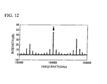
- FIG. 12 illustrates an emission spectrum at threshold of laser emission calculated by a computer simulation for threshold by using the wavelength changeable semiconductor laser having two SG-DR waveguides shown in FIG. 11 .
- the horizontal axis of FIG. 12 indicates frequency.
- the vertical axis of FIG. 12 indicates light intensity.
- lasers are emitted at 195600 GHz.
- the wavelength changeable range is, for example, approximately from 192000 GHz through to 196000 GHz.
- optical longitudinal mode intervals of the two SG-DR wavlengths are set respectively at 194 GHz and at 184 GHz and the difference between the intervals is 10 GHz.
- the difference between the optical longitudinal mode peak frequencies of the two SG-DR wavelengths is reduced at the optical longitudinal mode next to 194000 GHz. Accordingly, there is a problem that a laser tends to be emitted at the optical longitudinal mode next to the desirable frequency.
- a case where two SG-DR wavelengths are used is mentioned above.
- the same phenomenon occurs in a semiconductor laser in which a FP waveguide and a SG-DR waveguide are combined or a SG-DR waveguide and a SG-DFB waveguide are combined.
- a whole point of the mode degradation in a conventional art is that the semiconductor has a little wavelength dependence of an optical longitudinal mode peak reflectivity of a reflection spectrum. That is, it is very difficult to restrain the mode degradation of a laser emission of a wavelength changeable laser having a SG-DR waveguide of the conventional art and being capable of changing a wavelength in a broad range.
- the method of enhancing a reflectivity at a wavelength around a given wavelength by using a diffractive grating having various pitches is known, as mentioned in Document 11.
- the diffractive grating has no clear optical longitudinal modes like those of SG-DR waveguide. Therefore, there is a problem that it is difficult to restrain an emission of the FP waveguide, the SG-DR waveguide or the SG-DFB waveguide combined to the SG-DR wavelength at an optical longitudinal mode next to the desirable mode.
- US 6,782,164 B1 discloses a thermally wavelength tunable laser including a core, the core including more than one diffraction grating, and thermo-optical material adjacent to each diffraction grating.
- the chosen diffraction grating can be tuned over a selected wavelength range.
- different non-overlapping wavelength ranges can be selected and the laser can be tuned over a broad range of wavelengths.
- US 2003/0147588A1 discloses an optical waveguide device comprising a plurality of step-chirped, sampled fiber Bragg gratings which are chirped in a step-wise manner from one sampling segment to the next according to a chirp rate. Each sampling segment has a uniform grating period within the sampling segment.
- the step-chirped grating chirp rate may be selected to compensate for dispersion of signals over a transmission fiber connected to the optical waveguide device.
- WO 96/24079 discloses a light transmitting device comprising a broadband Bragg grating that is formed in the direction of light propagation with grating regions of alternatingly high and low refractive index.
- the grating regions are formed with periodicity P and are structured as to amplitude, periodicity and/or phase in a manner which varies periodically with a modulation period L>P.
- either one or the other or both of the grating period P and the modulation period L is or are chirped over substantially the full extent of the grating.
- the grating exhibits a spectral response in which broad reflection peaks appear at each side of a reflection peak centered on the Bragg wavelength and fall under an envelope determined by the Fourier transform of the periodic modulation function.
- US2004/0218639A1 discloses a tunable semiconductor laser in which a sampled grating distributed feedback (SG-DFB) structure portion and a sampled grating distributed Bragg reflector (SG-DBR) structure portion are integrated.
- the refractive index is varied in accordance with a current applied to the phase control area in the SG-DFB structure portion and the SG-DBR structure portion, whereby the wavelength can be continuously or discontinuously tuned.
- the present invention provides a semiconductor laser having a newly structured SG-DR waveguide and can stabilize the laser emission mode.
- a semiconductor laser comprising: a first reflector that has a plurality of segments, each segment of the first reflector having a first area including a diffractive grating and a second area that is a space area, optical lengths of at least two of the second areas of the segments being different from each other, and a refractive-index of each of the segments of the first reflector being changeable; a second reflector that has a plurality of segments, each segment of the second reflector having a first area including a diffractive grating and a second area that is a space area, optical lengths of the second areas of the segments of the second reflector being substantially equal to each other; and a plurality of heaters configured to control a refractive-index of each of the segments respectively of the first reflector; wherein the respective diffractive gratings of the first areas of the first reflector and the second reflector are equal in pitch to one another; and optical lengths of the second areas of the segments of the
- peak reflection intensity of the optical longitudinal mode of the first diffractive grating area has wavelength dependence, because the optical lengths of at least two of the second areas are different from each other.
- the peak reflectivity of the optical longitudinal mode of the first diffractive grating area indicates relatively high in a given wavelength range.
- a method of controlling a semiconductor laser comprising: a first reflector having a plurality of segments, each segment of the first reflector having a first area including a diffractive grating and a second area that is a space area, optical lengths of at least two of the second areas of the first reflector being different from each other, and the refractive-index of each of the segments being changeable; a second reflector having a plurality of segments, each segment of the second reflector having a first area including a diffractive grating and a second area that is a space area, optical lengths of the second areas of the segments of the second reflector being substantially equal to each other, the respective diffractive gratings of the first areas of the first reflector and the second reflector being equal in pitch to one another, and optical lengths of the second areas of the segments of the first reflector being larger than those of the second areas of the segments of the second reflector; and a plurality of heaters configured
- the refractive-indexes of at least two segments are controlled to be different from each other.
- the peak wavelengths of the optical longitudinal modes of the first diffractive grating area and the intensities of the optical longitudinal modes are controlled.
- FIG. 1 illustrates a block diagram of a laser device 100 in accordance with a first embodiment of the present invention.
- the laser device 100 has a laser portion 200 and a controller 300, as shown in FIG. 1 .
- the controller 300 has a central processing unit (CPU), a read only memory (ROM) and so on.
- the controller 300 stores a control information, a control program and so on of the laser portion 200.
- the controller 300 controls a laser emission wavelength of the laser portion 200 by controlling an electrical signal such as a current to be provided to the laser portion 200.
- FIG. 2A and FIG. 2B illustrate a detail of the laser portion 200.
- FIG. 2A illustrates a top view of the laser portion 200.
- FIG. 2B illustrates a cross sectional view taken along a line A-A of FIG. 2A .
- a description will be given, with reference to FIG. 2A and FIG. 2B , of the laser portion 200.
- the laser portion 200 has a structure in which a Chirped Sampled Grating Distributed Reflector (CSG-DR) area A, a Gain area B and a SG-DR area C are coupled in order.
- CSG-DR Chirped Sampled Grating Distributed Reflector
- the CSG-DR area A has a structure in which a waveguide core 3, a cladding layer 6 and an insulating layer 8 are laminated on a substrate 1 in order and thin film resistors 11, power electrodes 12 and a grand electrode 13 are laminated on the insulating layer 8.
- the gain area B has a structure in which a waveguide core 4, the cladding layer 6, a contact layer 7 and an electrode 14 are laminated on the substrate 1 in order.
- the SG-DR area C has a structure in which a waveguide core 5, the cladding layer 6 and the insulating layer 8 are laminated on the substrate 1 in order.
- the substrate 1 and the cladding layer 6 of the CSG-DR area A, the Gain area B and the SG-DR area C are formed as a unit respectively.
- the waveguides cores 3 through 5 are formed on a same plane and form a waveguide core together.
- a low reflecting coating 9 is formed on end faces of the substrate 1, the waveguide core 5 and the cladding layer 6 at the SG-DR area C side.
- a low reflecting coating 10 is formed on end faces of the substrate 1, the waveguide core 3 and the cladding layer 6 at the CSG-DR area A side.
- Sampled diffractive gratings 2 are formed at given intervals in the waveguide cores 3 and 5. The sampled grating is thus formed.
- the substrate 1 is, for example, a crystalline substrate composed of InP.
- the waveguide cores 3 and 5 are, for example, composed of InGaAsP crystalline having an absorption edge wavelength at shorter wavelengths side relative to the laser emission wavelength.
- PL wavelength of the waveguide cores 3 and 5 is approximately 1.3 ⁇ m.
- the waveguide core 4 is, for example, composed of InGaAsP crystalline amplifying a light of a desirable wavelength of a laser emission.
- the PL wavelength of the waveguide core 4 is approximately 1.57 ⁇ m.
- the coupling constant of the sampled diffractive grating 2 is approximately 200 cm -1 .
- the pitch of the sampled diffractive gratings is approximately 0.24 ⁇ m.
- the number of asperity of the sampled diffractive gratins 2 is approximately 17.
- the length of the sampled diffractive grating 2 is approximately 4 ⁇ m.
- the bragg wavelength of the sampled diffractive grating 2 is approximately 1.55 ⁇ m. In this case, the reflectivity against the bragg wavelength of the sampled diffractive grating 2 is approximately 1 %.
- the segment is an area in which one area having the sampled diffractive grating 2 and one space area not having the sampled diffractive grating 2 are combined in a waveguide core.
- the number of the segments is increased.
- a mode stability of a laser emission is thus improved.
- element length is increased if the number of the segments is increased.
- the mode stability is saturated because of an internal loss in the waveguide core 3, when total length of the waveguide core 3 is over 2 mm. It is, therefore, preferable that the number of the segments in the waveguide core 3 is approximately 5.
- optical longitudinal mode wavelength of a waveguide core it is possible to change an optical longitudinal mode wavelength of a waveguide core easily, when the length of each segment is increased and the optical longitudinal mode spacing is reduced. In this case, however, the length of the waveguide core is increased.
- lengths of the segments in the waveguide core 3 are, for example, 260 ⁇ m, 265 ⁇ m, 270 ⁇ m, 275 ⁇ m and 280 ⁇ m in order from the Gain area B side, in the embodiment.
- the optical longitudinal mode spacings of the segments in this case are 176 GHz, 173 GHz, 170 GHz, 167 GHz and 164 GHz.
- the length of each segment changes dependent on the length of the space area.
- the segments mentioned above are arranged in an opposite direction. It is not necessary that all of the lengths of the segments are different from each other. The length difference between the segments may differ.
- the configuration of the embodiment has an advantage in control viewpoint as mentioned later, because change amounts of refractive-index for wavelength control of the segments next to each other is constant in the embodiment.
- the number of the segments in the waveguide core 5 is preferably as same as that of the waveguide core 3, and is, for example, 5.
- Each length of the segments in the waveguide core 5 is substantially equal to each other, and is, for example, 240 ⁇ m. "Substantially equal" means that differences between each of the space areas are lower than 1 % of the average length of the space areas.
- a diffractive grating pattern is formed on whole area of a resist coated on the substrate 1 by the interference exposure method.
- a pattern of the space areas to divide the diffractive grating pattern on the substrate 1 are formed by the partial exposure method with an exposure mask having an opening and shielding a light partially.
- the structure of the sampled diffractive grating 2 is formed.
- the sampled diffractive grating 2 in accordance with the embodiment, in which phase relationships between each diffractive grating are determined, is formed when the resist pattern is printed on the substrate 1.
- the cladding layer 6 is composed of InP, constricts a current and confines a laser light traveling in the waveguide cores 3, 4 and 5.
- the contact layer 7 is composed of InGaAsP crystalline.
- the insulating layer 8 is a protection film composed of such as SiN or SiO 2 .
- the low reflecting coatings 9 and 10 are, for example, composed of a dielectric film including MgF 2 and TiON. The reflectivity of the low reflecting coatings 9 and 10 is, for example, lower than 0.3 %.
- the thin film resistors 11 are composed of such as NiCr, and control the temperature of the segments in the waveguide core 3 based on the current intensity provided from the controller 300 in FIG. 1 .
- Each of the thin film resistors 11 is formed on the insulating layer 8 above each of the segments in the waveguide core 3.
- Each of the power electrodes 12 is connected to each of the thin film resistors 11.
- the grand electrode 13 is connected to the thin film resistors 11.
- the power electrodes 12, the grand electrode 13 and the electrode 14 are composed of a conductive material such as Au.
- a given current is provided to the electrode 14 from the controller 300 in FIG. 1 .
- a light is generated in the waveguide core 4.
- the light propagates in the waveguide cores 3, 4 and 5, is reflected and amplified repeatedly, and is emitted toward outside.
- FIG. 3 illustrates a calculation example of reflection spectrums of the waveguide core 3 and reflection spectrums of the waveguide core 5.
- a horizontal axis of FIG. 3 indicates frequency.
- a vertical axis of FIG. 3 indicates reflectivity.
- the calculation example is simplified in FIG. 3 .
- the peak reflectivity of the waveguide core 3 indicates relatively high around 194000 GHz, and indicates a local maximum value at 194000 GHz. It is because the phase of the light traveling among the segments in the waveguide core is a value of integral multiplication of 2 n at 194000 GHz.
- the peak reflectivity of the waveguide core 3 is reduced when the frequency of the peak reflectivity is as far from 194000 GHz. It is because phase-matched superposition does not occur, as the optical longitudinal mode spacings of the segments are slightly different from each other. In the embodiment, a difference between the local maximum value of the peak reflectivity and the local minimum value of the peak reflectivity is approximately 5 dB. In addition, as shown in lower figure in FIG. 3 , the peak reflectivity indicates a constant value at any optical longitudinal modes.
- the optical longitudinal mode of the waveguide core 3 corresponds to the optical longitudinal mode of the waveguide core 5 at 195400 GHz and at 192600 GHz besides at 194000GHz.
- the reflectivity of the waveguide core 3 at 195400 GHz and at 192600 GHz is small enough relative to that at 194000 GHz.
- the occurrence possibility of laser emission at 195400 GHz and at 192600 GHz is, therefore, small.
- the peak reflection intensity of the optical longitudinal mode of the waveguide core 3 has wavelength dependence in the laser portion 200 in accordance with the embodiment. That is, the peak reflection intensity of the optical longitudinal mode of the wavegide core 3 changes based on the wavelength. On the contrary, the peak reflection intensity of the waveguide core 5 does not have wavelength dependence. It is possible to restrain a laser emission within a wavelength range in which the peak reflection intensity of the optical longitudinal mode of the waveguide core 3 is relatively low, and to obtain a stabilized laser emission within a wavelength range in which the peak reflection intensity of the optical longitudinal mode of the waveguide core 3 is relatively high.
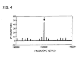
- FIG. 4 illustrates an emission spectrum at threshold of laser emission calculated by a computer simulation for threshold gain.
- the horizontal axis of FIG. 4 indicates frequency.
- the vertical axis of FIG. 4 indicates light intensity.
- the reflectivity at the end face is assumed 0 %.
- the optical longitudinal mode easy to be emitted next to the desirable optical longitudinal mode at 194000 GHz is the next optical longitudinal mode at lower frequency side.
- a difference between each of the threshold gains is 4 cm -1 . In this case, it is possible to obtain a stabilized laser emission. As mentioned above, the stabilized single mode laser emission is obtained, in the embodiment.
- the lengths of the segments increase by 5 ⁇ m from 260 ⁇ m to 280 ⁇ m.
- the result of the computer simulation for threshold gain shows that the mode stability is degraded particularly when the minimum difference between each of the lengths of the segments in the waveguide core 3 whose lengths are different from each other is out of the range 1 % to 6 % of the average length of the space areas.
- the minimum difference is lower than 1 % of the average length of the space areas, the reflection spectrum is closer to that of a conventional SG-DR waveguide. That is, the occurrence possibility of a laser emission at an optical longitudinal wavelength far from the desirable wavelength is high.
- the minimum difference is higher than 6 % of the average length of the space areas, another wavelength of the local maximum of the peak reflectivity is within the wavelength range in which the laser emission wavelength moves. That is, the occurrence possibility of the laser emission at frequencies of the desirable wavelength and another wavelength whose reflectivity is local maximum is high. Accordingly, the mode stability is degraded seriously. It is, therefore, preferable that the minimum difference between each of the lengths of the segments in the waveguide core 3 whose lengths are different from each other is within the range 1 % to 6 % of the average length of the space areas.
- the differences between each of the segments in the waveguide core 3 may be different from each other, although the differences are equal to each other in the embodiment.
- the control of the laser emission wavelength is complicated when the differences are not equal, because the change amount of refractive-index necessary for the wavelength change is complicated. Accordingly, it is advantageous in a control algorithm viewpoint that minimum values between the differences between each of the lengths of the segments and the minimum differences between each of the lengths of the segments other than those having a same length are equal. It is because the change amount of the refractive-index of the segments is integral multiplication of a given unit change amount, when the differences are equal.
- the waveguide core 3 has an equivalent refractive-index so that the peak reflectivity indicates local maximum at 194000 GHz when there is no temperature gradient.
- the equivalent of the waveguide core 3 is 3.2086 in this case.
- the equivalent refractive-index of the waveguide core 3 changes by approximately 0.0002 for every 1 degree C.
- FIG. 5 illustrates reflection spectrums of the waveguide core 3 in a case where the temperatures of the segments are controlled so as to be lower as the length of the segment is smaller and where the temperature difference between the segments next to each other in the waveguide core 3 is 2 degrees C.
- the horizontal axis of FIG. 5 indicates frequency.
- the vertical axis of FIG. 5 indicates reflectivity.
- the frequency of the local maximum peak reflectivity of the waveguide core 3 is 192500 GHz in a case where the difference between each of the temperatures of the segments in the waveguide core 3. It is possible to shift the frequency of the local maximum peak reflectivity by -1500 GHz, when the difference between each of the segments is set 2 degrees C. In contrast, it is possible to shift the frequency of the local maximum peak reflectivity by 1500 GHz, when the difference between each of the segments is set -2 degrees C. As mentioned above, it is possible to change the local maximum of the peak reflectivity by changing the differences between each of the segments. The light intensity of each optical longitudinal mode changes based on the temperature gradient but the frequencies of those do not change.
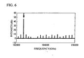
- FIG. 6 illustrates emission spectrums at threshold of laser emission calculated by a computer simulation for threshold gain in a case of FIG.5 .
- the horizontal axis of FIG. 6 indicates frequency.
- the vertical axis of FIG. 6 indicates light intensity.
- the reflectivity at the end face is assumed 0 %.
- the stabilized single mode laser emission is obtained at 192500 GHz, a frequency of the desirable laser emission.
- the laser portion 200 is operated with entire part thereof being arranged on a temperature control device.
- the average temperature of the waveguide core 3 changes when the temperature of the waveguide core 5 is changed by the temperature control device. This does not cause a problem, however. It is because that the changing of the wavelengths is possible when the difference between the temperature of the waveguide core 5 and the average temperature of the waveguide core 3 are controlled. In particular, the changing of the wavelengths is achieved easily when the length differences between each of the segments next to each other are equal and the segments are combined in descending order or in ascending order of length. In this case, it is possible to keep the stable laser emission because the temperature differences are difficult to be disturbed by the temperature change of outside.
- the optical length of each segment may be determined by another arrangement or method, although the optical length of each segment is determined based on the length of the space areas.
- the optical length of each segment may be determined based on materials of the space areas or the segments.
- the wavelengths of the optical longitudinal modes may be controlled as well as the maximum intensity of the optical longitudinal modes when required, although the laser emission wavelength is controlled by keeping the wavelengths of the optical longitudinal modes constant and changing the maximum intensity of the optical longitudinal modes.
- the temperature of each segment may be controlled so that the average temperature of the segments is different from that before the temperature control. It is possible to control the wavelengths of the optical longitudinal modes as well as the intensity of those when the average temperature of each segment is controlled to be a temperature at which the desirable optical longitudinal mode wavelengths are obtained, because the optical longitudinal modes are changeable in the condition.
- the sampled diffractive grating 2 corresponds to the diffractive grating.
- the area having the sampled diffractive grating in the waveguide core corresponds to the first area.
- the space area corresponds to the second area.
- the waveguide core 3 corresponds to the first reflector.
- the waveguide core 4 corresponds to the gain area.
- the waveguide core 5 corresponds to the second reflector.
- the thin film resistor 11 corresponds to the heater.
- the laser portion 200 corresponds to the semiconductor laser or the optical element.
- the laser device 100a has a laser portion 200a instead of the laser portion 200, being different from the laser device 100 shown in FIG. 1 .
- a description will be given of the laser portion 200a.
- FIG. 7 illustrates a schematic cross sectional view of the laser portion 200a.
- the laser portion 200a has a Phase Shift (PS) area D between the Gain area B and the SG-DR area C, being different from the laser portion 200.
- the PS area D has a structure in which a waveguide core 15, the cladding layer 6, the contact layer 7 and an electrode 16 are laminated on the substrate 1.
- the substrate 1 and the cladding layer 6 of the CSG-DR area A, the Gain area B, the PS area D and the SG-DR area C are formed as a unit respectively.
- the waveguide cores 3, 4, 5 and 15 are formed on a same plane and form one waveguide core together.
- the insulating layer 8 is also formed between the electrode 14 and the electrode 16.
- the waveguide core 15 is composed of InGaAsP crystalline having an absorption edge wavelength at shorter wavelengths side relative to the laser emission wavelength, as well as the waveguide core 3.
- the waveguide core 15 may be composed of the same material as the waveguide core 3 in the CSG-DR area A.
- the electrode 16 is an electrode to provide a current to the PS area D, and is composed of a conductive material such as Au.
- the PS area D adjusts a phase in the waveguide core 15 based on the current provided to the electrode 16 so that a phase of a light at the desirable wavelength reflected by the waveguide core 3 corresponds to that reflected by the waveguide core 5. It is, therefore, possible to obtain a stable laser emission at the desirable wavelength from the laser portion 200a.
- the PS area D corresponds to the phase adjusting area.
- the laser portion 200a corresponds to the semiconductor laser or the optical element.
- the laser device 100b has a laser portion 200b instead of the laser portion 200, being different from the laser device 100 shown in FIG. 1 .
- a description will be given of the laser portion 200b.
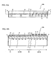
- FIG. 8A and FIG. 8B illustrate a detail of the laser portion 200b.
- FIG. 8A illustrates a top view of the laser portion 200b.
- FIG. 8B illustrates a cross sectional view taken along a line B-B of FIG. 8A .
- the laser portion 200b has the PS area D, a SG-DFB area E and a Power Control (PC) area F instead of the Gain area B and the SG-DR area C.
- PC Power Control
- the laser portion 200b has a structure in which the CSG-DR area A, the PS area D, the SG-DFB area E and the PC area F are coupled in order.
- the SG-DFB area E has a structure in which a waveguide core 17, the cladding layer 6, the contact layer 7 and an electrode 18 are laminated on the substrate 1 in order.
- the PC area F has a structure in which a waveguide core 19, the cladding layer 6, the contact layer 7 and an electrode 20 are laminated on the substrate 1 in order.
- the low reflecting coating 9 is formed on end faces of the substrate 1, the waveguide core 19 and the cladding layer 6 at the PC area F side.
- the substrate 1 and the cladding layer 6 of the CSG-DR area A, PS area D, the SG-DFB area E and the PC area F are formed as a unit respectively.
- the waveguide cores 3, 15, 17 and 19 are formed on a same plane and form one waveguide core together.
- the insulating layer 8 is also formed between the electrode 16 and the electrode 18 and between the electrode 18 and the electrode 20.
- the sampled diffractive gratings 2 are formed in the waveguide core 17 at a given interval. The sampled grating is thus formed.
- the waveguide core 17 is, for example, composed of InGaAsP crystalline amplifying an emitted laser of a desirable wavelength.
- the PL wavelength of the waveguide core 17 is approximately 1.57 ⁇ m.
- the number of the segments in the waveguide core 17 is preferably as same as that of the waveguide core 3, and is, for example, 5.
- Each length of the segments in the waveguide core 17 is substantially equal to each other, and is, for example, 240 ⁇ m.
- the waveguide core 19 is composed of InGaAsP crystalline to change an output of an outgoing light.
- the PL wavelength of the waveguide core 19 is approximately 1.57 ⁇ m.
- a given current is provided to the electrode 18 from the controller 300 in FIG. 1 .
- a light is generated in the waveguide core 17.
- the light is amplified in the waveguide core 19, propagates in the waveguide cores 3, 15, 17 and 19, is reflected and amplified repeatedly and is emitted toward outside.
- a given current is provided to the electrode 20 from the controller 300. And the output of the outgoing light is kept constant.
- the PL wavelengths of the waveguide cores 17 and 19 may be different from each other, although being equal to each other in the embodiment. However, it is possible to form the waveguide cores 17 and 19 in a same process, when the PL wavelengths of the waveguide cores 17 and 19 are equal to each other. In this case, the manufacturing cost is reduced. It is thus easy to manufacture the laser device 100b.
- the waveguide core 19 When an absorbing layer having an absorption edge wavelength at shorter wavelengths side relative to the laser emission wavelength is used as the waveguide core 19, it is possible to enhance the loss of laser light propagation by providing a current to the absorbing layer. It is, therefore, possible to control the intensity of the outgoing light emitted from an end face.
- a reflectivity toward a segment closest to the end face of the waveguide core 17 is under -30 dB by generating a propagation loss of -3 dB of one way in the absorbing layer, even if the reflectivity of the low reflecting coating 9 is approximately 0.3 %.
- the waveguide core 17 corresponds to the second reflector.
- the waveguide core 19 corresponds to the light absorption area or the light amplification area.
- the laser portion 200b corresponds to the semiconductor laser or the optical element.
- FIG. 9 illustrates an entire structure of the laser device 100c.
- the laser device 100c has a laser module 30 and a controller 40.
- the laser module 30 has an optical element 31, a light amplification portion 32, an optical element 33, a temperature control device 34 and a thermistor 35.
- the optical element 31, the light amplification portion 32 and the optical element 33 are arranged on the temperature control device so as to form an optical axis.
- the optical element 31 is an optical element having the CSG-DR area A mentioned above.
- the optical element 33 is an optical element having the SG-DR area C mentioned above.
- the light amplification portion 32 receives an instruction from the controller 40, amplifies an input light having a given effective wavelength range, and outputs a laser light.
- the laser light output from the amplification portion 32 propagates in the optical elements 31 and 33 and the light amplification portion 32, is reflected and amplified repeatedly and is emitted toward outside.
- the thermistor 35 detects the temperature of the temperature control device 34 and provides the detected result to the controller 40. In addition, a detection result of the optical output from outside is provided to the controller 40.
- the controller 40 controls the temperature of the temperature control device 34, the temperature of each segment of the CSG-DR area A in the optical element 31, and the light amplification portion 32, based on the detection result of the thermistor 35 and the detection result of the optical output from outside.
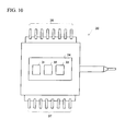
- FIG. 10 illustrates a detail view of the laser module 30.
- the laser module 30 has terminals 36 for inputting a signal from the controller 40 and terminals 37 for outputting a signal from the thermistor 35.
- the terminals 36 include a terminal for controlling the temperature control device 34, a terminal for controlling the temperature of each segment of the CSG-DR area A in the optical element 31, and a terminal controlling the light amplification portion 32.
- the positions of the terminals 36 and the terminals 37 are not limited. It is not necessary to arrange the terminals 36 at opposite side of the terminals 37.
- the terminals 36 and the terminals 37 may be arranged at a same side.
- the terminal 37 may be arranged between the terminals 36.
- a signal wiring for inputting from the controller or for outputting to the controller is downsized, when the optical elements are moduled. It is, therefore, possible to downsize the laser device.
- a laser module in which the laser portion 200 in accordance with the first embodiment is moduled and terminals to be connected to the power electrode 12 and the electrode 14 are provided, may be structured.
- a laser module in which the laser portion 200a in accordance with the second embodiment is moduled and terminals to be connected to the power electrode 12 and the electrodes 14 and 16 are provided, may be structure.
- a laser module, in which the laser portion 200b is moduled and terminals to be connected to the power electrode 12 and the electrodes 16, 18 and 20 are provided, may be structured.
Landscapes
- Physics & Mathematics (AREA)
- Condensed Matter Physics & Semiconductors (AREA)
- General Physics & Mathematics (AREA)
- Electromagnetism (AREA)
- Optics & Photonics (AREA)
- Semiconductor Lasers (AREA)
Description
- This invention generally relates to a semiconductor laser, an optical element, a laser device, and a method of controlling the semiconductor laser.
- Many organizations have developed a wavelength changeable semiconductor laser having an element which can emit various wavelengths laser lights, as Wavelength Division Multiplexing (WDM) communication using an optical fiber has been spread. The wavelength changeable semiconductor lasers proposed before now are classified broadly into a semiconductor laser having a Semiconductor Optical Amplifier (SOA) in an external resonator thereof and controlling an emitting wavelength with a wavelength selecting mechanism in the external resonator and a semiconductor laser having a structure in which a resonator acting as a wavelength selectable portion is built in a semiconductor element amplifying a laser light.
- A laser having a Sampled Grating Distributed Reflector (SG-DR) waveguide is disclosed as a typical wavelength changeable semiconductor laser, in which the resonator is built in the semiconductor element, in Japanese Patent Application Publication No.
9-270568 2004-336002 2003-17803 6,432,736 (hereinafter referred to as Document 4), United States Patent Application Publication No.2003/0128724 2002/0105991 (hereinafter referred to as Document 6), United States Patent Application Publication No.2002/0061047 (hereinafter referred to as Document 7), United States Patent No.6,590,924 (hereinafter referred to as Document 8), United States Patent No.6,317,539 (hereinafter referred to as Document 9), United States Patent No.4,896,325 (hereinafter referred to as Document 10), and Proc. IEEE, Selected Topics in Quantum Electronics, IEEE Journal of, Vol. 11, (hereinafter referred to as Document 11). The laser disclosed inDocument 8 uses a vernier effect. The laser has a structure in which SG-DR waveguides having different optical longitudinal mode interval from each other are respectively connected to both ends of a waveguide amplifying a laser light. The laser changes a reflection peak wavelength of optical longitudinal modes of one of the SG-DR wavelengths and a reflection peak wavelength of optical longitudinal modes of the other by changing temperature, current and so on, and emits a laser at a wavelength where the peak wavelengths corresponds to each other. - The laser disclosed in
Document 1 has a structure in which a SG-DR waveguide is combined to a Fabry-Perot (FP) resonator amplifying a laser light, changes reflection peak wavelengths of optical longitudinal mode of the FP resonator and the SG-DR waveguide by changing such as temperature or current, and emits a laser at a wavelength where the peak wavelengths correspond to each other. - Both of the lasers disclosed in
Document 1 andDocument 8 emit a laser based on a same principle using the vernier effect by the semiconductor waveguide. The laser disclosed inDocument 1 has an advantage relative to that disclosed inDocument 8, because an element length of the laser disclosed inDocument 1 is smaller than that of the laser disclosed inDocument 8. However, it is difficult that the laser inDocument 1 emits a stable laser, because the Q value of reflection spectrum of the simple FP resonator is small. And a structure, in which a SG-DR waveguide is combined to a Sampled Grating Distributed Feedback (SG-DFB) laser having a SG-DR waveguide core as a gain medium has been proposed inDocument 2. - The SG-DR waveguide has segments combined to each other, in which an area having a diffractive grating and an area not having a diffractive grating are combined to each other. The lengths of the segments in the conventional SG-DR wavelength are substantially equal to each other. When a wavelength is changed, the refraction index of each segment of the SG-DR waveguide is controlled in a same condition.
- However, a conventional wavelength changeable laser having a SG-DR waveguide tends to emit lasers besides a desirable laser, when the range where wavelength is changeable is spread. There is, therefore, a problem that the mode stability of the laser emission is degraded. A description will be given of the reason with reference to reflection spectrums of two SG-DR waveguides having different optical longitudinal mode interval from each other.
- It is necessary to match one of the optical longitudinal mode wavelengths of a SG-DR waveguide and one of the optical longitudinal mode wavelength of another SG-DR waveguide with a desirable wavelength or to match one of the optical longitudinal mode wavelengths of a SG-DR waveguide and one of the optical longitudinal mode wavelengths of a SG-DFB waveguide with the desirable wavelength. The optical longitudinal mode wavelengths of the SG-DR waveguide change when the refraction index of the SG-DR waveguide is changed. It is possible to change the refraction index by changing such as a current provided to the SG-DR waveguide or temperature of the SG-DR waveguide. For example, it is necessary to control the temperature of the SG-DR waveguide in a range of approximately 15 degrees C in order to match the optical longitudinal mode with a desirable wavelength with an element temperature, when the interval of the optical longitudinal modes of the SG-DR waveguide is approximately 200 GHz. A usual mechanism can achieve the temperature range.
-
FIG. 11 illustrates a calculation example of reflection spectrums of two SG-DR waveguides when the intervals of the optical longitudinal modes of the two SG-DR waveguides are respectively 194 GHz and 170 GHz. In this example, the temperatures of the two SG-DR waveguides are controlled so that the optical longitudinal modes of both SG-DR waveguides correspond at 194000 GHz. The horizontal axis ofFIG. 11 indicates frequency. The vertical axis ofFIG. 11 indicates a reflectivity of the SG-DR waveguides measured by dB. A laser emission is obtained at 194000 GHz, because both optical longitudinal modes of the SG-DR waveguides correspond to each other at 194000 GHz. However, the peak frequencies of both of the optical longitudinal modes discord to each other as the frequency gets away from 194000 GHz, because the intervals of the optical longitudinal modes are different from each other. No laser is emitted at other optical longitudinal mode frequencies around 194000 GHz. This is the vernier effect. - The peak reflections of the optical longitudinal modes of both of SG-DR waveguides correspond to each other approximately at 195400 GHz and 192600 GHz away from 194000 GHz by 1400 GHz. Lasers intend to be emitted at these two frequencies. Accordingly, the mode stability of a laser emission desired at 194000 GHz is degraded.
-
FIG. 12 illustrates an emission spectrum at threshold of laser emission calculated by a computer simulation for threshold by using the wavelength changeable semiconductor laser having two SG-DR waveguides shown inFIG. 11 . The horizontal axis ofFIG. 12 indicates frequency. The vertical axis ofFIG. 12 indicates light intensity. As shown inFIG. 12 , lasers are emitted at 195600 GHz. - It is necessary to reduce the difference between the optical longitudinal mode intervals of the two SG-DR waveguides so that the frequency where the reflection peaks correspond is out of the wavelength changeable range, and to structure a waveguide core having a gain getting smaller in a range out of the wavelength changeable range, in order to restrain the mode degradation caused by the mechanism. The wavelength changeable range is, for example, approximately from 192000 GHz through to 196000 GHz.
- Next, a description will be given of a calculation example in a case where optical longitudinal mode intervals of the two SG-DR wavlengths are set respectively at 194 GHz and at 184 GHz and the difference between the intervals is 10 GHz. In this case, there is no correspondence between the reflection peaks in the range from 192000 GHz through to 196000 GHz besides at 194000 GHz. However, the difference between the optical longitudinal mode peak frequencies of the two SG-DR wavelengths is reduced at the optical longitudinal mode next to 194000 GHz. Accordingly, there is a problem that a laser tends to be emitted at the optical longitudinal mode next to the desirable frequency.
- As mentioned above, there is a problem that an emission tends to occur at frequencies besides a desirable one and the mode stability of a laser emission is degraded in a conventional art, in a case where an element is structured so as to change a laser wavelength in a broad range.
- A case where two SG-DR wavelengths are used is mentioned above. The same phenomenon occurs in a semiconductor laser in which a FP waveguide and a SG-DR waveguide are combined or a SG-DR waveguide and a SG-DFB waveguide are combined. As shown in
FIG. 11 , a whole point of the mode degradation in a conventional art is that the semiconductor has a little wavelength dependence of an optical longitudinal mode peak reflectivity of a reflection spectrum. That is, it is very difficult to restrain the mode degradation of a laser emission of a wavelength changeable laser having a SG-DR waveguide of the conventional art and being capable of changing a wavelength in a broad range. - An art to solve the problem, in which pitches of sampled diffractive gratings change from one end to the other end, is disclosed in
Document 3. It is possible to enhance the reflectivity of an optical longitudinal mode around a given wavelength in the arrangement. However, it is necessary to use an advanced exposure technology using electron beam lithography in order to structure the diffractive gratings. In addition, it is very difficult to stabilize the phase relation between the sampled diffractive gratings of segments. There is a problem that interference effect of the reflected light from each segment is reduced. - The method of enhancing a reflectivity at a wavelength around a given wavelength by using a diffractive grating having various pitches is known, as mentioned in
Document 11. However, the diffractive grating has no clear optical longitudinal modes like those of SG-DR waveguide. Therefore, there is a problem that it is difficult to restrain an emission of the FP waveguide, the SG-DR waveguide or the SG-DFB waveguide combined to the SG-DR wavelength at an optical longitudinal mode next to the desirable mode. -
US 6,782,164 B1 discloses a thermally wavelength tunable laser including a core, the core including more than one diffraction grating, and thermo-optical material adjacent to each diffraction grating. By selectively changing the temperature and hence the refractive index in the thermo-optical material adjacent to a chosen diffraction grating, the chosen diffraction grating can be tuned over a selected wavelength range. By selecting different diffraction gratings, different non-overlapping wavelength ranges can be selected and the laser can be tuned over a broad range of wavelengths. -
US 2003/0147588A1 discloses an optical waveguide device comprising a plurality of step-chirped, sampled fiber Bragg gratings which are chirped in a step-wise manner from one sampling segment to the next according to a chirp rate. Each sampling segment has a uniform grating period within the sampling segment. The step-chirped grating chirp rate may be selected to compensate for dispersion of signals over a transmission fiber connected to the optical waveguide device. -
WO 96/24079 -
US2004/0218639A1 discloses a tunable semiconductor laser in which a sampled grating distributed feedback (SG-DFB) structure portion and a sampled grating distributed Bragg reflector (SG-DBR) structure portion are integrated. The refractive index is varied in accordance with a current applied to the phase control area in the SG-DFB structure portion and the SG-DBR structure portion, whereby the wavelength can be continuously or discontinuously tuned. - The present invention provides a semiconductor laser having a newly structured SG-DR waveguide and can stabilize the laser emission mode.
- According to a first aspect of the present invention, there is provided a semiconductor laser comprising: a first reflector that has a plurality of segments, each segment of the first reflector having a first area including a diffractive grating and a second area that is a space area, optical lengths of at least two of the second areas of the segments being different from each other, and a refractive-index of each of the segments of the first reflector being changeable; a second reflector that has a plurality of segments, each segment of the second reflector having a first area including a diffractive grating and a second area that is a space area, optical lengths of the second areas of the segments of the second reflector being substantially equal to each other; and a plurality of heaters configured to control a refractive-index of each of the segments respectively of the first reflector; wherein the respective diffractive gratings of the first areas of the first reflector and the second reflector are equal in pitch to one another; and optical lengths of the second areas of the segments of the first reflector are larger than those of the second areas of the segments of the second reflector.
- With the above-mentioned configuration, peak reflection intensity of the optical longitudinal mode of the first diffractive grating area has wavelength dependence, because the optical lengths of at least two of the second areas are different from each other. In this case, the peak reflectivity of the optical longitudinal mode of the first diffractive grating area indicates relatively high in a given wavelength range. And it is possible to restrain a laser emission in a wavelength range where the peak reflectivity of the optical longitudinal mode of the first diffractive grating area is relatively low. And it is possible to obtain a stabilized laser emission in the range where the peak reflectivity of the optical longitudinal mode of the first diffractive grating area indicates relatively high. In addition, it is possible to change the laser emission wavelength easily, because the refractive-index of each of the segments are changeable.
- According to a second aspect of the present invention, there is provided a method of controlling a semiconductor laser, the semiconductor laser comprising: a first reflector having a plurality of segments, each segment of the first reflector having a first area including a diffractive grating and a second area that is a space area, optical lengths of at least two of the second areas of the first reflector being different from each other, and the refractive-index of each of the segments being changeable; a second reflector having a plurality of segments, each segment of the second reflector having a first area including a diffractive grating and a second area that is a space area, optical lengths of the second areas of the segments of the second reflector being substantially equal to each other, the respective diffractive gratings of the first areas of the first reflector and the second reflector being equal in pitch to one another, and optical lengths of the second areas of the segments of the first reflector being larger than those of the second areas of the segments of the second reflector; and a plurality of heaters configured to control a refractive-index of each of the segments respectively of the first reflector; which method comprises a step of controlling peak wavelengths of optical longitudinal modes of the first reflector and intensities of the peak wavelengths by controlling refractive-indexes of at least two segments of the first reflector to be different from each other.
- With the above-mentioned configuration, the refractive-indexes of at least two segments are controlled to be different from each other. And the peak wavelengths of the optical longitudinal modes of the first diffractive grating area and the intensities of the optical longitudinal modes are controlled. In this case, it is possible to restrain a laser emission in a wavelength range where the peak reflectivity of the optical longitudinal mode of the first diffractive grating area is relatively low. And it is possible to obtain a stabilized laser emission in the range where the peak reflectivity of the optical longitudinal mode of the first diffractive grating area indicates relatively high. It is thus possible to stabilize the mode of the laser emission.
- Preferred embodiments of the present invention will be described in detail with reference to the following drawings, wherein:
-
FIG. 1 illustrates a block diagram of a laser device in accordance with a first embodiment of the present invention; -
FIG. 2A and FIG. 2B illustrate a detail of the laser portion; -
FIG. 3 illustrates a calculation example of reflection spectrums of the waveguide core; -
FIG. 4 illustrates an emission spectrum at threshold of laser emission calculated by a computer simulation for threshold gain; -
FIG. 5 illustrates reflection spectrums of the waveguide core in a case where the temperatures of the segments are controlled so as to be lower as the length of the segment is smaller and where the temperature difference between the segments next to each other in the waveguide core is 2 degrees C; -
FIG. 6 illustrates emission spectrums at threshold of laser emission calculated by a computer simulation for threshold gain in a case ofFIG.5 ; -
FIG. 7 illustrates a schematic cross sectional view of the laser portion in accordance with a second embodiment; -
FIG. 8A and FIG. 8B illustrate a detail of the laser portion in accordance with a third embodiment; -
FIG. 9 illustrates an entire structure of the laser device in accordance with a fourth embodiment; -
FIG. 10 illustrates a detail view of the laser module in accordance with the fourth embodiment; -
FIG. 11 illustrates a calculation example of reflection spectrums of two SG-DR waveguides when the intervals of the optical longitudinal modes of two SG-DR waveguides are respectively 194 GHz and 170 GHz; and -
FIG. 12 illustrates an emission spectrum at threshold of laser emission calculated by a computer simulation for threshold by using the wavelength changeable semiconductor laser having two SG-DR waveguides shown inFIG. 11 . - A description will now be given, with reference to the accompanying drawings, of embodiments of the present invention.
-
FIG. 1 illustrates a block diagram of alaser device 100 in accordance with a first embodiment of the present invention. Thelaser device 100 has alaser portion 200 and acontroller 300, as shown inFIG. 1 . Thecontroller 300 has a central processing unit (CPU), a read only memory (ROM) and so on. Thecontroller 300 stores a control information, a control program and so on of thelaser portion 200. Thecontroller 300 controls a laser emission wavelength of thelaser portion 200 by controlling an electrical signal such as a current to be provided to thelaser portion 200. -
FIG. 2A and FIG. 2B illustrate a detail of thelaser portion 200.FIG. 2A illustrates a top view of thelaser portion 200.FIG. 2B illustrates a cross sectional view taken along a line A-A ofFIG. 2A . A description will be given, with reference toFIG. 2A and FIG. 2B , of thelaser portion 200. As shown inFIG. 2A and FIG. 2B , thelaser portion 200 has a structure in which a Chirped Sampled Grating Distributed Reflector (CSG-DR) area A, a Gain area B and a SG-DR area C are coupled in order. - The CSG-DR area A has a structure in which a
waveguide core 3, acladding layer 6 and an insulatinglayer 8 are laminated on asubstrate 1 in order andthin film resistors 11,power electrodes 12 and agrand electrode 13 are laminated on the insulatinglayer 8. The gain area B has a structure in which awaveguide core 4, thecladding layer 6, acontact layer 7 and anelectrode 14 are laminated on thesubstrate 1 in order. The SG-DR area C has a structure in which awaveguide core 5, thecladding layer 6 and the insulatinglayer 8 are laminated on thesubstrate 1 in order. - The
substrate 1 and thecladding layer 6 of the CSG-DR area A, the Gain area B and the SG-DR area C are formed as a unit respectively. Thewaveguides cores 3 through 5 are formed on a same plane and form a waveguide core together. A low reflectingcoating 9 is formed on end faces of thesubstrate 1, thewaveguide core 5 and thecladding layer 6 at the SG-DR area C side. On the other hand, a low reflectingcoating 10 is formed on end faces of thesubstrate 1, thewaveguide core 3 and thecladding layer 6 at the CSG-DR area A side. Sampleddiffractive gratings 2 are formed at given intervals in thewaveguide cores - The
substrate 1 is, for example, a crystalline substrate composed of InP. Thewaveguide cores waveguide cores waveguide core 4 is, for example, composed of InGaAsP crystalline amplifying a light of a desirable wavelength of a laser emission. The PL wavelength of thewaveguide core 4 is approximately 1.57 µm. - The coupling constant of the sampled
diffractive grating 2 is approximately 200 cm-1. The pitch of the sampled diffractive gratings is approximately 0.24 µm. The number of asperity of the sampleddiffractive gratins 2 is approximately 17. The length of the sampleddiffractive grating 2 is approximately 4 µm. The bragg wavelength of the sampleddiffractive grating 2 is approximately 1.55 µm. In this case, the reflectivity against the bragg wavelength of the sampleddiffractive grating 2 is approximately 1 %. - Five segments are formed in the
waveguide core 3. Hereinafter, the segment is an area in which one area having the sampleddiffractive grating 2 and one space area not having the sampleddiffractive grating 2 are combined in a waveguide core. In general, it is possible to enhance an interference effect of light reflected by a sampled diffractive grating, when the number of the segments is increased. And a mode stability of a laser emission is thus improved. However, element length is increased if the number of the segments is increased. In addition, the mode stability is saturated because of an internal loss in thewaveguide core 3, when total length of thewaveguide core 3 is over 2 mm. It is, therefore, preferable that the number of the segments in thewaveguide core 3 is approximately 5. - It is possible to change an optical longitudinal mode wavelength of a waveguide core easily, when the length of each segment is increased and the optical longitudinal mode spacing is reduced. In this case, however, the length of the waveguide core is increased. On the contrary, lengths of the segments in the
waveguide core 3 are, for example, 260 µm, 265 µm, 270 µm, 275 µm and 280 µm in order from the Gain area B side, in the embodiment. The optical longitudinal mode spacings of the segments in this case are 176 GHz, 173 GHz, 170 GHz, 167 GHz and 164 GHz. - In the embodiment, the length of each segment changes dependent on the length of the space area. The segments mentioned above are arranged in an opposite direction. It is not necessary that all of the lengths of the segments are different from each other. The length difference between the segments may differ. However, the configuration of the embodiment has an advantage in control viewpoint as mentioned later, because change amounts of refractive-index for wavelength control of the segments next to each other is constant in the embodiment.
- The number of the segments in the
waveguide core 5 is preferably as same as that of thewaveguide core 3, and is, for example, 5. Each length of the segments in thewaveguide core 5 is substantially equal to each other, and is, for example, 240 µm. "Substantially equal" means that differences between each of the space areas are lower than 1 % of the average length of the space areas. - It is possible to form the SG-DR structure of the SG-DR area C by an art using a method such as an interference exposure method and a partial exposure method. At first, a diffractive grating pattern is formed on whole area of a resist coated on the
substrate 1 by the interference exposure method. Next, a pattern of the space areas to divide the diffractive grating pattern on thesubstrate 1 are formed by the partial exposure method with an exposure mask having an opening and shielding a light partially. When the resist is developed after the double exposure, the structure of the sampleddiffractive grating 2 is formed. The sampleddiffractive grating 2 in accordance with the embodiment, in which phase relationships between each diffractive grating are determined, is formed when the resist pattern is printed on thesubstrate 1. - It is possible to form the CSG-DR structure of the CSG-DR area A, when a pattern that can change the length of an area not having the sampled
diffractive grating 2 is used as an exposure mask for use of the partial exposure method mentioned above. In addition, it is possible to form the CSG-DR area A and the SG-DR area C in a same process if the exposure method is used. It is thus possible to shorten and simplify the manufacturing process. The manufacturing cost is, therefore, reduced. - The
cladding layer 6 is composed of InP, constricts a current and confines a laser light traveling in thewaveguide cores contact layer 7 is composed of InGaAsP crystalline. The insulatinglayer 8 is a protection film composed of such as SiN or SiO2. The low reflectingcoatings coatings - The
thin film resistors 11 are composed of such as NiCr, and control the temperature of the segments in thewaveguide core 3 based on the current intensity provided from thecontroller 300 inFIG. 1 . Each of thethin film resistors 11 is formed on the insulatinglayer 8 above each of the segments in thewaveguide core 3. Each of thepower electrodes 12 is connected to each of thethin film resistors 11. Thegrand electrode 13 is connected to thethin film resistors 11. Thepower electrodes 12, thegrand electrode 13 and theelectrode 14 are composed of a conductive material such as Au. - Next, a description will be given of an operation of the
laser portion 200. At first, a given current is provided to theelectrode 14 from thecontroller 300 inFIG. 1 . And a light is generated in thewaveguide core 4. The light propagates in thewaveguide cores -
FIG. 3 illustrates a calculation example of reflection spectrums of thewaveguide core 3 and reflection spectrums of thewaveguide core 5. A horizontal axis ofFIG. 3 indicates frequency. A vertical axis ofFIG. 3 indicates reflectivity. The calculation example is simplified inFIG. 3 . As shown in the upper figure inFIG. 3 , the peak reflectivity of thewaveguide core 3 indicates relatively high around 194000 GHz, and indicates a local maximum value at 194000 GHz. It is because the phase of the light traveling among the segments in the waveguide core is a value of integral multiplication of 2 n at 194000 GHz. - On the other hand, the peak reflectivity of the
waveguide core 3 is reduced when the frequency of the peak reflectivity is as far from 194000 GHz. It is because phase-matched superposition does not occur, as the optical longitudinal mode spacings of the segments are slightly different from each other. In the embodiment, a difference between the local maximum value of the peak reflectivity and the local minimum value of the peak reflectivity is approximately 5 dB. In addition, as shown in lower figure inFIG. 3 , the peak reflectivity indicates a constant value at any optical longitudinal modes. - The optical longitudinal mode of the
waveguide core 3 corresponds to the optical longitudinal mode of thewaveguide core 5 at 195400 GHz and at 192600 GHz besides at 194000GHz. However, the reflectivity of thewaveguide core 3 at 195400 GHz and at 192600 GHz is small enough relative to that at 194000 GHz. The occurrence possibility of laser emission at 195400 GHz and at 192600 GHz is, therefore, small. - The peak reflection intensity of the optical longitudinal mode of the
waveguide core 3 has wavelength dependence in thelaser portion 200 in accordance with the embodiment. That is, the peak reflection intensity of the optical longitudinal mode of thewavegide core 3 changes based on the wavelength. On the contrary, the peak reflection intensity of thewaveguide core 5 does not have wavelength dependence. It is possible to restrain a laser emission within a wavelength range in which the peak reflection intensity of the optical longitudinal mode of thewaveguide core 3 is relatively low, and to obtain a stabilized laser emission within a wavelength range in which the peak reflection intensity of the optical longitudinal mode of thewaveguide core 3 is relatively high. In addition, it is possible to control the laser emission wavelength easily, when the wavelength range in which the peak reflection intensity of the optical longitudinal mode is relatively high is changed with the change of the refractive-index of thewaveguide core 3. There is no affection to the waveguide light, although there are provided diffractive gratings at both end faces of thewaveguide cores -
FIG. 4 illustrates an emission spectrum at threshold of laser emission calculated by a computer simulation for threshold gain. The horizontal axis ofFIG. 4 indicates frequency. The vertical axis ofFIG. 4 indicates light intensity. In the analysis, the reflectivity at the end face is assumed 0 %. In the calculation example, the optical longitudinal mode easy to be emitted next to the desirable optical longitudinal mode at 194000 GHz is the next optical longitudinal mode at lower frequency side. However, a difference between each of the threshold gains is 4 cm-1 . In this case, it is possible to obtain a stabilized laser emission. As mentioned above, the stabilized single mode laser emission is obtained, in the embodiment. - In the embodiment, the lengths of the segments increase by 5 µm from 260 µm to 280 µm. The result of the computer simulation for threshold gain shows that the mode stability is degraded particularly when the minimum difference between each of the lengths of the segments in the
waveguide core 3 whose lengths are different from each other is out of therange 1 % to 6 % of the average length of the space areas. - A description will be qualitatively given of the mechanism of the degradation of the mode stability. When the minimum difference is lower than 1 % of the average length of the space areas, the reflection spectrum is closer to that of a conventional SG-DR waveguide. That is, the occurrence possibility of a laser emission at an optical longitudinal wavelength far from the desirable wavelength is high. In contrast, when the minimum difference is higher than 6 % of the average length of the space areas, another wavelength of the local maximum of the peak reflectivity is within the wavelength range in which the laser emission wavelength moves. That is, the occurrence possibility of the laser emission at frequencies of the desirable wavelength and another wavelength whose reflectivity is local maximum is high. Accordingly, the mode stability is degraded seriously. It is, therefore, preferable that the minimum difference between each of the lengths of the segments in the
waveguide core 3 whose lengths are different from each other is within therange 1 % to 6 % of the average length of the space areas. - The differences between each of the segments in the
waveguide core 3 may be different from each other, although the differences are equal to each other in the embodiment. The control of the laser emission wavelength is complicated when the differences are not equal, because the change amount of refractive-index necessary for the wavelength change is complicated. Accordingly, it is advantageous in a control algorithm viewpoint that minimum values between the differences between each of the lengths of the segments and the minimum differences between each of the lengths of the segments other than those having a same length are equal. It is because the change amount of the refractive-index of the segments is integral multiplication of a given unit change amount, when the differences are equal. - In addition, it is advantageous in the same viewpoint that differences between the lengths of the segments next to each other are equal and the segments are combined in descending order or in ascending order of length. It is because that it is possible to change the wavelength of the local maximum peak reflectivity when refractive-indexes of the segments are changed at a fixed gradient.
- It is possible to control the local maximum peak reflectivity of the
waveguide core 3 mentioned above by controlling the refractive-index of the segments in thewaveguide core 3 from outside. A description will be given of a controlling method of the local maximum peak reflectivity of thewaveguide core 3. At first, a given current is provided to each of thethin film resistors 11 through each of thepower electrodes 12 from thecontroller 300. The temperature of each segment in thewaveguide core 3 changes to a given value. The refractive-index of thewaveguide core 3 changes to a given value. The current passing through thethin film resistors 11 is recovered through thegrand electrode 13. - In the embodiment, the
waveguide core 3 has an equivalent refractive-index so that the peak reflectivity indicates local maximum at 194000 GHz when there is no temperature gradient. The equivalent of thewaveguide core 3 is 3.2086 in this case. In addition, the equivalent refractive-index of thewaveguide core 3 changes by approximately 0.0002 for every 1 degree C. -
FIG. 5 illustrates reflection spectrums of thewaveguide core 3 in a case where the temperatures of the segments are controlled so as to be lower as the length of the segment is smaller and where the temperature difference between the segments next to each other in thewaveguide core 3 is 2 degrees C. The horizontal axis ofFIG. 5 indicates frequency. The vertical axis ofFIG. 5 indicates reflectivity. - As shown in
FIG. 5 , the frequency of the local maximum peak reflectivity of thewaveguide core 3 is 192500 GHz in a case where the difference between each of the temperatures of the segments in thewaveguide core 3. It is possible to shift the frequency of the local maximum peak reflectivity by -1500 GHz, when the difference between each of the segments is set 2 degrees C. In contrast, it is possible to shift the frequency of the local maximum peak reflectivity by 1500 GHz, when the difference between each of the segments is set -2 degrees C. As mentioned above, it is possible to change the local maximum of the peak reflectivity by changing the differences between each of the segments. The light intensity of each optical longitudinal mode changes based on the temperature gradient but the frequencies of those do not change. -
FIG. 6 illustrates emission spectrums at threshold of laser emission calculated by a computer simulation for threshold gain in a case ofFIG.5 . The horizontal axis ofFIG. 6 indicates frequency. The vertical axis ofFIG. 6 indicates light intensity. In the analysis, the reflectivity at the end face is assumed 0 %. As shown inFIG. 6 , the stabilized single mode laser emission is obtained at 192500 GHz, a frequency of the desirable laser emission. - It is necessary to adjust the frequencies of the optical longitudinal modes by controlling the temperature of the
waveguide core 5 and the average temperature of thewaveguide core 3 as well as the temperature gradient in order to set the local maximum frequency of the reflection peak of the optical longitudinal mode to a desirable value. It is, therefore, necessary to control the wavelengths by controlling the temperature of thewaveguide core 5 and the average temperature and the temperature gradient of thewaveguide core 3, when the differences between the segments next to each other are equal and the segments are combined in descending order or in ascending order of length. However, a constant feedback control during the laser emission is not necessary, because the temperature gradient of thewaveguide core 3 does not change the frequency of the optical longitudinal mode. In addition, parameters to be controlled during the constant feedback control are only the temperature of thewaveguide core 5 and the average temperature of thewaveguide core 3 at a maximum. The arrangement in accordance with the embodiment is, therefore, advantageous in the control algorithm viewpoint. - It is usual that the
laser portion 200 is operated with entire part thereof being arranged on a temperature control device. The average temperature of thewaveguide core 3 changes when the temperature of thewaveguide core 5 is changed by the temperature control device. This does not cause a problem, however. It is because that the changing of the wavelengths is possible when the difference between the temperature of thewaveguide core 5 and the average temperature of thewaveguide core 3 are controlled. In particular, the changing of the wavelengths is achieved easily when the length differences between each of the segments next to each other are equal and the segments are combined in descending order or in ascending order of length. In this case, it is possible to keep the stable laser emission because the temperature differences are difficult to be disturbed by the temperature change of outside. - It is possible to control the refractive-index of each segment in the
waveguide core 3 by providing a current to each segment, although the refractive-index of each segment is controlled by the temperature control in the embodiment. In this case, it is possible to achieve the refractive-index control by arranging electrodes instead of thethin film resistors 11. The temperature control in accordance with the embodiment is more effective, because a loss of light propagation is generated in thewaveguide core 3 when a current is provided to thewaveguide core 3. - The optical length of each segment may be determined by another arrangement or method, although the optical length of each segment is determined based on the length of the space areas. For example, the optical length of each segment may be determined based on materials of the space areas or the segments. In addition, it is possible to control the refractive-index of each segment based on the change amount of temperature of each segment (temperature gradient) and the absolute value of temperature of each segment (average temperature), because it is possible to control the refractive-index of each segment based on the temperature of that.
- The wavelengths of the optical longitudinal modes may be controlled as well as the maximum intensity of the optical longitudinal modes when required, although the laser emission wavelength is controlled by keeping the wavelengths of the optical longitudinal modes constant and changing the maximum intensity of the optical longitudinal modes. In this case, the temperature of each segment may be controlled so that the average temperature of the segments is different from that before the temperature control. It is possible to control the wavelengths of the optical longitudinal modes as well as the intensity of those when the average temperature of each segment is controlled to be a temperature at which the desirable optical longitudinal mode wavelengths are obtained, because the optical longitudinal modes are changeable in the condition.
- In the embodiments, the sampled
diffractive grating 2 corresponds to the diffractive grating. The area having the sampled diffractive grating in the waveguide core corresponds to the first area. The space area corresponds to the second area. Thewaveguide core 3 corresponds to the first reflector. Thewaveguide core 4 corresponds to the gain area. Thewaveguide core 5 corresponds to the second reflector. Thethin film resistor 11 corresponds to the heater. Thelaser portion 200 corresponds to the semiconductor laser or the optical element. - Next, a description will be given of a laser device 100a in accordance with a second embodiment of the invention. The laser device 100a has a
laser portion 200a instead of thelaser portion 200, being different from thelaser device 100 shown inFIG. 1 . A description will be given of thelaser portion 200a. -
FIG. 7 illustrates a schematic cross sectional view of thelaser portion 200a. Thelaser portion 200a has a Phase Shift (PS) area D between the Gain area B and the SG-DR area C, being different from thelaser portion 200. The PS area D has a structure in which awaveguide core 15, thecladding layer 6, thecontact layer 7 and anelectrode 16 are laminated on thesubstrate 1. - The
substrate 1 and thecladding layer 6 of the CSG-DR area A, the Gain area B, the PS area D and the SG-DR area C are formed as a unit respectively. Thewaveguide cores layer 8 is also formed between theelectrode 14 and theelectrode 16. Thewaveguide core 15 is composed of InGaAsP crystalline having an absorption edge wavelength at shorter wavelengths side relative to the laser emission wavelength, as well as thewaveguide core 3. Thewaveguide core 15 may be composed of the same material as thewaveguide core 3 in the CSG-DR area A. Theelectrode 16 is an electrode to provide a current to the PS area D, and is composed of a conductive material such as Au. - The PS area D adjusts a phase in the
waveguide core 15 based on the current provided to theelectrode 16 so that a phase of a light at the desirable wavelength reflected by thewaveguide core 3 corresponds to that reflected by thewaveguide core 5. It is, therefore, possible to obtain a stable laser emission at the desirable wavelength from thelaser portion 200a. In the embodiment, the PS area D corresponds to the phase adjusting area. Thelaser portion 200a corresponds to the semiconductor laser or the optical element. - Next, a description will be given of a laser device 100b in accordance with a third embodiment. The laser device 100b has a
laser portion 200b instead of thelaser portion 200, being different from thelaser device 100 shown inFIG. 1 . A description will be given of thelaser portion 200b. -
FIG. 8A and FIG. 8B illustrate a detail of thelaser portion 200b.FIG. 8A illustrates a top view of thelaser portion 200b.FIG. 8B illustrates a cross sectional view taken along a line B-B ofFIG. 8A . A description will be given, with reference toFIG. 8A and FIG. 8B , of thelaser portion 200b. Thelaser portion 200b has the PS area D, a SG-DFB area E and a Power Control (PC) area F instead of the Gain area B and the SG-DR area C. - The
laser portion 200b has a structure in which the CSG-DR area A, the PS area D, the SG-DFB area E and the PC area F are coupled in order. The SG-DFB area E has a structure in which awaveguide core 17, thecladding layer 6, thecontact layer 7 and anelectrode 18 are laminated on thesubstrate 1 in order. The PC area F has a structure in which awaveguide core 19, thecladding layer 6, thecontact layer 7 and anelectrode 20 are laminated on thesubstrate 1 in order. The low reflectingcoating 9 is formed on end faces of thesubstrate 1, thewaveguide core 19 and thecladding layer 6 at the PC area F side. - The
substrate 1 and thecladding layer 6 of the CSG-DR area A, PS area D, the SG-DFB area E and the PC area F are formed as a unit respectively. Thewaveguide cores layer 8 is also formed between theelectrode 16 and theelectrode 18 and between theelectrode 18 and theelectrode 20. The sampleddiffractive gratings 2 are formed in thewaveguide core 17 at a given interval. The sampled grating is thus formed. - The
waveguide core 17 is, for example, composed of InGaAsP crystalline amplifying an emitted laser of a desirable wavelength. The PL wavelength of thewaveguide core 17 is approximately 1.57 µm. The number of the segments in thewaveguide core 17 is preferably as same as that of thewaveguide core 3, and is, for example, 5. Each length of the segments in thewaveguide core 17 is substantially equal to each other, and is, for example, 240 µm. Thewaveguide core 19 is composed of InGaAsP crystalline to change an output of an outgoing light. The PL wavelength of thewaveguide core 19 is approximately 1.57 µm. - Next, a description will be given of operation of the
laser portion 200b. At first, a given current is provided to theelectrode 18 from thecontroller 300 inFIG. 1 . And a light is generated in thewaveguide core 17. The light is amplified in thewaveguide core 19, propagates in thewaveguide cores electrode 20 from thecontroller 300. And the output of the outgoing light is kept constant. - The PL wavelengths of the
waveguide cores waveguide cores waveguide cores - When an absorbing layer having an absorption edge wavelength at shorter wavelengths side relative to the laser emission wavelength is used as the
waveguide core 19, it is possible to enhance the loss of laser light propagation by providing a current to the absorbing layer. It is, therefore, possible to control the intensity of the outgoing light emitted from an end face. In this case, a reflectivity toward a segment closest to the end face of thewaveguide core 17 is under -30 dB by generating a propagation loss of -3 dB of one way in the absorbing layer, even if the reflectivity of the low reflectingcoating 9 is approximately 0.3 %. And it is possible to stabilize the mode of the laser emission. This effect is obtained when thewaveguide core 17 is arranged to be inclined to the crystal axis. It is not necessary to change the current supply to thewaveguide core 17, when the control of the intensity of the outgoing light is used. It is, therefore, possible to restrain the change of the refraction-index of thewaveguide core 17. And it is possible to restrain the stability degradation of the laser emission being dependent on the refraction-index change of thewaveguide core 17. - In the embodiment, the
waveguide core 17 corresponds to the second reflector. Thewaveguide core 19 corresponds to the light absorption area or the light amplification area. Thelaser portion 200b corresponds to the semiconductor laser or the optical element. - Next, a description will be given of a
laser device 100c in accordance with a fourth embodiment.FIG. 9 illustrates an entire structure of thelaser device 100c. As shown inFIG. 9 , thelaser device 100c has alaser module 30 and acontroller 40. Thelaser module 30 has anoptical element 31, alight amplification portion 32, anoptical element 33, atemperature control device 34 and athermistor 35. Theoptical element 31, thelight amplification portion 32 and theoptical element 33 are arranged on the temperature control device so as to form an optical axis. - The
optical element 31 is an optical element having the CSG-DR area A mentioned above. Theoptical element 33 is an optical element having the SG-DR area C mentioned above. Thelight amplification portion 32 receives an instruction from thecontroller 40, amplifies an input light having a given effective wavelength range, and outputs a laser light. The laser light output from theamplification portion 32 propagates in theoptical elements light amplification portion 32, is reflected and amplified repeatedly and is emitted toward outside. Thethermistor 35 detects the temperature of thetemperature control device 34 and provides the detected result to thecontroller 40. In addition, a detection result of the optical output from outside is provided to thecontroller 40. Thecontroller 40 controls the temperature of thetemperature control device 34, the temperature of each segment of the CSG-DR area A in theoptical element 31, and thelight amplification portion 32, based on the detection result of thethermistor 35 and the detection result of the optical output from outside. -
FIG. 10 illustrates a detail view of thelaser module 30. As shown inFIG. 10 , thelaser module 30 hasterminals 36 for inputting a signal from thecontroller 40 andterminals 37 for outputting a signal from thethermistor 35. Theterminals 36 include a terminal for controlling thetemperature control device 34, a terminal for controlling the temperature of each segment of the CSG-DR area A in theoptical element 31, and a terminal controlling thelight amplification portion 32. The positions of theterminals 36 and theterminals 37 are not limited. It is not necessary to arrange theterminals 36 at opposite side of theterminals 37. Theterminals 36 and theterminals 37 may be arranged at a same side. The terminal 37 may be arranged between theterminals 36. - A signal wiring for inputting from the controller or for outputting to the controller is downsized, when the optical elements are moduled. It is, therefore, possible to downsize the laser device. In addition, a laser module, in which the
laser portion 200 in accordance with the first embodiment is moduled and terminals to be connected to thepower electrode 12 and theelectrode 14 are provided, may be structured. A laser module, in which thelaser portion 200a in accordance with the second embodiment is moduled and terminals to be connected to thepower electrode 12 and theelectrodes laser portion 200b is moduled and terminals to be connected to thepower electrode 12 and theelectrodes
Claims (13)
- A semiconductor laser (200, 200a, 200b) comprising:a first reflector (3) that has a plurality of segments,each segment of the first reflector (3) having a first area including a diffractive grating (2) and a second area that is a space area,optical lengths of at least two of the second areas of the segments being different from each other, anda refractive-index of each of the segments of the first reflector (3) being changeable;a second reflector (5; 17) that has a plurality of segments,each segment of the second reflector (5; 17) having a first area including a diffractive grating (2) and a second area that is a space area, optical lengths of the second areas of the segments of the second reflector (5; 17) being substantially equal to each other; anda plurality of heaters (11) configured to control a refractive-index of each of the segments respectively of the first reflector (3);wherein the respective diffractive gratings (2) of the first areas of the first reflector (3) and the second reflector (5; 17) are equal in pitch to one another; andoptical lengths of the second areas of the segments of the first reflector (3) are larger than those of the second areas of the segments of the second reflector (5; 17).
- The semiconductor laser as claimed in claim 1, wherein a minimum difference between the optical lengths of the second areas of the segments of the first reflector (3) is within 1 to 6 % of an average optical length of the second areas in the first reflector (3).
- The semiconductor laser as claimed in claim 1, wherein in the first reflector, in each case where the optical length of one of the second areas differs from at least two other ones of the second areas, the minimum value of the difference in the optical length between such second areas is equal to the minimum value of the difference between the differences in optical length between those second areas.
- The semiconductor laser as claimed in claim 1, wherein the segments of the first reflector (3) are arranged in an ascending order or a descending order of optical length.
- The semiconductor laser as claimed in claim 1, wherein a light absorption area (19) or a light amplification area (19) is provided at an end face of the semiconductor laser.
- The semiconductor laser as claimed in claim 1 further comprising a phase control area (D) for controlling a phase of a light in the first reflector (3) and the second reflector (5; 17).
- A semiconductor laser as claimed in claim 1, further comprising an optical amplifier (32), wherein the first reflector (3) forms a first optical element (31).
- The semiconductor laser as claimed in claim 7, wherein the first optical element (31) and the optical amplifier (32) are arranged on a temperature control device (34).
- A method of controlling a semiconductor laser,
the semiconductor laser comprising:a first reflector (3) having a plurality of segments,each segment of the first reflector (3) having a first area including a diffractive grating (2) and a second area that is a space area,optical lengths of at least two of the second areas of the first reflector (3) being different from each other, andthe refractive-index of each of the segments being changeable;a second reflector (5) having a plurality of segments, each segment of the second reflector (5; 17) having a first area including a diffractive grating (2) and a second area that is a space area, optical lengths of the second areas of the segments of the second reflector (5; 17) being substantially equal to each other, the respective diffractive gratings (2) of the first areas of the first reflector (3) and the second reflector (5; 17) being equal in pitch to one another, and optical lengths of the second areas of the segments of the first reflector (3) being larger than those of the second areas of the segments of the second reflector (5; 17); anda plurality of heaters (11) configured to control a refractive-index of each of the segments respectively of the first reflector (3);which method comprises a step of controlling peak wavelengths of optical longitudinal modes of the first reflector (3) and intensities of the peak wavelengths by controlling refractive-indexes of at least two segments of the first reflector to be different from each other. - The method as claimed in claim 9, wherein the controlling step is a step of controlling an average of the refractive-indexes of the segments to be constant so that the wavelengths of the optical longitudinal modes of the first reflector (3) are fixed and the intensities of the peak wavelengths are changed.
- The method as claimed in claim 9, wherein the controlling step is a step of controlling each of refractive-index differentials between the segments to be constant so that the wavelengths of the optical longitudinal modes of the first reflector (3) are changed and the intensities of the peak wavelengths are fixed.
- The method as claimed in claim 9, wherein the controlling step is a step of controlling the refractive-index of each segment so that the refractive-index of one of the segments is different from the refractive-index of the other segment.
- The method as claimed in claim 9, wherein the controlling step is a step of controlling the refractive-index of each segment by controlling a temperature of the segments.
Priority Applications (1)
| Application Number | Priority Date | Filing Date | Title |
|---|---|---|---|
| EP10171188A EP2244342A3 (en) | 2005-08-11 | 2006-08-08 | Semiconductor laser |
Applications Claiming Priority (1)
| Application Number | Priority Date | Filing Date | Title |
|---|---|---|---|
| JP2005232697A JP4657853B2 (en) | 2005-08-11 | 2005-08-11 | Semiconductor laser, laser module, optical component, laser device, semiconductor laser manufacturing method, and semiconductor laser control method |
Related Child Applications (1)
| Application Number | Title | Priority Date | Filing Date |
|---|---|---|---|
| EP10171188.5 Division-Into | 2010-07-29 |
Publications (3)
| Publication Number | Publication Date |
|---|---|
| EP1753104A2 EP1753104A2 (en) | 2007-02-14 |
| EP1753104A3 EP1753104A3 (en) | 2007-06-13 |
| EP1753104B1 true EP1753104B1 (en) | 2012-11-21 |
Family
ID=37467515
Family Applications (2)
| Application Number | Title | Priority Date | Filing Date |
|---|---|---|---|
| EP06254145A Active EP1753104B1 (en) | 2005-08-11 | 2006-08-08 | Semiconductor laser |
| EP10171188A Withdrawn EP2244342A3 (en) | 2005-08-11 | 2006-08-08 | Semiconductor laser |
Family Applications After (1)
| Application Number | Title | Priority Date | Filing Date |
|---|---|---|---|
| EP10171188A Withdrawn EP2244342A3 (en) | 2005-08-11 | 2006-08-08 | Semiconductor laser |
Country Status (4)
| Country | Link |
|---|---|
| US (2) | US8588266B2 (en) |
| EP (2) | EP1753104B1 (en) |
| JP (1) | JP4657853B2 (en) |
| CN (1) | CN1913261B (en) |
Families Citing this family (30)
| Publication number | Priority date | Publication date | Assignee | Title |
|---|---|---|---|---|
| US7894693B2 (en) | 2007-04-05 | 2011-02-22 | Eudyna Devices Inc. | Optical semiconductor device and method of controlling the same |
| JP5303124B2 (en) * | 2007-07-19 | 2013-10-02 | 住友電工デバイス・イノベーション株式会社 | Method for controlling semiconductor laser device |
| JP2009044141A (en) * | 2007-07-19 | 2009-02-26 | Eudyna Devices Inc | Optical device, and control method thereof |
| US7812594B2 (en) * | 2007-07-19 | 2010-10-12 | Eudyna Devices Inc. | Optical device and method of controlling the same |
| JP4943255B2 (en) * | 2007-07-20 | 2012-05-30 | 住友電工デバイス・イノベーション株式会社 | Semiconductor laser control method |
| JP5154581B2 (en) * | 2008-02-05 | 2013-02-27 | 住友電工デバイス・イノベーション株式会社 | Laser device and control data of laser device |
| JP2010153826A (en) * | 2008-11-25 | 2010-07-08 | Opnext Japan Inc | Wavelength-tunable filter and wavelength-tunable laser module |
| JP5474338B2 (en) | 2008-11-28 | 2014-04-16 | 住友電工デバイス・イノベーション株式会社 | Tuning method of semiconductor laser |
| JP5556137B2 (en) * | 2009-11-18 | 2014-07-23 | 住友電気工業株式会社 | Semiconductor laser device |
| JP5457873B2 (en) | 2010-02-18 | 2014-04-02 | 住友電工デバイス・イノベーション株式会社 | Control method of wavelength tunable laser |
| JP5499903B2 (en) * | 2010-05-27 | 2014-05-21 | 住友電気工業株式会社 | Semiconductor laser |
| JP5597029B2 (en) * | 2010-05-27 | 2014-10-01 | 住友電気工業株式会社 | Tunable semiconductor laser |
| JP2013033892A (en) | 2011-06-29 | 2013-02-14 | Sumitomo Electric Ind Ltd | Semiconductor laser and laser apparatus |
| JP6186864B2 (en) * | 2012-05-18 | 2017-08-30 | 住友電気工業株式会社 | Semiconductor laser |
| US8861556B2 (en) * | 2012-07-05 | 2014-10-14 | Jds Uniphase Corporation | Tunable Bragg grating and a tunable laser diode using same |
| US9791622B2 (en) * | 2013-09-12 | 2017-10-17 | Oclaro Japan, Inc. | Optical semiconductor resonator, optical semiconductor device, and optical module |
| JP6270387B2 (en) * | 2013-09-12 | 2018-01-31 | 日本オクラロ株式会社 | Semiconductor optical resonator, semiconductor optical device, and optical communication module |
| WO2015039273A1 (en) * | 2013-09-17 | 2015-03-26 | 华为技术有限公司 | Laser device, optical signal modulation method and optical network system |
| JP6241919B2 (en) | 2013-09-30 | 2017-12-06 | 住友電工デバイス・イノベーション株式会社 | Optical semiconductor device |
| JP6507604B2 (en) * | 2014-12-04 | 2019-05-08 | 住友電気工業株式会社 | Semiconductor laser and semiconductor laser array |
| WO2016144831A1 (en) | 2015-03-06 | 2016-09-15 | Apple Inc. | Independent control of emission wavelength and output power of a semiconductor laser |
| CN107624206B (en) * | 2015-04-30 | 2022-05-27 | 苹果公司 | Vernier effect DBR laser including integrated tuning element |
| US10756507B2 (en) | 2017-01-23 | 2020-08-25 | Sumitomo Electric Industries, Ltd. | Process of forming epitaxial substrate and semiconductor optical device |
| US11552454B1 (en) | 2017-09-28 | 2023-01-10 | Apple Inc. | Integrated laser source |
| CN113725725B (en) | 2017-09-28 | 2025-05-02 | 苹果公司 | Laser architecture using quantum well intermixing techniques |
| TWI710186B (en) * | 2017-10-17 | 2020-11-11 | 光環科技股份有限公司 | Structure and frabicating method of distibuted feedback laser |
| US11171464B1 (en) | 2018-12-14 | 2021-11-09 | Apple Inc. | Laser integration techniques |
| US12204155B2 (en) | 2021-09-24 | 2025-01-21 | Apple Inc. | Chip-to-chip optical coupling for photonic integrated circuits |
| US12426139B1 (en) | 2022-06-27 | 2025-09-23 | Apple Inc. | Feedback control of a diode element |
| CN115377792A (en) * | 2022-09-21 | 2022-11-22 | 中国电子科技集团公司第四十四研究所 | Monolithic integrated internal feedback narrow linewidth semiconductor laser |
Family Cites Families (20)
| Publication number | Priority date | Publication date | Assignee | Title |
|---|---|---|---|---|
| US4896325A (en) * | 1988-08-23 | 1990-01-23 | The Regents Of The University Of California | Multi-section tunable laser with differing multi-element mirrors |
| JPH03150890A (en) * | 1989-11-08 | 1991-06-27 | Hitachi Ltd | Semiconductor laser for coherent communication |
| JPH06112570A (en) * | 1992-09-25 | 1994-04-22 | Anritsu Corp | Distributed bragg-reflection type semiconductor laser |
| JP3220259B2 (en) * | 1992-10-10 | 2001-10-22 | アンリツ株式会社 | Laser device |
| FR2716303B1 (en) * | 1994-02-11 | 1996-04-05 | Franck Delorme | Wavelength tunable distributed Bragg reflector laser with selectively activated virtual diffraction gratings. |
| US5841799A (en) * | 1994-12-17 | 1998-11-24 | Canon Kabushiki Kaisha | Semiconductor laser, modulation method therefor and optical communication system using the same |
| AUPN089895A0 (en) | 1995-02-03 | 1995-03-02 | University Of Sydney, The | Broadband grating |
| US5699378A (en) | 1995-10-06 | 1997-12-16 | British Telecommunications Public Limited Company | Optical comb filters used with waveguide, laser and manufacturing method of same |
| JP3689483B2 (en) * | 1996-03-29 | 2005-08-31 | アンリツ株式会社 | Multiple wavelength laser |
| TW393813B (en) * | 1998-12-03 | 2000-06-11 | Nat Science Council | Adjustable monolithic multi-wavelength laser arrays |
| US6909734B2 (en) * | 1999-09-02 | 2005-06-21 | Agility Communications, Inc. | High-power, manufacturable sampled grating distributed Bragg reflector lasers |
| US6317539B1 (en) * | 1999-09-17 | 2001-11-13 | Jds Uniphase Corporation | Interleaved sampled and chirped optical waveguide gratings for WDM channel operations and resulting devices |
| CN1240167C (en) * | 2000-05-04 | 2006-02-01 | 艾吉利提通信公司 | Improved mirror and cavity for sampled-grating distributed Bragg reflector lasers |
| US6937638B2 (en) * | 2000-06-09 | 2005-08-30 | Agility Communications, Inc. | Manufacturable sampled grating mirrors |
| JP4770077B2 (en) * | 2001-07-04 | 2011-09-07 | 三菱電機株式会社 | Tunable semiconductor laser and optical module |
| US7653093B2 (en) * | 2001-09-10 | 2010-01-26 | Imec | Widely tunable twin guide laser structure |
| US6782164B1 (en) * | 2002-01-31 | 2004-08-24 | Intel Corporation | Thermally wavelength tunable laser having selectively activated gratings |
| US20030147588A1 (en) * | 2002-02-04 | 2003-08-07 | Lightwaves 2020, Inc. | Step-chirped, sampled optical waveguide gratings for WDM channel operations and method of manufacture therefor |
| KR100541913B1 (en) * | 2003-05-02 | 2006-01-10 | 한국전자통신연구원 | Extraction Lattice Distribution Feedback Wavelength Semiconductor Laser Combined with Extraction Lattice Bragg Reflector |
| JP4345926B2 (en) | 2004-02-17 | 2009-10-14 | 三井化学産資株式会社 | Formwork and construction method for gentle slope method fill |
-
2005
- 2005-08-11 JP JP2005232697A patent/JP4657853B2/en not_active Expired - Lifetime
-
2006
- 2006-08-07 US US11/499,651 patent/US8588266B2/en active Active
- 2006-08-08 EP EP06254145A patent/EP1753104B1/en active Active
- 2006-08-08 EP EP10171188A patent/EP2244342A3/en not_active Withdrawn
- 2006-08-11 CN CN2006101157068A patent/CN1913261B/en active Active
-
2013
- 2013-10-11 US US14/051,473 patent/US20140247844A1/en not_active Abandoned
Also Published As
| Publication number | Publication date |
|---|---|
| US8588266B2 (en) | 2013-11-19 |
| EP1753104A2 (en) | 2007-02-14 |
| US20070036188A1 (en) | 2007-02-15 |
| US20140247844A1 (en) | 2014-09-04 |
| EP2244342A3 (en) | 2010-12-22 |
| EP1753104A3 (en) | 2007-06-13 |
| CN1913261A (en) | 2007-02-14 |
| EP2244342A2 (en) | 2010-10-27 |
| CN1913261B (en) | 2012-06-20 |
| JP4657853B2 (en) | 2011-03-23 |
| JP2007048988A (en) | 2007-02-22 |
Similar Documents
| Publication | Publication Date | Title |
|---|---|---|
| US8588266B2 (en) | Wavelength tunable semiconductor laser having two difractive grating areas | |
| EP1281221B1 (en) | Improved mirror and cavity designs for sampled-grating distributed bragg reflector lasers | |
| US8304267B2 (en) | Laser device, laser module, semiconductor laser and fabrication method of semiconductor laser | |
| US9935426B2 (en) | Optical semiconductor device | |
| US8009947B2 (en) | Optical semiconductor device and method of controlling the same | |
| US9356425B2 (en) | Semiconductor DBR laser | |
| JP2004343043A (en) | Broadband tunable extraction grating distributed feedback laser diode | |
| JPH07263817A (en) | Semiconductor laser and its adjustment method | |
| US6937638B2 (en) | Manufacturable sampled grating mirrors | |
| US9025628B2 (en) | Semiconductor laser | |
| US8681826B2 (en) | Method for tuning semiconductor laser | |
| EP1413021B1 (en) | Tuneable laser | |
| US12174370B2 (en) | Synthesized aperiodic gratings and method of manufacture | |
| Rigole et al. | Access to 20 evenly distributed wavelengths over 100 nm using only a single current tuning in a four-electrode monolithic semiconductor laser | |
| KR100818448B1 (en) | Control method of semiconductor laser, optical component, laser device and semiconductor laser | |
| KR100405940B1 (en) | Laterally coupled cavity laser diode | |
| JP2007250661A (en) | Method for stabilizing oscillation mode of tunable laser | |
| WO2006056016A1 (en) | Method and apparatus for modifying out of band reflection for a laser element |
Legal Events
| Date | Code | Title | Description |
|---|---|---|---|
| PUAI | Public reference made under article 153(3) epc to a published international application that has entered the european phase |
Free format text: ORIGINAL CODE: 0009012 |
|
| AK | Designated contracting states |
Kind code of ref document: A2 Designated state(s): AT BE BG CH CY CZ DE DK EE ES FI FR GB GR HU IE IS IT LI LT LU LV MC NL PL PT RO SE SI SK TR |
|
| AX | Request for extension of the european patent |
Extension state: AL BA HR MK YU |
|
| PUAL | Search report despatched |
Free format text: ORIGINAL CODE: 0009013 |
|
| AK | Designated contracting states |
Kind code of ref document: A3 Designated state(s): AT BE BG CH CY CZ DE DK EE ES FI FR GB GR HU IE IS IT LI LT LU LV MC NL PL PT RO SE SI SK TR |
|
| AX | Request for extension of the european patent |
Extension state: AL BA HR MK YU |
|
| RIC1 | Information provided on ipc code assigned before grant |
Ipc: H01S 5/042 20060101ALN20070510BHEP Ipc: H01S 5/10 20060101ALN20070510BHEP Ipc: H01S 5/026 20060101ALN20070510BHEP Ipc: H01S 5/125 20060101AFI20061208BHEP Ipc: H01S 5/12 20060101ALN20070510BHEP Ipc: H01S 5/0625 20060101ALI20070510BHEP Ipc: H01S 5/06 20060101ALI20070510BHEP |
|
| 17P | Request for examination filed |
Effective date: 20071001 |
|
| 17Q | First examination report despatched |
Effective date: 20071102 |
|
| AKX | Designation fees paid |
Designated state(s): DE FR GB |
|
| RIN1 | Information on inventor provided before grant (corrected) |
Inventor name: FUJII, TAKUYA |
|
| GRAP | Despatch of communication of intention to grant a patent |
Free format text: ORIGINAL CODE: EPIDOSNIGR1 |
|
| GRAS | Grant fee paid |
Free format text: ORIGINAL CODE: EPIDOSNIGR3 |
|
| RAP1 | Party data changed (applicant data changed or rights of an application transferred) |
Owner name: SUMITOMO ELECTRIC DEVICE INNOVATIONS, INC. |
|
| GRAA | (expected) grant |
Free format text: ORIGINAL CODE: 0009210 |
|
| AK | Designated contracting states |
Kind code of ref document: B1 Designated state(s): DE FR GB |
|
| REG | Reference to a national code |
Ref country code: GB Ref legal event code: FG4D |
|
| REG | Reference to a national code |
Ref country code: DE Ref legal event code: R096 Ref document number: 602006033176 Country of ref document: DE Effective date: 20130117 |
|
| PLBE | No opposition filed within time limit |
Free format text: ORIGINAL CODE: 0009261 |
|
| STAA | Information on the status of an ep patent application or granted ep patent |
Free format text: STATUS: NO OPPOSITION FILED WITHIN TIME LIMIT |
|
| 26N | No opposition filed |
Effective date: 20130822 |
|
| REG | Reference to a national code |
Ref country code: DE Ref legal event code: R097 Ref document number: 602006033176 Country of ref document: DE Effective date: 20130822 |
|
| REG | Reference to a national code |
Ref country code: FR Ref legal event code: PLFP Year of fee payment: 11 |
|
| REG | Reference to a national code |
Ref country code: FR Ref legal event code: PLFP Year of fee payment: 12 |
|
| REG | Reference to a national code |
Ref country code: FR Ref legal event code: PLFP Year of fee payment: 13 |
|
| P01 | Opt-out of the competence of the unified patent court (upc) registered |
Effective date: 20230515 |
|
| PGFP | Annual fee paid to national office [announced via postgrant information from national office to epo] |
Ref country code: DE Payment date: 20250702 Year of fee payment: 20 |
|
| PGFP | Annual fee paid to national office [announced via postgrant information from national office to epo] |
Ref country code: GB Payment date: 20250703 Year of fee payment: 20 |
|
| PGFP | Annual fee paid to national office [announced via postgrant information from national office to epo] |
Ref country code: FR Payment date: 20250703 Year of fee payment: 20 |