EP1753015A2 - Silicon wafer cleaning method - Google Patents
Silicon wafer cleaning method Download PDFInfo
- Publication number
- EP1753015A2 EP1753015A2 EP06016243A EP06016243A EP1753015A2 EP 1753015 A2 EP1753015 A2 EP 1753015A2 EP 06016243 A EP06016243 A EP 06016243A EP 06016243 A EP06016243 A EP 06016243A EP 1753015 A2 EP1753015 A2 EP 1753015A2
- Authority
- EP
- European Patent Office
- Prior art keywords
- cleaning process
- cleaning
- aqueous solution
- silicon wafer
- wafer
- Prior art date
- Legal status (The legal status is an assumption and is not a legal conclusion. Google has not performed a legal analysis and makes no representation as to the accuracy of the status listed.)
- Granted
Links
Images
Classifications
-
- B—PERFORMING OPERATIONS; TRANSPORTING
- B08—CLEANING
- B08B—CLEANING IN GENERAL; PREVENTION OF FOULING IN GENERAL
- B08B3/00—Cleaning by methods involving the use or presence of liquid or steam
- B08B3/04—Cleaning involving contact with liquid
- B08B3/08—Cleaning involving contact with liquid the liquid having chemical or dissolving effect
-
- C—CHEMISTRY; METALLURGY
- C11—ANIMAL OR VEGETABLE OILS, FATS, FATTY SUBSTANCES OR WAXES; FATTY ACIDS THEREFROM; DETERGENTS; CANDLES
- C11D—DETERGENT COMPOSITIONS; USE OF SINGLE SUBSTANCES AS DETERGENTS; SOAP OR SOAP-MAKING; RESIN SOAPS; RECOVERY OF GLYCEROL
- C11D3/00—Other compounding ingredients of detergent compositions covered in group C11D1/00
- C11D3/39—Organic or inorganic per-compounds
- C11D3/3947—Liquid compositions
-
- H—ELECTRICITY
- H10—SEMICONDUCTOR DEVICES; ELECTRIC SOLID-STATE DEVICES NOT OTHERWISE PROVIDED FOR
- H10P—GENERIC PROCESSES OR APPARATUS FOR THE MANUFACTURE OR TREATMENT OF DEVICES COVERED BY CLASS H10
- H10P70/00—Cleaning of wafers, substrates or parts of devices
- H10P70/10—Cleaning before device manufacture, i.e. Begin-Of-Line process
- H10P70/15—Cleaning before device manufacture, i.e. Begin-Of-Line process by wet cleaning only
-
- C—CHEMISTRY; METALLURGY
- C11—ANIMAL OR VEGETABLE OILS, FATS, FATTY SUBSTANCES OR WAXES; FATTY ACIDS THEREFROM; DETERGENTS; CANDLES
- C11D—DETERGENT COMPOSITIONS; USE OF SINGLE SUBSTANCES AS DETERGENTS; SOAP OR SOAP-MAKING; RESIN SOAPS; RECOVERY OF GLYCEROL
- C11D1/00—Detergent compositions based essentially on surface-active compounds; Use of these compounds as a detergent
- C11D1/66—Non-ionic compounds
-
- C—CHEMISTRY; METALLURGY
- C11—ANIMAL OR VEGETABLE OILS, FATS, FATTY SUBSTANCES OR WAXES; FATTY ACIDS THEREFROM; DETERGENTS; CANDLES
- C11D—DETERGENT COMPOSITIONS; USE OF SINGLE SUBSTANCES AS DETERGENTS; SOAP OR SOAP-MAKING; RESIN SOAPS; RECOVERY OF GLYCEROL
- C11D2111/00—Cleaning compositions characterised by the objects to be cleaned; Cleaning compositions characterised by non-standard cleaning or washing processes
- C11D2111/10—Objects to be cleaned
- C11D2111/14—Hard surfaces
- C11D2111/22—Electronic devices, e.g. PCBs or semiconductors
-
- C—CHEMISTRY; METALLURGY
- C11—ANIMAL OR VEGETABLE OILS, FATS, FATTY SUBSTANCES OR WAXES; FATTY ACIDS THEREFROM; DETERGENTS; CANDLES
- C11D—DETERGENT COMPOSITIONS; USE OF SINGLE SUBSTANCES AS DETERGENTS; SOAP OR SOAP-MAKING; RESIN SOAPS; RECOVERY OF GLYCEROL
- C11D2111/00—Cleaning compositions characterised by the objects to be cleaned; Cleaning compositions characterised by non-standard cleaning or washing processes
- C11D2111/40—Specific cleaning or washing processes
- C11D2111/44—Multi-step processes
Definitions
- the present invention relates to a silicon wafer cleaning method.
- the surface of a silicon wafer mounted on a holding jig is pressed with prescribed pressure against a polishing cloth fixed onto a turntable, and by rotating the turntable while supplying a polishing slurry between the polishing cloth and the wafer surface, the wafer surface is polished to a mirror finish.
- the polishing slurry normally a liquid prepared by suspending fine SiO 2 particles or other abrasive particles in a weak alkaline liquid is used; cellulose or other polymer components may be further added to reduce haze and LPD, or to maintain wettability.
- a silicon wafer is cleaned in order to remove particles, organic contaminants, metallic impurities and other contaminants which may exist on the surface.
- the RCA method is used to clean silicon wafers after mirror polishing has been completed (see for example Non-Patent Reference 1: Fumio Shimura, Handoutai Shirikon Kesshougaku, Maruzen, Sept. 30 1993, pp. 125-127 ).
- the RCA method comprises two-stage cleaning using (1) a high-pH alkaline liquid mixture (hereafter "SC-1") based on hydrogen peroxide, and (2) a low-pH acidic liquid mixture (hereafter "SC-2"). By combining these liquid mixtures to perform cleaning, contaminants can be efficiently removed from the substrate surface.
- SC-1 high-pH alkaline liquid mixture
- SC-2 low-pH acidic liquid mixture
- An object of this invention is the provision of a silicon wafer cleaning method with excellent cleaning performance.
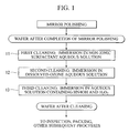
- This invention is an improvement on a cleaning method which is performed after mirror-polishing the surface of a silicon wafer, as shown in Fig. 1.
- the invention is characterized in comprising a first cleaning process, in which, after completion of the mirror polishing, the silicon wafer is immersed in a non-ionic surfactant aqueous solution; a second cleaning process, in which the wafer, after completion of the first cleaning process, is immersed in a dissolved-ozone aqueous solution; and, a third cleaning process, in which the wafer, after completion of the second cleaning process, is immersed in an aqueous solution containing ammonia and hydrogen peroxide; and is characterized in that the processes are performed in succession.
- the above cleaning method may be a cleaning method in which the surfactant concentration in the non-ionic surfactant aqueous solution used in the first cleaning process is between 0.001 and 10 weight percent.
- the above cleaning method may be a cleaning method in which the ozone concentration in the dissolved-ozone aqueous solution used in the second cleaning process is between 1 and 200 ppm.
- a silicon wafer cleaning method of this invention by performing in succession the first cleaning process through the third cleaning process, in this order, for a silicon wafer for which mirror polishing has been completed, in the first cleaning process polymer components contained in the polishing slurry used in the mirror polishing and remaining on the wafer surface, and organic contaminants existing on the wafer surface, are removed; in the second cleaning process, the surfactant used in the first cleaning process, as well as organic contaminants which could not be completely removed in the first cleaning process, are decomposed and removed; and in the third cleaning process, organic contaminants and metallic impurities are removed, so that a wafer with a high degree of cleanliness can be obtained.
- the object of a cleaning method of this invention is a silicon wafer after the surface has been mirror-polished. On the surface of this silicon wafer subjected to mirror-polishing there remain not only organic contaminants, metallic impurities, and other contaminants, but also components contained in the polishing slurry used in the mirror polishing process.
- the first cleaning process 11 through the third cleaning process 13 are performed in succession, as shown in Fig. 1.
- a silicon wafer which has been mirror-polished is immersed in a non-ionic surfactant aqueous solution.
- a non-ionic surfactant aqueous solution obtained by dissolving a non-ionic surfactant, which does not cause reactions on the wafer surface, in ultrapure water, is used.
- the surfactant concentration in the non-ionic surfactant aqueous solution used in the first cleaning process 11 is from 0.001 to 10 weight percent, and preferably from 0.1 to 3.0 weight percent, and more preferably 0.2 weight percent.
- the surfactant concentration is less than 0.001 weight percent, organic contaminants remaining on the wafer surface cannot be adequately removed; if the surfactant concentration exceeds 10 weight percent, a large amount of the surfactant adheres to the wafer surface, and there is difficulty in removing all of the adhering surfactant in the subsequent process.
- the non-ionic surfactant aqueous solution of the first cleaning process 11 is maintained in the temperature range from room temperature to 95°C. In the above temperature range, by heating the non-ionic surfactant aqueous solution to a temperature of 80 to 95°C and performing cleaning, the effect of cleaning and removing organic contaminants remaining on the wafer surface is enhanced, and so is advantageous.
- the time of immersion of the silicon wafer in the non-ionic surfactant aqueous solution is from 1 to 10 minutes, and preferably from 2 to 5 minutes. If the immersion time is less than 1 minute, cleaning and removal of organic contaminants cannot be said to be sufficient, whereas even if 10 minutes is exceeded the cleaning effect is unchanged, and efficiency is poor.
- non-ionic surfactant which is dissolved in the non-ionic surfactant aqueous solution
- examples of types of non-ionic surfactant which is dissolved in the non-ionic surfactant aqueous solution include sorbitan monolaurate, sorbitan sesqui-isostearate and other sorbitan fatty acid esters; glycerine monooleate, glycerine monoisostearate and other glycerine fatty acid esters; diglyceryl monooleate, decaglyceryl di-isostearate and other polyglyceryl fatty acid esters; polyoxyethylene sorbitan monooleate and other polyoxyethylene sorbitan fatty acid esters; polyoxyethylene sorbitol monolaurate, polyoxyethylene sorbitol tetraoleate, and other polyoxyethylene sorbitol fatty acid esters; polyoxyethylene glyceryl monooleate and other polyoxyethylene glyceryl fatty acid esters
- the wafer, having completed the above-described first cleaning process 11 is immersed in a dissolved-ozone aqueous solution.
- a dissolved-ozone aqueous solution By this means, the effect of dissolving and removing surfactant used in the first cleaning process 11, and organic contaminants not completely removed in the first cleaning process 11, is obtained.
- Cu, Ni, and other metallic impurities existing on the wafer surface are oxidized, and so can be easily removed in the following third cleaning process 13.
- the ozone concentration in the dissolved-ozone aqueous solution is from 1 to 20 ppm, and preferably from 5 to 20 ppm. If the ozone concentration is less than 1 ppm, the advantageous results of the second cleaning process 12 are not obtained.
- the upper limit of 20 ppm is set in view of selection of the cleaning device and other members.
- the dissolved-ozone aqueous solution in the second cleaning process 12 is used at a temperature approximately equal to room temperature. Or, a dissolved-ozone aqueous solution cooled to approximately 15°C, or a dissolved-ozone aqueous solution heated to approximately 50°C, may be used. Because it is easy to increase the ozone concentration in a dissolved-ozone aqueous solution which has been cooled, such a solution is used when ultrapure water of high purity, in which it is exceptionally difficult to raise the ozone concentration in aqueous solution, is employed as the solvent.
- the oxidizing power of dissolved-ozone aqueous solution which has been heated is greater than that at room temperature, and so is used when for example there is a need to increase the oxidizing power without changing the ozone concentration.
- the time of immersion of the silicon wafer in the dissolved-ozone aqueous solution is from 1 to 10 minutes, and preferably from 2 to 5 minutes. If the immersion time is less than 1 minute, cleaning and removal of organic contaminants cannot be said to be sufficient, whereas even if 10 minutes is exceeded the cleaning effect is unchanged, and efficiency is poor.
- the wafer having completed the above-described second cleaning process 12, is immersed in an aqueous solution containing ammonia and hydrogen peroxide.
- an aqueous solution containing ammonia and hydrogen peroxide used in the third cleaning process 13 may be employed.
- the aqueous solution containing ammonia and hydrogen peroxide used in the third cleaning process 13 is heated to a temperature of 75 to 80°C and used.
- the time of immersion of the silicon wafer in the aqueous solution containing ammonia and hydrogen peroxide is from 1 to 20 minutes, and preferable from 2 to 5 minutes. If the immersion time is less than 1 minute, cleaning and removal of particle components cannot be said to be sufficient, whereas even if 20 minutes is exceeded the cleaning effect is unchanged and efficiency is poor, and moreover roughening of the wafer surface may result.
- the order of the first cleaning process 11 through the third cleaning process 13 in the cleaning method of this invention is interchanged, with for example cleaning performed in the order of the third cleaning process 13, then the first cleaning process 11, and then the second cleaning process 12, then polymer components contained in the polishing slurry undergo dehydration condensation or other reactions due to the aqueous solution containing ammonia and hydrogen peroxide in the third cleaning process, so that derivatives of the polymer components are formed, and these derivatives adhere to the wafer surface, so that even when the first cleaning process and second cleaning process are performed after the third cleaning process, the derivatives cannot be removed, and the cleaning effect of the cleaning method of this invention is no longer obtained.
- each of the first cleaning process 11 through the third cleaning process 13 must be performed in succession, in this order.
- cleaning by immersion of the wafer into a low-pH acid liquid mixture may be further performed following the third cleaning process 13.
- a liquid mixture of hydrochloric acid and hydrogen peroxide may be used as the low-pH acid liquid mixture used here.
- alkaline ions and Al 3+ , Fe 2+ , Mg 2+ , and other cations which are insoluble in the aqueous solution containing ammonia and hydrogen peroxide used in the above third cleaning process, can be removed.
- non-ionic surfactant aqueous solution a non-ionic surfactant (model NCW, manufactured by Wako Pure Chemical Industries, Ltd.) was dissolved in ultrapure water, to prepare an aqueous solution with a concentration of 0.2 weight percent, and a silicon wafer was immersed in the non-ionic surfactant aqueous solution heated to 90°C and held for 3 minutes.
- a dissolved-ozone aqueous solution with ozone concentration 20 ppm was prepared, and the silicon wafer was immersed in the dissolved-ozone aqueous solution, held at room temperature, and held for 3 minutes.
- the silicon wafer was immersed and held for 3 minutes in an aqueous solution containing ammonia and hydrogen peroxide, prepared by dissolving 1.2 weight percent ammonia and 2.6 weight percent hydrogen peroxide in an aqueous solution heated to 80°C. After cleaning, the wafer was rinsed in pure water, and was then dried.
- an aqueous solution containing ammonia and hydrogen peroxide prepared by dissolving 1.2 weight percent ammonia and 2.6 weight percent hydrogen peroxide in an aqueous solution heated to 80°C. After cleaning, the wafer was rinsed in pure water, and was then dried.
- aqueous solution was prepared in which 1.2 weight percent ammonia and 2.6 weight percent hydrogen peroxide were dissolved, and a silicon wafer was immersed and held for 3 minutes in the aqueous solution containing ammonia and hydrogen peroxide, heated to 80°C. After cleaning, the wafer was rinsed with pure water and then dried.
- a particle counter (model CR80, manufactured by ADE) was used to measure the wafer surface over a fixed arbitrary range for silicon wafers which had been subjected to the cleaning of Embodiment 1 and the cleaning of Comparison Example 1, and particles exceeding 0.12 ⁇ m in size were detected.
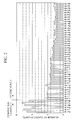
- the numbers of particles detected from wafers subjected to the cleaning of Embodiment 1 and Comparison Example 1 appear in Fig. 2; average values, maximum values, and minimum values for the numbers of particles detected from wafers subjected to the cleaning of Embodiment 1 and Comparison Example 1 are shown in Table 1.
- Table 1 Number of particles detected exceeding 0.12 ⁇ m Average value Maximum Minimum Embodiment 1 3.61 5.8 2.3 Comparison Example 1 11.9 13.2 10.2
- the cleaning method of this invention can be applied not only to silicon wafers which have been mirror-polished, but to cleaning of glass substrates for use in liquid crystal displays and similar.
Landscapes
- Chemical & Material Sciences (AREA)
- Chemical Kinetics & Catalysis (AREA)
- General Chemical & Material Sciences (AREA)
- Inorganic Chemistry (AREA)
- Life Sciences & Earth Sciences (AREA)
- Engineering & Computer Science (AREA)
- Oil, Petroleum & Natural Gas (AREA)
- Wood Science & Technology (AREA)
- Organic Chemistry (AREA)
- Cleaning Or Drying Semiconductors (AREA)
Abstract
Description
- The present invention relates to a silicon wafer cleaning method.
- Priority is claimed on
Japanese Patent Application No. 2005-231430, filed August 10, 2005 - In mirror-polishing of silicon wafers, the surface of a silicon wafer mounted on a holding jig is pressed with prescribed pressure against a polishing cloth fixed onto a turntable, and by rotating the turntable while supplying a polishing slurry between the polishing cloth and the wafer surface, the wafer surface is polished to a mirror finish. As the polishing slurry, normally a liquid prepared by suspending fine SiO2 particles or other abrasive particles in a weak alkaline liquid is used; cellulose or other polymer components may be further added to reduce haze and LPD, or to maintain wettability.
- After mirror-polishing, a silicon wafer is cleaned in order to remove particles, organic contaminants, metallic impurities and other contaminants which may exist on the surface. In general, the RCA method is used to clean silicon wafers after mirror polishing has been completed (see for example Non-Patent Reference 1: Fumio Shimura, Handoutai Shirikon Kesshougaku, Maruzen, Sept. 30 1993, pp. 125-127). The RCA method comprises two-stage cleaning using (1) a high-pH alkaline liquid mixture (hereafter "SC-1") based on hydrogen peroxide, and (2) a low-pH acidic liquid mixture (hereafter "SC-2"). By combining these liquid mixtures to perform cleaning, contaminants can be efficiently removed from the substrate surface.
- However, polymer components contained in the polishing slurry used in mirror polishing remain on the surface of a silicon wafer after the completion of mirror polishing, and when using the RCA cleaning described in the
above Non-Patent Reference 1, the polymer component contained in the polishing slurry undergoes a dehydration condensation or other reaction due to the SC-1 liquid mixture, to form derivatives of the polymer component; because this derivative is fixed on the wafer surface, the derivative fixed on the wafer surface is not removed even when SC-2 cleaning is performed following SC-1 cleaning, and so the cleanliness of the wafer surface cannot be improved sufficiently. - An object of this invention is the provision of a silicon wafer cleaning method with excellent cleaning performance.
- This invention is an improvement on a cleaning method which is performed after mirror-polishing the surface of a silicon wafer, as shown in Fig. 1. The invention is characterized in comprising a first cleaning process, in which, after completion of the mirror polishing, the silicon wafer is immersed in a non-ionic surfactant aqueous solution; a second cleaning process, in which the wafer, after completion of the first cleaning process, is immersed in a dissolved-ozone aqueous solution; and, a third cleaning process, in which the wafer, after completion of the second cleaning process, is immersed in an aqueous solution containing ammonia and hydrogen peroxide; and is characterized in that the processes are performed in succession.
- In the above cleaning method, by performing in succession the first cleaning process through the third cleaning process, in this order, for a silicon wafer for which mirror polishing has been completed, in the first cleaning process polymer components contained in the polishing slurry used in the mirror polishing and remaining on the wafer surface, and organic contaminants existing on the wafer surface, are removed; in the second cleaning process, the surfactant used in the first cleaning process, as well as organic contaminants which could not be completely removed in the first cleaning process, are decomposed and removed; and in the third cleaning process, organic contaminants and metallic impurities are removed, so that a wafer with a high degree of cleanliness can be obtained.
- The above cleaning method may be a cleaning method in which the surfactant concentration in the non-ionic surfactant aqueous solution used in the first cleaning process is between 0.001 and 10 weight percent.
- The above cleaning method may be a cleaning method in which the ozone concentration in the dissolved-ozone aqueous solution used in the second cleaning process is between 1 and 200 ppm.
- In a silicon wafer cleaning method of this invention, by performing in succession the first cleaning process through the third cleaning process, in this order, for a silicon wafer for which mirror polishing has been completed, in the first cleaning process polymer components contained in the polishing slurry used in the mirror polishing and remaining on the wafer surface, and organic contaminants existing on the wafer surface, are removed; in the second cleaning process, the surfactant used in the first cleaning process, as well as organic contaminants which could not be completely removed in the first cleaning process, are decomposed and removed; and in the third cleaning process, organic contaminants and metallic impurities are removed, so that a wafer with a high degree of cleanliness can be obtained.
-
- Fig. 1 shows cleaning processes of this invention, performed on a silicon wafer for which mirror polishing has been completed; and,
- Fig. 2 indicates the number of particles detected on a wafer after completion of cleaning, in
Embodiment 1 and in Comparison Example 1. - Next, preferred aspects for implementation of the invention are explained based on the drawings.
- The object of a cleaning method of this invention is a silicon wafer after the surface has been mirror-polished. On the surface of this silicon wafer subjected to mirror-polishing there remain not only organic contaminants, metallic impurities, and other contaminants, but also components contained in the polishing slurry used in the mirror polishing process.
- In the silicon wafer cleaning method of this invention, the
first cleaning process 11 through thethird cleaning process 13 are performed in succession, as shown in Fig. 1. - First, in the
first cleaning process 11, a silicon wafer which has been mirror-polished is immersed in a non-ionic surfactant aqueous solution. By this means, the advantageous result of cleaning and removal of polymer components and organic contaminants remaining on the wafer surface is obtained. In thisfirst cleaning process 11, a non-ionic surfactant aqueous solution, obtained by dissolving a non-ionic surfactant, which does not cause reactions on the wafer surface, in ultrapure water, is used. If an anionic surfactant or cationic surfactant or similar, other than a non-ionic surfactant, is used in the aqueous solution employed in thisfirst cleaning process 11, then there are cases in which reactions occur between the silicon and the surfactant, and there are problems in which the wafer surface is roughened. The surfactant concentration in the non-ionic surfactant aqueous solution used in thefirst cleaning process 11 is from 0.001 to 10 weight percent, and preferably from 0.1 to 3.0 weight percent, and more preferably 0.2 weight percent. If the surfactant concentration is less than 0.001 weight percent, organic contaminants remaining on the wafer surface cannot be adequately removed; if the surfactant concentration exceeds 10 weight percent, a large amount of the surfactant adheres to the wafer surface, and there is difficulty in removing all of the adhering surfactant in the subsequent process. - The non-ionic surfactant aqueous solution of the
first cleaning process 11 is maintained in the temperature range from room temperature to 95°C. In the above temperature range, by heating the non-ionic surfactant aqueous solution to a temperature of 80 to 95°C and performing cleaning, the effect of cleaning and removing organic contaminants remaining on the wafer surface is enhanced, and so is advantageous. The time of immersion of the silicon wafer in the non-ionic surfactant aqueous solution is from 1 to 10 minutes, and preferably from 2 to 5 minutes. If the immersion time is less than 1 minute, cleaning and removal of organic contaminants cannot be said to be sufficient, whereas even if 10 minutes is exceeded the cleaning effect is unchanged, and efficiency is poor. - Examples of types of non-ionic surfactant which is dissolved in the non-ionic surfactant aqueous solution include sorbitan monolaurate, sorbitan sesqui-isostearate and other sorbitan fatty acid esters; glycerine monooleate, glycerine monoisostearate and other glycerine fatty acid esters; diglyceryl monooleate, decaglyceryl di-isostearate and other polyglyceryl fatty acid esters; polyoxyethylene sorbitan monooleate and other polyoxyethylene sorbitan fatty acid esters; polyoxyethylene sorbitol monolaurate, polyoxyethylene sorbitol tetraoleate, and other polyoxyethylene sorbitol fatty acid esters; polyoxyethylene glyceryl monooleate and other polyoxyethylene glyceryl fatty acid esters; polyoxyethylene monoisostearate and other polyethylene glycol fatty acid esters; polyoxyethylene di-isostearate and other polyoxyglycol fatty acid esters; polyoxyethylene oleyl ether and other polyoxyethylene alkyl ethers; polyoxyethylene-1-polyoxypropylene-4-aklyl ether and other polyoxyethylene polyoxypropylene alkyl ethers; and polyoxyethylene castor oil, polyoxyethylene hydrogenated castor wax (40 E.O.), and other polyoxyethylene castor oils and hydrogenated castor waxes.
- Next, in the
second cleaning process 12, the wafer, having completed the above-describedfirst cleaning process 11, is immersed in a dissolved-ozone aqueous solution. By this means, the effect of dissolving and removing surfactant used in thefirst cleaning process 11, and organic contaminants not completely removed in thefirst cleaning process 11, is obtained. In addition, Cu, Ni, and other metallic impurities existing on the wafer surface are oxidized, and so can be easily removed in the followingthird cleaning process 13. The ozone concentration in the dissolved-ozone aqueous solution is from 1 to 20 ppm, and preferably from 5 to 20 ppm. If the ozone concentration is less than 1 ppm, the advantageous results of thesecond cleaning process 12 are not obtained. The upper limit of 20 ppm is set in view of selection of the cleaning device and other members. - The dissolved-ozone aqueous solution in the
second cleaning process 12 is used at a temperature approximately equal to room temperature. Or, a dissolved-ozone aqueous solution cooled to approximately 15°C, or a dissolved-ozone aqueous solution heated to approximately 50°C, may be used. Because it is easy to increase the ozone concentration in a dissolved-ozone aqueous solution which has been cooled, such a solution is used when ultrapure water of high purity, in which it is exceptionally difficult to raise the ozone concentration in aqueous solution, is employed as the solvent. The oxidizing power of dissolved-ozone aqueous solution which has been heated is greater than that at room temperature, and so is used when for example there is a need to increase the oxidizing power without changing the ozone concentration. The time of immersion of the silicon wafer in the dissolved-ozone aqueous solution is from 1 to 10 minutes, and preferably from 2 to 5 minutes. If the immersion time is less than 1 minute, cleaning and removal of organic contaminants cannot be said to be sufficient, whereas even if 10 minutes is exceeded the cleaning effect is unchanged, and efficiency is poor. - Next, in the
third cleaning process 13, the wafer, having completed the above-describedsecond cleaning process 12, is immersed in an aqueous solution containing ammonia and hydrogen peroxide. By this means, the effect of removing particles remaining on the wafer surface is obtained. Organic contaminants can be removed by means of the strong oxidizing power of hydrogen peroxide solution and the decomposing action of ammonia. Moreover, Au, Ag, Cu, Ni, Cd, Zn, Co, Cr, and other group 1B, group 2B, and other metallic impurities are removed through compound-generating reactions with ammonia. As the aqueous solution containing ammonia and hydrogen peroxide used in thethird cleaning process 13, an Sc-1 liquid mixture used in RCA cleaning may be employed. The aqueous solution containing ammonia and hydrogen peroxide used in thethird cleaning process 13 is heated to a temperature of 75 to 80°C and used. The time of immersion of the silicon wafer in the aqueous solution containing ammonia and hydrogen peroxide is from 1 to 20 minutes, and preferable from 2 to 5 minutes. If the immersion time is less than 1 minute, cleaning and removal of particle components cannot be said to be sufficient, whereas even if 20 minutes is exceeded the cleaning effect is unchanged and efficiency is poor, and moreover roughening of the wafer surface may result. - By thus performing the
first cleaning process 11 through the third cleaning process in succession, in this order, particles, organic contaminants, and metallic impurities remaining on the surface of a silicon wafer for which mirror polishing has been completed can be removed. - If, between each of the processes from the
first cleaning process 11 through the third cleaning process, rinsing is performed using pure water, then the cleaning effect of the following cleaning process cannot be fully realized due to the occurrence of non-ionic surfactant itself remaining on the wafer surface, and due to the occurrence of unevenness in the oxide film, formed by the dissolved-ozone aqueous solution, which results from introduction of OH bases; hence thefirst cleaning process 11 through thethird cleaning process 13 must be performed in succession. - If the order of the
first cleaning process 11 through thethird cleaning process 13 in the cleaning method of this invention is interchanged, with for example cleaning performed in the order of thethird cleaning process 13, then thefirst cleaning process 11, and then thesecond cleaning process 12, then polymer components contained in the polishing slurry undergo dehydration condensation or other reactions due to the aqueous solution containing ammonia and hydrogen peroxide in the third cleaning process, so that derivatives of the polymer components are formed, and these derivatives adhere to the wafer surface, so that even when the first cleaning process and second cleaning process are performed after the third cleaning process, the derivatives cannot be removed, and the cleaning effect of the cleaning method of this invention is no longer obtained. Further, if thefirst cleaning process 11 andsecond cleaning process 12 are interchanged, so that cleaning is performed in the order of thesecond cleaning process 12 and then thefirst cleaning process 11, the surfactant used in thefirst cleaning process 11 remains on the wafer surface, so that even if thethird cleaning process 13 is subsequently performed, adequate removal is not possible, and the cleaning effect of the cleaning method of this invention is not obtained. Hence in the cleaning method of this invention, each of thefirst cleaning process 11 through thethird cleaning process 13 must be performed in succession, in this order. - Further, in the cleaning method of this invention, cleaning by immersion of the wafer into a low-pH acid liquid mixture may be further performed following the
third cleaning process 13. As the low-pH acid liquid mixture used here, a liquid mixture of hydrochloric acid and hydrogen peroxide may be used. By means of a liquid mixture of hydrochloric acid and hydrogen peroxide, alkaline ions and Al3+, Fe2+, Mg2+, and other cations, which are insoluble in the aqueous solution containing ammonia and hydrogen peroxide used in the above third cleaning process, can be removed. - Next, an embodiment of the invention is explained in detail, together with a comparison example.
- The following cleaning was performed continuously on 1,320,000 silicon wafers manufactured at a rate of 30,000/month during the period from June 2001 to January 2005, and for which mirror polishing had been completed.
- First, as the non-ionic surfactant aqueous solution, a non-ionic surfactant (model NCW, manufactured by Wako Pure Chemical Industries, Ltd.) was dissolved in ultrapure water, to prepare an aqueous solution with a concentration of 0.2 weight percent, and a silicon wafer was immersed in the non-ionic surfactant aqueous solution heated to 90°C and held for 3 minutes. Next, a dissolved-ozone aqueous solution with ozone concentration 20 ppm was prepared, and the silicon wafer was immersed in the dissolved-ozone aqueous solution, held at room temperature, and held for 3 minutes. Next, the silicon wafer was immersed and held for 3 minutes in an aqueous solution containing ammonia and hydrogen peroxide, prepared by dissolving 1.2 weight percent ammonia and 2.6 weight percent hydrogen peroxide in an aqueous solution heated to 80°C. After cleaning, the wafer was rinsed in pure water, and was then dried.
- The following cleaning was performed continuously on 180,000 silicon wafers, manufactured under conditions similar to those of
Embodiment 1 at a rate of 30,000/month in the period from December 2000 to May 2001 and for which mirror polishing had been completed. - An aqueous solution was prepared in which 1.2 weight percent ammonia and 2.6 weight percent hydrogen peroxide were dissolved, and a silicon wafer was immersed and held for 3 minutes in the aqueous solution containing ammonia and hydrogen peroxide, heated to 80°C. After cleaning, the wafer was rinsed with pure water and then dried.
- A particle counter (model CR80, manufactured by ADE) was used to measure the wafer surface over a fixed arbitrary range for silicon wafers which had been subjected to the cleaning of
Embodiment 1 and the cleaning of Comparison Example 1, and particles exceeding 0.12 µm in size were detected. The numbers of particles detected from wafers subjected to the cleaning ofEmbodiment 1 and Comparison Example 1 appear in Fig. 2; average values, maximum values, and minimum values for the numbers of particles detected from wafers subjected to the cleaning ofEmbodiment 1 and Comparison Example 1 are shown in Table 1.Table 1 Number of particles detected exceeding 0.12µm Average value Maximum Minimum Embodiment 1 3.61 5.8 2.3 Comparison Example 1 11.9 13.2 10.2 - As is clear from Fig. 2 and Table 1, compared with wafers subjected to the cleaning of Comparison Example 1, the number of particles exceeding 0.12 µm detected on the wafers subjected to the cleaning of
Embodiment 1 is much smaller, and so it is seen that the cleanliness of wafers can be improved by means of the cleaning method of this invention. - The cleaning method of this invention can be applied not only to silicon wafers which have been mirror-polished, but to cleaning of glass substrates for use in liquid crystal displays and similar.
- In the above, a preferred embodiment of the invention was explained; but this invention is not limited to the embodiment. Various additions, omissions, replacements, and other alterations can be made, without deviating from the gist of the invention. The invention is not limited by the above explanation, but is limited only by the scope of the attached claims.
Claims (3)
- A silicon wafer cleaning method, performed after mirror-polishing of the surface of the silicon wafer, comprising:a first cleaning process, in which, after completion of said mirror polishing, the silicon wafer is immersed in a non-ionic surfactant aqueous solution;a second cleaning process, in which the silicon wafer, after completion of said first cleaning process, is immersed in a dissolved-ozone aqueous solution; and,a third cleaning process, in which the silicon wafer, after completion of said second cleaning process, is immersed in an aqueous solution containing ammonia and hydrogen peroxide;and whereinsaid first cleaning process through third cleaning process are performed in succession.
- The cleaning method according to Claim 1, wherein the surfactant concentration in the non-ionic surfactant aqueous solution used in said first cleaning process is from 0.001 to 10 weight percent.
- The cleaning method according to Claim 1, wherein the ozone concentration in the dissolved-ozone aqueous solution used in said second cleaning process is from 1 to 20 ppm.
Applications Claiming Priority (1)
| Application Number | Priority Date | Filing Date | Title |
|---|---|---|---|
| JP2005231430A JP4613744B2 (en) | 2005-08-10 | 2005-08-10 | Cleaning method of silicon wafer |
Publications (3)
| Publication Number | Publication Date |
|---|---|
| EP1753015A2 true EP1753015A2 (en) | 2007-02-14 |
| EP1753015A3 EP1753015A3 (en) | 2008-08-20 |
| EP1753015B1 EP1753015B1 (en) | 2016-11-23 |
Family
ID=37489519
Family Applications (1)
| Application Number | Title | Priority Date | Filing Date |
|---|---|---|---|
| EP06016243.5A Active EP1753015B1 (en) | 2005-08-10 | 2006-08-03 | Silicon wafer cleaning method |
Country Status (5)
| Country | Link |
|---|---|
| US (1) | US7632357B2 (en) |
| EP (1) | EP1753015B1 (en) |
| JP (1) | JP4613744B2 (en) |
| CN (1) | CN100423190C (en) |
| TW (1) | TWI317974B (en) |
Cited By (2)
| Publication number | Priority date | Publication date | Assignee | Title |
|---|---|---|---|---|
| US10121649B2 (en) | 2008-12-04 | 2018-11-06 | Siltronic Ag | Cleaning method of semiconductor wafer |
| US20240120192A1 (en) * | 2021-03-09 | 2024-04-11 | Shin-Etsu Handotai Co., Ltd. | Method of cleaning silicon wafer, method of manufacturing silicon wafer, and silicon wafer |
Families Citing this family (15)
| Publication number | Priority date | Publication date | Assignee | Title |
|---|---|---|---|---|
| US20100129996A1 (en) * | 2008-04-28 | 2010-05-27 | Jian Zhong Yuan | Silicon material surface etching for large grain polysilicon thin film deposition and structure |
| US7700535B1 (en) * | 2009-01-12 | 2010-04-20 | Ppt Research | Wafer/Ingot cleaning in wire saw cutting comprising an ethoxylated alcohol/polyalkylsiloxane mixture |
| US8845812B2 (en) * | 2009-06-12 | 2014-09-30 | Micron Technology, Inc. | Method for contamination removal using magnetic particles |
| JP2012531734A (en) * | 2009-06-25 | 2012-12-10 | ラム・リサーチ・アーゲー | Method for processing a semiconductor wafer |
| JP5458857B2 (en) * | 2009-12-14 | 2014-04-02 | 株式会社Sumco | Cleaning method |
| JP5289411B2 (en) | 2010-10-27 | 2013-09-11 | 富士フイルム株式会社 | Multi-agent type semiconductor substrate cleaning agent, cleaning method using the same, and semiconductor device manufacturing method |
| CN102368468B (en) * | 2011-10-17 | 2013-09-25 | 浙江贝盛光伏股份有限公司 | Precleaning process of silicon wafer |
| WO2018055941A1 (en) * | 2016-09-21 | 2018-03-29 | 株式会社フジミインコーポレーテッド | Surface treatment composition |
| CN108499963A (en) * | 2017-05-18 | 2018-09-07 | 苏州权素船舶电子有限公司 | A kind of electronic material ground and cleaned method |
| CN109427543B (en) * | 2017-08-31 | 2022-09-23 | 胜高股份有限公司 | Method for cleaning silicon wafer |
| JP7138432B2 (en) * | 2017-12-26 | 2022-09-16 | 花王株式会社 | Silicon wafer manufacturing method |
| JP2019121795A (en) * | 2017-12-27 | 2019-07-22 | 花王株式会社 | Manufacturing method of silicon wafer |
| JP2020155721A (en) * | 2019-03-22 | 2020-09-24 | 株式会社Screenホールディングス | Substrate processing method |
| CN113130301B (en) * | 2021-04-15 | 2023-09-22 | 通威太阳能(安徽)有限公司 | A method to solve the alkali polishing EL airflow printing of single crystal PERC cells |
| CN113555274B (en) * | 2021-07-21 | 2023-06-02 | 江西圆融光电科技有限公司 | Chip cleaning method |
Family Cites Families (13)
| Publication number | Priority date | Publication date | Assignee | Title |
|---|---|---|---|---|
| US5695572A (en) * | 1994-08-25 | 1997-12-09 | Wacker Siltronic Gesellschaft Fur Halbleitermaterialien Aktiengesellschaft | Cleaning agent and method for cleaning semiconductor wafers |
| JPH08195369A (en) * | 1995-01-13 | 1996-07-30 | Daikin Ind Ltd | Substrate cleaning method |
| JP3198899B2 (en) * | 1995-11-30 | 2001-08-13 | アルプス電気株式会社 | Wet treatment method |
| US6245155B1 (en) | 1996-09-06 | 2001-06-12 | Arch Specialty Chemicals, Inc. | Method for removing photoresist and plasma etch residues |
| US5932022A (en) * | 1998-04-21 | 1999-08-03 | Harris Corporation | SC-2 based pre-thermal treatment wafer cleaning process |
| JP2000091291A (en) | 1998-09-11 | 2000-03-31 | Memc Kk | Washing method of silicon wafer |
| US6230720B1 (en) * | 1999-08-16 | 2001-05-15 | Memc Electronic Materials, Inc. | Single-operation method of cleaning semiconductors after final polishing |
| US7456113B2 (en) * | 2000-06-26 | 2008-11-25 | Applied Materials, Inc. | Cleaning method and solution for cleaning a wafer in a single wafer process |
| JP2002100599A (en) * | 2000-09-21 | 2002-04-05 | Mitsubishi Materials Silicon Corp | Washing method for silicon wafer |
| US6861007B2 (en) * | 2001-03-02 | 2005-03-01 | Micron Technology, Inc. | Method for removing organic material from a substrate and for oxidizing oxidizable material thereon |
| TWI302950B (en) * | 2002-01-28 | 2008-11-11 | Mitsubishi Chem Corp | Cleaning solution and method of cleanimg board of semiconductor device |
| JP4026384B2 (en) * | 2002-03-22 | 2007-12-26 | 株式会社Sumco | Semiconductor substrate cleaning method |
| JP4232002B2 (en) * | 2003-01-16 | 2009-03-04 | 日本電気株式会社 | Cleaning composition for device substrate, cleaning method and cleaning apparatus using the cleaning composition |
-
2005
- 2005-08-10 JP JP2005231430A patent/JP4613744B2/en not_active Expired - Lifetime
-
2006
- 2006-08-02 TW TW095128352A patent/TWI317974B/en active
- 2006-08-03 EP EP06016243.5A patent/EP1753015B1/en active Active
- 2006-08-04 US US11/499,142 patent/US7632357B2/en active Active
- 2006-08-08 CN CNB2006101592416A patent/CN100423190C/en active Active
Cited By (2)
| Publication number | Priority date | Publication date | Assignee | Title |
|---|---|---|---|---|
| US10121649B2 (en) | 2008-12-04 | 2018-11-06 | Siltronic Ag | Cleaning method of semiconductor wafer |
| US20240120192A1 (en) * | 2021-03-09 | 2024-04-11 | Shin-Etsu Handotai Co., Ltd. | Method of cleaning silicon wafer, method of manufacturing silicon wafer, and silicon wafer |
Also Published As
| Publication number | Publication date |
|---|---|
| CN1913102A (en) | 2007-02-14 |
| EP1753015B1 (en) | 2016-11-23 |
| TW200709292A (en) | 2007-03-01 |
| CN100423190C (en) | 2008-10-01 |
| TWI317974B (en) | 2009-12-01 |
| US7632357B2 (en) | 2009-12-15 |
| JP4613744B2 (en) | 2011-01-19 |
| EP1753015A3 (en) | 2008-08-20 |
| US20070034229A1 (en) | 2007-02-15 |
| JP2007048918A (en) | 2007-02-22 |
Similar Documents
| Publication | Publication Date | Title |
|---|---|---|
| EP1753015B1 (en) | Silicon wafer cleaning method | |
| US6194366B1 (en) | Post chemical-mechanical planarization (CMP) cleaning composition | |
| US6537916B2 (en) | Removal of CMP residue from semiconductor substrate using supercritical carbon dioxide process | |
| CN1107343C (en) | Cleaning wafer substrates of metal contamination while maintaining wafer smoothness | |
| JP4350364B2 (en) | Cleaning composition, semiconductor wafer cleaning method and manufacturing method | |
| KR101520917B1 (en) | Texturing and cleaning agent for the surface treatment of wafers and use thereof | |
| US20090056744A1 (en) | Wafer cleaning compositions and methods | |
| KR101697659B1 (en) | Semiconductor wafer cleaning method | |
| KR101005925B1 (en) | Semiconductor Substrate Cleaning Liquid Composition | |
| CN116631848A (en) | A method for cleaning silicon wafers to improve the quality of metal and particles on the surface of silicon polished wafers | |
| US5964953A (en) | Post-etching alkaline treatment process | |
| CN113736580A (en) | A mixed acid cleaning solution for cleaning and polishing silicon wafers and a cleaning method for polishing silicon wafers | |
| KR100789776B1 (en) | Cleaning agent composition, method for cleaning and use thereof | |
| JP4857738B2 (en) | Semiconductor wafer cleaning method and manufacturing method | |
| CN113544248B (en) | Semiconductor wafer cleaning liquid composition and cleaning method using the same | |
| KR20070018689A (en) | Silicon Wafer Cleaning Method | |
| KR20080075508A (en) | Plane grinding method and manufacturing method of semiconductor wafer | |
| JP3257518B2 (en) | How to store silicon wafers in liquid | |
| US20140096793A1 (en) | Uv treatment of polished wafers | |
| TW201528350A (en) | Fitting wafer manufacturing method | |
| CN117352372A (en) | A method for cleaning silicon carbide wafers | |
| KR100679008B1 (en) | Cleaning composition for semiconductor device | |
| US6416391B1 (en) | Method of demounting silicon wafers after polishing | |
| JP2006134906A (en) | Silicon wafer storage method | |
| KR20100137728A (en) | Organic pollutant cleaning liquid and solar cell wafer cleaning method using the same |
Legal Events
| Date | Code | Title | Description |
|---|---|---|---|
| PUAI | Public reference made under article 153(3) epc to a published international application that has entered the european phase |
Free format text: ORIGINAL CODE: 0009012 |
|
| 17P | Request for examination filed |
Effective date: 20060803 |
|
| AK | Designated contracting states |
Kind code of ref document: A2 Designated state(s): AT BE BG CH CY CZ DE DK EE ES FI FR GB GR HU IE IS IT LI LT LU LV MC NL PL PT RO SE SI SK TR |
|
| AX | Request for extension of the european patent |
Extension state: AL BA HR MK YU |
|
| PUAL | Search report despatched |
Free format text: ORIGINAL CODE: 0009013 |
|
| AK | Designated contracting states |
Kind code of ref document: A3 Designated state(s): AT BE BG CH CY CZ DE DK EE ES FI FR GB GR HU IE IS IT LI LT LU LV MC NL PL PT RO SE SI SK TR |
|
| AX | Request for extension of the european patent |
Extension state: AL BA HR MK RS |
|
| 17Q | First examination report despatched |
Effective date: 20081202 |
|
| AKX | Designation fees paid |
Designated state(s): DE FR |
|
| REG | Reference to a national code |
Ref country code: DE Ref legal event code: R079 Ref document number: 602006050983 Country of ref document: DE Free format text: PREVIOUS MAIN CLASS: H01L0021020000 Ipc: H01L0021306000 |
|
| GRAP | Despatch of communication of intention to grant a patent |
Free format text: ORIGINAL CODE: EPIDOSNIGR1 |
|
| RIC1 | Information provided on ipc code assigned before grant |
Ipc: H01L 21/306 20060101AFI20160601BHEP Ipc: B08B 3/08 20060101ALI20160601BHEP Ipc: C11D 11/00 20060101ALI20160601BHEP Ipc: C11D 3/39 20060101ALI20160601BHEP |
|
| INTG | Intention to grant announced |
Effective date: 20160616 |
|
| GRAS | Grant fee paid |
Free format text: ORIGINAL CODE: EPIDOSNIGR3 |
|
| GRAA | (expected) grant |
Free format text: ORIGINAL CODE: 0009210 |
|
| AK | Designated contracting states |
Kind code of ref document: B1 Designated state(s): DE FR |
|
| REG | Reference to a national code |
Ref country code: DE Ref legal event code: R096 Ref document number: 602006050983 Country of ref document: DE |
|
| REG | Reference to a national code |
Ref country code: FR Ref legal event code: PLFP Year of fee payment: 12 |
|
| REG | Reference to a national code |
Ref country code: DE Ref legal event code: R097 Ref document number: 602006050983 Country of ref document: DE |
|
| PLBE | No opposition filed within time limit |
Free format text: ORIGINAL CODE: 0009261 |
|
| STAA | Information on the status of an ep patent application or granted ep patent |
Free format text: STATUS: NO OPPOSITION FILED WITHIN TIME LIMIT |
|
| 26N | No opposition filed |
Effective date: 20170824 |
|
| REG | Reference to a national code |
Ref country code: FR Ref legal event code: PLFP Year of fee payment: 13 |
|
| PGFP | Annual fee paid to national office [announced via postgrant information from national office to epo] |
Ref country code: DE Payment date: 20250820 Year of fee payment: 20 |
|
| PGFP | Annual fee paid to national office [announced via postgrant information from national office to epo] |
Ref country code: FR Payment date: 20250828 Year of fee payment: 20 |
|
| REG | Reference to a national code |
Ref country code: DE Ref legal event code: R079 Ref document number: 602006050983 Country of ref document: DE Free format text: PREVIOUS MAIN CLASS: H01L0021306000 Ipc: H10P0050000000 |