EP1748502A1 - Semiconductor device and process for producing same - Google Patents
Semiconductor device and process for producing same Download PDFInfo
- Publication number
- EP1748502A1 EP1748502A1 EP06013356A EP06013356A EP1748502A1 EP 1748502 A1 EP1748502 A1 EP 1748502A1 EP 06013356 A EP06013356 A EP 06013356A EP 06013356 A EP06013356 A EP 06013356A EP 1748502 A1 EP1748502 A1 EP 1748502A1
- Authority
- EP
- European Patent Office
- Prior art keywords
- substrate
- depression pattern
- printing
- semiconductor device
- application
- Prior art date
- Legal status (The legal status is an assumption and is not a legal conclusion. Google has not performed a legal analysis and makes no representation as to the accuracy of the status listed.)
- Granted
Links
Images



Classifications
-
- B—PERFORMING OPERATIONS; TRANSPORTING
- B82—NANOTECHNOLOGY
- B82Y—SPECIFIC USES OR APPLICATIONS OF NANOSTRUCTURES; MEASUREMENT OR ANALYSIS OF NANOSTRUCTURES; MANUFACTURE OR TREATMENT OF NANOSTRUCTURES
- B82Y10/00—Nanotechnology for information processing, storage or transmission, e.g. quantum computing or single electron logic
-
- B—PERFORMING OPERATIONS; TRANSPORTING
- B82—NANOTECHNOLOGY
- B82Y—SPECIFIC USES OR APPLICATIONS OF NANOSTRUCTURES; MEASUREMENT OR ANALYSIS OF NANOSTRUCTURES; MANUFACTURE OR TREATMENT OF NANOSTRUCTURES
- B82Y40/00—Manufacture or treatment of nanostructures
-
- H—ELECTRICITY
- H05—ELECTRIC TECHNIQUES NOT OTHERWISE PROVIDED FOR
- H05K—PRINTED CIRCUITS; CASINGS OR CONSTRUCTIONAL DETAILS OF ELECTRIC APPARATUS; MANUFACTURE OF ASSEMBLAGES OF ELECTRICAL COMPONENTS
- H05K3/00—Apparatus or processes for manufacturing printed circuits
- H05K3/10—Apparatus or processes for manufacturing printed circuits in which conductive material is applied to the insulating support in such a manner as to form the desired conductive pattern
- H05K3/12—Apparatus or processes for manufacturing printed circuits in which conductive material is applied to the insulating support in such a manner as to form the desired conductive pattern using thick film techniques, e.g. printing techniques to apply the conductive material or similar techniques for applying conductive paste or ink patterns
- H05K3/1258—Apparatus or processes for manufacturing printed circuits in which conductive material is applied to the insulating support in such a manner as to form the desired conductive pattern using thick film techniques, e.g. printing techniques to apply the conductive material or similar techniques for applying conductive paste or ink patterns by using a substrate provided with a shape pattern, e.g. grooves, banks, resist pattern
-
- H—ELECTRICITY
- H10—SEMICONDUCTOR DEVICES; ELECTRIC SOLID-STATE DEVICES NOT OTHERWISE PROVIDED FOR
- H10K—ORGANIC ELECTRIC SOLID-STATE DEVICES
- H10K10/00—Organic devices specially adapted for rectifying, amplifying, oscillating or switching; Organic capacitors or resistors having potential barriers
- H10K10/40—Organic transistors
- H10K10/46—Field-effect transistors, e.g. organic thin-film transistors [OTFT]
- H10K10/462—Insulated gate field-effect transistors [IGFETs]
- H10K10/464—Lateral top-gate IGFETs comprising only a single gate
-
- H—ELECTRICITY
- H10—SEMICONDUCTOR DEVICES; ELECTRIC SOLID-STATE DEVICES NOT OTHERWISE PROVIDED FOR
- H10K—ORGANIC ELECTRIC SOLID-STATE DEVICES
- H10K10/00—Organic devices specially adapted for rectifying, amplifying, oscillating or switching; Organic capacitors or resistors having potential barriers
- H10K10/40—Organic transistors
- H10K10/46—Field-effect transistors, e.g. organic thin-film transistors [OTFT]
- H10K10/462—Insulated gate field-effect transistors [IGFETs]
- H10K10/466—Lateral bottom-gate IGFETs comprising only a single gate
-
- H—ELECTRICITY
- H10—SEMICONDUCTOR DEVICES; ELECTRIC SOLID-STATE DEVICES NOT OTHERWISE PROVIDED FOR
- H10K—ORGANIC ELECTRIC SOLID-STATE DEVICES
- H10K71/00—Manufacture or treatment specially adapted for the organic devices covered by this subclass
- H10K71/10—Deposition of organic active material
- H10K71/12—Deposition of organic active material using liquid deposition, e.g. spin coating
- H10K71/13—Deposition of organic active material using liquid deposition, e.g. spin coating using printing techniques, e.g. ink-jet printing or screen printing
-
- H—ELECTRICITY
- H10—SEMICONDUCTOR DEVICES; ELECTRIC SOLID-STATE DEVICES NOT OTHERWISE PROVIDED FOR
- H10K—ORGANIC ELECTRIC SOLID-STATE DEVICES
- H10K71/00—Manufacture or treatment specially adapted for the organic devices covered by this subclass
- H10K71/10—Deposition of organic active material
- H10K71/12—Deposition of organic active material using liquid deposition, e.g. spin coating
- H10K71/13—Deposition of organic active material using liquid deposition, e.g. spin coating using printing techniques, e.g. ink-jet printing or screen printing
- H10K71/135—Deposition of organic active material using liquid deposition, e.g. spin coating using printing techniques, e.g. ink-jet printing or screen printing using ink-jet printing
-
- H—ELECTRICITY
- H10—SEMICONDUCTOR DEVICES; ELECTRIC SOLID-STATE DEVICES NOT OTHERWISE PROVIDED FOR
- H10K—ORGANIC ELECTRIC SOLID-STATE DEVICES
- H10K71/00—Manufacture or treatment specially adapted for the organic devices covered by this subclass
- H10K71/60—Forming conductive regions or layers, e.g. electrodes
- H10K71/611—Forming conductive regions or layers, e.g. electrodes using printing deposition, e.g. ink jet printing
-
- H—ELECTRICITY
- H10—SEMICONDUCTOR DEVICES; ELECTRIC SOLID-STATE DEVICES NOT OTHERWISE PROVIDED FOR
- H10K—ORGANIC ELECTRIC SOLID-STATE DEVICES
- H10K71/00—Manufacture or treatment specially adapted for the organic devices covered by this subclass
- H10K71/821—Patterning of a layer by embossing, e.g. stamping to form trenches in an insulating layer
-
- G—PHYSICS
- G03—PHOTOGRAPHY; CINEMATOGRAPHY; ANALOGOUS TECHNIQUES USING WAVES OTHER THAN OPTICAL WAVES; ELECTROGRAPHY; HOLOGRAPHY
- G03F—PHOTOMECHANICAL PRODUCTION OF TEXTURED OR PATTERNED SURFACES, e.g. FOR PRINTING, FOR PROCESSING OF SEMICONDUCTOR DEVICES; MATERIALS THEREFOR; ORIGINALS THEREFOR; APPARATUS SPECIALLY ADAPTED THEREFOR
- G03F7/00—Photomechanical, e.g. photolithographic, production of textured or patterned surfaces, e.g. printing surfaces; Materials therefor, e.g. comprising photoresists; Apparatus specially adapted therefor
- G03F7/0002—Lithographic processes using patterning methods other than those involving the exposure to radiation, e.g. by stamping
-
- H—ELECTRICITY
- H05—ELECTRIC TECHNIQUES NOT OTHERWISE PROVIDED FOR
- H05K—PRINTED CIRCUITS; CASINGS OR CONSTRUCTIONAL DETAILS OF ELECTRIC APPARATUS; MANUFACTURE OF ASSEMBLAGES OF ELECTRICAL COMPONENTS
- H05K2203/00—Indexing scheme relating to apparatus or processes for manufacturing printed circuits covered by H05K3/00
- H05K2203/01—Tools for processing; Objects used during processing
- H05K2203/0104—Tools for processing; Objects used during processing for patterning or coating
- H05K2203/013—Inkjet printing, e.g. for printing insulating material or resist
Definitions
- the present invention contains subject matter related to Japanese Patent Application JP 2005-218224 filed in the Japanese Patent Office on July 28, 2005 , the entire contents of which are incorporated herein by reference.
- the present invention relates to semiconductor devices and processes for producing semiconductor devices.
- the present invention relates to a process for producing a semiconductor device, the process including forming a pattern by printing.
- the present invention also relates to a semiconductor device produced by the process.
- semiconductor devices including active layers containing organic semiconductor materials have been receiving attention.
- a semiconductor device including the organic semiconductor material it is possible to form the active layer composed of the organic semiconductor material by application at a low temperature.
- the semiconductor device including the organic semiconductor material has an advantage in view of cost reduction.
- the semiconductor device can be formed on a low-heat-resistant flexible substrate, such as a plastic substrate.
- a gate insulating film, a source electrode, a drain electrode, and a gate electrode in addition to the active layer can be formed by patterning using printing with application materials, thus leading to further cost reduction.
- An inkjet printing has been studied as a method for forming a pattern with such an application material.
- Various materials can be applied by the inkjet printing as long as the materials each have a viscosity of several centipoises.
- printing precision is about 20 ⁇ m at the present time.
- a method for forming banks composed of polyimide or the like at the periphery of a position into which the ink is discharged has been proposed.
- the process may provide a high-precision fine pattern by printing to achieve higher chip density without leading to the complication of the production process. It is also desirable to provide a semiconductor device obtained by the production process.
- a process for producing a semiconductor device including a first embossing step of pressing a stamp having a relief pattern onto a surface of a substrate to form a depression pattern on the surface of the substrate; a second step of feeding an application material composed of a semiconductor material or a conductive material into the depression pattern by printing; and a third step of curing the application material fed by printing. Furthermore, according to another embodiment of the present invention, there is provided a semiconductor device obtained by the production process.
- the depression pattern is formed by embossing with the stamp prepared, the depression pattern is formed through only a single step. That is, the depression pattern is formed through a smaller number of steps compared with the case of forming banks on a substrate.
- the second step since the application material is fed into the depression pattern by printing, the extension of the application material on the substrate is limited. Thus, the application material is fed by printing into the depression pattern with satisfactory position accuracy and form accuracy and then cured to form a layer composed of the semiconductor material or the conductive material.
- Figs. 1A to 1E are each a cross-sectional process drawing illustrating a production process according to a first embodiment.
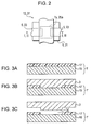
- Fig. 2 is a plan view of a thin-film transistor produced according to the first embodiment. The first embodiment in which a top-gate thin-film transistor is produced by a process according to an embodiment of the present invention will be described on the basis of the cross-sectional process drawings shown in Figs. 1A to 1E while referring to Fig. 2.
- a stamp 3 having a relief pattern on a surface thereof is pressed against a substrate 1 to form a depression pattern 1a.
- a surface of the substrate 1 is processed by embossing to form the depression pattern 1a.
- the depression pattern 1a has the shape of an active layer in the thin-film transistor to be produced in this embodiment and is in the form of a rectangle.
- the substrate 1 is a plastic substrate composed of, for example, a polyethylene terephthalate (PET), a polyether sulfone (PES), or a polyethylene naphthalate (PEN).
- the substrate 1 may be a plastic substrate or a glass substrate having a buffer layer composed of a resin material that is easily processed by embossing. When the substrate 1 has the buffer layer on a surface thereof, the buffer layer is subjected to embossing to form the depression pattern 1a.
- the stamp 3 has a protrusion pattern corresponding to the depression pattern 1a, the protrusion pattern being disposed on a main surface thereof.
- the stamp 3 is composed of a material having a softening temperature or a glass transition temperature higher than that of the substrate 1 or the buffer layer constituting the surface layer.
- the temperature of the substrate 1 is increased to a temperature higher than the softening temperature or the glass transition temperature of the surface layer of the substrate 1 while the stamp 3 is being pressed onto a surface of the substrate 1. This forces the protrusion portion of the stamp 3 into the surface layer of the substrate 1.
- the substrate 1 is cooled to cure while the stamp 3 is being pressed. Then, the stamp 3 is detached from the substrate 1.
- source/drain electrodes 5 are formed by patterning so as to be in contact with both edges of the depression pattern 1a.
- the source/drain electrodes 5 is formed by, for example, printing, such as inkjet printing, microcontact printing, or a screen printing, or photolithography.
- the source/drain electrodes 5 are formed by printing.
- printing with a paste or a liquid application material containing a conductive material is employed. That is, the application material is applied in a pattern by printing and then solidified to form the source/drain electrodes 5.
- a formed electrode material layer is pattern-etched with a resist pattern as a mask, the resist pattern being formed by lithography.
- the electrode material layer disposed on the resist pattern is removed together with the resist pattern by a lift-off method.
- the electrode material layer is formed by application.
- an application material 7 containing an organic semiconductor material is fed into the depression pattern 1a by printing through the tip of an application nozzle.
- the application material 7 is fed into the depression pattern 1a by being dropped through the tip of the application nozzle using inkjet printing, dispensing, or the like.
- the volume of the liquid application material 7 containing the organic semiconductor material dissolved in a solvent is substantially equal to the capacity of the depression pattern 1a.
- the application material 7 fed by printing is solidified to form an active layer 7a composed of the organic semiconductor material.
- the solvent in the liquid application material 7 is removed by evaporation to solidify the application material 7, resulting in the active layer 7a.
- the volume of the application material 7 fed by printing is substantially equal to the capacity of the depression pattern 1a, and then the application material 7 is solidified.
- the height of the surface of the active layer 7a is substantially the same as that of the surface of the substrate 1.
- the active layer 7a is in contact with the source/drain electrodes 5 at the side walls of the depression pattern 1a.
- the formation of the source/drain electrodes 5 described with reference to Fig. 1B and the formation of the active layer 7a described with reference to Fig. 1C may be performed in inverse order as long as damage to the active layer 7a is prevented.
- the formation steps are performed in inverse order, and the height of the surface of the active layer 7a formed by printing is higher than that of the surface of the substrate 1, if necessary, the active layer 7a may be planarized by polishing in such a way that the height of the surface of the active layer 7a is substantially the same as that of the surface of the substrate 1, and then the source/drain electrodes 5 may be formed.
- a gate insulating film 9 is formed on the substrate 1 by an application method, such as spin coating or slit coating, so as to cover the active layer 7a and the source/drain electrodes 5.
- an application method such as spin coating or slit coating
- a gate electrode 11 is formed on the gate insulating film 9 and over the active layer 7a between the source/drain electrodes 5.
- the gate electrode 11 is formed by printing, such as inkjet printing, microcontact printing, or screen printing, or photolithography as the method for forming the source/drain electrodes 5 illustrated with reference to Fig. 1B.
- a top-gate thin-film transistor is produced as a semiconductor device 13.
- the semiconductor device 13 includes the active layer 7a composed of an organic semiconductor material and formed by solidifying the application material; and the depression pattern 1a disposed at the surface of the substrate 1, the depression pattern 1a being selectively filled with the active layer 7a.
- the depression pattern 1a is formed by embossing with a single stamp 3
- the depression pattern 1a is formed through only a single step. That is, the depression pattern 1a can be formed through a smaller number of steps compared with the case of forming banks on a substrate to form a depression pattern.
- the application material is fed by printing into the depression pattern 1a formed by embossing, the extension of the application material on the substrate is limited.
- the application material 7 can be applied by printing into the depression pattern 1a with satisfactory position accuracy and form accuracy.
- the active layer 7a can be formed with high precision by printing without leading to the complication of the production process. Therefore, it is possible to achieve higher levels of integration of the semiconductor device 13 (thin-film transistor) including the active layer 7a.
- Figs. 3A to 3C are each a cross-sectional process drawing illustrating a production process according to a second embodiment.
- the differences between the second embodiment and the first embodiment are the structure of a substrate 1' and a procedure for forming a depression pattern 1a'.
- the subsequent steps are the same as those in the first embodiment.
- the substrate 1' including a resin material layer 17 disposed on a material substrate 15 is prepared.
- the material substrate 15 is a plastic substrate, a glass substrate, or the like.
- the resin material layer 17 is composed of an ultraviolet-curable resin or a thermosetting resin and is provided in an uncured state by an application method.
- the stamp 3 is pressed onto the surface of the substrate 1'.
- the same stamp 3 as that in the first embodiment may be used.
- the uncured resin material layer 17 is cured while the stamp 3 is being pressed.
- the resin material layer 17 is composed of an ultraviolet-curable resin
- the resin material layer 17 is irradiated with ultraviolet rays from the transparent component side of the stamp 3 and material substrate 15, thereby curing the resin material layer 17.
- the resin material layer 17 is composed of a thermosetting resin
- the resin material layer 17 is cured by heating.
- the stamp 3 is detached from the substrate 1'.
- the depression pattern 1a' corresponding to the protrusion pattern of the stamp 3 is formed at the surface of the substrate 1'.
- the depression pattern 1a' is formed by embossing, and then an application material is fed by printing into the depression pattern 1a' to form an active layer. Therefore, it is possible to form the active layer with high precision by printing without leading to the complication of the production process, as in the first embodiment.
- the resin material layer 17 described in Fig. 3A is composed of an ultraviolet-curable resin
- the material substrate 15 constituting the substrate 1' is not stressed by heat.
- a material having low resistance to heat can be used as the material substrate 15.
- Figs. 4A to 4E are each a cross-sectional process drawing illustrating a production process according to a third embodiment.
- the third embodiment in which a top-gate thin-film transistor is produced by a process according to another embodiment of the present invention will be described on the basis of Figs. 4A to 4E.
- the plan view of the thin-film transistor produced according to this embodiment is the same as that of Fig. 2 in the first embodiment.
- a stamp 23 having a relief pattern is pressed against a substrate 21 to form a depression pattern 21a at the surface of the substrate 21 by embossing.
- the depression pattern 21a has a pattern for source/drain electrodes and serves as wiring grooves.
- an application material 25 containing a conductive material is fed into the depression pattern 21a by printing through the tip of an application nozzle.
- the application material 25 is fed into the depression pattern 21a by being dropped through the tip of the application nozzle using inkjet printing, dispensing, or the like.
- the volume of the liquid application material 25 containing the conductive material dispersed in a solvent is substantially equal to the capacity of the depression pattern 21a.
- the application material 25 fed by printing is solidified to form source/drain electrodes 25a each composed of a conductive material.
- the solvent in the liquid application material 25 is removed by evaporation to solidify the application material 25, resulting in the source/drain electrodes 25a.
- the volume of the application material 25 fed by printing is substantially equal to the capacity of the depression pattern 21a, and then the application material 25 is solidified.
- the height of the surface of each of the source/drain electrodes 25a is substantially the same as that of the surface of the substrate 21.
- the source/drain electrodes 25a may be planarized by polishing in such a way that the height of the surface of each of the source/drain electrodes 25a is substantially the same as that of the surface of the substrate 21.
- an active layer 27 is formed in such a way that both edges of the active layer 27 are disposed on the source/drain electrodes 25a.
- the active layer 27 composed of an organic semiconductor material is formed by printing, such as inkjet printing, microcontact printing, or screen printing.
- the formation of the source/drain electrodes 25a illustrated with reference to Fig. 4B and the formation of the active layer 27 illustrated with reference to Fig. 4C may be performed in inverse order as long as damage to the active layer 27 is prevented.
- a gate insulating film 29 is formed on the substrate 21 by an application method, such as spin coating or slit coating, so as to cover the active layer 27 and the source/drain electrodes 25a.
- an application method such as spin coating or slit coating
- a gate electrode 31 is formed on the gate insulating film 29 and over the active layer 27 between the source/drain electrodes 25a.
- the gate electrode 31 is formed by printing, such as inkjet printing, microcontact printing, or screen printing, or photolithography as the method for forming the source/drain electrodes 5 illustrated with reference to Fig. 1B.
- a top-gate thin-film transistor is produced as a semiconductor device 33.
- the semiconductor device 33 includes the source/drain electrodes 25a each composed of a conductive material and formed by solidifying the application material; and the depression pattern 21a disposed at the surface of the substrate 21, the depression pattern 21a is selectively filled with the source/drain electrodes 25a.
- the application material is fed by printing into the depression pattern 21a formed by embossing and is solidified to form the source/drain electrodes 25a.
- the depression pattern 21a can be formed through a smaller number of steps compared with the case of forming banks on a substrate to form a depression pattern. Therefore, the application material can be fed by printing with satisfactory position accuracy and form accuracy through a smaller number of steps, thereby forming the source/drain electrodes 25a.
- the source/drain electrodes 25a which are required to have lower resistance and narrow line widths, are disposed in the depression pattern 21a.
- the steps described with reference to Fig. 4C and the subsequent figures can be performed on a more flat surface, thus ensuring the ease of the process.
- the production process according to the third embodiment may be combined with that of the second embodiment.
- the steps described in the second embodiment with reference to Figs. 3A to 3C are applied to the step of forming the depression pattern 21a described with reference to Fig. 4A.
- Figs. 5A to 5E are each a cross-sectional process drawing illustrating a production process according to a fourth embodiment.
- Fig. 6 is a plan view of a thin-film transistor produced according to this embodiment.
- the fourth embodiment in which a bottom-gate thin-film transistor is produced by a process according to an embodiment of the present invention will be described on the basis of the cross-sectional process drawings shown in Figs. 5A to 5E while referring to Fig. 6.
- a substrate 41 is prepared.
- the substrate 41 may be the same as the substrate 1 described in the first embodiment.
- a gate electrode 43 is formed on the substrate 41.
- the gate electrode 43 is formed by printing, such as inkjet printing, microcontact printing, or screen printing, or photolithography as the method for forming the source/drain electrodes 5 illustrated with reference to Fig. 1B.
- a depression pattern 41a is formed so as to partly include the gate electrode 43 on the substrate 41.
- the depression pattern 41a has the shape of an active layer in the thin-film transistor to be produced in this embodiment and has the rectangular shape of the gate electrode 43. As a result, part of the gate electrode 43 is disposed across the depression pattern 41a.
- the same stamp 45 as that used in the first embodiment may be used.
- a gate insulating film 47 is formed on the substrate 41 so as to cover the inside walls of the depression pattern 41a.
- the gate insulating film 47 is formed by spin coating, slit coating, or the like. At this time, it is important to adjust the film-forming conditions such that a depression pattern 47a corresponding to the depression pattern 41a is formed at the surface of the gate insulating film 47.
- source/drain electrodes 49 are formed by patterning in such a way that the source/drain electrodes 49 are disposed on both edges of the depression pattern 47a.
- the source/drain electrodes 49 are formed by patterning using printing, such as inkjet printing, microcontact printing, or screen printing, or photolithography as described in the first embodiment with reference to Fig. 1B.
- an application material 51 containing an organic semiconductor material is fed into the depression pattern 47a by printing through the tip of an application nozzle.
- the application material 51 is fed into the depression pattern 47a by being dropped through the tip of the application nozzle using inkjet printing, dispensing, or the like.
- the volume of the liquid application material 51 containing the organic semiconductor material dissolved in a solvent is substantially equal to the capacity of the depression pattern 47a.
- the application material 51 fed by printing is solidified to form an active layer 51a composed of the organic semiconductor material.
- the solvent in the liquid application material 51 is removed by evaporation to solidify the application material 51, resulting in the active layer 51a.
- the volume of the application material 51 fed by printing is substantially equal to the capacity of the depression pattern 47a, and then the application material 51 is solidified.
- the height of the surface of the active layer 51a is substantially the same as that of the surface of the gate insulating film 47.
- the active layer 51a is in contact with the source/drain electrodes 49 at the side walls of the depression pattern 47a.
- the formation of the source/drain electrodes 49 described with reference to Fig. 5D and the formation of the active layer 51a described with reference to Fig. 5E may be performed in inverse order as long as damage to the active layer 51a is prevented.
- the formation steps are performed in inverse order, and the height of the surface of the active layer 51a formed by printing is higher than that of the surface of the substrate 41, if necessary, the active layer 51a may be planarized by polishing in such a way that the height of the surface of the active layer 51a is substantially the same as that of the surface of the substrate 41, and then the source/drain electrodes 49 may be formed.
- a bottom-gate thin-film transistor is produced as a semiconductor device 53.
- the semiconductor device 53 includes the active layer 51a composed of an organic semiconductor material and formed by solidifying the application material; and the depression pattern 47a of the gate insulating film 47 covering the surface of the substrate 41, the depression pattern 47a being selectively filled with the active layer 51a.
- the depression pattern 41a is formed by embossing.
- the gate insulating film 47 is formed to cover the inner walls of the depression pattern 41a.
- the application material is fed by printing into the depression pattern 47a covered with the gate insulating film 47 to form the active layer 51a.
- the active layer 51a can be formed with high precision by printing without leading to the complication of the production process, as in the first embodiment. Therefore, it is possible to achieve higher levels of integration of the semiconductor device 53 (bottom-gate thin-film transistor) including the active layer 51a.
- treatment for selectively imparting liquid repellency against the application material may be performed before feeding the application material by printing into the depression pattern, provided that this treatment is performed to selectively impart liquid repellency to a surface at the outside of the depression pattern other than the inner walls of the depression pattern.
- this treatment is performed to selectively impart liquid repellency to a surface at the outside of the depression pattern other than the inner walls of the depression pattern.
- a method for imparting liquid repellency includes forming a material layer (liquid-repellent material layer) on a surface outside the depression pattern, the material layer having low wettability toward the target application material and exhibiting a large contact angle.
- the liquid-repellent material layer is formed on another substrate.
- the surface including the depression pattern is placed on the liquid-repellent material layer to transfer the liquid-repellent material layer into the surface including the depression pattern.
- the present invention is not limited to the first to fourth embodiments. Various modifications may be made on the basis of the technical idea of the invention.
- any one of the active layer or the source/drain electrodes is formed by printing in the depression pattern formed by embossing to produce a thin-film transistor has been described.
- the present invention may be applied to a method for forming both of the active layer and the source/drain electrodes by printing in the depression pattern formed by embossing.
- the procedure described in the third embodiment with reference to Fig. 4A to 4E is taken for example.
- a procedure is exemplified as follows: After the formation of the source/drain electrodes 25a as shown in Fig. 4B, a depression pattern having a rectangular shape is formed by embossing at the substrate 21 between the source/drain electrodes 25a. Then, an active layer is formed in the depression pattern by printing.
- the present invention is not limited to the application for the formation of the thin-film transistor as the semiconductor device.
- an organic electroluminescent element i.e., organic light-emitting diode (LED)
- a depression pattern is formed by embossing at areas to which an organic semiconductor material is applied by printing before applying the organic semiconductor material (organic electroluminescent material) by printing to the areas corresponding to pixels of organic electroluminescent elements to be formed.
- the organic semiconductor material can be fed into only the depression pattern.
- the depression pattern is formed by embossing, as described in the embodiments, it is possible to minimize the increase of components. Therefore, it is possible to produce a high-density-pixel display through a smaller number of steps.
Landscapes
- Engineering & Computer Science (AREA)
- Manufacturing & Machinery (AREA)
- Nanotechnology (AREA)
- Chemical & Material Sciences (AREA)
- Physics & Mathematics (AREA)
- Crystallography & Structural Chemistry (AREA)
- General Physics & Mathematics (AREA)
- Mathematical Physics (AREA)
- Condensed Matter Physics & Semiconductors (AREA)
- Theoretical Computer Science (AREA)
- Microelectronics & Electronic Packaging (AREA)
- Thin Film Transistor (AREA)
- Electrodes Of Semiconductors (AREA)
- Exposure Of Semiconductors, Excluding Electron Or Ion Beam Exposure (AREA)
- Electroluminescent Light Sources (AREA)
- Internal Circuitry In Semiconductor Integrated Circuit Devices (AREA)
Abstract
Description
- The present invention contains subject matter related to
Japanese Patent Application JP 2005-218224 filed in the Japanese Patent Office on July 28, 2005 - The present invention relates to semiconductor devices and processes for producing semiconductor devices. In particular, the present invention relates to a process for producing a semiconductor device, the process including forming a pattern by printing. The present invention also relates to a semiconductor device produced by the process.
- In recent years, semiconductor devices including active layers containing organic semiconductor materials have been receiving attention. In such a semiconductor device including the organic semiconductor material, it is possible to form the active layer composed of the organic semiconductor material by application at a low temperature. Thus, the semiconductor device including the organic semiconductor material has an advantage in view of cost reduction. Furthermore, the semiconductor device can be formed on a low-heat-resistant flexible substrate, such as a plastic substrate. Moreover, a gate insulating film, a source electrode, a drain electrode, and a gate electrode in addition to the active layer can be formed by patterning using printing with application materials, thus leading to further cost reduction.
- An inkjet printing has been studied as a method for forming a pattern with such an application material. Various materials can be applied by the inkjet printing as long as the materials each have a viscosity of several centipoises. However, in the inkjet printing, in view of the difficulty in controlling the amount of ink discharged and the precision of the position into which the ink is discharged, printing precision is about 20 µm at the present time. Thus, to increase the precision, a method for forming banks composed of polyimide or the like at the periphery of a position into which the ink is discharged has been proposed.
- On the other hand, in addition to such an inkjet printing, a method for forming a fine pattern by printing, such as screen printing, which uses a template (screen), has been studied. Among printing with such a template, a nanoimprinting in which a fine structure is formed by pressing a stamp having a relief pattern against an uncured film formed by application is described by Michael D. Austin and Stephen Y. Chou [Appl. Phys. Lett., Vol. 81, 4431(2002)] (Non-Patent Document 1). A method of using an elastomeric stamp having a relief pattern is proposed in
PCT Japanese Translation Patent Publication No. 2003-509228 - However, in applying the above-described printing methods to production processes of semiconductor devices, there are problems described as follows.
- In forming a fine pattern by inkjet printing, it may be essential to form banks at the periphery of a region into which the ink is discharged, as described above. Thus, it may be necessary to perform many additional steps, such as an applying step of applying a material constituting the banks, for example, polyimide, and a patterning step of patterning the applied film by photolithography, thereby disadvantageously complicating the production process.
- In screen printing, it is difficult to form a film having a thickness of 1 µm or less. Thus, for example, when an active layer pattern composed of an organic semiconductor material is formed by screen printing, a step height of 1 µm or more occurs at the surface. Therefore, when a multilayer interconnection is formed on the active layer pattern, a portion not covered with an interlayer insulating film easily occurs at a side wall of the step, thereby possibly causing a short circuit between an upper lead and an lower lead.
- In contrast, in nanoimprinting and microcontact printing, it is possible to form a fine pattern having a step height of 1 µm or less. However, in these printing methods, there are limits to the compatibility (adhesion) between an application material and a stamp and between the material and a substrate on which a fine pattern is formed by printing. Thus, any material cannot be always used for pattern formation by these printing methods.
- Accordingly, it is desirable to provide a process for producing a semiconductor device by using an application material, wherein the process may provide a high-precision fine pattern by printing to achieve higher chip density without leading to the complication of the production process. It is also desirable to provide a semiconductor device obtained by the production process.
- According to an embodiment of the present invention, there is provided a process for producing a semiconductor device including a first embossing step of pressing a stamp having a relief pattern onto a surface of a substrate to form a depression pattern on the surface of the substrate; a second step of feeding an application material composed of a semiconductor material or a conductive material into the depression pattern by printing; and a third step of curing the application material fed by printing. Furthermore, according to another embodiment of the present invention, there is provided a semiconductor device obtained by the production process.
- According to the production process, in the first step, since the depression pattern is formed by embossing with the stamp prepared, the depression pattern is formed through only a single step. That is, the depression pattern is formed through a smaller number of steps compared with the case of forming banks on a substrate. In the second step, since the application material is fed into the depression pattern by printing, the extension of the application material on the substrate is limited. Thus, the application material is fed by printing into the depression pattern with satisfactory position accuracy and form accuracy and then cured to form a layer composed of the semiconductor material or the conductive material.
-
- Figs. 1A to 1E are each a cross-sectional process drawing illustrating a production process according to a first embodiment;
- Fig. 2 is a plan view of a top-gate thin-film transistor produced according to the first embodiment and a second embodiment;
- Figs. 3A to 3C are each a cross-sectional process drawing illustrating part of a production process according to the second embodiment;
- Figs. 4A to 4E are each a cross-sectional process drawing illustrating a production process according to a third embodiment;
- Figs. 5A to 5E are each a cross-sectional process drawing illustrating a production process according to a fourth embodiment; and
- Fig. 6 is a plan view of a bottom-gate thin-film transistor produced according to the fourth embodiment.
- Embodiments of the present invention will be described in detail below on the basis of the drawings. In each embodiment, a thin-film transistor produced by a process for producing a semiconductor device according to the embodiment of the present invention is described.
- Figs. 1A to 1E are each a cross-sectional process drawing illustrating a production process according to a first embodiment. Fig. 2 is a plan view of a thin-film transistor produced according to the first embodiment. The first embodiment in which a top-gate thin-film transistor is produced by a process according to an embodiment of the present invention will be described on the basis of the cross-sectional process drawings shown in Figs. 1A to 1E while referring to Fig. 2.
- As shown in Fig. 1A, a stamp 3 having a relief pattern on a surface thereof is pressed against a
substrate 1 to form adepression pattern 1a. In other words, a surface of thesubstrate 1 is processed by embossing to form thedepression pattern 1a. Thedepression pattern 1a has the shape of an active layer in the thin-film transistor to be produced in this embodiment and is in the form of a rectangle. - The
substrate 1 is a plastic substrate composed of, for example, a polyethylene terephthalate (PET), a polyether sulfone (PES), or a polyethylene naphthalate (PEN). Alternatively, thesubstrate 1 may be a plastic substrate or a glass substrate having a buffer layer composed of a resin material that is easily processed by embossing. When thesubstrate 1 has the buffer layer on a surface thereof, the buffer layer is subjected to embossing to form thedepression pattern 1a. - The stamp 3 has a protrusion pattern corresponding to the
depression pattern 1a, the protrusion pattern being disposed on a main surface thereof. The stamp 3 is composed of a material having a softening temperature or a glass transition temperature higher than that of thesubstrate 1 or the buffer layer constituting the surface layer. - In forming the
depression pattern 1a by embossing thesubstrate 1, the temperature of thesubstrate 1 is increased to a temperature higher than the softening temperature or the glass transition temperature of the surface layer of thesubstrate 1 while the stamp 3 is being pressed onto a surface of thesubstrate 1. This forces the protrusion portion of the stamp 3 into the surface layer of thesubstrate 1. Thesubstrate 1 is cooled to cure while the stamp 3 is being pressed. Then, the stamp 3 is detached from thesubstrate 1. - As shown in Fig. 1B, source/
drain electrodes 5 are formed by patterning so as to be in contact with both edges of thedepression pattern 1a. In this case, the source/drain electrodes 5 is formed by, for example, printing, such as inkjet printing, microcontact printing, or a screen printing, or photolithography. - In view of the simplification of the process, preferably, the source/
drain electrodes 5 are formed by printing. In this case, for example, printing with a paste or a liquid application material containing a conductive material is employed. That is, the application material is applied in a pattern by printing and then solidified to form the source/drain electrodes 5. - On the other hand, to form finer source/
drain electrodes 5 with high precision, patterning using lithography is preferably employed. In this case, a formed electrode material layer is pattern-etched with a resist pattern as a mask, the resist pattern being formed by lithography. Alternatively, after the formation of the electrode material layer covering a resist pattern formed by lithography, the electrode material layer disposed on the resist pattern is removed together with the resist pattern by a lift-off method. Even in this case, in view of the simplification of the process, preferably, the electrode material layer is formed by application. - As shown in Fig. 1C, an application material 7 containing an organic semiconductor material is fed into the
depression pattern 1a by printing through the tip of an application nozzle. In this case, for example, the application material 7 is fed into thedepression pattern 1a by being dropped through the tip of the application nozzle using inkjet printing, dispensing, or the like. The volume of the liquid application material 7 containing the organic semiconductor material dissolved in a solvent is substantially equal to the capacity of thedepression pattern 1a. - The application material 7 fed by printing is solidified to form an
active layer 7a composed of the organic semiconductor material. In this case, the solvent in the liquid application material 7 is removed by evaporation to solidify the application material 7, resulting in theactive layer 7a. Furthermore, in this case, the volume of the application material 7 fed by printing is substantially equal to the capacity of thedepression pattern 1a, and then the application material 7 is solidified. Thus, the height of the surface of theactive layer 7a is substantially the same as that of the surface of thesubstrate 1. Theactive layer 7a is in contact with the source/drain electrodes 5 at the side walls of thedepression pattern 1a. - The formation of the source/
drain electrodes 5 described with reference to Fig. 1B and the formation of theactive layer 7a described with reference to Fig. 1C may be performed in inverse order as long as damage to theactive layer 7a is prevented. When the formation steps are performed in inverse order, and the height of the surface of theactive layer 7a formed by printing is higher than that of the surface of thesubstrate 1, if necessary, theactive layer 7a may be planarized by polishing in such a way that the height of the surface of theactive layer 7a is substantially the same as that of the surface of thesubstrate 1, and then the source/drain electrodes 5 may be formed. - As shown in Fig. 1D, a gate insulating film 9 is formed on the
substrate 1 by an application method, such as spin coating or slit coating, so as to cover theactive layer 7a and the source/drain electrodes 5. In this case, since the height of the surface of theactive layer 7a is substantially the same as that of the surface of thesubstrate 1, theactive layer 7a does not have the effect on the formation of the gate insulating film 9 by the application method. - As shown in Fig. 1E, a
gate electrode 11 is formed on the gate insulating film 9 and over theactive layer 7a between the source/drain electrodes 5. Thegate electrode 11 is formed by printing, such as inkjet printing, microcontact printing, or screen printing, or photolithography as the method for forming the source/drain electrodes 5 illustrated with reference to Fig. 1B. - As described above, a top-gate thin-film transistor is produced as a
semiconductor device 13. - The
semiconductor device 13 includes theactive layer 7a composed of an organic semiconductor material and formed by solidifying the application material; and thedepression pattern 1a disposed at the surface of thesubstrate 1, thedepression pattern 1a being selectively filled with theactive layer 7a. - In the production process according to the first embodiment, as described with reference to Fig. 1A, since the
depression pattern 1a is formed by embossing with a single stamp 3, thedepression pattern 1a is formed through only a single step. That is, thedepression pattern 1a can be formed through a smaller number of steps compared with the case of forming banks on a substrate to form a depression pattern. As described with reference to Fig. 1C, since the application material is fed by printing into thedepression pattern 1a formed by embossing, the extension of the application material on the substrate is limited. Thus, the application material 7 can be applied by printing into thedepression pattern 1a with satisfactory position accuracy and form accuracy. - As a result, it is possible to feed the application material by printing with satisfactory position accuracy and form accuracy through a smaller number of steps. Thus, the
active layer 7a can be formed with high precision by printing without leading to the complication of the production process. Therefore, it is possible to achieve higher levels of integration of the semiconductor device 13 (thin-film transistor) including theactive layer 7a. - Figs. 3A to 3C are each a cross-sectional process drawing illustrating a production process according to a second embodiment. The differences between the second embodiment and the first embodiment are the structure of a substrate 1' and a procedure for forming a
depression pattern 1a'. The subsequent steps are the same as those in the first embodiment. - In the second embodiment, as shown in Fig. 3A, the substrate 1' including a
resin material layer 17 disposed on amaterial substrate 15 is prepared. Thematerial substrate 15 is a plastic substrate, a glass substrate, or the like. Theresin material layer 17 is composed of an ultraviolet-curable resin or a thermosetting resin and is provided in an uncured state by an application method. - As shown in Fig. 3B, the stamp 3 is pressed onto the surface of the substrate 1'. The same stamp 3 as that in the first embodiment may be used. The uncured
resin material layer 17 is cured while the stamp 3 is being pressed. In this case, when theresin material layer 17 is composed of an ultraviolet-curable resin, theresin material layer 17 is irradiated with ultraviolet rays from the transparent component side of the stamp 3 andmaterial substrate 15, thereby curing theresin material layer 17. On the other hand, when theresin material layer 17 is composed of a thermosetting resin, theresin material layer 17 is cured by heating. - When the
resin material layer 17 is cured, as shown in Fig. 3C, the stamp 3 is detached from the substrate 1'. As a result, thedepression pattern 1a' corresponding to the protrusion pattern of the stamp 3 is formed at the surface of the substrate 1'. - Then, the same steps as those described in the first embodiment with reference to Fig. 1B and the subsequent figures are performed to produce a top-gate thin-film transistor as in the first embodiment.
- Also in the production process according to the second embodiment, the
depression pattern 1a' is formed by embossing, and then an application material is fed by printing into thedepression pattern 1a' to form an active layer. Therefore, it is possible to form the active layer with high precision by printing without leading to the complication of the production process, as in the first embodiment. - In particular, when the
resin material layer 17 described in Fig. 3A is composed of an ultraviolet-curable resin, there is no need for heating in order to cure theresin material layer 17 during embossing. Thus, thematerial substrate 15 constituting the substrate 1' is not stressed by heat. Furthermore, a material having low resistance to heat can be used as thematerial substrate 15. - Figs. 4A to 4E are each a cross-sectional process drawing illustrating a production process according to a third embodiment. The third embodiment in which a top-gate thin-film transistor is produced by a process according to another embodiment of the present invention will be described on the basis of Figs. 4A to 4E. The plan view of the thin-film transistor produced according to this embodiment is the same as that of Fig. 2 in the first embodiment.
- As shown in Fig. 4A, a
stamp 23 having a relief pattern is pressed against asubstrate 21 to form adepression pattern 21a at the surface of thesubstrate 21 by embossing. Thedepression pattern 21a has a pattern for source/drain electrodes and serves as wiring grooves. - As shown in Fig. 4B, an application material 25 containing a conductive material is fed into the
depression pattern 21a by printing through the tip of an application nozzle. In this case, for example, the application material 25 is fed into thedepression pattern 21a by being dropped through the tip of the application nozzle using inkjet printing, dispensing, or the like. In this case, the volume of the liquid application material 25 containing the conductive material dispersed in a solvent is substantially equal to the capacity of thedepression pattern 21a. - The application material 25 fed by printing is solidified to form source/
drain electrodes 25a each composed of a conductive material. In this case, the solvent in the liquid application material 25 is removed by evaporation to solidify the application material 25, resulting in the source/drain electrodes 25a. Furthermore, in this case, the volume of the application material 25 fed by printing is substantially equal to the capacity of thedepression pattern 21a, and then the application material 25 is solidified. Thus, the height of the surface of each of the source/drain electrodes 25a is substantially the same as that of the surface of thesubstrate 21. - When the height of the surface of each of the source/
drain electrodes 25a formed by printing is higher than that of the surface of thesubstrate 21, if necessary, the source/drain electrodes 25a may be planarized by polishing in such a way that the height of the surface of each of the source/drain electrodes 25a is substantially the same as that of the surface of thesubstrate 21. - As shown in Fig. 4C, an
active layer 27 is formed in such a way that both edges of theactive layer 27 are disposed on the source/drain electrodes 25a. In this case, theactive layer 27 composed of an organic semiconductor material is formed by printing, such as inkjet printing, microcontact printing, or screen printing. - The formation of the source/
drain electrodes 25a illustrated with reference to Fig. 4B and the formation of theactive layer 27 illustrated with reference to Fig. 4C may be performed in inverse order as long as damage to theactive layer 27 is prevented. - Subsequent steps shown in Figs. 4D and 4E are performed as in the first embodiment illustrated with reference to Figs. 1D and 1E.
- That is, as shown in Fig. 4E, a
gate insulating film 29 is formed on thesubstrate 21 by an application method, such as spin coating or slit coating, so as to cover theactive layer 27 and the source/drain electrodes 25a. In this case, since the height of the surface of each of the source/drain electrodes 25a is substantially the same as that of the surface of thesubstrate 21, the source/drain electrodes 25a do not have the effect on the formation of thegate insulating film 29. - As shown in Fig. 4E, a
gate electrode 31 is formed on thegate insulating film 29 and over theactive layer 27 between the source/drain electrodes 25a. Thegate electrode 31 is formed by printing, such as inkjet printing, microcontact printing, or screen printing, or photolithography as the method for forming the source/drain electrodes 5 illustrated with reference to Fig. 1B. - As described above, a top-gate thin-film transistor is produced as a
semiconductor device 33. - The
semiconductor device 33 includes the source/drain electrodes 25a each composed of a conductive material and formed by solidifying the application material; and thedepression pattern 21a disposed at the surface of thesubstrate 21, thedepression pattern 21a is selectively filled with the source/drain electrodes 25a. - In the production process according to the third embodiment, as described with reference to Figs. 4A and 4B, the application material is fed by printing into the
depression pattern 21a formed by embossing and is solidified to form the source/drain electrodes 25a. Thus, thedepression pattern 21a can be formed through a smaller number of steps compared with the case of forming banks on a substrate to form a depression pattern. Therefore, the application material can be fed by printing with satisfactory position accuracy and form accuracy through a smaller number of steps, thereby forming the source/drain electrodes 25a. As a result, it is possible to achieve higher levels of integration of the semiconductor device 33 (thin-film transistor) including the source/drain electrodes 25a. - In the third embodiment, the source/
drain electrodes 25a, which are required to have lower resistance and narrow line widths, are disposed in thedepression pattern 21a. Thus, even when the source/drain electrodes 25a have increased thickness in order to achieve lower resistance, it is possible to suppress the height in which the source/drain electrodes 25a project from the surface of thesubstrate 21. Therefore, after the formation of the source/drain electrodes 25a, the steps described with reference to Fig. 4C and the subsequent figures can be performed on a more flat surface, thus ensuring the ease of the process. - The production process according to the third embodiment may be combined with that of the second embodiment. In this case, the steps described in the second embodiment with reference to Figs. 3A to 3C are applied to the step of forming the
depression pattern 21a described with reference to Fig. 4A. - Figs. 5A to 5E are each a cross-sectional process drawing illustrating a production process according to a fourth embodiment. Fig. 6 is a plan view of a thin-film transistor produced according to this embodiment. The fourth embodiment in which a bottom-gate thin-film transistor is produced by a process according to an embodiment of the present invention will be described on the basis of the cross-sectional process drawings shown in Figs. 5A to 5E while referring to Fig. 6.
- As shown in Fig. 5A, a
substrate 41 is prepared. Thesubstrate 41 may be the same as thesubstrate 1 described in the first embodiment. Agate electrode 43 is formed on thesubstrate 41. Thegate electrode 43 is formed by printing, such as inkjet printing, microcontact printing, or screen printing, or photolithography as the method for forming the source/drain electrodes 5 illustrated with reference to Fig. 1B. - As shown in Fig. 5B, by pressing a
stamp 45 having a relief pattern on a surface thereof against thesubstrate 41, adepression pattern 41a is formed so as to partly include thegate electrode 43 on thesubstrate 41. Thedepression pattern 41a has the shape of an active layer in the thin-film transistor to be produced in this embodiment and has the rectangular shape of thegate electrode 43. As a result, part of thegate electrode 43 is disposed across thedepression pattern 41a. Thesame stamp 45 as that used in the first embodiment may be used. - As shown in Fig. 5C, a
gate insulating film 47 is formed on thesubstrate 41 so as to cover the inside walls of thedepression pattern 41a. Thegate insulating film 47 is formed by spin coating, slit coating, or the like. At this time, it is important to adjust the film-forming conditions such that adepression pattern 47a corresponding to thedepression pattern 41a is formed at the surface of thegate insulating film 47. - As shown in Fig. 5E, source/
drain electrodes 49 are formed by patterning in such a way that the source/drain electrodes 49 are disposed on both edges of thedepression pattern 47a. In this case, the source/drain electrodes 49 are formed by patterning using printing, such as inkjet printing, microcontact printing, or screen printing, or photolithography as described in the first embodiment with reference to Fig. 1B. - As shown in Fig. 5E, an application material 51 containing an organic semiconductor material is fed into the
depression pattern 47a by printing through the tip of an application nozzle. In this case, for example, the application material 51 is fed into thedepression pattern 47a by being dropped through the tip of the application nozzle using inkjet printing, dispensing, or the like. The volume of the liquid application material 51 containing the organic semiconductor material dissolved in a solvent is substantially equal to the capacity of thedepression pattern 47a. - The application material 51 fed by printing is solidified to form an
active layer 51a composed of the organic semiconductor material. In this case, the solvent in the liquid application material 51 is removed by evaporation to solidify the application material 51, resulting in theactive layer 51a. Furthermore, in this case, the volume of the application material 51 fed by printing is substantially equal to the capacity of thedepression pattern 47a, and then the application material 51 is solidified. Thus, the height of the surface of theactive layer 51a is substantially the same as that of the surface of thegate insulating film 47. Theactive layer 51a is in contact with the source/drain electrodes 49 at the side walls of thedepression pattern 47a. - The formation of the source/
drain electrodes 49 described with reference to Fig. 5D and the formation of theactive layer 51a described with reference to Fig. 5E may be performed in inverse order as long as damage to theactive layer 51a is prevented. When the formation steps are performed in inverse order, and the height of the surface of theactive layer 51a formed by printing is higher than that of the surface of thesubstrate 41, if necessary, theactive layer 51a may be planarized by polishing in such a way that the height of the surface of theactive layer 51a is substantially the same as that of the surface of thesubstrate 41, and then the source/drain electrodes 49 may be formed. - As described above, a bottom-gate thin-film transistor is produced as a
semiconductor device 53. Thesemiconductor device 53 includes theactive layer 51a composed of an organic semiconductor material and formed by solidifying the application material; and thedepression pattern 47a of thegate insulating film 47 covering the surface of thesubstrate 41, thedepression pattern 47a being selectively filled with theactive layer 51a. - In the production process according to the fourth embodiment, as described with reference to Fig. 5B, the
depression pattern 41a is formed by embossing. Thegate insulating film 47 is formed to cover the inner walls of thedepression pattern 41a. The application material is fed by printing into thedepression pattern 47a covered with thegate insulating film 47 to form theactive layer 51a. Thus, theactive layer 51a can be formed with high precision by printing without leading to the complication of the production process, as in the first embodiment. Therefore, it is possible to achieve higher levels of integration of the semiconductor device 53 (bottom-gate thin-film transistor) including theactive layer 51a. - In each of the first to fourth embodiments described above, treatment for selectively imparting liquid repellency against the application material may be performed before feeding the application material by printing into the depression pattern, provided that this treatment is performed to selectively impart liquid repellency to a surface at the outside of the depression pattern other than the inner walls of the depression pattern. Thus, in the step of feeding the application material by printing into the depression pattern, the extension of the application material is suppressed at the outside of the depression pattern. Therefore, it is possible to form a pattern of the application material by printing with higher form accuracy.
- A method for imparting liquid repellency includes forming a material layer (liquid-repellent material layer) on a surface outside the depression pattern, the material layer having low wettability toward the target application material and exhibiting a large contact angle. In this case, the liquid-repellent material layer is formed on another substrate. The surface including the depression pattern is placed on the liquid-repellent material layer to transfer the liquid-repellent material layer into the surface including the depression pattern.
- The present invention is not limited to the first to fourth embodiments. Various modifications may be made on the basis of the technical idea of the invention.
- For example, in each of the first to fourth embodiments, a process in which any one of the active layer or the source/drain electrodes is formed by printing in the depression pattern formed by embossing to produce a thin-film transistor has been described.
- However, the present invention may be applied to a method for forming both of the active layer and the source/drain electrodes by printing in the depression pattern formed by embossing. For example, the procedure described in the third embodiment with reference to Fig. 4A to 4E is taken for example. A procedure is exemplified as follows: After the formation of the source/
drain electrodes 25a as shown in Fig. 4B, a depression pattern having a rectangular shape is formed by embossing at thesubstrate 21 between the source/drain electrodes 25a. Then, an active layer is formed in the depression pattern by printing. - Furthermore, the present invention is not limited to the application for the formation of the thin-film transistor as the semiconductor device. For example, when an organic electroluminescent element, i.e., organic light-emitting diode (LED), is formed, a depression pattern is formed by embossing at areas to which an organic semiconductor material is applied by printing before applying the organic semiconductor material (organic electroluminescent material) by printing to the areas corresponding to pixels of organic electroluminescent elements to be formed. Thus, in the application of the organic semiconductor material by printing, the organic semiconductor material can be fed into only the depression pattern. Furthermore, since the depression pattern is formed by embossing, as described in the embodiments, it is possible to minimize the increase of components. Therefore, it is possible to produce a high-density-pixel display through a smaller number of steps.
- It should be understood by those skilled in the art that various modifications, combinations, sub-combinations and alterations may occur depending on design requirements and other factors insofar as they are within the scope of the appended claims or the equivalents thereof.
Claims (11)
- A process for producing a semiconductor device, comprising:a first embossing step of pressing a stamp having a relief pattern onto a surface of a substrate to form a depression pattern on the surface of the substrate;a second step of feeding an application material composed of a semiconductor material or a conductive material into the depression pattern by printing; anda third step of curing the application material fed by printing.
- The process for producing a semiconductor device according to claim 1, wherein the substrate is covered with a resin material layer, and
in the first step, the resin material layer is cured while the stamp having the relief pattern is being pressed against the uncured resin material layer, and then the stamp is detached from the substrate to form the depression pattern. - The process for producing a semiconductor device according to claim 2, wherein the resin material layer is composed of an ultraviolet ray-curable resin.
- The process for producing a semiconductor device according to claim 1, wherein in the second step, the volume of the application material fed by printing is substantially equal to the capacity of the depression pattern.
- The process for producing a semiconductor device according to claim 1, wherein in the second step, the application material is fed into the depression pattern by being dropped through an application nozzle.
- The process for producing a semiconductor device according to claim 1, further comprising:between the first step and the second step, a treatment step of selectively imparting liquid repellency against the application material to the outside of the depression pattern on the surface of the substrate.
- The process for producing a semiconductor device according to claim 1, further comprising:after the first step, forming an insulating film on the substrate to cover the inside walls of the depression pattern, wherein in the second step, the application material is fed into the depression pattern covered with the insulating film by printing.
- The process for producing a semiconductor device according to claim 1, further comprising:before the first step, forming a gate electrode on the substrate; andbetween the first step and the second step, forming an insulating film on the substrate to cover the inner wall of the depression pattern, wherein in the first step, the depression pattern is formed so as to partly include the gate electrode, and in the second step, a semiconductor material as the application material constituting an active layer is fed into the depression pattern covered with the insulating film by an application method.
- The process for producing a semiconductor device according to claim 1, wherein an organic semiconductor material is used as the application material.
- The process for producing a semiconductor device according to claim 1, wherein an organic material containing a luminescent material is used as the application material to form an organic layer in an organic luminescent element.
- A semiconductor device comprising:a substrate;a semiconductor material layer or a conductive material layer produced by solidifying an application material; anda depression pattern disposed at a surface of the substrate, wherein the depression pattern is selectively filled with the semiconductor material layer or the conductive material layer.
Applications Claiming Priority (1)
| Application Number | Priority Date | Filing Date | Title |
|---|---|---|---|
| JP2005218224A JP4506605B2 (en) | 2005-07-28 | 2005-07-28 | Manufacturing method of semiconductor device |
Publications (2)
| Publication Number | Publication Date |
|---|---|
| EP1748502A1 true EP1748502A1 (en) | 2007-01-31 |
| EP1748502B1 EP1748502B1 (en) | 2011-01-19 |
Family
ID=36940212
Family Applications (1)
| Application Number | Title | Priority Date | Filing Date |
|---|---|---|---|
| EP06013356A Not-in-force EP1748502B1 (en) | 2005-07-28 | 2006-06-28 | Semiconductor device and process for producing same |
Country Status (7)
| Country | Link |
|---|---|
| US (2) | US7718465B2 (en) |
| EP (1) | EP1748502B1 (en) |
| JP (1) | JP4506605B2 (en) |
| KR (1) | KR20070014971A (en) |
| CN (2) | CN101577312B (en) |
| DE (1) | DE602006019670D1 (en) |
| TW (1) | TW200707744A (en) |
Cited By (3)
| Publication number | Priority date | Publication date | Assignee | Title |
|---|---|---|---|---|
| WO2010061035A1 (en) * | 2008-11-27 | 2010-06-03 | Upm-Kymmene Corporation | Embossing of electronic thin-film components |
| EP2244302A4 (en) * | 2008-02-12 | 2011-06-29 | Konica Minolta Holdings Inc | Method for forming film for organic semiconductor layer and method for manufacturing organic thin film transistor |
| US20200273939A1 (en) * | 2019-02-27 | 2020-08-27 | Hefei Xinsheng Optoelectronics Technology Co., Ltd. | Array substrate, method for fabricating the same display panel, and display device |
Families Citing this family (7)
| Publication number | Priority date | Publication date | Assignee | Title |
|---|---|---|---|---|
| CN101361192B (en) | 2006-12-18 | 2010-06-02 | 松下电器产业株式会社 | Semiconductor device with a plurality of semiconductor chips |
| JP2008251888A (en) * | 2007-03-30 | 2008-10-16 | Sony Corp | Pattern forming method and electronic device manufacturing method |
| US8057656B2 (en) * | 2008-01-30 | 2011-11-15 | Hewlett-Packard Development Company, Lp | Crossover |
| JP5459570B2 (en) * | 2008-02-05 | 2014-04-02 | セイコーエプソン株式会社 | Semiconductor device manufacturing method, electro-optical device manufacturing method, and electronic device manufacturing method |
| JP5739257B2 (en) * | 2010-08-05 | 2015-06-24 | 株式会社半導体エネルギー研究所 | Method for manufacturing semiconductor device |
| KR20140030196A (en) * | 2011-05-20 | 2014-03-11 | 스미토모 쇼지 가부시키가이샤 | Method for manufacturing pattern structure |
| CN106876277B (en) * | 2017-02-20 | 2020-03-17 | 武汉华星光电技术有限公司 | Preparation method of thin film transistor and preparation method of display panel |
Citations (6)
| Publication number | Priority date | Publication date | Assignee | Title |
|---|---|---|---|---|
| WO2003083960A1 (en) * | 2002-03-27 | 2003-10-09 | Cambridge Display Technology Limited | Method of preparation of organic optoelectronic and electronic devices and devices thereby obtained |
| US20030230747A1 (en) * | 2002-06-14 | 2003-12-18 | Nokia Corporation | Pre-patterned substrate for organic thin film transistor structures and circuits and related method for making same |
| US20040013982A1 (en) * | 1999-09-14 | 2004-01-22 | Massachusetts Institute Of Technology | Fabrication of finely featured devices by liquid embossing |
| WO2004055920A2 (en) * | 2002-12-14 | 2004-07-01 | Plastic Logic Limited | Electronic devices |
| US20050071969A1 (en) * | 2000-10-04 | 2005-04-07 | Henning Sirringhaus | Solid state embossing of polymer devices |
| WO2005038881A2 (en) * | 2003-10-16 | 2005-04-28 | Cambridge University Technical Services Ltd. | Short-channel transistors |
Family Cites Families (4)
| Publication number | Priority date | Publication date | Assignee | Title |
|---|---|---|---|---|
| JP4314557B2 (en) * | 2002-09-12 | 2009-08-19 | セイコーエプソン株式会社 | Film forming method, optical element, semiconductor element and electronic device, electro-optical device manufacturing method, color filter manufacturing method |
| JP4356309B2 (en) * | 2002-12-03 | 2009-11-04 | セイコーエプソン株式会社 | Transistors, integrated circuits, electro-optical devices, electronic equipment |
| JP2004241397A (en) * | 2003-01-23 | 2004-08-26 | Dainippon Printing Co Ltd | Thin film transistor and manufacturing method thereof |
| FI20030919L (en) * | 2003-06-19 | 2004-12-20 | Avantone Oy | Method and apparatus for manufacturing an electronic thin film component and electronic thin film component |
-
2005
- 2005-07-28 JP JP2005218224A patent/JP4506605B2/en not_active Expired - Fee Related
-
2006
- 2006-06-28 EP EP06013356A patent/EP1748502B1/en not_active Not-in-force
- 2006-06-28 DE DE602006019670T patent/DE602006019670D1/en active Active
- 2006-06-30 TW TW095123978A patent/TW200707744A/en not_active IP Right Cessation
- 2006-07-07 KR KR1020060063755A patent/KR20070014971A/en not_active Abandoned
- 2006-07-19 US US11/458,573 patent/US7718465B2/en not_active Expired - Fee Related
- 2006-07-28 CN CN2009101496338A patent/CN101577312B/en not_active Expired - Fee Related
- 2006-07-28 CN CNA2006101100197A patent/CN1905131A/en active Pending
-
2009
- 2009-02-17 US US12/372,452 patent/US20090152540A1/en not_active Abandoned
Patent Citations (6)
| Publication number | Priority date | Publication date | Assignee | Title |
|---|---|---|---|---|
| US20040013982A1 (en) * | 1999-09-14 | 2004-01-22 | Massachusetts Institute Of Technology | Fabrication of finely featured devices by liquid embossing |
| US20050071969A1 (en) * | 2000-10-04 | 2005-04-07 | Henning Sirringhaus | Solid state embossing of polymer devices |
| WO2003083960A1 (en) * | 2002-03-27 | 2003-10-09 | Cambridge Display Technology Limited | Method of preparation of organic optoelectronic and electronic devices and devices thereby obtained |
| US20030230747A1 (en) * | 2002-06-14 | 2003-12-18 | Nokia Corporation | Pre-patterned substrate for organic thin film transistor structures and circuits and related method for making same |
| WO2004055920A2 (en) * | 2002-12-14 | 2004-07-01 | Plastic Logic Limited | Electronic devices |
| WO2005038881A2 (en) * | 2003-10-16 | 2005-04-28 | Cambridge University Technical Services Ltd. | Short-channel transistors |
Cited By (5)
| Publication number | Priority date | Publication date | Assignee | Title |
|---|---|---|---|---|
| EP2244302A4 (en) * | 2008-02-12 | 2011-06-29 | Konica Minolta Holdings Inc | Method for forming film for organic semiconductor layer and method for manufacturing organic thin film transistor |
| US8329504B2 (en) | 2008-02-12 | 2012-12-11 | Konica Minolta Holdings, Inc. | Method of forming organic semiconductor layer and method of manufacturing organic thin film transistor |
| WO2010061035A1 (en) * | 2008-11-27 | 2010-06-03 | Upm-Kymmene Corporation | Embossing of electronic thin-film components |
| US20200273939A1 (en) * | 2019-02-27 | 2020-08-27 | Hefei Xinsheng Optoelectronics Technology Co., Ltd. | Array substrate, method for fabricating the same display panel, and display device |
| US11527599B2 (en) * | 2019-02-27 | 2022-12-13 | Hefei Xinsheng Optoelectronics Technology Co., Ltd. | Array substrate, method for fabricating the same display panel, and display device |
Also Published As
| Publication number | Publication date |
|---|---|
| US20070026554A1 (en) | 2007-02-01 |
| KR20070014971A (en) | 2007-02-01 |
| CN101577312B (en) | 2011-09-28 |
| EP1748502B1 (en) | 2011-01-19 |
| DE602006019670D1 (en) | 2011-03-03 |
| JP2007035981A (en) | 2007-02-08 |
| TWI364841B (en) | 2012-05-21 |
| JP4506605B2 (en) | 2010-07-21 |
| US20090152540A1 (en) | 2009-06-18 |
| US7718465B2 (en) | 2010-05-18 |
| CN1905131A (en) | 2007-01-31 |
| TW200707744A (en) | 2007-02-16 |
| CN101577312A (en) | 2009-11-11 |
Similar Documents
| Publication | Publication Date | Title |
|---|---|---|
| US20090152540A1 (en) | Semiconductor device and process for producing same | |
| CN100403511C (en) | Patterns and their forming methods, devices and their manufacturing methods, electro-optical devices, electronic devices | |
| US8748242B2 (en) | Electronic circuit structure and method for forming same | |
| US20080238295A1 (en) | Electroluminescent device, method of manufacturing the device, electronic device, thin-film structure, and method of forming thin film | |
| KR20090005068A (en) | Method of manufacturing electronic components | |
| JP2005012179A (en) | THIN FILM PATTERN FORMING METHOD, DEVICE AND METHOD FOR MANUFACTURING THE SAME, ELECTRO-OPTICAL DEVICE, ELECTRONIC DEVICE, AND METHOD FOR MANUFACTURING ACTIVE MATRIX | |
| CN103022003A (en) | Multi-layer wiring substrate and manufacturing method thereof, active matrix substrate and image display apparatus | |
| US7827521B2 (en) | Method for manufacturing semiconductor device | |
| KR100772072B1 (en) | Pixel structure, active matrix substrate, method of manufacturing active matrix substrate, electro-optical device, and electronic apparatus | |
| US8048725B2 (en) | Method of forming pattern and method of producing electronic element | |
| JP5332145B2 (en) | Multilayer structure, electronic device, electronic device array, and display device | |
| US20130126838A1 (en) | Organic thin films, methods for forming the same, and organic thin film transistors including the same | |
| US8361372B2 (en) | Method of forming pattern and method of producing electronic element | |
| US8120070B2 (en) | Wiring board and method for manufacturing the same | |
| JP2009130327A (en) | Semiconductor device manufacturing method, electronic device manufacturing method, semiconductor device, and electronic device | |
| US20110088573A1 (en) | Method and system for printing by capillary embossing | |
| JP6877345B2 (en) | Conductors and their manufacturing methods, and laminated circuits and laminated wiring members using them | |
| JP2012119572A (en) | Method for manufacturing stamp for transfer printing and electronic device | |
| JP2009026901A (en) | Multilayer structure, electronic device, electronic device array, and display device | |
| JP2007201056A (en) | Thin film transistor and manufacturing method thereof | |
| CN104183548B (en) | The method for manufacturing organic electroluminescent device | |
| JP4843978B2 (en) | Method for forming thin film transistor | |
| JP2008053582A (en) | Manufacturing method of electronic device | |
| KR20090080324A (en) | Printing and Curing Systems and Their Methods | |
| JP4453651B2 (en) | Active matrix substrate manufacturing method, electro-optical device, and electronic apparatus |
Legal Events
| Date | Code | Title | Description |
|---|---|---|---|
| PUAI | Public reference made under article 153(3) epc to a published international application that has entered the european phase |
Free format text: ORIGINAL CODE: 0009012 |
|
| AK | Designated contracting states |
Kind code of ref document: A1 Designated state(s): AT BE BG CH CY CZ DE DK EE ES FI FR GB GR HU IE IS IT LI LT LU LV MC NL PL PT RO SE SI SK TR |
|
| AX | Request for extension of the european patent |
Extension state: AL BA HR MK YU |
|
| 17P | Request for examination filed |
Effective date: 20070711 |
|
| 17Q | First examination report despatched |
Effective date: 20070831 |
|
| AKX | Designation fees paid |
Designated state(s): DE FR GB |
|
| GRAP | Despatch of communication of intention to grant a patent |
Free format text: ORIGINAL CODE: EPIDOSNIGR1 |
|
| GRAC | Information related to communication of intention to grant a patent modified |
Free format text: ORIGINAL CODE: EPIDOSCIGR1 |
|
| GRAS | Grant fee paid |
Free format text: ORIGINAL CODE: EPIDOSNIGR3 |
|
| GRAA | (expected) grant |
Free format text: ORIGINAL CODE: 0009210 |
|
| RIN1 | Information on inventor provided before grant (corrected) |
Inventor name: NOMOTO, KAZUMASA |
|
| AK | Designated contracting states |
Kind code of ref document: B1 Designated state(s): DE FR GB |
|
| REG | Reference to a national code |
Ref country code: GB Ref legal event code: FG4D |
|
| REF | Corresponds to: |
Ref document number: 602006019670 Country of ref document: DE Date of ref document: 20110303 Kind code of ref document: P |
|
| REG | Reference to a national code |
Ref country code: DE Ref legal event code: R096 Ref document number: 602006019670 Country of ref document: DE Effective date: 20110303 |
|
| RAP2 | Party data changed (patent owner data changed or rights of a patent transferred) |
Owner name: SONY CORPORATION |
|
| PLBE | No opposition filed within time limit |
Free format text: ORIGINAL CODE: 0009261 |
|
| STAA | Information on the status of an ep patent application or granted ep patent |
Free format text: STATUS: NO OPPOSITION FILED WITHIN TIME LIMIT |
|
| 26N | No opposition filed |
Effective date: 20111020 |
|
| REG | Reference to a national code |
Ref country code: DE Ref legal event code: R097 Ref document number: 602006019670 Country of ref document: DE Effective date: 20111020 |
|
| PGFP | Annual fee paid to national office [announced via postgrant information from national office to epo] |
Ref country code: DE Payment date: 20120622 Year of fee payment: 7 |
|
| PGFP | Annual fee paid to national office [announced via postgrant information from national office to epo] |
Ref country code: GB Payment date: 20120622 Year of fee payment: 7 Ref country code: FR Payment date: 20120705 Year of fee payment: 7 |
|
| GBPC | Gb: european patent ceased through non-payment of renewal fee |
Effective date: 20130628 |
|
| REG | Reference to a national code |
Ref country code: DE Ref legal event code: R119 Ref document number: 602006019670 Country of ref document: DE Effective date: 20140101 |
|
| REG | Reference to a national code |
Ref country code: FR Ref legal event code: ST Effective date: 20140228 |
|
| PG25 | Lapsed in a contracting state [announced via postgrant information from national office to epo] |
Ref country code: DE Free format text: LAPSE BECAUSE OF NON-PAYMENT OF DUE FEES Effective date: 20140101 Ref country code: GB Free format text: LAPSE BECAUSE OF NON-PAYMENT OF DUE FEES Effective date: 20130628 |
|
| PG25 | Lapsed in a contracting state [announced via postgrant information from national office to epo] |
Ref country code: FR Free format text: LAPSE BECAUSE OF NON-PAYMENT OF DUE FEES Effective date: 20130701 |