EP1745516B1 - Electromechanical nanotube tunneling device comprising source, drain and gate - Google Patents
Electromechanical nanotube tunneling device comprising source, drain and gate Download PDFInfo
- Publication number
- EP1745516B1 EP1745516B1 EP05742101A EP05742101A EP1745516B1 EP 1745516 B1 EP1745516 B1 EP 1745516B1 EP 05742101 A EP05742101 A EP 05742101A EP 05742101 A EP05742101 A EP 05742101A EP 1745516 B1 EP1745516 B1 EP 1745516B1
- Authority
- EP
- European Patent Office
- Prior art keywords
- nanotube
- tube
- gate
- drain
- level
- Prior art date
- Legal status (The legal status is an assumption and is not a legal conclusion. Google has not performed a legal analysis and makes no representation as to the accuracy of the status listed.)
- Expired - Lifetime
Links
Images


Classifications
-
- H—ELECTRICITY
- H10—SEMICONDUCTOR DEVICES; ELECTRIC SOLID-STATE DEVICES NOT OTHERWISE PROVIDED FOR
- H10D—INORGANIC ELECTRIC SEMICONDUCTOR DEVICES
- H10D62/00—Semiconductor bodies, or regions thereof, of devices having potential barriers
- H10D62/10—Shapes, relative sizes or dispositions of the regions of the semiconductor bodies; Shapes of the semiconductor bodies
- H10D62/117—Shapes of semiconductor bodies
- H10D62/118—Nanostructure semiconductor bodies
-
- B—PERFORMING OPERATIONS; TRANSPORTING
- B82—NANOTECHNOLOGY
- B82Y—SPECIFIC USES OR APPLICATIONS OF NANOSTRUCTURES; MEASUREMENT OR ANALYSIS OF NANOSTRUCTURES; MANUFACTURE OR TREATMENT OF NANOSTRUCTURES
- B82Y10/00—Nanotechnology for information processing, storage or transmission, e.g. quantum computing or single electron logic
-
- G—PHYSICS
- G11—INFORMATION STORAGE
- G11C—STATIC STORES
- G11C13/00—Digital stores characterised by the use of storage elements not covered by groups G11C11/00, G11C23/00, or G11C25/00
- G11C13/02—Digital stores characterised by the use of storage elements not covered by groups G11C11/00, G11C23/00, or G11C25/00 using elements whose operation depends upon chemical change
- G11C13/025—Digital stores characterised by the use of storage elements not covered by groups G11C11/00, G11C23/00, or G11C25/00 using elements whose operation depends upon chemical change using fullerenes, e.g. C60, or nanotubes, e.g. carbon or silicon nanotubes
-
- H—ELECTRICITY
- H01—ELECTRIC ELEMENTS
- H01H—ELECTRIC SWITCHES; RELAYS; SELECTORS; EMERGENCY PROTECTIVE DEVICES
- H01H1/00—Contacts
- H01H1/0094—Switches making use of nanoelectromechanical systems [NEMS]
-
- H—ELECTRICITY
- H03—ELECTRONIC CIRCUITRY
- H03H—IMPEDANCE NETWORKS, e.g. RESONANT CIRCUITS; RESONATORS
- H03H9/00—Networks comprising electromechanical or electro-acoustic elements; Electromechanical resonators
- H03H9/46—Filters
- H03H9/462—Microelectro-mechanical filters
-
- H—ELECTRICITY
- H10—SEMICONDUCTOR DEVICES; ELECTRIC SOLID-STATE DEVICES NOT OTHERWISE PROVIDED FOR
- H10D—INORGANIC ELECTRIC SEMICONDUCTOR DEVICES
- H10D48/00—Individual devices not covered by groups H10D1/00 - H10D44/00
- H10D48/50—Devices controlled by mechanical forces, e.g. pressure
-
- H—ELECTRICITY
- H10—SEMICONDUCTOR DEVICES; ELECTRIC SOLID-STATE DEVICES NOT OTHERWISE PROVIDED FOR
- H10D—INORGANIC ELECTRIC SEMICONDUCTOR DEVICES
- H10D62/00—Semiconductor bodies, or regions thereof, of devices having potential barriers
- H10D62/10—Shapes, relative sizes or dispositions of the regions of the semiconductor bodies; Shapes of the semiconductor bodies
- H10D62/117—Shapes of semiconductor bodies
- H10D62/118—Nanostructure semiconductor bodies
- H10D62/119—Nanowire, nanosheet or nanotube semiconductor bodies
- H10D62/121—Nanowire, nanosheet or nanotube semiconductor bodies oriented parallel to substrates
-
- H—ELECTRICITY
- H10—SEMICONDUCTOR DEVICES; ELECTRIC SOLID-STATE DEVICES NOT OTHERWISE PROVIDED FOR
- H10K—ORGANIC ELECTRIC SOLID-STATE DEVICES
- H10K10/00—Organic devices specially adapted for rectifying, amplifying, oscillating or switching; Organic capacitors or resistors having potential barriers
- H10K10/40—Organic transistors
- H10K10/46—Field-effect transistors, e.g. organic thin-film transistors [OTFT]
-
- H—ELECTRICITY
- H10—SEMICONDUCTOR DEVICES; ELECTRIC SOLID-STATE DEVICES NOT OTHERWISE PROVIDED FOR
- H10K—ORGANIC ELECTRIC SOLID-STATE DEVICES
- H10K85/00—Organic materials used in the body or electrodes of devices covered by this subclass
- H10K85/20—Carbon compounds, e.g. carbon nanotubes or fullerenes
- H10K85/221—Carbon nanotubes
-
- G—PHYSICS
- G11—INFORMATION STORAGE
- G11C—STATIC STORES
- G11C23/00—Digital stores characterised by movement of mechanical parts to effect storage, e.g. using balls; Storage elements therefor
-
- H—ELECTRICITY
- H01—ELECTRIC ELEMENTS
- H01H—ELECTRIC SWITCHES; RELAYS; SELECTORS; EMERGENCY PROTECTIVE DEVICES
- H01H59/00—Electrostatic relays; Electro-adhesion relays
- H01H59/0009—Electrostatic relays; Electro-adhesion relays making use of micromechanics
- H01H2059/0036—Movable armature with higher resonant frequency for faster switching
-
- H—ELECTRICITY
- H10—SEMICONDUCTOR DEVICES; ELECTRIC SOLID-STATE DEVICES NOT OTHERWISE PROVIDED FOR
- H10K—ORGANIC ELECTRIC SOLID-STATE DEVICES
- H10K85/00—Organic materials used in the body or electrodes of devices covered by this subclass
- H10K85/60—Organic compounds having low molecular weight
- H10K85/615—Polycyclic condensed aromatic hydrocarbons, e.g. anthracene
Definitions
- the present invention relates to a nanotechnology component and more particular to a nanoelectromechanical component having means for influencing the flow of a small electrical current through the component.
- Nanotechnology is an expanding research field in which development of nanoelectromechanical systems (NEMS) is included.
- NEMS is based on an electromechanical coupling in systems with length scales in the nanometer range. The small length scale of these systems allows for high intrinsic mechanical frequencies, and electromechanical resonances in the GHz-regime are possible. These resonances can be used to design high frequency electronic components on the nanometer scale.
- the present invention is a further development of the system presented in patent WO 03078305 : A Nanotube Relay Device and having three of the inventors in common, and on components incorporating either the original or the modified, and operating design at high frequencies.
- Prior art also includes DE 10034315 A1 and WO 0161753 A1 to Infineon Technologies AG.
- the present invention is a nanoelectromechanical device as defined in claim 1.
- the device comprises a nanotube, preferably a conducting nanotube, suitably a carbon nanotube.
- the device further includes a non-conducting supporting structure, made of a non-conducting material such as for example silicon, Si, which supports at least a first portion of the nanotube, with another second portion of the nanotube protruding beyond the supporting structure, and thus being unsupported.
- the first, supported, portion of the nanotube is connected to an electrode, referred to from now on as the source electrode, by means of a source-tube connection having special properties.
- the source-tube connection is a connection where a source-to-tube distance between the conducting source electrode and the conducting nanotube is in the range where quantum mechanics phenomena, in particular the so called tunnel effect, also called quantum leakage can occur.
- the device according to the invention also provides means for controlling the magnitude of said tunnel effect.
- Said means preferably comprise two or more gate electrodes, see below.
- the supporting structure is suitably shaped as a terrace, and thus has a "step-like" structures, with an upper level, and a lower level, where the two levels are interconnected by a wall-like shape of the supporting structure.
- the difference in height between the two levels of the structure as defined by the height of the wall is referred to by the letter h .
- level throughout this description refers to a difference in dimensions which gives the structure a preferably step-like form either in the horizontal or in the vertical orientation of the device.
- gate electrodes On the lower level of the structure, there are arranged two or more additional electrodes, some of which being referred to as gate electrodes and others as the drain electrodes.
- the gate electrodes are located at a distance L G to the nearest point of the wall, and the corresponding distance for the drain electrodes are denoted as L D , where L G suitably is smaller than L D .
- the total extension of the protruding part of the nanotube is preferably within the interval of 50 to 150 nm, suitably of the order of approximately 100 nm, with the height h being approximately in the order of size of 3 nm.
- a resulting capacitive force will act on the nanotube, in the direction towards the gate electrode, which is thus a direction defined by the lateral extension of the nanotube.
- the nanotube will deflect towards the gate electrodes, thereby reducing a tube-to-drain distance between the nanotube and the at least two drain electrodes.
- the amount of deflection is such that the distance between the tube tip and the drain electrodes can be varied from a distance with very high impedance, over a distance where tunnelling phenomena is dominant, to a distance of zero, where the tube tip directly abuts the drain electrode, and impedance is very low.
- a nanotube or a nanowhisker 120 preferably a conducting nanotube, suitably a carbon nanotube, of length L is placed on a terraced non-conducting substrate 130 such that a tip end 160 is free to move and a base end 170 is firmly connected to the terraced non-conducting substrate 130 on the higher part of the terrace - the term higher refers to the figure and does imply a particular spatial orientation.
- the impedance of the tube-source contact is denoted by Z and the electrostatic potentials on the source, gate and drain electrodes are denoted V s , V g , V d , respectively.
- the potential on the tube is V .
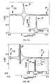
- Fig. 3 shows from above how the structure may also comprise a multitude of gate and drain electrodes.
- Fig. 3a shows an arrangement with two gate electrodes g and two drain electrodes d.
- the gate electrodes are arranged, one on each side of the nanotube 120 and below.
- the drain electrodes d are arranged also one on each side and below of the nanotube 120, and closer to the tip of the tube than the gate electrodes g. This electrode placing enables a greater freedom in control of vibration modes of the nanotube 120.
- Fig. 3b shows an alternative arrangement with one gate electrode g and two drain electrodes d.
- the gate electrode g is arranged directly under the nanotube 120, whilst the two drain electrodes d are arranged, one on each side of the nanotube opposite of each other.
- this arrangement does not form a part of the invention and is not covered by the claims.
- Fig. 3c shows another alternative arrangement with two gate electrodes g and one drain electrode d.
- the gate electrodes are arranged, one on each side of the nanotube 120 and opposite of each other.
- this arrangement does not form a part of the invention and is not covered by the claims.
- Fig. 3d shows an arrangement with four gate electrodes g, and two drain electrodes d.
- the gate electrodes g are arranged two on each side of the nanotube 120 in a quadratic or rectangular fashion in pairs.
- the drain electrodes d are arranged one on each side of the nano-tube opposite of each other.
- Fig. 3e shows an arrangement with two gate electrodes g and two drain electrodes d, where the gate electrodes g are arranged as in fig. 3a and where the drain electrodes d are arranged beyond the nanotube 120, one on each side of the imaginary extension of said tube 120.
- Fig. 3f shows an arrangement with two gate electrodes g and two drain electrodes d where the gate electrodes are arranged asymmetrically with reference to the nanotube 120.
- the tube tip can be electrostatically bent towards the drain electrode by controlling the voltages on the electrodes, thereby inducing an excess charge q on the tube.
- the deflection of the tube tip is measured vertically towards the substrate and is denoted x .
- the tube In the non-contact mode, the tube never reaches the electrode.
- the tube tip-drain contact is a tunnel junction, and decreasing the distance between the tube and the drain electrode reduces the tunnelling resistance R T (x , V) , and allows a tunnelling current I sd to flow over the junction.
- the basic principle of operation is thus to mechanically reduce the barrier width by means of a capacitive coupling, which in turn leads to an electric current in the system.
- fig. 1 shows how an end of a conducting nanotube or nanowhisker of length L is free hanging over a terraced non-conducting substrate on which additional electrodes (gate and drain) are placed underneath the tube.
- the other end of the tube is electrically connected to a source electrode, the distance ⁇ z s controls the tunnelling resistance of the source junction.
- the vertical distance between a straight tube and the gate and drain electrodes is h and the horizontal distance between the tube tip and the electrode is ⁇ z .
- the tube tip can be deflected a distance x in the vertical direction by means of the voltages on the electrodes.
- FIG. 2 shows the corresponding equivalent circuit of the system.
- the parts within the dashed line are the equivalent circuit of the component of fig. 1 , whereas the parts outside said dashed line are external parts. This "box notation" will be used later.
- the tube-source junction is has impedance Z over which a charge q flows, the tube-gate coupling is purely capacitive with capacitance C g (x) and the tube is connected to the drain by a tunnel junction with tunnelling resistance R T (x, V) and capacitance C g (x) .
- a stochastic tunnelling current I sd (x , V) flows between the tube and the drain electrode
- the geometry of the system depends on the electrostatic potentials on the electrodes, and the electrical properties depend in turn of the geometry of the system.
- the equilibrium tube position as a function of gate voltage can be deduced from fig. 4a and the corresponding current voltage characteristics is depicted in fig. 4b .
- the corresponding plots are depicted in fig. 5a and 5b .
- nanorelays are arranged parallelly to each other to increase the possible current through such a structure.
- the tube 120 is a carbon nanotube, a silicon carbide nanotube, a nanowire or a nanowhisker.
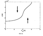
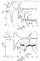
- Fig. 4a shows a stability diagram with and without short range surface forces for a typical contact mode system.
- the large arrows show the direction of the force on each side of the curves, indicating one local equilibrium to be unstable in the region where three equilibria exist.
- the required voltage for pulling the tube to the surface (pull-in voltage) is given by A ( ⁇ 6,73V). This voltage is not significantly affected by surface forces.
- a tube at the surface will not leave the surface until the voltage is lower than the release voltage, B and C in the figure.
- FIG. 4b shows the current voltage characteristics corresponding to the stability plot in fig. 4a with surface forces.
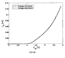
- Fig. 5a shows a stability diagram for the non-contact mode system.
- the arrows show the direction of the force on the tube tip in the two regions. Only one equilibrium position for each voltage is seen for this set of design parameters, and the system characteristics have no hysteresis.
- Fig. 5b shows source-drain current versus source-gate voltage characteristics corresponding to the stability plot in fig. 5a .
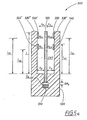
- Fig. 5c shows a top view of another embodiment 500 of the invention.
- This embodiment 500 comprises a nanotube device similar to that shown in fig. 1 and described above, but with the supporting, terraced structure 530 additionally comprising a structure 530" on a third level, said third level 530" being located essentially in parallel with the second level 530', but on a an opposite side of the protruding part of the nanotube 520.
- the embodiment 500 also comprises tunnelling source-tube junction due to the distance ⁇ z s between a source 510 and a nanotube 520.
- the embodiment 500 comprises essentially all of the feature of the device in fig. 1 , and additionally comprises second means 540' for exerting a force upon the nanotube 520 in a second direction defined by its lateral extension, so that when said force exceeds a certain level, the second part of the nanotube will flex in the second direction of its lateral extension, and thereby close or making a tunnel junction in a second electrical circuit.
- Said second direction is, as will be realized from fig. 5 , the direction which is towards the means 540', which are preferably a second gate electrode, the second, protruding part of the nanotube 520 will flex in the second direction of its lateral extension, and thereby close a second electrical circuit.
- This second electrical circuit is suitably defined by the source electrode 510 described in connection with fig. 1 , and a second drain electrode 550' located on the third level 530" of the supporting structure 530.
- the second gate and drain electrodes are located at distances L G2 and L D2 , respectively, from the wall of the terraced structure.
- Short range surface forces influence the operational characteristics if the tube at any time gets closer than a few nanometers from mechanical contact with any part of the structure not including the source electrode.
- the primary net effect of these forces is to increase hysteresis.
- Such a memory element can be designed to be either volatile or non-volatile using, for example, the three-terminal contact mode system or the five terminal structure of patent WO 03078305 .
- volatile refers to an embodiment, where the nanotube is designed to have a mechanical stiffness, such that the mechanical forces due to said stiffness are enough to loosen the nanotube from the drain electrode when V g becomes close to zero.
- the stiffness can be achieved by e.g. a short nanotube or a nanotube with large diameter.
- Non-volatile refers to an embodiment, where it is necessary to provide a current pulse, heating the electrode to loosen said nanotube from the drain electrode. Such a current pulse can be provided by a pulse-generating device connected to the source.
- the high intrinsic mechanical frequency of the device can be used to design components based on a nanoelectromechanical resonances with resonance frequencies reaching the GHz regime.
- the equilibrium positions of the tube which can be deduced from fig. 4a and 5a , are determined by the local minima of the total tube potential.
- the mechanical resonance frequency is determined by the curvature of the total potential near the potential minima (harmonic approximation). Since the total potential can be controlled by the external voltages, both the tube equilibrium position and the mechanical resonance frequency are controllable by electrostatic means.
- the resonance frequency is a function of gate voltage as plotted in fig. 6 for a contact mode device.
- the lowest mechanical resonance frequency denoted by f *, can be varied over several GHz by tuning the gate voltage bias.
- Non-linear effects are important when considering the resonances. These non-linear effects change the location of the main resonance peak and make resonances at half and twice the resonance frequency possible. These resonances are denoted by f * 1/2 and f * 2 respectively.
- fig. 6 shows the lowest resonance frequency of a typical contact mode system as a function of gate voltage. The values are compared to a prediction based on a harmonic approximation to the potential profile.
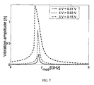
- Fig. 7 shows the vibration amplitude (peak to peak) for the contact mode system as a function of modulation frequency for different values of the modulation amplitude ⁇ V . If the amplitude is small , the line shape is symmetric, whereas for larger amplitudes the shape is asymmetric and the peak position is shifted.
- the resonance is accompanied by a large change in the displacement current.
- the system may impinge on the drain contact for a range of frequencies. Interactions between the tube and the drain electrode cause the tube lose some of its energy and help the tube to get trapped to a stationary state near the surface.
- the potential minimum near the surface corresponds to a high frequency compared to the minima far from the surface, implying that the gate modulation frequency is no longer at resonance, and energy transfer to a tube at the contact position is inefficient.
- the device has changed its state as a result of the modulation and a tunnelling current is feasible.
- the tube will continue to reside at the surface even after the gate modulation is removed.
- the system has a built-in memory, which remembers if a modulation within a certain frequency range has been applied.
- the frequency scan in this case is shown in fig. 8b , where, for a narrow interval near a resonance frequency, the tube ends up near the contact. Only in this narrow region do we get a non-zero tunnelling current. In both cases there are clearly visible resonances at half and the double frequency and, also, the line shape of the main resonance is asymmetric. Both these characteristics are due to deviations from the quadratic potential shape.
- Inset in fig. 8a shows the amplitude of the source junction displacement current as a function of frequency.
- fig. 8b is shown how the tube switches state to a position close to the surface for some frequencies, allowing a non-zero tunnelling current from the tube to the drain, i.e.
- Switches state implies that the tube hits the substrate and sticks for certain frequencies because the amplitude of the oscillation is frequency dependent.
- Inset in fig. 8b depicts both effective displacement current I s,eff , and the drain tunnelling current I sd .
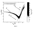
- the contact mode we can predict resonance frequencies for a specific gate voltage using a harmonic approximation to the potential. This prediction is the dashed line in fig. 9 . The prediction is compared to the observed oscillation amplitudes as a function of both gate voltage and modulation frequency. The dark areas correspond to resonances. The observed resonances follow approximately the qualitative behaviour of the harmonic approximation and the frequency for the main resonance can be changed even more than was possible in the non-contact mode system. Also note the f * 1/2 and f * 2 branches that are visible even in this case.
- fig. 9 shows observed resonances in the non-contact mode of operation of the system as a function of modulation frequency and gate voltage bias.
- the harmonic approximation (dashed line) agrees well with the observed resonances in the low bias region and deviates from the predicted value for larger voltages. Note the clearly visible f * 1/2 and f * 2 -branches.
- the current through the system in the non-contact mode is significantly different from the current in the contact mode system.
- the large source-drain voltage allows for a current without mechanical contact and a non-zero tunnelling current is expected for all frequencies.
- the current changes at resonance due to the tube oscillations, and may either increase or decrease depending on bias voltages - if the non-oscillatory position resulted in a large current, oscillations tend to reduce it, and vice versa.
- fig. 10 shows the minimum and maximum tube deflection in the limit cycle
- the insets show the corresponding tunnelling currents.
- the most important conclusion from these figures is that the resonance changes the current, which implies that the resonance is detectable electrically.
- the line shape of the resonances is highly asymmetric, implying that the current changes abruptly on one side of the resonant frequency.
- fig. 10 shows the frequency response in the non-contact mode of operation.
- the main resonance peak is highly asymmetric and both double-frequency and a half-frequency peaks are visible.
- Insets show the average tunnelling current as a function of frequency. The average current increases at the resonance in fig. 10a and decreases in fig. 10b . The sign and magnitude of the current change depend on the shape of the potential.
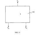
- the box contains a nanomechanical relay device, either in the contact or non-contact mode, and is connected to an external circuit through source, gate, and drain contacts, see fig. 11 .
- a nanomechanical relay device either in the contact or non-contact mode
- source, gate, and drain contacts see fig. 11 .
- a memory element application is a potential application for the relay. Due to inelastic collisions between the tube and drain electrode in the contact mode system very fast writing times are attainable.
- the memory cell may be both volatile, requiring external voltage sources to store its value, or non-volatile, capable of maintaining its state even in the absence of external voltages.
- the box should contain a relay in the contact mode, with sufficient hysteresis as depicted in fig. 4b .
- the conducting state in which the tube end is in close proximity to the drain electrode, is a logical "I", while the non-conducting state is a logical "0".
- the memory cell is volatile, if the lower edge of the hysteresis loop, denoted by B in fig.
- a non-volatile memory element can be reset to a non-conducting state by applying a large voltage pulse V sd , thereby heating up the tube-drain contact. The resulting vigorous electron movements will discharge the tube from the drain electrode.
- the system can be used as a filter by applying the input AS signal to the gate and reading of the output signal at the drain. Modulating the gate voltage with a signal with several frequency components suppresses frequency components with frequencies out of resonance. Since the resonance frequency is tuneable using the gate voltage bias V g0 , the system acts as a tuneable filter.
- the nanoelectromechanical element in this case can be either in the contact or non-contact mode, and the frequency range of the filter can be read off fig. 6 and 9 .
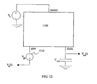
- Fig. 12 shows schematically a filter application of the relay.
- the internal capacitances are functions of time which yields an output voltage which also varies in time with the frequency with which the tube oscillates.
- a gate voltage modulator 1210 is connected between the voltage input V in and the gate, to add an AC voltage.
- the system can be used as detector ( fig. 13 ) which detects signals that are sufficiently close to the resonance frequency.
- the gate of the device 1600 is connected to a gate voltage modulator 1310.
- a gate voltage modulation with an appropriate frequency induces a response.
- the specific features of the response depend on the mode of operation.
- the tube changes its logical state which results in a change in the tunneling resistance, and consequently a DC current at the drain, as shown in fig. 8b .
- the gate modulation is turned off, the tube remains at the surface (unless the gate bias is removed, or even in the absence of gate bias if the design parameters correspond to those of a non-volatile memory element) and the detector has a memory.
- the bandwidth of the detector is a function of both gate bias and signal amplitude and can be tuned.
- the resonance frequency is, as mentioned earlier, a function of gate bias. Thus, both the detector bandwidth and response frequency can be tuned. If the nanoelectromechanical component is in the non-contact mode, the current response at drain may have either sign (cf. Figure 10 ), and the detector has no built-in memory.
- Fig. 13 shows schematically a detector application. If a signal with an appropriate frequency is applied to the gate, the system changes its logical state which results in a source (drain) current.
- the system can be designed with a built-in memory so that the system remembers if a signal has been applied.
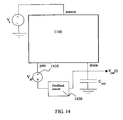
- the capacitance between the tube and the drain electrode is a function of time. Inserting a capacitance between the drain electrode and ground gives a time-dependent voltage, V out (t). With a feedback circuit 1420 connected between the drain and a gate voltage modulator 1410, this time-dependent voltage can be superimposed on the gate voltage bias, which gives a modulation voltage with a frequency corresponding to the vibration frequency of the tube.
- the tube therefore starts to oscillate in resonance.
- the oscillation may be started by applying a step pulse to the gate electrode.
- the oscillation frequency is tunable by the gate bias.
- the nanoelectromechanical component in this example can be either in the contact or non-contact mode.
- fig. 14 shows how an output signal, which has a frequency determined by the resonance frequency, can be fed back via the feedback circuit 1420 to modulate the gate signal. With an appropriate phase shift this signal drives the oscillations.
- the capacitance between the tube and the drain is a function of gate voltage.
- the system can act as a tunable capacitor which in turn can be used in an electrical resonance circuit, see fig. 15 .
- An inductive component 1520 with inductance L is connected between the source and the drain.
- the mechanical oscillation of the tube can be minimized by using a small V sd , or by actively damping tube oscillations using a feedback to the gate with an appropriate phase shift (not depicted in the figure).
- fig. 15 shows a variable capacitor, where the tube-drain capacitance depends on the gate voltage.
- the system is a variable capacitor that can be used to change the resonance frequency of an electric resonance circuit.
- the contact mode system can be used as a pulse generator by applying an AC signal to the gate, with a suitable amplitude and frequency such that, during one cycle, the tube tip contacts the drain electrode for part of the cycle.
- the system By allowing higher mechanical modes of the tube motion, and by applying an AC signal with a suitable frequency to an appropriately placed gate electrode, the system will exhibit coupled mechanical motion, and may be used as a mechanical frequency mixer.
- Additional applications may be constructed by connecting a multitude of individual devices to each other.
- Fig. 16 shows another embodiment of a nanoelectromechanical component according to the present invention.
- the substrate 130 is provided with a cavity 1610 under the nanotube provided with defining surfaces 1630, 1640 and 1650.
- the cavity is preferably having a depth h c and a length L c and a width (not shown) sufficient to house the tube 120, when the tube oscillates with large amplitude as indicated by arrow 1620, thereby enabling greater movement of said nanotube, without the tube 120 making contact with the substrate 130.
- the drain electrode 150 is arranged beyond the tube 120.
Landscapes
- Engineering & Computer Science (AREA)
- Chemical & Material Sciences (AREA)
- Nanotechnology (AREA)
- Materials Engineering (AREA)
- Physics & Mathematics (AREA)
- Theoretical Computer Science (AREA)
- Mathematical Physics (AREA)
- Crystallography & Structural Chemistry (AREA)
- Acoustics & Sound (AREA)
- Thin Film Transistor (AREA)
- Insulated Gate Type Field-Effect Transistor (AREA)
- Micromachines (AREA)
- Semiconductor Integrated Circuits (AREA)
- Semiconductor Memories (AREA)
- Junction Field-Effect Transistors (AREA)
Abstract
Description
- The present invention relates to a nanotechnology component and more particular to a nanoelectromechanical component having means for influencing the flow of a small electrical current through the component.
- Nanotechnology is an expanding research field in which development of nanoelectromechanical systems (NEMS) is included. NEMS is based on an electromechanical coupling in systems with length scales in the nanometer range. The small length scale of these systems allows for high intrinsic mechanical frequencies, and electromechanical resonances in the GHz-regime are possible. These resonances can be used to design high frequency electronic components on the nanometer scale.
- The present invention is a further development of the system presented in patent
WO 03078305 DE 10034315 A1 andWO 0161753 A1 - The present invention is a nanoelectromechanical device as defined in
claim 1. The device comprises a nanotube, preferably a conducting nanotube, suitably a carbon nanotube. - The device further includes a non-conducting supporting structure, made of a non-conducting material such as for example silicon, Si, which supports at least a first portion of the nanotube, with another second portion of the nanotube protruding beyond the supporting structure, and thus being unsupported. The first, supported, portion of the nanotube is connected to an electrode, referred to from now on as the source electrode, by means of a source-tube connection having special properties.
- The source-tube connection is a connection where a source-to-tube distance between the conducting source electrode and the conducting nanotube is in the range where quantum mechanics phenomena, in particular the so called tunnel effect, also called quantum leakage can occur.
- The device according to the invention also provides means for controlling the magnitude of said tunnel effect. Said means preferably comprise two or more gate electrodes, see below.
- Providing such a tunnelling contact at the source-tube junction has the advantages of:
- enabling the control of exact number of electrons in the nanotube;
- a system that can be so devised that every new added amount of charge, which is tunnelled into the nanotube, will correspond to a specific mechanical equilibrium position of the nanotube before the potential is levelled out. This results in a precise mechanism of transportation, usable as a kind of "stepper motor".
- The supporting structure is suitably shaped as a terrace, and thus has a "step-like" structures, with an upper level, and a lower level, where the two levels are interconnected by a wall-like shape of the supporting structure. The difference in height between the two levels of the structure as defined by the height of the wall is referred to by the letter h. It should be noted that the use of the word "level" throughout this description refers to a difference in dimensions which gives the structure a preferably step-like form either in the horizontal or in the vertical orientation of the device.
- On the lower level of the structure, there are arranged two or more additional electrodes, some of which being referred to as gate electrodes and others as the drain electrodes. The gate electrodes are located at a distance LG to the nearest point of the wall, and the corresponding distance for the drain electrodes are denoted as LD, where LG suitably is smaller than LD.
- The total extension of the protruding part of the nanotube is preferably within the interval of 50 to 150 nm, suitably of the order of approximately 100 nm, with the height h being approximately in the order of size of 3 nm.
- When a voltage is applied to the gate electrodes, a resulting capacitive force will act on the nanotube, in the direction towards the gate electrode, which is thus a direction defined by the lateral extension of the nanotube. When the mentioned force acts, the nanotube will deflect towards the gate electrodes, thereby reducing a tube-to-drain distance between the nanotube and the at least two drain electrodes. The amount of deflection is such that the distance between the tube tip and the drain electrodes can be varied from a distance with very high impedance, over a distance where tunnelling phenomena is dominant, to a distance of zero, where the tube tip directly abuts the drain electrode, and impedance is very low.
- By applying voltages of different amplitudes and frequencies the device can be controlled to give different characteristica for a source-drain current flowing from the source electrode through the tube to the drain electrodes, as will be explained below.
- The invention will be described in detail below with reference to the accompanying drawings, in which:
-
Fig. 1 shows a schematic side view of a nanoelectromechanical component according to a preferred embodiment of the present invention. -
Fig. 2 shows an equivalent circuit diagram of the component infig. 1 . -
Fig. 3a-f shows schematically components having different configurations with several gate and drain electrodes. -
Fig. 4a shows a stability diagram showing the positions of zero net forces on the tube of the component infig. 1 for different gate voltages. -
Fig. 4b shows the current as a function of gate voltage corresponding to the stability plot infig. 4a . -
Fig. 5a shows a stability diagram for a non-contact mode system. -
Fig. 5b shows a diagram of the current as a function of source-gate voltage, corresponding to the stability plot infig. 5a . -
Fig. 5c shows a modification of the component infig. 1 . -
Fig. 6 shows a diagram of resonance frequency for a non-contact mode system as a function of gate voltage. -
Fig. 7 shows a diagram of the vibration peak to peak amplitude for a contact mode system as a function of modulation frequency. -
Fig. 8a shows a diagram of maximum and minimum displacements of the tube in a contact mode system as a function of modulation frequency. -
Fig. 8b shows a diagram similar to that infig. 8a , when the tube switches state to a position close to the surface for some frequencies. -
Fig. 9 shows a diagram of observed resonances for a non-contact mode system as a function of modulation frequency and gate voltage bias. -
Fig 10a-b show diagrams of frequency responses in non-contact mode at operation. -
Fig. 11 shows a component according to the invention as a box. -
Fig. 12 shows a schematic illustration of a filter circuit embodiment of the invention. -
Fig. 13 shows a schematic illustration of a detector application of an embodiment of the invention. -
Fig. 14 shows a schematic illustration of a voltage controlled oscillator according to an embodiment of the invention. -
Fig. 15 shows a schematic illustration of a variable capacitor circuit according to an embodiment of the invention. -
Fig. 16 shows a nanoelectromechanical component provided with a cavity enabling greater oscillations of the nanotube. - An illustration of the basic system is depicted in
fig. 1 and the corresponding equivalent circuit is shown infig. 2 . A nanotube or ananowhisker 120, preferably a conducting nanotube, suitably a carbon nanotube, of length L is placed on a terracednon-conducting substrate 130 such that a tip end 160 is free to move and a base end 170 is firmly connected to the terracednon-conducting substrate 130 on the higher part of the terrace - the term higher refers to the figure and does imply a particular spatial orientation. The tube-source contact may be a tunnel junction, corresponding to Δz s>0, or a contact allowing continuous charge transfer if Δz s=0. The impedance of the tube-source contact is denoted by Z and the electrostatic potentials on the source, gate and drain electrodes are denoted V s, V g, V d, respectively. The potential on the tube is V. The direction along the tube axis is denoted z and the tube tip 160 is located at z=L. Two additional electrodes (gate and drain) are positioned beneath the free end of the tube at z g <L and z d = L + Δz respectively. The ratio z g /L = z r gives the relative position of the gate compared to the tube tip, and Δz≥0 distinguishes between two modes of operation. The "contact mode" is defined by Δz = 0 whereas the "non-contact mode" occurs for Δz>>λ, where λ ≈0,5 Å is the tunnelling length. -
Fig. 3 shows from above how the structure may also comprise a multitude of gate and drain electrodes. -
Fig. 3a shows an arrangement with two gate electrodes g and two drain electrodes d. The gate electrodes are arranged, one on each side of thenanotube 120 and below. - The drain electrodes d are arranged also one on each side and below of the
nanotube 120, and closer to the tip of the tube than the gate electrodes g. This electrode placing enables a greater freedom in control of vibration modes of thenanotube 120. -
Fig. 3b shows an alternative arrangement with one gate electrode g and two drain electrodes d. The gate electrode g is arranged directly under thenanotube 120, whilst the two drain electrodes d are arranged, one on each side of the nanotube opposite of each other. However, this arrangement does not form a part of the invention and is not covered by the claims. -
Fig. 3c shows another alternative arrangement with two gate electrodes g and one drain electrode d. The gate electrodes are arranged, one on each side of thenanotube 120 and opposite of each other. However, this arrangement does not form a part of the invention and is not covered by the claims. -
Fig. 3d shows an arrangement with four gate electrodes g, and two drain electrodes d. The gate electrodes g are arranged two on each side of thenanotube 120 in a quadratic or rectangular fashion in pairs. The drain electrodes d are arranged one on each side of the nano-tube opposite of each other. -
Fig. 3e shows an arrangement with two gate electrodes g and two drain electrodes d, where the gate electrodes g are arranged as infig. 3a and where the drain electrodes d are arranged beyond thenanotube 120, one on each side of the imaginary extension of saidtube 120. -
Fig. 3f shows an arrangement with two gate electrodes g and two drain electrodes d where the gate electrodes are arranged asymmetrically with reference to thenanotube 120. - The arrangement of
fig. 3a and 3d-3f allows for greater and different freedom in control of vibration modes of the nanotube. These arrangements make it possible to superimpose movements orthogonally to the elongation of thetube 120 different from the deflection mentioned in connection withfig. 1 . - The tube tip can be electrostatically bent towards the drain electrode by controlling the voltages on the electrodes, thereby inducing an excess charge q on the tube. The deflection of the tube tip is measured vertically towards the substrate and is denoted x. In the contact mode, the tube mechanically contacts the drain electrode when x = h, where h is the vertical distance from the straight tube to the contact. In the non-contact mode, the tube never reaches the electrode. The tube tip-drain contact is a tunnel junction, and decreasing the distance between the tube and the drain electrode reduces the tunnelling resistance R T (x, V), and allows a tunnelling current I sd to flow over the junction. The basic principle of operation is thus to mechanically reduce the barrier width by means of a capacitive coupling, which in turn leads to an electric current in the system.
- In other words,
fig. 1 shows how an end of a conducting nanotube or nanowhisker of length L is free hanging over a terraced non-conducting substrate on which additional electrodes (gate and drain) are placed underneath the tube. The other end of the tube is electrically connected to a source electrode, the distance Δz s controls the tunnelling resistance of the source junction. An ohmic contact is possible if Δz s = 0. The vertical distance between a straight tube and the gate and drain electrodes is h and the horizontal distance between the tube tip and the electrode is Δz. The tube tip can be deflected a distance x in the vertical direction by means of the voltages on the electrodes. A large enough deflection reduces the tunnelling resistance enough to allow for a tunnelling current from the tube tip to the drain electrode.Fig. 2 shows the corresponding equivalent circuit of the system. The parts within the dashed line are the equivalent circuit of the component offig. 1 , whereas the parts outside said dashed line are external parts. This "box notation" will be used later. The tube-source junction is has impedance Z over which a charge q flows, the tube-gate coupling is purely capacitive with capacitance C g (x) and the tube is connected to the drain by a tunnel junction with tunnelling resistance RT(x, V) and capacitance C g (x). A stochastic tunnelling current Isd (x, V) flows between the tube and the drain electrode - There is a strong coupling between the electrical and mechanical degrees of freedom in the system. The geometry of the system depends on the electrostatic potentials on the electrodes, and the electrical properties depend in turn of the geometry of the system. For a typical contact mode system, the equilibrium tube position as a function of gate voltage can be deduced from
fig. 4a and the corresponding current voltage characteristics is depicted infig. 4b . For the non-contact mode system the corresponding plots are depicted infig. 5a and5b . - In one embodiment several nanorelays are arranged parallelly to each other to increase the possible current through such a structure.
- In alternative embodiments the
tube 120 is a carbon nanotube, a silicon carbide nanotube, a nanowire or a nanowhisker. -
Fig. 4a shows a stability diagram with and without short range surface forces for a typical contact mode system. The curve shows the positions of zero net force on the tube (or local equilibria) as functions of gate voltage (at constant V s= 0,01 V) and deflection x (in units of h). The large arrows show the direction of the force on each side of the curves, indicating one local equilibrium to be unstable in the region where three equilibria exist. The required voltage for pulling the tube to the surface (pull-in voltage) is given by A (≈6,73V). This voltage is not significantly affected by surface forces. A tube at the surface will not leave the surface until the voltage is lower than the release voltage, B and C in the figure. Note that A > B, C, which indicates a hysteretic behaviour in the IV g-characteristics, a feature significantly enhanced by surface forces.Fig. 4b shows the current voltage characteristics corresponding to the stability plot infig. 4a with surface forces. -
Fig. 5a shows a stability diagram for the non-contact mode system. The arrows show the direction of the force on the tube tip in the two regions. Only one equilibrium position for each voltage is seen for this set of design parameters, and the system characteristics have no hysteresis.Fig. 5b shows source-drain current versus source-gate voltage characteristics corresponding to the stability plot infig. 5a . -
Fig. 5c shows a top view of anotherembodiment 500 of the invention. Thisembodiment 500 comprises a nanotube device similar to that shown infig. 1 and described above, but with the supporting,terraced structure 530 additionally comprising astructure 530" on a third level, saidthird level 530" being located essentially in parallel with the second level 530', but on a an opposite side of the protruding part of thenanotube 520. - The
embodiment 500 also comprises tunnelling source-tube junction due to the distance Δz s between asource 510 and ananotube 520. - The
embodiment 500 comprises essentially all of the feature of the device infig. 1 , and additionally comprises second means 540' for exerting a force upon thenanotube 520 in a second direction defined by its lateral extension, so that when said force exceeds a certain level, the second part of the nanotube will flex in the second direction of its lateral extension, and thereby close or making a tunnel junction in a second electrical circuit. Said second direction is, as will be realized fromfig. 5 , the direction which is towards the means 540', which are preferably a second gate electrode, the second, protruding part of thenanotube 520 will flex in the second direction of its lateral extension, and thereby close a second electrical circuit. This second electrical circuit is suitably defined by thesource electrode 510 described in connection withfig. 1 , and a second drain electrode 550' located on thethird level 530" of the supportingstructure 530. - The second gate and drain electrodes are located at distances LG2 and LD2, respectively, from the wall of the terraced structure.
- Short range surface forces (forces with a stronger distance dependence than the Coulomb interaction) influence the operational characteristics if the tube at any time gets closer than a few nanometers from mechanical contact with any part of the structure not including the source electrode. The primary net effect of these forces is to increase hysteresis. This makes a memory element a particularly interesting application particularly for the contact mode structure. Such a memory element can be designed to be either volatile or non-volatile using, for example, the three-terminal contact mode system or the five terminal structure of patent
WO 03078305 - The high intrinsic mechanical frequency of the device can be used to design components based on a nanoelectromechanical resonances with resonance frequencies reaching the GHz regime.
- The equilibrium positions of the tube, which can be deduced from
fig. 4a and5a , are determined by the local minima of the total tube potential. The mechanical resonance frequency is determined by the curvature of the total potential near the potential minima (harmonic approximation). Since the total potential can be controlled by the external voltages, both the tube equilibrium position and the mechanical resonance frequency are controllable by electrostatic means. Hence, the resonance frequency is a function of gate voltage as plotted infig. 6 for a contact mode device. The lowest mechanical resonance frequency, denoted by f*, can be varied over several GHz by tuning the gate voltage bias. Non-linear effects are important when considering the resonances. These non-linear effects change the location of the main resonance peak and make resonances at half and twice the resonance frequency possible. These resonances are denoted by f*1/2 and f*2 respectively. - In other words,
fig. 6 shows the lowest resonance frequency of a typical contact mode system as a function of gate voltage. The values are compared to a prediction based on a harmonic approximation to the potential profile. -
Fig. 7 shows the vibration amplitude (peak to peak) for the contact mode system as a function of modulation frequency for different values of the modulation amplitude δV. If the amplitude is small , the line shape is symmetric, whereas for larger amplitudes the shape is asymmetric and the peak position is shifted. - When a high frequency modulation is applied to the gate electrode of a contact mode structure, it may result in two qualitatively different outcomes. In the first case, the system's trajectory in phase space approaches a limit cycle, in which the tube never mechanically contacts the surface, but oscillates with a substantial amplitude. Due to the very high tunnelling resistance for large tube-drain separations, tunnel current through the system is negligible. However, since the geometry of the structure changes in time, so do the geometric capacitances, and also the charge on the tube changes in time with the same frequency. This results in a AC displacement current at the source and drain contacts with a frequency corresponding to the mechanical oscillation frequency. The frequency response of the system in this case is shown in
fig. 8a and the effective value of the displacement current i s,eff, determined assuming sinusoidal charge transfer as i s,eff =
fig. 8b , where, for a narrow interval near a resonance frequency, the tube ends up near the contact. Only in this narrow region do we get a non-zero tunnelling current. In both cases there are clearly visible resonances at half and the double frequency and, also, the line shape of the main resonance is asymmetric. Both these characteristics are due to deviations from the quadratic potential shape. - In other words,
fig. 8 shows the maximum and minimum displacements in a contact mode structure in steady state for gate voltage biases (a) V g0=5 V and (b) V g0=6 V with gate voltage modulation δV=0,1 V with frequency f mod. The largest peak corresponds to the resonance frequency, and the smaller to half and double frequency peaks. Inset infig. 8a shows the amplitude of the source junction displacement current as a function of frequency. Infig. 8b is shown how the tube switches state to a position close to the surface for some frequencies, allowing a non-zero tunnelling current from the tube to the drain, i.e. "switches state" implies that the tube hits the substrate and sticks for certain frequencies because the amplitude of the oscillation is frequency dependent. Inset infig. 8b depicts both effective displacement current I s,eff, and the drain tunnelling current I sd. - As for the contact mode we can predict resonance frequencies for a specific gate voltage using a harmonic approximation to the potential. This prediction is the dashed line in
fig. 9 . The prediction is compared to the observed oscillation amplitudes as a function of both gate voltage and modulation frequency. The dark areas correspond to resonances. The observed resonances follow approximately the qualitative behaviour of the harmonic approximation and the frequency for the main resonance can be changed even more than was possible in the non-contact mode system. Also note the f*1/2 and f*2 branches that are visible even in this case. - In other words,
fig. 9 shows observed resonances in the non-contact mode of operation of the system as a function of modulation frequency and gate voltage bias. The harmonic approximation (dashed line) agrees well with the observed resonances in the low bias region and deviates from the predicted value for larger voltages. Note the clearly visible f*1/2 and f*2-branches. - The current through the system in the non-contact mode is significantly different from the current in the contact mode system. The large source-drain voltage allows for a current without mechanical contact and a non-zero tunnelling current is expected for all frequencies. The current changes at resonance due to the tube oscillations, and may either increase or decrease depending on bias voltages - if the non-oscillatory position resulted in a large current, oscillations tend to reduce it, and vice versa. These two different cases are depicted in
fig. 10 , which shows the minimum and maximum tube deflection in the limit cycle, and the insets show the corresponding tunnelling currents. The most important conclusion from these figures is that the resonance changes the current, which implies that the resonance is detectable electrically. The line shape of the resonances is highly asymmetric, implying that the current changes abruptly on one side of the resonant frequency. - In other words,
fig. 10 shows the frequency response in the non-contact mode of operation. Biasing points are (a) V g0=4,3 V and (b) V g0=4,8 V, amplitude of AC modulation is δ V=0,1 V. The main resonance peak is highly asymmetric and both double-frequency and a half-frequency peaks are visible. Insets show the average tunnelling current as a function of frequency. The average current increases at the resonance infig. 10a and decreases infig. 10b . The sign and magnitude of the current change depend on the shape of the potential. - Dimensions vary with application and expectation of dynamics. In theory typical lengths are 80-100 nanometer, the terrace height h typically 8 nanometer, and the diameter typically 8 nanometer.
- Below are examples of components that can be designed using the system described earlier.
- For simplicity, the examples are described using a box notation. The box contains a nanomechanical relay device, either in the contact or non-contact mode, and is connected to an external circuit through source, gate, and drain contacts, see
fig. 11 . Thus, we consider the system as a box which is connected to external circuits through three or five electrodes. If the relay utilizes the other configuration, e.g. the five-terminal configuration discussed in the patentWO 03078305 - A memory element application is a potential application for the relay. Due to inelastic collisions between the tube and drain electrode in the contact mode system very fast writing times are attainable. The memory cell may be both volatile, requiring external voltage sources to store its value, or non-volatile, capable of maintaining its state even in the absence of external voltages. In the memory application, the box should contain a relay in the contact mode, with sufficient hysteresis as depicted in
fig. 4b . The conducting state, in which the tube end is in close proximity to the drain electrode, is a logical "I", while the non-conducting state is a logical "0". The memory cell is volatile, if the lower edge of the hysteresis loop, denoted by B infig. 4b , is positive. If the hysteresis loop extends to zero gate voltage, the memory element maintains its state even without external voltages, and is non-volatile. A non-volatile memory element can be reset to a non-conducting state by applying a large voltage pulse V sd, thereby heating up the tube-drain contact. The resulting vigorous electron movements will discharge the tube from the drain electrode. - Exploiting the electromechanical resonance the system can be used as a filter by applying the input AS signal to the gate and reading of the output signal at the drain. Modulating the gate voltage with a signal with several frequency components suppresses frequency components with frequencies out of resonance. Since the resonance frequency is tuneable using the gate voltage bias V g0, the system acts as a tuneable filter. The nanoelectromechanical element in this case can be either in the contact or non-contact mode, and the frequency range of the filter can be read off
fig. 6 and9 . -
Fig. 12 shows schematically a filter application of the relay. The internal capacitances are functions of time which yields an output voltage which also varies in time with the frequency with which the tube oscillates. Agate voltage modulator 1210 is connected between the voltage input Vin and the gate, to add an AC voltage. - The system can be used as detector (
fig. 13 ) which detects signals that are sufficiently close to the resonance frequency. The gate of the device 1600 is connected to agate voltage modulator 1310. A gate voltage modulation with an appropriate frequency induces a response. The specific features of the response depend on the mode of operation. For the contact mode system, the tube changes its logical state which results in a change in the tunneling resistance, and consequently a DC current at the drain, as shown infig. 8b . When the gate modulation is turned off, the tube remains at the surface (unless the gate bias is removed, or even in the absence of gate bias if the design parameters correspond to those of a non-volatile memory element) and the detector has a memory. The bandwidth of the detector is a function of both gate bias and signal amplitude and can be tuned. The resonance frequency is, as mentioned earlier, a function of gate bias. Thus, both the detector bandwidth and response frequency can be tuned. If the nanoelectromechanical component is in the non-contact mode, the current response at drain may have either sign (cf.Figure 10 ), and the detector has no built-in memory. -
Fig. 13 shows schematically a detector application. If a signal with an appropriate frequency is applied to the gate, the system changes its logical state which results in a source (drain) current. The system can be designed with a built-in memory so that the system remembers if a signal has been applied. - The capacitance between the tube and the drain electrode is a function of time. Inserting a capacitance between the drain electrode and ground gives a time-dependent voltage, V out (t). With a
feedback circuit 1420 connected between the drain and agate voltage modulator 1410, this time-dependent voltage can be superimposed on the gate voltage bias, which gives a modulation voltage with a frequency corresponding to the vibration frequency of the tube. - This structure is illustrated in
fig. 14 . With the feedback the tube therefore starts to oscillate in resonance. The oscillation may be started by applying a step pulse to the gate electrode. The oscillation frequency is tunable by the gate bias. The nanoelectromechanical component in this example can be either in the contact or non-contact mode. - In other words,
fig. 14 shows how an output signal, which has a frequency determined by the resonance frequency, can be fed back via thefeedback circuit 1420 to modulate the gate signal. With an appropriate phase shift this signal drives the oscillations. - The capacitance between the tube and the drain is a function of gate voltage. Thus, the system can act as a tunable capacitor which in turn can be used in an electrical resonance circuit, see
fig. 15 . Aninductive component 1520 with inductance L is connected between the source and the drain. The mechanical oscillation of the tube can be minimized by using a small V sd, or by actively damping tube oscillations using a feedback to the gate with an appropriate phase shift (not depicted in the figure). - In other words,
fig. 15 shows a variable capacitor, where the tube-drain capacitance depends on the gate voltage. The system is a variable capacitor that can be used to change the resonance frequency of an electric resonance circuit. - The contact mode system can be used as a pulse generator by applying an AC signal to the gate, with a suitable amplitude and frequency such that, during one cycle, the tube tip contacts the drain electrode for part of the cycle.
- By allowing higher mechanical modes of the tube motion, and by applying an AC signal with a suitable frequency to an appropriately placed gate electrode, the system will exhibit coupled mechanical motion, and may be used as a mechanical frequency mixer.
- Additional applications may be constructed by connecting a multitude of individual devices to each other.
-
Fig. 16 shows another embodiment of a nanoelectromechanical component according to the present invention. Thesubstrate 130 is provided with acavity 1610 under the nanotube provided with definingsurfaces tube 120, when the tube oscillates with large amplitude as indicated byarrow 1620, thereby enabling greater movement of said nanotube, without thetube 120 making contact with thesubstrate 130. In this embodiment thedrain electrode 150 is arranged beyond thetube 120.
Claims (21)
- A nanotube device (100), comprising a nanotube (120) with a base end and a tip end and with a longitudinal and a lateral extension, a supporting structure (130) for supporting at least a first part of the nanotube (120) comprising the base end, and a first means comprising two gate electrodes (140, g) for exerting a capacitive force upon the nanotube in a first direction defined by its lateral extension, wherein at least a second part of the nanotube (120) comprising the tip end protrudes beyond the support of said structure (130), so that when said force exceeds a certain level, the second part of the nanotube will flex, and thereby reducing a tube-to-drain distance between the tube (120) and a drain electrode (150), characterized in that a source electrode (110) is arranged having a distance (Δz s>0) to the base end of the nanotube (120) such that tunnelling can be made to occur between the nanotube (120) and said source electrode (110), and wherein said device further comprises two drain electrodes (150, d), and wherein the gate electrodes are arranged, one on each side of the nanotube (120), and below, and wherein the drain electrodes (150, d) are arranged, one on each side and below, relatively to the nanotube (120) and closer to the tip of the tube than the gate electrode.
- A nanotube device according to claim 1, characterized in that the dimensions of said nanotube (120) and a size of a vertical distance (h) between the tube (120) and the supporting structure (130), and a size of a horizontal distance (Δz>0) between a tube (160) and the drain electrode (150) is such that tunneling can be made to occur between the tube (120) and said drain electrode (150).
- A nanotube device according to claims 1 or 2, in which said supporting structure comprises a terraced structure with structures on a first and a second level, with the supported first part of the nanotube being supported by the first level of the structure, and said means for exerting force being located on said second level.
- A nanotube device according to any of claims 1-3, in which a first circuit which impedance is affected by the flexing of the nanotube comprises a first gate electrode being located on said second level of the structure and a first source electrode being located on said first level of the structure.
- A nanotube device according to any of the previous claims, in which the supporting terraced structure additionally comprises a structure on a third level, said third level being located essentially in parallel with said second level, but on an opposite side of the protruding part of the nanotube, which nanotube device comprises second means for exerting a force upon the nanotube in a second direction defined by its lateral extension, so that when said force exceeds a certain level, the second part of the nanotube will flex in the second direction of its lateral extension, and thereby affect the impedance of a second electrical circuit.
- A nanotube device according to claim 5, characterized in that the second means for exerting said force upon the nanotube is an electrical means, the force being created by applying a voltage to the means.
- A nanotube device according to claims 5 or 6, in which said additional supporting structure comprises a terraced structure with structures on a first and a second level, with the supported first part of the nanotube being supported by the first level of the structure, and said means for exerting force being located on said second level.
- A nanotube device according to any of claims 5-7, in which the second means for applying force comprises a second gate electrode, and the second circuit which impedance is affected by the flexing of the nanotube comprises a second drain electrode being located on said third level of the structure.
- A nanotube device (100) according to claim 1, where said device comprises four gate electrodes (g), and two drain electrodes (d), the gate electrodes (g) are arranged two on each side of the nanotube (120) in a quadratic or rectangular fashion in pairs and the drain electrodes (d) are arranged one on each side of the nanotube opposite of each other.
- A nanotube device (100) according to claim 1, where said device comprises two gate electrodes (g) and two drain electrodes (d) where the drain electrodes (d) are arranged one on each side of the nanotube (120) and below and closer to the tip of the tube than the gate electrodes (g) and where the drain electrodes (d) are arranged beyond the nanotube (120), one on each side of the imaginary extension of said tube (120).
- A nanotube device (100) according to claim 1, where said device comprises two gate electrodes (g) and two drain electrodes (d) where the gate electrodes are arranged asymmetrically with reference to the nanotube (120).
- A memory element, characterized in that it comprises the device of claim 1.
- A filter, characterized in that it comprises the device of claim 1, where said device comprises means for applying an input AC signal to the gate of the device, and means for reading the output signal at the drain.
- The filter of claim 13, where said filter comprise means for applying a gate voltage bias for tuning a resonance frequency of said filter.
- A variable bandwidth detector, characterized in that it comprises the device of claim 1, where the gate of the device is connected to a gate voltage modulator (1310).
- An oscillator, characterized in that it comprises the device of claim 1.
- The oscillator of claim 16, where a feedback circuit (1420) is connected between the drain and a gate voltage modulator (1410).
- A variable capacitor, characterized in that it comprises the device of claim 1.
- The capacitor of claim 18, where an inductive component (1520) is connected between the source and the drain.
- A device according to any of the previous claims, where said tube (120) is made of carbon, silicon carbide or metal and/or is a nanowire or a nanowhisker.
- A nanotube device according to claim 1, where said device is provided with a cavity (1610) in the substrate under the nanotube (120) enabling greater movement of said nanotube (120).
Applications Claiming Priority (2)
| Application Number | Priority Date | Filing Date | Title |
|---|---|---|---|
| US57088204P | 2004-05-14 | 2004-05-14 | |
| PCT/SE2005/000691 WO2005112126A1 (en) | 2004-05-14 | 2005-05-16 | Electromechanical nanotube tunneling device comprising source, drain and gate |
Publications (2)
| Publication Number | Publication Date |
|---|---|
| EP1745516A1 EP1745516A1 (en) | 2007-01-24 |
| EP1745516B1 true EP1745516B1 (en) | 2011-11-23 |
Family
ID=35394430
Family Applications (1)
| Application Number | Title | Priority Date | Filing Date |
|---|---|---|---|
| EP05742101A Expired - Lifetime EP1745516B1 (en) | 2004-05-14 | 2005-05-16 | Electromechanical nanotube tunneling device comprising source, drain and gate |
Country Status (5)
| Country | Link |
|---|---|
| US (1) | US20060086994A1 (en) |
| EP (1) | EP1745516B1 (en) |
| JP (1) | JP4995717B2 (en) |
| AT (1) | ATE535021T1 (en) |
| WO (1) | WO2005112126A1 (en) |
Families Citing this family (57)
| Publication number | Priority date | Publication date | Assignee | Title |
|---|---|---|---|---|
| US8749054B2 (en) | 2010-06-24 | 2014-06-10 | L. Pierre de Rochemont | Semiconductor carrier with vertical power FET module |
| US7095645B2 (en) * | 2003-06-02 | 2006-08-22 | Ambient Systems, Inc. | Nanoelectromechanical memory cells and data storage devices |
| US7199498B2 (en) * | 2003-06-02 | 2007-04-03 | Ambient Systems, Inc. | Electrical assemblies using molecular-scale electrically conductive and mechanically flexible beams and methods for application of same |
| US7148579B2 (en) * | 2003-06-02 | 2006-12-12 | Ambient Systems, Inc. | Energy conversion systems utilizing parallel array of automatic switches and generators |
| US20040238907A1 (en) * | 2003-06-02 | 2004-12-02 | Pinkerton Joseph F. | Nanoelectromechanical transistors and switch systems |
| WO2007024204A2 (en) | 2004-07-19 | 2007-03-01 | Ambient Systems, Inc. | Nanometer-scale electrostatic and electromagnetic motors and generators |
| US7405698B2 (en) | 2004-10-01 | 2008-07-29 | De Rochemont L Pierre | Ceramic antenna module and methods of manufacture thereof |
| JP5349956B2 (en) | 2005-04-25 | 2013-11-20 | スモルテック エービー | Controlled growth of nanostructures on substrates and electron-emitting devices based thereon |
| WO2007005642A2 (en) | 2005-06-30 | 2007-01-11 | Derochemont L Pierre | Electrical components and method of manufacture |
| US20070048160A1 (en) * | 2005-07-19 | 2007-03-01 | Pinkerton Joseph F | Heat activated nanometer-scale pump |
| US7612424B1 (en) * | 2005-07-22 | 2009-11-03 | Northwestern University | Nanoelectromechanical bistable cantilever device |
| US7777291B2 (en) | 2005-08-26 | 2010-08-17 | Smoltek Ab | Integrated circuits having interconnects and heat dissipators based on nanostructures |
| JP4599256B2 (en) * | 2005-09-09 | 2010-12-15 | 株式会社東芝 | Magnetic switching element and signal processing apparatus using the same |
| JP4843760B2 (en) * | 2005-12-26 | 2011-12-21 | 株式会社発明屋 | Memory element using carbon nanotube |
| KR100695167B1 (en) * | 2006-01-04 | 2007-03-14 | 삼성전자주식회사 | Nonvolatile Carbon Nanotube Memory Device Using Multi-walled Carbon Nanotube and Its Operation Method |
| US8354294B2 (en) | 2006-01-24 | 2013-01-15 | De Rochemont L Pierre | Liquid chemical deposition apparatus and process and products therefrom |
| EP2033232B1 (en) * | 2006-06-14 | 2018-08-15 | Lumileds Holding B.V. | Lighting device and manufacturing process thereof |
| WO2008124084A2 (en) * | 2007-04-03 | 2008-10-16 | Pinkerton Joseph F | Nanoelectromechanical systems and methods for making the same |
| KR101487346B1 (en) | 2007-09-12 | 2015-01-28 | 스몰텍 에이비 | Connecting and Bonding Adjacent Layers with Nanostructures |
| CN101816079A (en) | 2007-10-15 | 2010-08-25 | 诺基亚公司 | Nanotube device |
| US7932792B2 (en) * | 2008-02-22 | 2011-04-26 | Nokia Corporation | Nanotube device |
| CN102007571B (en) | 2008-02-25 | 2016-01-20 | 斯莫特克有限公司 | Deposition and selective removal of conductive helplayers during nanostructure fabrication |
| US7791433B2 (en) | 2008-02-29 | 2010-09-07 | Nokia Corporation | Apparatus, method, and computer program product providing edgeless carbon nanotube resonator arrays |
| DE102008031820A1 (en) * | 2008-07-04 | 2010-01-14 | Siemens Aktiengesellschaft | Sensor device for measuring an electric field and method for its production |
| DE102008031819A1 (en) * | 2008-07-05 | 2010-01-14 | Forschungszentrum Jülich GmbH | Three or Mehrtorbauelement based on the tunnel effect |
| US7959598B2 (en) | 2008-08-20 | 2011-06-14 | Asante Solutions, Inc. | Infusion pump systems and methods |
| US8922347B1 (en) | 2009-06-17 | 2014-12-30 | L. Pierre de Rochemont | R.F. energy collection circuit for wireless devices |
| US8952858B2 (en) | 2009-06-17 | 2015-02-10 | L. Pierre de Rochemont | Frequency-selective dipole antennas |
| US8044738B2 (en) | 2009-09-10 | 2011-10-25 | Nokia Corporation | Oscillator apparatus |
| US8084336B2 (en) | 2009-09-10 | 2011-12-27 | Nokia Corporation | Oscillator apparatus |
| US8552708B2 (en) | 2010-06-02 | 2013-10-08 | L. Pierre de Rochemont | Monolithic DC/DC power management module with surface FET |
| WO2011159351A2 (en) * | 2010-06-18 | 2011-12-22 | Northwestern University | Electrodes to improve reliability of nanoelectromechanical systems |
| US9023493B2 (en) | 2010-07-13 | 2015-05-05 | L. Pierre de Rochemont | Chemically complex ablative max-phase material and method of manufacture |
| CN103180955B (en) * | 2010-08-23 | 2018-10-16 | L·皮尔·德罗什蒙 | Power Field Effect Transistor with Resonant Transistor Gate |
| CN103415925A (en) | 2010-11-03 | 2013-11-27 | L·皮尔·德罗什蒙 | Semiconductor chip carrier with monolithically integrated quantum dot devices and method of manufacturing the same |
| US9561324B2 (en) | 2013-07-19 | 2017-02-07 | Bigfoot Biomedical, Inc. | Infusion pump system and method |
| GB2518185A (en) | 2013-09-12 | 2015-03-18 | Ibm | Electromechanical switching device wtih 2D layered material surfaces |
| US10275573B2 (en) | 2016-01-13 | 2019-04-30 | Bigfoot Biomedical, Inc. | User interface for diabetes management system |
| HK1256995A1 (en) | 2016-01-14 | 2019-10-11 | Bigfoot Biomedical, Inc. | Occlusion resolution in medication delivery devices, systems, and methods |
| CN108495665B (en) | 2016-01-14 | 2021-04-09 | 比格福特生物医药公司 | Adjust insulin delivery rate |
| US12383166B2 (en) | 2016-05-23 | 2025-08-12 | Insulet Corporation | Insulin delivery system and methods with risk-based set points |
| EP3871708A3 (en) | 2016-05-26 | 2022-01-19 | Insulet Corporation | Wearable drug delivery system comprising a prefilled cartridge |
| WO2018050965A1 (en) * | 2016-09-14 | 2018-03-22 | Aalto University Foundation Sr | An accelerometer device and method for manufacturing the accelerometer device |
| EP3500161A4 (en) | 2016-12-12 | 2020-01-08 | Bigfoot Biomedical, Inc. | ALARMS AND ALERTS FOR MEDICATION DELIVERY DEVICES AND RELATED SYSTEMS AND METHODS |
| US10500334B2 (en) | 2017-01-13 | 2019-12-10 | Bigfoot Biomedical, Inc. | System and method for adjusting insulin delivery |
| WO2018132723A1 (en) | 2017-01-13 | 2018-07-19 | Mazlish Bryan | Insulin delivery methods, systems and devices |
| EP3568859B1 (en) | 2017-01-13 | 2025-12-10 | Insulet Corporation | Insulin delivery methods, systems and devices |
| US10881792B2 (en) | 2017-01-13 | 2021-01-05 | Bigfoot Biomedical, Inc. | System and method for adjusting insulin delivery |
| US10758675B2 (en) | 2017-01-13 | 2020-09-01 | Bigfoot Biomedical, Inc. | System and method for adjusting insulin delivery |
| USD874471S1 (en) | 2017-06-08 | 2020-02-04 | Insulet Corporation | Display screen with a graphical user interface |
| USD928199S1 (en) | 2018-04-02 | 2021-08-17 | Bigfoot Biomedical, Inc. | Medication delivery device with icons |
| USD920343S1 (en) | 2019-01-09 | 2021-05-25 | Bigfoot Biomedical, Inc. | Display screen or portion thereof with graphical user interface associated with insulin delivery |
| USD977502S1 (en) | 2020-06-09 | 2023-02-07 | Insulet Corporation | Display screen with graphical user interface |
| US12491316B2 (en) | 2020-12-18 | 2025-12-09 | Insulet Corporation | Scheduling of medicament bolus deliveries by a medicament delivery device at future dates and times with a computing device |
| US12514980B2 (en) | 2021-06-30 | 2026-01-06 | Insulet Corporation | Adjustment of medicament delivery by a medicament delivery device based on menstrual cycle phase |
| US12521486B2 (en) | 2021-07-16 | 2026-01-13 | Insulet Corporation | Method for modification of insulin delivery during pregnancy in automatic insulin delivery systems |
| CA3275991A1 (en) | 2023-01-06 | 2024-07-11 | Insulet Corporation | Automatically or manually initiated meal bolus delivery with subsequent automatic safety constraint relaxation |
Citations (1)
| Publication number | Priority date | Publication date | Assignee | Title |
|---|---|---|---|---|
| WO2003078305A1 (en) * | 2002-03-20 | 2003-09-25 | Chalmers Intellectual Property Rights Ab | Nanotube relay device |
Family Cites Families (12)
| Publication number | Priority date | Publication date | Assignee | Title |
|---|---|---|---|---|
| US6445006B1 (en) * | 1995-12-20 | 2002-09-03 | Advanced Technology Materials, Inc. | Microelectronic and microelectromechanical devices comprising carbon nanotube components, and methods of making same |
| JP3958330B2 (en) * | 1997-10-30 | 2007-08-15 | キヤノン株式会社 | Carbon nanotube device and manufacturing method thereof |
| DE10006964C2 (en) | 2000-02-16 | 2002-01-31 | Infineon Technologies Ag | Electronic component with a conductive connection between two conductive layers and method for producing an electronic component |
| KR100360476B1 (en) * | 2000-06-27 | 2002-11-08 | 삼성전자 주식회사 | Vertical nano-size transistor using carbon nanotubes and manufacturing method thereof |
| JP4112358B2 (en) * | 2000-07-04 | 2008-07-02 | インフィネオン テクノロジーズ アクチエンゲゼルシャフト | Field effect transistor |
| DE10034315C2 (en) | 2000-07-14 | 2002-11-28 | Infineon Technologies Ag | Analog to digital converter |
| JP4140180B2 (en) * | 2000-08-31 | 2008-08-27 | 富士ゼロックス株式会社 | Transistor |
| US6574130B2 (en) * | 2001-07-25 | 2003-06-03 | Nantero, Inc. | Hybrid circuit having nanotube electromechanical memory |
| US6835613B2 (en) * | 2001-12-06 | 2004-12-28 | University Of South Florida | Method of producing an integrated circuit with a carbon nanotube |
| US7112816B2 (en) * | 2002-04-12 | 2006-09-26 | University Of South Flordia | Carbon nanotube sensor and method of producing the same |
| US20040238907A1 (en) * | 2003-06-02 | 2004-12-02 | Pinkerton Joseph F. | Nanoelectromechanical transistors and switch systems |
| JP2005300490A (en) * | 2004-04-16 | 2005-10-27 | Nippon Telegr & Teleph Corp <Ntt> | Mechanical sensing element and detector |
-
2005
- 2005-05-13 US US11/128,437 patent/US20060086994A1/en not_active Abandoned
- 2005-05-16 EP EP05742101A patent/EP1745516B1/en not_active Expired - Lifetime
- 2005-05-16 WO PCT/SE2005/000691 patent/WO2005112126A1/en not_active Ceased
- 2005-05-16 AT AT05742101T patent/ATE535021T1/en active
- 2005-05-16 JP JP2007513104A patent/JP4995717B2/en not_active Expired - Fee Related
Patent Citations (1)
| Publication number | Priority date | Publication date | Assignee | Title |
|---|---|---|---|---|
| WO2003078305A1 (en) * | 2002-03-20 | 2003-09-25 | Chalmers Intellectual Property Rights Ab | Nanotube relay device |
Non-Patent Citations (1)
| Title |
|---|
| KINARET J.M. ET AL.: "A carbon-nanotube-based nanorelay", APPLIED PHYSICS LETTERS, vol. 82, no. 8, 24 February 2003 (2003-02-24), pages 1287 - 1289 * |
Also Published As
| Publication number | Publication date |
|---|---|
| JP4995717B2 (en) | 2012-08-08 |
| WO2005112126A1 (en) | 2005-11-24 |
| JP2008502125A (en) | 2008-01-24 |
| ATE535021T1 (en) | 2011-12-15 |
| US20060086994A1 (en) | 2006-04-27 |
| EP1745516A1 (en) | 2007-01-24 |
Similar Documents
| Publication | Publication Date | Title |
|---|---|---|
| EP1745516B1 (en) | Electromechanical nanotube tunneling device comprising source, drain and gate | |
| Kinaret et al. | A carbon nanotube based nanorelay | |
| Jonsson et al. | High frequency properties of a CNT-based nanorelay | |
| US20050230710A1 (en) | Nanotube relay device | |
| US9793417B2 (en) | Nanowire nanoelectromechanical field-effect transistors | |
| US8803624B2 (en) | MEMS resonator | |
| US8269578B2 (en) | Resonator having a sideways oscillation compressing one connector while extending another | |
| CN102906846B (en) | Electromechanical switching device and method of operation thereof | |
| Liu et al. | Mechanical response of the isolated cantilever with a floating potential in steady electrostatic field | |
| US9431201B2 (en) | Micromechanical resonant switches and charge pumps | |
| US6798321B2 (en) | Micro electromechanical switches | |
| US6744338B2 (en) | Resonant operation of MEMS switch | |
| US7489211B2 (en) | Electromechanical filter and electrical circuit and electrical equipment employing electromechanical filter | |
| EP1743381B1 (en) | Electromechanical electron transfer devices | |
| US7932792B2 (en) | Nanotube device | |
| Chan et al. | Effects of capacitors, resistors, and residual charges on the static and dynamic performance of electrostatically actuated devices | |
| Mahmoodnia et al. | A novel high tuning ratio MEMS cantilever variable capacitor | |
| JPH0955337A (en) | Variable capacitor | |
| KR20110113847A (en) | Nano Resonator | |
| Yao et al. | Design and analysis of repulsive electrostatic driven MEMS actuators | |
| Ayari et al. | Electromechanical Self-Oscillations of Carbon Field Emitters | |
| Pomarico et al. | Vertical MEMS Resonators for Real‐Time Clock Applications | |
| van Essen | Capacitive MEMS-based sensors: Thermo-mechanical stability and charge trapping | |
| Aravindan et al. | Broadband Piezoelectric Energy Harvesting Using an Array of Mistuned Inverted Cantilever Beams |
Legal Events
| Date | Code | Title | Description |
|---|---|---|---|
| PUAI | Public reference made under article 153(3) epc to a published international application that has entered the european phase |
Free format text: ORIGINAL CODE: 0009012 |
|
| 17P | Request for examination filed |
Effective date: 20061030 |
|
| AK | Designated contracting states |
Kind code of ref document: A1 Designated state(s): AT BE BG CH CY CZ DE DK EE ES FI FR GB GR HU IE IS IT LI LT LU MC NL PL PT RO SE SI SK TR |
|
| DAX | Request for extension of the european patent (deleted) | ||
| 17Q | First examination report despatched |
Effective date: 20080915 |
|
| GRAP | Despatch of communication of intention to grant a patent |
Free format text: ORIGINAL CODE: EPIDOSNIGR1 |
|
| RIC1 | Information provided on ipc code assigned before grant |
Ipc: H01L 29/772 20060101AFI20110526BHEP Ipc: B81B 3/00 20060101ALI20110526BHEP Ipc: H01L 51/30 20060101ALI20110526BHEP Ipc: B82B 1/00 20060101ALI20110526BHEP |
|
| GRAS | Grant fee paid |
Free format text: ORIGINAL CODE: EPIDOSNIGR3 |
|
| GRAA | (expected) grant |
Free format text: ORIGINAL CODE: 0009210 |
|
| AK | Designated contracting states |
Kind code of ref document: B1 Designated state(s): AT BE BG CH CY CZ DE DK EE ES FI FR GB GR HU IE IS IT LI LT LU MC NL PL PT RO SE SI SK TR |
|
| REG | Reference to a national code |
Ref country code: GB Ref legal event code: FG4D |
|
| REG | Reference to a national code |
Ref country code: CH Ref legal event code: EP |
|
| REG | Reference to a national code |
Ref country code: IE Ref legal event code: FG4D |
|
| REG | Reference to a national code |
Ref country code: DE Ref legal event code: R096 Ref document number: 602005031356 Country of ref document: DE Effective date: 20120119 |
|
| REG | Reference to a national code |
Ref country code: NL Ref legal event code: VDEP Effective date: 20111123 |
|
| LTIE | Lt: invalidation of european patent or patent extension |
Effective date: 20111123 |
|
| PG25 | Lapsed in a contracting state [announced via postgrant information from national office to epo] |
Ref country code: IS Free format text: LAPSE BECAUSE OF FAILURE TO SUBMIT A TRANSLATION OF THE DESCRIPTION OR TO PAY THE FEE WITHIN THE PRESCRIBED TIME-LIMIT Effective date: 20120323 Ref country code: LT Free format text: LAPSE BECAUSE OF FAILURE TO SUBMIT A TRANSLATION OF THE DESCRIPTION OR TO PAY THE FEE WITHIN THE PRESCRIBED TIME-LIMIT Effective date: 20111123 |
|
| PG25 | Lapsed in a contracting state [announced via postgrant information from national office to epo] |
Ref country code: GR Free format text: LAPSE BECAUSE OF FAILURE TO SUBMIT A TRANSLATION OF THE DESCRIPTION OR TO PAY THE FEE WITHIN THE PRESCRIBED TIME-LIMIT Effective date: 20120224 Ref country code: SE Free format text: LAPSE BECAUSE OF FAILURE TO SUBMIT A TRANSLATION OF THE DESCRIPTION OR TO PAY THE FEE WITHIN THE PRESCRIBED TIME-LIMIT Effective date: 20111123 Ref country code: SI Free format text: LAPSE BECAUSE OF FAILURE TO SUBMIT A TRANSLATION OF THE DESCRIPTION OR TO PAY THE FEE WITHIN THE PRESCRIBED TIME-LIMIT Effective date: 20111123 Ref country code: BE Free format text: LAPSE BECAUSE OF FAILURE TO SUBMIT A TRANSLATION OF THE DESCRIPTION OR TO PAY THE FEE WITHIN THE PRESCRIBED TIME-LIMIT Effective date: 20111123 Ref country code: PT Free format text: LAPSE BECAUSE OF FAILURE TO SUBMIT A TRANSLATION OF THE DESCRIPTION OR TO PAY THE FEE WITHIN THE PRESCRIBED TIME-LIMIT Effective date: 20120323 Ref country code: NL Free format text: LAPSE BECAUSE OF FAILURE TO SUBMIT A TRANSLATION OF THE DESCRIPTION OR TO PAY THE FEE WITHIN THE PRESCRIBED TIME-LIMIT Effective date: 20111123 |
|
| PG25 | Lapsed in a contracting state [announced via postgrant information from national office to epo] |
Ref country code: CY Free format text: LAPSE BECAUSE OF FAILURE TO SUBMIT A TRANSLATION OF THE DESCRIPTION OR TO PAY THE FEE WITHIN THE PRESCRIBED TIME-LIMIT Effective date: 20111123 |
|
| PG25 | Lapsed in a contracting state [announced via postgrant information from national office to epo] |
Ref country code: DK Free format text: LAPSE BECAUSE OF FAILURE TO SUBMIT A TRANSLATION OF THE DESCRIPTION OR TO PAY THE FEE WITHIN THE PRESCRIBED TIME-LIMIT Effective date: 20111123 Ref country code: EE Free format text: LAPSE BECAUSE OF FAILURE TO SUBMIT A TRANSLATION OF THE DESCRIPTION OR TO PAY THE FEE WITHIN THE PRESCRIBED TIME-LIMIT Effective date: 20111123 Ref country code: BG Free format text: LAPSE BECAUSE OF FAILURE TO SUBMIT A TRANSLATION OF THE DESCRIPTION OR TO PAY THE FEE WITHIN THE PRESCRIBED TIME-LIMIT Effective date: 20120223 Ref country code: SK Free format text: LAPSE BECAUSE OF FAILURE TO SUBMIT A TRANSLATION OF THE DESCRIPTION OR TO PAY THE FEE WITHIN THE PRESCRIBED TIME-LIMIT Effective date: 20111123 Ref country code: CZ Free format text: LAPSE BECAUSE OF FAILURE TO SUBMIT A TRANSLATION OF THE DESCRIPTION OR TO PAY THE FEE WITHIN THE PRESCRIBED TIME-LIMIT Effective date: 20111123 |
|
| PG25 | Lapsed in a contracting state [announced via postgrant information from national office to epo] |
Ref country code: PL Free format text: LAPSE BECAUSE OF FAILURE TO SUBMIT A TRANSLATION OF THE DESCRIPTION OR TO PAY THE FEE WITHIN THE PRESCRIBED TIME-LIMIT Effective date: 20111123 Ref country code: RO Free format text: LAPSE BECAUSE OF FAILURE TO SUBMIT A TRANSLATION OF THE DESCRIPTION OR TO PAY THE FEE WITHIN THE PRESCRIBED TIME-LIMIT Effective date: 20111123 Ref country code: IT Free format text: LAPSE BECAUSE OF FAILURE TO SUBMIT A TRANSLATION OF THE DESCRIPTION OR TO PAY THE FEE WITHIN THE PRESCRIBED TIME-LIMIT Effective date: 20111123 |
|
| REG | Reference to a national code |
Ref country code: AT Ref legal event code: MK05 Ref document number: 535021 Country of ref document: AT Kind code of ref document: T Effective date: 20111123 |
|
| PLBE | No opposition filed within time limit |
Free format text: ORIGINAL CODE: 0009261 |
|
| STAA | Information on the status of an ep patent application or granted ep patent |
Free format text: STATUS: NO OPPOSITION FILED WITHIN TIME LIMIT |
|
| 26N | No opposition filed |
Effective date: 20120824 |
|
| REG | Reference to a national code |
Ref country code: DE Ref legal event code: R097 Ref document number: 602005031356 Country of ref document: DE Effective date: 20120824 |
|
| PG25 | Lapsed in a contracting state [announced via postgrant information from national office to epo] |
Ref country code: MC Free format text: LAPSE BECAUSE OF NON-PAYMENT OF DUE FEES Effective date: 20120531 |
|
| REG | Reference to a national code |
Ref country code: CH Ref legal event code: PL |
|
| GBPC | Gb: european patent ceased through non-payment of renewal fee |
Effective date: 20120516 |
|
| PG25 | Lapsed in a contracting state [announced via postgrant information from national office to epo] |
Ref country code: AT Free format text: LAPSE BECAUSE OF FAILURE TO SUBMIT A TRANSLATION OF THE DESCRIPTION OR TO PAY THE FEE WITHIN THE PRESCRIBED TIME-LIMIT Effective date: 20111123 Ref country code: CH Free format text: LAPSE BECAUSE OF NON-PAYMENT OF DUE FEES Effective date: 20120531 Ref country code: LI Free format text: LAPSE BECAUSE OF NON-PAYMENT OF DUE FEES Effective date: 20120531 |
|
| REG | Reference to a national code |
Ref country code: IE Ref legal event code: MM4A |
|
| REG | Reference to a national code |
Ref country code: FR Ref legal event code: ST Effective date: 20130131 |
|
| REG | Reference to a national code |
Ref country code: DE Ref legal event code: R119 Ref document number: 602005031356 Country of ref document: DE Effective date: 20121201 |
|
| PG25 | Lapsed in a contracting state [announced via postgrant information from national office to epo] |
Ref country code: IE Free format text: LAPSE BECAUSE OF NON-PAYMENT OF DUE FEES Effective date: 20120516 Ref country code: ES Free format text: LAPSE BECAUSE OF FAILURE TO SUBMIT A TRANSLATION OF THE DESCRIPTION OR TO PAY THE FEE WITHIN THE PRESCRIBED TIME-LIMIT Effective date: 20120305 Ref country code: FR Free format text: LAPSE BECAUSE OF NON-PAYMENT OF DUE FEES Effective date: 20120531 Ref country code: GB Free format text: LAPSE BECAUSE OF NON-PAYMENT OF DUE FEES Effective date: 20120516 |
|
| PG25 | Lapsed in a contracting state [announced via postgrant information from national office to epo] |
Ref country code: DE Free format text: LAPSE BECAUSE OF NON-PAYMENT OF DUE FEES Effective date: 20121201 Ref country code: FI Free format text: LAPSE BECAUSE OF FAILURE TO SUBMIT A TRANSLATION OF THE DESCRIPTION OR TO PAY THE FEE WITHIN THE PRESCRIBED TIME-LIMIT Effective date: 20111123 |
|
| PG25 | Lapsed in a contracting state [announced via postgrant information from national office to epo] |
Ref country code: TR Free format text: LAPSE BECAUSE OF FAILURE TO SUBMIT A TRANSLATION OF THE DESCRIPTION OR TO PAY THE FEE WITHIN THE PRESCRIBED TIME-LIMIT Effective date: 20111123 |
|
| PG25 | Lapsed in a contracting state [announced via postgrant information from national office to epo] |
Ref country code: LU Free format text: LAPSE BECAUSE OF NON-PAYMENT OF DUE FEES Effective date: 20120516 |
|
| PG25 | Lapsed in a contracting state [announced via postgrant information from national office to epo] |
Ref country code: HU Free format text: LAPSE BECAUSE OF FAILURE TO SUBMIT A TRANSLATION OF THE DESCRIPTION OR TO PAY THE FEE WITHIN THE PRESCRIBED TIME-LIMIT Effective date: 20050516 |