EP1744442A2 - Method and apparatus to limit maximum current in a switch of a switching power supply - Google Patents
Method and apparatus to limit maximum current in a switch of a switching power supply Download PDFInfo
- Publication number
- EP1744442A2 EP1744442A2 EP06253518A EP06253518A EP1744442A2 EP 1744442 A2 EP1744442 A2 EP 1744442A2 EP 06253518 A EP06253518 A EP 06253518A EP 06253518 A EP06253518 A EP 06253518A EP 1744442 A2 EP1744442 A2 EP 1744442A2
- Authority
- EP
- European Patent Office
- Prior art keywords
- switch
- current
- controller
- coupled
- power supply
- Prior art date
- Legal status (The legal status is an assumption and is not a legal conclusion. Google has not performed a legal analysis and makes no representation as to the accuracy of the status listed.)
- Granted
Links
- 238000000034 method Methods 0.000 title claims abstract description 19
- 238000012546 transfer Methods 0.000 claims abstract description 22
- 230000004044 response Effects 0.000 claims abstract description 13
- 230000001105 regulatory effect Effects 0.000 claims description 12
- 230000033228 biological regulation Effects 0.000 claims description 6
- 238000004804 winding Methods 0.000 description 9
- 230000009471 action Effects 0.000 description 6
- 238000001514 detection method Methods 0.000 description 6
- 238000010586 diagram Methods 0.000 description 6
- 230000007423 decrease Effects 0.000 description 5
- 238000012545 processing Methods 0.000 description 5
- 238000005259 measurement Methods 0.000 description 4
- GZPBVLUEICLBOA-UHFFFAOYSA-N 4-(dimethylamino)-3,5-dimethylphenol Chemical compound CN(C)C1=C(C)C=C(O)C=C1C GZPBVLUEICLBOA-UHFFFAOYSA-N 0.000 description 3
- 230000001934 delay Effects 0.000 description 3
- 239000003990 capacitor Substances 0.000 description 2
- 230000005669 field effect Effects 0.000 description 2
- 229910044991 metal oxide Inorganic materials 0.000 description 2
- 150000004706 metal oxides Chemical class 0.000 description 2
- 230000003071 parasitic effect Effects 0.000 description 2
- 239000004065 semiconductor Substances 0.000 description 2
- 230000003213 activating effect Effects 0.000 description 1
- 230000009118 appropriate response Effects 0.000 description 1
- 238000007796 conventional method Methods 0.000 description 1
- 239000013256 coordination polymer Substances 0.000 description 1
- 230000003111 delayed effect Effects 0.000 description 1
- 238000007599 discharging Methods 0.000 description 1
- 238000005516 engineering process Methods 0.000 description 1
- 230000001939 inductive effect Effects 0.000 description 1
- 238000012986 modification Methods 0.000 description 1
- 230000004048 modification Effects 0.000 description 1
- 230000001681 protective effect Effects 0.000 description 1
- 230000009467 reduction Effects 0.000 description 1
- 230000001052 transient effect Effects 0.000 description 1
Images



Classifications
-
- H—ELECTRICITY
- H02—GENERATION; CONVERSION OR DISTRIBUTION OF ELECTRIC POWER
- H02M—APPARATUS FOR CONVERSION BETWEEN AC AND AC, BETWEEN AC AND DC, OR BETWEEN DC AND DC, AND FOR USE WITH MAINS OR SIMILAR POWER SUPPLY SYSTEMS; CONVERSION OF DC OR AC INPUT POWER INTO SURGE OUTPUT POWER; CONTROL OR REGULATION THEREOF
- H02M3/00—Conversion of DC power input into DC power output
- H02M3/22—Conversion of DC power input into DC power output with intermediate conversion into AC
- H02M3/24—Conversion of DC power input into DC power output with intermediate conversion into AC by static converters
- H02M3/28—Conversion of DC power input into DC power output with intermediate conversion into AC by static converters using discharge tubes with control electrode or semiconductor devices with control electrode to produce the intermediate AC
- H02M3/325—Conversion of DC power input into DC power output with intermediate conversion into AC by static converters using discharge tubes with control electrode or semiconductor devices with control electrode to produce the intermediate AC using devices of a triode or a transistor type requiring continuous application of a control signal
- H02M3/335—Conversion of DC power input into DC power output with intermediate conversion into AC by static converters using discharge tubes with control electrode or semiconductor devices with control electrode to produce the intermediate AC using devices of a triode or a transistor type requiring continuous application of a control signal using semiconductor devices only
- H02M3/33507—Conversion of DC power input into DC power output with intermediate conversion into AC by static converters using discharge tubes with control electrode or semiconductor devices with control electrode to produce the intermediate AC using devices of a triode or a transistor type requiring continuous application of a control signal using semiconductor devices only with automatic control of the output voltage or current, e.g. flyback converters
-
- H—ELECTRICITY
- H02—GENERATION; CONVERSION OR DISTRIBUTION OF ELECTRIC POWER
- H02M—APPARATUS FOR CONVERSION BETWEEN AC AND AC, BETWEEN AC AND DC, OR BETWEEN DC AND DC, AND FOR USE WITH MAINS OR SIMILAR POWER SUPPLY SYSTEMS; CONVERSION OF DC OR AC INPUT POWER INTO SURGE OUTPUT POWER; CONTROL OR REGULATION THEREOF
- H02M1/00—Details of apparatus for conversion
- H02M1/32—Means for protecting converters other than automatic disconnection
-
- H—ELECTRICITY
- H02—GENERATION; CONVERSION OR DISTRIBUTION OF ELECTRIC POWER
- H02M—APPARATUS FOR CONVERSION BETWEEN AC AND AC, BETWEEN AC AND DC, OR BETWEEN DC AND DC, AND FOR USE WITH MAINS OR SIMILAR POWER SUPPLY SYSTEMS; CONVERSION OF DC OR AC INPUT POWER INTO SURGE OUTPUT POWER; CONTROL OR REGULATION THEREOF
- H02M1/00—Details of apparatus for conversion
- H02M1/0003—Details of control, feedback or regulation circuits
- H02M1/0009—Devices or circuits for detecting current in a converter
-
- H—ELECTRICITY
- H02—GENERATION; CONVERSION OR DISTRIBUTION OF ELECTRIC POWER
- H02M—APPARATUS FOR CONVERSION BETWEEN AC AND AC, BETWEEN AC AND DC, OR BETWEEN DC AND DC, AND FOR USE WITH MAINS OR SIMILAR POWER SUPPLY SYSTEMS; CONVERSION OF DC OR AC INPUT POWER INTO SURGE OUTPUT POWER; CONTROL OR REGULATION THEREOF
- H02M1/00—Details of apparatus for conversion
- H02M1/0003—Details of control, feedback or regulation circuits
- H02M1/0038—Circuits or arrangements for suppressing, e.g. by masking incorrect turn-on or turn-off signals, e.g. due to current spikes in current mode control
-
- Y—GENERAL TAGGING OF NEW TECHNOLOGICAL DEVELOPMENTS; GENERAL TAGGING OF CROSS-SECTIONAL TECHNOLOGIES SPANNING OVER SEVERAL SECTIONS OF THE IPC; TECHNICAL SUBJECTS COVERED BY FORMER USPC CROSS-REFERENCE ART COLLECTIONS [XRACs] AND DIGESTS
- Y10—TECHNICAL SUBJECTS COVERED BY FORMER USPC
- Y10S—TECHNICAL SUBJECTS COVERED BY FORMER USPC CROSS-REFERENCE ART COLLECTIONS [XRACs] AND DIGESTS
- Y10S323/00—Electricity: power supply or regulation systems
- Y10S323/908—Inrush current limiters
Definitions
- the present invention relates generally to electronic circuits, and more specifically, the invention relates to switched mode power supplies.
- Switches in switching power supplies can sustain damage from excess voltage, excess current, or particular combinations of voltage and current.
- the instantaneous voltage and current must remain within a boundary defined as the safe operating area to prevent damage to the switch. Therefore, controllers for switching power supplies usually measure voltage and current for the purpose of protecting the switch as well as for regulating an output.
- a switching regulator according to claim 1.
- Preferable features of this aspect are set out in claims 2 to 8.
- a method for regulating a transfer of energy according to claim 9 Preferable features of the second aspect are set out in claims 10 to 14.
- a power supply according to claim 15 Preferable features of the third aspect are set out in claims 16 to 20.
- Figure 1 is a functional block diagram of one embodiment of a switching power supply that may limit peak current in a power switch in accordance with the teaching of the present invention.
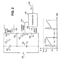
- Figure 2 is a section of a functional block diagram of one embodiment of a switching power supply that shows the contribution of parasitic capacitance to the current in the power switch.
- Figure 3 shows voltage and current waveforms from one embodiment of a switching power supply that may limit peak current in a power switch in accordance with the teaching of the present invention.
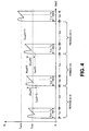
- Figure 4 illustrates important parameters of current waveforms from a switching power supply that limits peak current in a power switch in accordance with the teaching of the present invention.
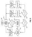
- Figure 5 is a flow diagram that illustrates a method to limit peak current in a power switch in accordance with the teaching of the present invention.
- Figure 6 is a functional block diagram of an integrated circuit that limits peak current in an included power switch in accordance with the teachings of the present invention.
- Embodiments of a power supply regulator that may be utilized in a power supply are disclosed.
- numerous specific details are set forth in order to provide a thorough understanding of the present invention. It will be apparent, however, to one having ordinary skill in the art that the specific detail need not be employed to practice the present invention. Well-known methods related to the implementation have not been described in detail in order to avoid obscuring the present invention.
- Figure 1 shows generally a functional block diagram of a power supply for an embodiment of a power supply that limits peak switch current in accordance with the teachings of the present invention.
- the topology of the example power supply illustrated in Figure 1 is a flyback regulator. It is appreciated that there are many topologies and configurations of switching regulators, and that the flyback topology shown in Figure 1 is provided for explanation purposes and that other types of topologies may also be employed in accordance with the teachings of the present invention.
- FIG. 1 shows that although various embodiments of the present invention are described herein in the context of a power supply for explanation purposes, it is appreciated that the teachings of the present invention may also apply to other technologies such as for example other applications that may involve inductive load switching or the like.
- an energy transfer element T1 125 is coupled between an unregulated input voltage V IN 105 and a load 165 at an output of the power supply.
- a switch S 1 120 is coupled to the primary winding 175 at an input of energy transfer element 125 to regulate the transfer of energy from the unregulated input voltage V IN 105 to the load 165 at the output of the power supply.
- a controller 145 is coupled to generate a drive signal 156 that is coupled to be received by the switch S 1 120 to control switching of switch S 1 120.
- Controller 145 also includes a current sensor coupled to receive current sense 140 that senses a current I D 115 in switch S 1 120.
- the current sensor in controller 145 for one embodiment includes first and second comparators coupled to compare the current I D 115 with first and second current limits, respectively. The second current limit is greater than the first current limit.
- the controller 145 will cause drive signal 156 to open the switch S 1 120 for the remainder of the current switching cycle of the switch until the beginning of the next switching cycle of the switch if the current I D 115 is greater than the first or second current limits.
- the controller 145 also includes a frequency adjuster coupled to the second comparator. The frequency adjuster will adjust an oscillating frequency of an oscillator included in the controller to delay the next switching cycle of the switch if the current I D 115 is greater than the second current limit in accordance with the teachings of the present invention.
- the energy transfer element T1 125 is illustrated as a transformer with two windings.
- a primary winding 175 has N P turns with an inductance L P .
- a secondary winding has N S turns.
- the transformer can have more than two windings, with additional windings to provide power to additional loads, or to provide bias voltages, or to sense the voltage at a load, or the like.
- a clamp circuit 110 is coupled to the primary winding 175 of the energy transfer element T1 125 to control the maximum voltage on the switch S1 120.
- switch S 1 120 is switched on and off in response to a drive signal 156 generated by a controller circuit 145.
- switch S 1 120 is a transistor such as for example a power metal oxide semiconductor field effect transistor (MOSFET).
- controller 145 includes integrated circuits and discrete electrical components. The operation of switch S 1 120 produces pulsating current in the rectifier D1 130 that is filtered by capacitor C1 135 to produce a substantially constant output voltage V O or a substantially constant output current I O at the load 165.
- the output quantity to be regulated is U O 150, that in general could be an output voltage V O , an output current I O , or a combination of the two.
- a feedback circuit 160 is coupled to the output quantity U O 150 to produce a feedback signal U FB 155 that is an input to the controller 145.
- Another input to the controller 145 is the current sense signal 140 that senses a current I D 115 in switch S 1 120. Any of the many known ways to measure a switched current, such as for example a current transformer, or for example the voltage across a discrete resistor, or for example the voltage across a transistor when the transistor is conducting, may be used to measure current I D 115.
- the controller may use current sense signal 140 to regulate the output U O 150 or to prevent damage to the switch S1 120.
- Figure 1 also illustrates an example waveform for current I D 115 through switch S 1 120 under ideal conditions.
- the switch S 1 120 conducts for a time t ON in response to a pulse in the drive signal 156 from controller 145.
- Switch S1 120 is open for an off time t OFF in response to the drive signal 156 from controller 145.
- the current increases linearly with time from an initial current I VAL to a final current I PEAK in response to the input voltage V IN 105 that is imposed across the inductance L P of the primary winding 175 of the transformer T1 125 when the switch S 1 120 is conducting.
- controller 145 operates switch S1 120 to substantially regulate the output U O 150 to its desired value. For one embodiment, controller 145 increases conduction time t ON of the switch S1 120 when output U O 150 is less than its desired value. For one embodiment, controller 145 decreases conduction time t ON of the switch S 1 120 when output U O 150 is greater than its desired value.
- controller 145 adjusts the operation of the switch S1 120 with the drive signal 156 to prevent operation outside its safe operating area. For one embodiment, controller 145 reduces conduction time t ON of the switch S1 120 when current I D 115 exceeds a current limit I LIMIT . For one embodiment, controller 145 increases off time t OFF when current I D 115 exceeds a current limit I LIMIT .
- Figure 2 shows the contribution of stray capacitance to the current I D 215 that is measured in switch S 1 220. Charging and discharging of stray capacitance represented by capacitors C P 210 and C DS 230 coupled to switch S 1 at node 235 augments the current I D 215 for a short time after switch S1 220 turns on.
- Figure 2 also shows the voltage V P 270 on inductance L P of primary winding 275 of transformer T1 225.
- voltage V P is positive with magnitude V IN during the on time t ON .
- voltage V P is negative with magnitude V OR during the off time t OFF .
- the abrupt reversal of polarity in voltage V P adds a leading edge current to the initial current I VAL of switch S1 220.
- the waveforms in Figure 2 show a peak leading edge current I LEPEAK that is greater than the ideal initial current I VAL .
- the peak leading edge current I LEPEAK is also greater than final current I PEAK .
- the stray capacitance that is present in every practical circuit can produce a high leading edge current that can interfere with the ability of a controller to regulate an output or to protect a switch.
- a controller that responds to the magnitude of switch current I D 215 to regulate an output or to protect a switch would also respond to the leading edge current that is not significantly related to the regulation of the output or to the safe operation of the switch.
- controllers typically mask the measurement of current in the switch until after a leading edge blanking time t LEB .
- the relationship of leading edge blanking time t LEB to the conduction time t ON is shown in Figure 3.
- the leading edge blanking time t LEB is long enough to guarantee that the contribution of current from stray capacitance is negligible before the current I D becomes visible to the controller.
- Figure 3 also shows current limit delay time t d that is the difference between the time I D reaches I LIMIT after t LEB and the time when the switch stops conducting.
- Current limit delay time t d is always present because practical circuits cannot respond instantaneously.
- Finite current limit delay time t d has a consequence of peak current I PEAK at the end of conduction time t ON being greater than current limit I LIMIT .
- FIG. 4 illustrates an undesirable situation that can occur in a switching power supply with a typical controller when the output is less than its regulated value.
- an overload at the output causes the switch current I D to exceed I LIMIT in every switching period.
- the overload has also caused the output voltage V O to drop far below its regulated value.
- the controller measures switch current I D at the end of leading edge blanking time t LEB , and the switch opens after current limit delay time t d .
- the detection of I D greater than I LIMIT cannot reduce the on time t ON below the sum of t LEB plus t d .
- Figure 4 shows that in any switching period (n), the current that appears as switch current I D during the on time (exclusive of any current from parasitic capacitance) increases by amount ⁇ I ON during the on time to reach I PEAK , and then decreases from I PEAK by an amount ⁇ I OFF during the off time.
- the changes in current are related to the input and output voltages by Equation 1 and Equation 2.
- Equation 1 shows that the leading edge blanking time t LEB and the current limit delay time t d impose a minimum value on ⁇ I ON . Therefore, the usual method of control will allow ⁇ I ON to be greater than ⁇ I OFF during an overload of the output.
- ⁇ I ON is greater than ⁇ I OFF , the current and voltage can go outside the safe operating area of the switch after only a few consecutive switching periods. Fault detection circuits that respond only after many switching periods are unable to protect the switch from failure. The controller must respond within a small number of switching periods to keep the operation of the switch within its safe operating area.
- FIG. 5 is a flow diagram that describes one example method to keep the operation of the switch within its safe operating area in accordance with the teachings of the present invention.
- the illustrated method measures whether or not I D has exceeded a second current limit I LIMIT2 , which is greater than a first current limit I LIMIT , to determine whether or not an alternative control action is to be performed to help prevent the peak switch current I PEAK from becoming excessive.
- I D is greater than I LIMIT2 at any time during a switching period except during the leading edge blanking time t LEB after the start of the period.
- the alternative control action opens the switch and delays the start of the next switching period.
- the alternative control action reduces the frequency of an oscillator to effectively lengthen the switching period to delay the start of the next switching period.
- detection of current I D greater than I LIMIT2 sets a flag that is reset by a switching period that is not lengthened. If there is a detection of I D greater than I LIMIT2 while the flag is set (two consecutive periods with a detection of I D greater than I LIMIT2 ), then there is an extra lengthening of the period such that the second lengthened switching period is longer than the first lengthened switching period.
- the alternative control actions provide uninterrupted regulation of the output in contrast to other protective actions that cause the output to lose regulation, such as for example latching the power supply off or entering an auto-restart mode of operation.
- processing in Figure begins at block 505 and then proceeds to block 510 where a switching period begins.
- processing waits until the on time t ON has been on at least the leading edge blanking time t LEB .
- the current I D through the switch is measured.
- Block 525 in conjunction with block 530 show that while the current I D is not greater than I LIMIT and while the switch is enabled, the current I D through the switch is measured in block 520. If the current I D remains not greater than I LIMIT until the end of the switching period is indicated in block 535, processing then returns to block 510 where the next switching period then begins.
- both blocks 545 and 555 show that the switch is opened for the remainder of the current switching cycle and will not be closed again until the beginning of the next switching cycle.
- the switch is opened asynchronously or substantially immediately such that the current switching cycle is not allowed to be completed normally.
- block 550 shows that it is next determined whether the current I D reaches the greater second current limit I LIMIT2 . If not, then at block 545 the switch is opened for the remainder of the current switching cycle until the end of the switching period or until the next switching cycle, as indicated at block 540. Processing then returns to block 510 to begin the next switching period or cycle.
- FIG. 6 shows one example of a method according to the teachings of the present invention implemented in an example integrated circuit 600.
- integrated circuit 600 includes power metal oxide semiconductor field effect transistor (MOSFET) switch 628 that is coupled to a drain terminal 602 and a source terminal 646.
- a terminal 648 receives a feedback signal U FB .
- integrated circuit 600 may optionally include one or more other terminals that receive signals and perform functions that are not described in this example.
- a modulator 626 interprets the feedback signal U FB from terminal 648 to determine whether an enable signal 662 should be high or low.
- An oscillator 640 provides a clock signal 644 and a maximum on-time signal D MAX 664.
- the oscillator 640 includes a FREQ ADJ terminal coupled to an output of latch 638.
- the frequency of oscillator 640 changes from a higher frequency to a lower frequency in response to the output of latch 638.
- Switch 628 responds to a drive signal 656 generated at the output of a latch 634, which receives signals from AND gate 632 and OR gate 666.
- Switch 628 is on if both clock 644 and enable 662 are high while both D MAX 644 and OVER CURRENT 650 are low. Switch 628 is off if either D MAX 664 or OVER CURRENT 650 is high.
- a current sensor or current limiting circuit is realized with comparators 604 and 605 as shown.
- one of the terminals of comparator 604 is coupled to sense the current I D through switch 628 and compare it to the first current limit I LIMIT , which is coupled to the other terminal of comparator 604.
- AND gate 606 is coupled to receive the output of comparator 604 and t LEB DELAY 622. Whenever I D exceeds I LIMIT after the blanking time delay t LEB , the output of AND gate 606 goes high to reset latch 634 through OR gate 666 to turn off switch 628.
- comparator 605 is shown to compare I D with I LIMIT2 . As shown, if I D exceeds I LIMIT2 at any time in the switching period after t LEB , then the output of comparator 605 goes high, causing the output 660 of AND gate 607 to go high setting latch 638.
- a frequency adjuster is realized in accordance with the teachings of the present invention with latch 638 and the FREQ ADJ input of oscillator 640.
- oscillator 640 when latch 638 is set, oscillator 640 changes from a higher frequency to a lower frequency, which effectively delays the start of the next switching period in accordance with the teachings of the present invention.
- oscillator 640 is configured such that setting latch 638 and thereby activating the FREQ ADJ input of oscillator 640 causes the next pulse of the drive signal to be skipped, which effectively causes the frequency of oscillator 640 to be reduced in accordance with the teachings of the present invention.
- latch 638 is reset at the start of the next switching period by the CLOCK signal 644.
Landscapes
- Engineering & Computer Science (AREA)
- Power Engineering (AREA)
- Dc-Dc Converters (AREA)
Abstract
Description
- The present invention relates generally to electronic circuits, and more specifically, the invention relates to switched mode power supplies.
- Switches in switching power supplies can sustain damage from excess voltage, excess current, or particular combinations of voltage and current. The instantaneous voltage and current must remain within a boundary defined as the safe operating area to prevent damage to the switch. Therefore, controllers for switching power supplies usually measure voltage and current for the purpose of protecting the switch as well as for regulating an output.
- Conflicting requirements and limitations of real devices often make it impossible or impractical for controllers to measure the quantities necessary to protect the switch under all conditions. Whereas maximum voltage on the switch can usually be deduced from a simple measurement of the dc input voltage, measurement of the current in the switch is usually much more difficult.
- Controllers typically must mask the measurement of switch current at certain times in the switching period to avoid false indications of excess current. Moreover, there will always be some delay between the detection of excess current and an appropriate response. Thus, conventional methods may be unable to protect the switch from damage under certain conditions of transient loading or faults.
According to a first aspect of the invention, there is provided a switching regulator according toclaim 1. Preferable features of this aspect are set out in claims 2 to 8.
According to a second aspect of the invention, there is provided a method for regulating a transfer of energy according to claim 9. Preferable features of the second aspect are set out in claims 10 to 14.
According to a third aspect of the invention, there is provided a power supply according to claim 15. Preferable features of the third aspect are set out in claims 16 to 20. - The present invention detailed illustrated by way of example and not limitation in the accompanying Figures.
- Figure 1 is a functional block diagram of one embodiment of a switching power supply that may limit peak current in a power switch in accordance with the teaching of the present invention.
- Figure 2 is a section of a functional block diagram of one embodiment of a switching power supply that shows the contribution of parasitic capacitance to the current in the power switch.
- Figure 3 shows voltage and current waveforms from one embodiment of a switching power supply that may limit peak current in a power switch in accordance with the teaching of the present invention.
- Figure 4 illustrates important parameters of current waveforms from a switching power supply that limits peak current in a power switch in accordance with the teaching of the present invention.
- Figure 5 is a flow diagram that illustrates a method to limit peak current in a power switch in accordance with the teaching of the present invention.
- Figure 6 is a functional block diagram of an integrated circuit that limits peak current in an included power switch in accordance with the teachings of the present invention.
- Embodiments of a power supply regulator that may be utilized in a power supply are disclosed. In the following description, numerous specific details are set forth in order to provide a thorough understanding of the present invention. It will be apparent, however, to one having ordinary skill in the art that the specific detail need not be employed to practice the present invention. Well-known methods related to the implementation have not been described in detail in order to avoid obscuring the present invention.
- Reference throughout this specification to "one embodiment" or "an embodiment" means that a particular feature, structure, or characteristic described in connection with the embodiment is included in at least one embodiment of the present invention. Thus, the appearances of the phrases "for one embodiment" or "in an embodiment" in various places throughout this specification are not necessarily all referring to the same embodiment. Furthermore, the particular features, structures, or characteristics may be combined in any suitable manner in one or more embodiments.
- During start-up or overload when the power supply has a low output voltage, traditional techniques that respond to excessive current in the power switch cannot prevent the current from going higher in each switching period while allowing the power supply to operate because leading edge blanking time and current limit delay time impose a minimum on time of the switch. Moreover, the controller responds to the low output voltage with a minimum off time for the current to decrease. Techniques are disclosed that use multiple current limit values to determine the need to engage an alternative control mode that extends the off time of the switch to allow the current to decrease to a safe value. Therefore, techniques are disclosed to prevent excess current in a switch of a switching power supply. For one embodiment, switch current is measured against multiple current limit values to recognize a condition of uncontrolled increasing current. Recognition of uncontrolled increasing current engages an alternative control action that delays the start of subsequent switching periods.
- To illustrate, Figure 1 shows generally a functional block diagram of a power supply for an embodiment of a power supply that limits peak switch current in accordance with the teachings of the present invention. The topology of the example power supply illustrated in Figure 1 is a flyback regulator. It is appreciated that there are many topologies and configurations of switching regulators, and that the flyback topology shown in Figure 1 is provided for explanation purposes and that other types of topologies may also be employed in accordance with the teachings of the present invention. Furthermore, it is noted that although various embodiments of the present invention are described herein in the context of a power supply for explanation purposes, it is appreciated that the teachings of the present invention may also apply to other technologies such as for example other applications that may involve inductive load switching or the like.
- As illustrated in the power supply example of Figure 1, an energy
transfer element T1 125 is coupled between an unregulatedinput voltage V IN 105 and aload 165 at an output of the power supply. Aswitch S 1 120 is coupled to theprimary winding 175 at an input ofenergy transfer element 125 to regulate the transfer of energy from the unregulatedinput voltage V IN 105 to theload 165 at the output of the power supply. Acontroller 145 is coupled to generate adrive signal 156 that is coupled to be received by theswitch S 1 120 to control switching ofswitch S 1 120.Controller 145 also includes a current sensor coupled to receivecurrent sense 140 that senses acurrent I D 115 inswitch S 1 120. - As will be discussed below, the current sensor in
controller 145 for one embodiment includes first and second comparators coupled to compare thecurrent I D 115 with first and second current limits, respectively. The second current limit is greater than the first current limit. For one embodiment, thecontroller 145 will causedrive signal 156 to open theswitch S 1 120 for the remainder of the current switching cycle of the switch until the beginning of the next switching cycle of the switch if thecurrent I D 115 is greater than the first or second current limits. For one embodiment, thecontroller 145 also includes a frequency adjuster coupled to the second comparator. The frequency adjuster will adjust an oscillating frequency of an oscillator included in the controller to delay the next switching cycle of the switch if thecurrent I D 115 is greater than the second current limit in accordance with the teachings of the present invention. - In the example of Figure 1, the energy
transfer element T1 125 is illustrated as a transformer with two windings. Aprimary winding 175 has NP turns with an inductance LP. A secondary winding has NS turns. In general, the transformer can have more than two windings, with additional windings to provide power to additional loads, or to provide bias voltages, or to sense the voltage at a load, or the like. - A
clamp circuit 110 is coupled to theprimary winding 175 of the energytransfer element T1 125 to control the maximum voltage on theswitch S1 120. As mentioned,switch S 1 120 is switched on and off in response to adrive signal 156 generated by acontroller circuit 145. For one embodiment,switch S 1 120 is a transistor such as for example a power metal oxide semiconductor field effect transistor (MOSFET). For one embodiment,controller 145 includes integrated circuits and discrete electrical components. The operation ofswitch S 1 120 produces pulsating current in therectifier D1 130 that is filtered bycapacitor C1 135 to produce a substantially constant output voltage VO or a substantially constant output current IO at theload 165. - The output quantity to be regulated is
U O 150, that in general could be an output voltage VO, an output current IO, or a combination of the two. Afeedback circuit 160 is coupled to theoutput quantity U O 150 to produce afeedback signal U FB 155 that is an input to thecontroller 145. Another input to thecontroller 145 is thecurrent sense signal 140 that senses acurrent I D 115 inswitch S 1 120. Any of the many known ways to measure a switched current, such as for example a current transformer, or for example the voltage across a discrete resistor, or for example the voltage across a transistor when the transistor is conducting, may be used to measurecurrent I D 115. The controller may usecurrent sense signal 140 to regulate theoutput U O 150 or to prevent damage to theswitch S1 120. - Figure 1 also illustrates an example waveform for current ID 115 through
switch S 1 120 under ideal conditions. Theswitch S 1 120 conducts for a time tON in response to a pulse in thedrive signal 156 fromcontroller 145.Switch S1 120 is open for an off time tOFF in response to thedrive signal 156 fromcontroller 145. During the time of conduction tON, the current increases linearly with time from an initial current IVAL to a final current IPEAK in response to theinput voltage V IN 105 that is imposed across the inductance LP of the primary winding 175 of thetransformer T1 125 when theswitch S 1 120 is conducting. - For one embodiment,
controller 145 operatesswitch S1 120 to substantially regulate theoutput U O 150 to its desired value. For one embodiment,controller 145 increases conduction time tON of theswitch S1 120 whenoutput U O 150 is less than its desired value. For one embodiment,controller 145 decreases conduction time tON of theswitch S 1 120 whenoutput U O 150 is greater than its desired value. - For one embodiment,
controller 145 adjusts the operation of theswitch S1 120 with thedrive signal 156 to prevent operation outside its safe operating area. For one embodiment,controller 145 reduces conduction time tON of theswitch S1 120 whencurrent I D 115 exceeds a current limit ILIMIT. For one embodiment,controller 145 increases off time tOFF whencurrent I D 115 exceeds a current limit ILIMIT. - Figure 2 shows the contribution of stray capacitance to the current ID 215 that is measured in
switch S 1 220. Charging and discharging of stray capacitance represented by capacitors CP 210 andC DS 230 coupled to switchS 1 atnode 235 augments thecurrent I D 215 for a short time afterswitch S1 220 turns on. Figure 2 also shows thevoltage V P 270 on inductance LP of primary winding 275 oftransformer T1 225. For one embodiment, voltage VP is positive with magnitude VIN during the on time tON. For one embodiment, voltage VP is negative with magnitude VOR during the off time tOFF. The abrupt reversal of polarity in voltage VP adds a leading edge current to the initial current IVAL ofswitch S1 220. The waveforms in Figure 2 show a peak leading edge current ILEPEAK that is greater than the ideal initial current IVAL. For one embodiment, the peak leading edge current ILEPEAK is also greater than final current IPEAK. The stray capacitance that is present in every practical circuit can produce a high leading edge current that can interfere with the ability of a controller to regulate an output or to protect a switch. A controller that responds to the magnitude of switch current ID 215 to regulate an output or to protect a switch would also respond to the leading edge current that is not significantly related to the regulation of the output or to the safe operation of the switch. To avoid interference from leading edge current, controllers typically mask the measurement of current in the switch until after a leading edge blanking time tLEB. The relationship of leading edge blanking time tLEB to the conduction time tON is shown in Figure 3. - The leading edge blanking time tLEB is long enough to guarantee that the contribution of current from stray capacitance is negligible before the current ID becomes visible to the controller. Figure 3 also shows current limit delay time td that is the difference between the time ID reaches ILIMIT after tLEB and the time when the switch stops conducting. Current limit delay time td is always present because practical circuits cannot respond instantaneously. Finite current limit delay time td has a consequence of peak current IPEAK at the end of conduction time tON being greater than current limit ILIMIT.
- Leading edge blanking time tLEB and current limit delay td can make it impossible for typical controllers to limit the switch current ID. Figure 4 illustrates an undesirable situation that can occur in a switching power supply with a typical controller when the output is less than its regulated value. In Figure 4, an overload at the output causes the switch current ID to exceed ILIMIT in every switching period. The overload has also caused the output voltage VO to drop far below its regulated value. The controller measures switch current ID at the end of leading edge blanking time tLEB, and the switch opens after current limit delay time td. The detection of ID greater than ILIMIT cannot reduce the on time tON below the sum of tLEB plus td.
- Figure 4 shows that in any switching period (n), the current that appears as switch current ID during the on time (exclusive of any current from parasitic capacitance) increases by amount ΔION during the on time to reach IPEAK, and then decreases from IPEAK by an amount ΔIOFF during the off time. The changes in current are related to the input and output voltages by
Equation 1 and Equation 2.

It is clear from Figure 4 that when ΔION > ΔIOFF for every consecutive pulse or switching period, the peak current of the next switching period (n+1) will be greater than the peak current in the present switching period (n). An overload condition that reduces the output voltage VO substantially below its regulated value will cause the control circuit to make the off time tOFF as small as possible. Equation 2 shows that reduction of VO with constant or reduced tOFF will reduce ΔIOFF.Equation 1 shows that the leading edge blanking time tLEB and the current limit delay time td impose a minimum value on ΔION. Therefore, the usual method of control will allow ΔION to be greater than ΔIOFF during an overload of the output. When ΔION is greater than ΔIOFF, the current and voltage can go outside the safe operating area of the switch after only a few consecutive switching periods. Fault detection circuits that respond only after many switching periods are unable to protect the switch from failure. The controller must respond within a small number of switching periods to keep the operation of the switch within its safe operating area. - Figure 5 is a flow diagram that describes one example method to keep the operation of the switch within its safe operating area in accordance with the teachings of the present invention. With reference to the example waveforms of Figure 4, the illustrated method measures whether or not ID has exceeded a second current limit ILIMIT2, which is greater than a first current limit ILIMIT, to determine whether or not an alternative control action is to be performed to help prevent the peak switch current IPEAK from becoming excessive. In the example described in Figure 5, there is an alternative control action if ID is greater than ILIMIT2 at any time during a switching period except during the leading edge blanking time tLEB after the start of the period. The alternative control action opens the switch and delays the start of the next switching period. For one embodiment, the alternative control action reduces the frequency of an oscillator to effectively lengthen the switching period to delay the start of the next switching period. In one embodiment, detection of current ID greater than ILIMIT2 sets a flag that is reset by a switching period that is not lengthened. If there is a detection of ID greater than ILIMIT2 while the flag is set (two consecutive periods with a detection of ID greater than ILIMIT2), then there is an extra lengthening of the period such that the second lengthened switching period is longer than the first lengthened switching period. The alternative control actions provide uninterrupted regulation of the output in contrast to other protective actions that cause the output to lose regulation, such as for example latching the power supply off or entering an auto-restart mode of operation.
- In particular, processing in Figure begins at
block 505 and then proceeds to block 510 where a switching period begins. Atblock 515, processing waits until the on time tON has been on at least the leading edge blanking time tLEB. Atblock 520, the current ID through the switch is measured.Block 525 in conjunction withblock 530 show that while the current ID is not greater than ILIMIT and while the switch is enabled, the current ID through the switch is measured inblock 520. If the current ID remains not greater than ILIMIT until the end of the switching period is indicated inblock 535, processing then returns to block 510 where the next switching period then begins. - However, if the current ID reaches a value greater than the current limit ILIMIT, then both
blocks block 545 the switch is opened for the remainder of the current switching cycle until the end of the switching period or until the next switching cycle, as indicated atblock 540. Processing then returns to block 510 to begin the next switching period or cycle. If it is determined atblock 550 that current ID reaches the second current limit ILIMIT2, then the switch is opened atblock 555 and the beginning of the next switching period is delayed atblock 560 in accordance with the teachings of the present invention. After the delay ofblock 560, processing then returns to block 510 to begin the next switching period. By waiting the extra time provided during the extra delay inblock 560, the current ID is given a chance to decrease sufficiently to help limit the maximum current ID through the switch and help prevent the current and/or voltage at switch from going outside the safe operating area in accordance with the teachings of the present invention. - Figure 6 shows one example of a method according to the teachings of the present invention implemented in an example
integrated circuit 600. In the illustrated example, integratedcircuit 600 includes power metal oxide semiconductor field effect transistor (MOSFET)switch 628 that is coupled to adrain terminal 602 and asource terminal 646. A terminal 648 receives a feedback signal UFB. For one embodiment, integratedcircuit 600 may optionally include one or more other terminals that receive signals and perform functions that are not described in this example. - In the example of Figure 6, a
modulator 626 interprets the feedback signal UFB from terminal 648 to determine whether an enablesignal 662 should be high or low. Anoscillator 640 provides aclock signal 644 and a maximum on-time signal D MAX 664. In the illustrated example, theoscillator 640 includes a FREQ ADJ terminal coupled to an output oflatch 638. For one embodiment, the frequency ofoscillator 640 changes from a higher frequency to a lower frequency in response to the output oflatch 638.Switch 628 responds to adrive signal 656 generated at the output of alatch 634, which receives signals from ANDgate 632 andOR gate 666.Switch 628 is on if bothclock 644 and enable 662 are high while bothD MAX 644 and OVERCURRENT 650 are low.Switch 628 is off if eitherD MAX 664 or OVERCURRENT 650 is high. - In the example of Figure 6, a current sensor or current limiting circuit according the teachings of the present invention is realized with
comparators comparator 604 is coupled to sense the current ID throughswitch 628 and compare it to the first current limit ILIMIT, which is coupled to the other terminal ofcomparator 604. ANDgate 606 is coupled to receive the output ofcomparator 604 and tLEB DELAY 622. Whenever ID exceeds ILIMIT after the blanking time delay tLEB, the output of ANDgate 606 goes high to resetlatch 634 through ORgate 666 to turn offswitch 628. In the illustrated example,comparator 605 is shown to compare ID with ILIMIT2. As shown, if ID exceeds ILIMIT2 at any time in the switching period after tLEB, then the output ofcomparator 605 goes high, causing theoutput 660 of ANDgate 607 to gohigh setting latch 638. - In the example shown in Figure 6, a frequency adjuster is realized in accordance with the teachings of the present invention with
latch 638 and the FREQ ADJ input ofoscillator 640. For one embodiment, whenlatch 638 is set,oscillator 640 changes from a higher frequency to a lower frequency, which effectively delays the start of the next switching period in accordance with the teachings of the present invention. For one embodiment,oscillator 640 is configured such that settinglatch 638 and thereby activating the FREQ ADJ input ofoscillator 640 causes the next pulse of the drive signal to be skipped, which effectively causes the frequency ofoscillator 640 to be reduced in accordance with the teachings of the present invention. In the illustrated example,latch 638 is reset at the start of the next switching period by theCLOCK signal 644. - In the foregoing detailed description, the methods and apparatuses of the present invention have been described with reference to a specific exemplary embodiment thereof. It will, however, be evident that various modifications and changes may be made thereto without departing from the broader spirit and scope of the present invention. The present specification and figures are accordingly to be regarded as illustrative rather than restrictive.
Claims (20)
- A switching regulator circuit, comprising:a switch (120, 220) to be coupled to an energy transfer element (125, 225);a controller (145, 245) coupled to the switch to control switching of the switch;a current sensor included in the controller and including first and second comparators (604, 605) coupled to compare a current in the switch with first and second current limits, respectively, the controller to open the switch for a remainder of a current switching cycle of the switch until a next switching cycle of the switch in response to the first or second comparators; anda frequency adjuster included in the controller and coupled to the second comparator, the frequency adjuster to adjust an oscillating frequency of an oscillator (640) included in the controller in response to the second comparator.
- A switching regulator according to claim 1, wherein the frequency adjuster is to reduce the oscillating frequency of the oscillator to delay the next switching cycle of the switch in response to the second comparator.
- A switching regulator according to claim 1, wherein the frequency adjuster is to reduce the oscillating frequency of the oscillator to skip the next switching cycle of the switch in response to the second comparator.
- A switching regulator according to any one of the preceding claims, wherein the controller is included in an integrated circuit.
- A switching regulator according to claim 4, wherein the switch is included in the integrated circuit.
- A switching regulator according to any one of the preceding claims, wherein the second current limit is greater than the first current limit.
- A switching regulator according to any one of the preceding claims, further comprising a leading edge blanking circuit included in the controller and coupled to the current sensor.
- A switching regulator according to any one of the preceding claims, wherein the frequency adjuster is to adjust the oscillating frequency of the oscillator to provide uninterrupted regulation at an output coupled to the energy transfer element.
- A method for regulating a transfer of energy, comprising:switching a switch (120, 220) coupled to an energy transfer element (125, 225) to regulate a transfer of energy through the energy transfer element;opening the switch for a remainder of a current switching cycle of the switch until a next switching cycle of the switch if a current in the switch is greater than a first or second current limit; anddelaying the next switching cycle of the switch if the current in the switch is greater than the second current limit.
- A method for regulating the transfer of energy according to claim 9, wherein delaying the next switching cycle of the switch comprises adjusting a frequency of an oscillator (640) if the current in the switch is greater than the second current limit.
- A method for regulating the transfer of energy according to claim 9, wherein delaying the next switching cycle of the switch comprises skipping the next switching cycle of the switch if the current in the switch is greater than the second current limit.
- A method for regulating the transfer of energy according to any one of claims 9 to 11, wherein the second current limit is greater than the first current limit.
- A method for regulating the transfer of energy according to any one of claims 9 to 12, further comprising ignoring the current through the switch during a leading edge blanking time of each switching cycle of the switch.
- A method for regulating the transfer of energy according to claim 9, wherein the delaying of the next switching cycle comprises maintaining uninterrupted regulation of an output coupled to the energy transfer element.
- A power supply, comprising:an energy transfer element (125, 225) coupled between an input and an output of the power supply;a switch (120, 220) coupled to the input of the energy transfer element to regulate a transfer of energy from the input of the power supply to the output of the power supply;a controller (145, 245) coupled to the switch to control switching of the switch;a current sensor included in the controller and including first and second comparators (604, 605) coupled to compare a current in the switch with first and second current limits, respectively, the controller to open the switch for a remainder of a current switching cycle of the switch until a next switching cycle of the switch in response to the first or second comparators; anda frequency adjuster included in the controller and coupled to the second comparator, the frequency adjuster to adjust an oscillating frequency of an oscillator (640) included in the controller in response to the second comparator.
- A power supply according to claim 15, further comprising a feedback circuit coupled between the output of the power supply and the controller to provide a feedback signal from the output of the power supply to the controller.
- A power supply according to claim 15 or 16, further comprising an integrated circuit including the controller.
- A power supply according to claim 17, wherein the integrated circuit further comprises the switch.
- A power supply according to any one of claims 15 to 18, wherein the second current limit is greater than the first current limit.
- A power supply according to any one of claims 15 to 19, wherein the frequency adjuster is to adjust the oscillating frequency of the oscillator to provide uninterrupted regulation at the output of the power supply.
Applications Claiming Priority (1)
| Application Number | Priority Date | Filing Date | Title |
|---|---|---|---|
| US11/177,096 US7613019B2 (en) | 2005-07-08 | 2005-07-08 | Method and apparatus to limit maximum switch current in a switch of a switching power supply |
Related Child Applications (1)
| Application Number | Title | Priority Date | Filing Date |
|---|---|---|---|
| EP11153613 Division-Into | 2011-02-08 |
Publications (3)
| Publication Number | Publication Date |
|---|---|
| EP1744442A2 true EP1744442A2 (en) | 2007-01-17 |
| EP1744442A3 EP1744442A3 (en) | 2008-04-30 |
| EP1744442B1 EP1744442B1 (en) | 2012-09-05 |
Family
ID=37459342
Family Applications (1)
| Application Number | Title | Priority Date | Filing Date |
|---|---|---|---|
| EP06253518A Not-in-force EP1744442B1 (en) | 2005-07-08 | 2006-07-05 | Method and apparatus to limit maximum current in a switch of a switching power supply |
Country Status (4)
| Country | Link |
|---|---|
| US (1) | US7613019B2 (en) |
| EP (1) | EP1744442B1 (en) |
| JP (1) | JP4928180B2 (en) |
| CN (2) | CN1913312B (en) |
Cited By (2)
| Publication number | Priority date | Publication date | Assignee | Title |
|---|---|---|---|---|
| EP1978626A3 (en) * | 2007-04-06 | 2016-06-15 | Power Integrations, Inc. | Method and apparatus for sensing input and output voltages from a single terminal of a d.c. converter controller |
| WO2018052516A1 (en) * | 2016-09-15 | 2018-03-22 | Peregrine Semiconductor Corporation | Current protected integrated transformer driver for isolating a dc-dc convertor |
Families Citing this family (30)
| Publication number | Priority date | Publication date | Assignee | Title |
|---|---|---|---|---|
| US7593245B2 (en) | 2005-07-08 | 2009-09-22 | Power Integrations, Inc. | Method and apparatus to limit maximum switch current in a switching power supply |
| US7576528B2 (en) | 2006-10-04 | 2009-08-18 | Power Integrations, Inc. | Control circuit responsive to an impedance |
| US7518885B2 (en) * | 2006-10-04 | 2009-04-14 | Power Integrations, Inc. | Method and apparatus for a control circuit with multiple operation modes |
| US7502236B2 (en) | 2006-10-04 | 2009-03-10 | Power Integrations, Inc. | Power supply controller responsive to a feedforward signal |
| US7764520B2 (en) * | 2007-04-06 | 2010-07-27 | Power Integrations, Inc. | Method and apparatus for on/off control of a power converter |
| US8035254B2 (en) | 2007-04-06 | 2011-10-11 | Power Integrations, Inc. | Method and apparatus for integrated cable drop compensation of a power converter |
| KR101284827B1 (en) | 2007-05-21 | 2013-07-10 | 페어차일드코리아반도체 주식회사 | A switch contoller, a control method of the switch, and a converter using the switch controller |
| JP2010022097A (en) * | 2008-07-09 | 2010-01-28 | Panasonic Corp | Switching control circuit, semiconductor device, and switching power source apparatus |
| US7903435B2 (en) * | 2008-08-05 | 2011-03-08 | System General Corp. | Switching controller having switching frequency hopping for power converter |
| US7986149B2 (en) * | 2008-08-19 | 2011-07-26 | Infineon Technologies Austria Ag | System and method for adaptive load fault detection |
| CN101656465B (en) * | 2008-08-22 | 2012-04-04 | 通嘉科技股份有限公司 | Control circuit, power converter and control method |
| US8933677B2 (en) * | 2009-04-08 | 2015-01-13 | Intel Corporation | Voltage regulator controller frequency varied by load current |
| US8098506B2 (en) * | 2009-06-02 | 2012-01-17 | Power Integrations, Inc. | Single-stage power supply with power factor correction and constant current output |
| US9184653B2 (en) * | 2012-06-20 | 2015-11-10 | Fairchild Korea Semiconductor Ltd | Short sensing circuit, short sensing method and power supply device comprising the short sensing circuit |
| US9628065B2 (en) * | 2012-10-05 | 2017-04-18 | Fisher-Rosemount Systems, Inc. | Safety instrumented process control apparatus and methods |
| US9401657B2 (en) * | 2013-03-13 | 2016-07-26 | Power Integrations, Inc. | Input voltage sensor responsive to load conditions |
| EP2963793A1 (en) * | 2014-07-04 | 2016-01-06 | Nxp B.V. | A SMPC, controller therefor, power supply and a method of controlling a SMPC |
| CN105652074B (en) | 2014-12-03 | 2018-08-10 | 万国半导体(开曼)股份有限公司 | Voltage detecting circuit and the method for detecting voltage change |
| CN105763030B (en) * | 2014-12-17 | 2018-07-13 | 万国半导体(开曼)股份有限公司 | In the circuit and method that electric pressure converter startup stage inhibits electric current excessive |
| CN105763061B (en) | 2014-12-17 | 2018-05-29 | 万国半导体(开曼)股份有限公司 | Flyback converter output current counting circuit and computational methods |
| JP6525732B2 (en) * | 2015-05-28 | 2019-06-05 | 三菱電機株式会社 | Power conversion circuit and switching power supply using the same |
| TWI535167B (en) * | 2015-06-22 | 2016-05-21 | 晶宏半導體股份有限公司 | Boost converter for reducing injection current and driving method thereof |
| CN105071641B (en) * | 2015-08-14 | 2017-10-31 | 东南大学 | A kind of control method for improving Switching Power Supply dynamic response |
| US9602088B1 (en) * | 2015-09-11 | 2017-03-21 | Texas Instruments Incorporated | Ultra-low power comparator with sampling control loop adjusting frequency and/or sample aperture window |
| JP6698303B2 (en) * | 2015-09-29 | 2020-05-27 | ローム株式会社 | Semiconductor device |
| US10027231B2 (en) * | 2016-06-10 | 2018-07-17 | Semiconductor Components Industries, Llc | Auto-tuning current limiter |
| US10756614B2 (en) * | 2018-06-11 | 2020-08-25 | Qualcomm Incorporated | Lossless average input and output current sensing in a switched-mode power supply |
| US12021439B2 (en) | 2019-05-24 | 2024-06-25 | Power Integrations, Inc. | Switching delay for communication |
| WO2021216716A2 (en) * | 2020-04-21 | 2021-10-28 | Go Electric Inc. | Adaptable precharge |
| WO2023277922A1 (en) | 2021-07-02 | 2023-01-05 | Power Integrations, Inc. | Adaptive ramp time modulation |
Citations (2)
| Publication number | Priority date | Publication date | Assignee | Title |
|---|---|---|---|---|
| US4791544A (en) | 1984-09-21 | 1988-12-13 | Veeco Instruments | Regulating control for single-ended switching power supply |
| US4928200A (en) | 1987-04-02 | 1990-05-22 | Cherry Semiconductor Corporation | Overcurrent protection for switching mode power converter |
Family Cites Families (30)
| Publication number | Priority date | Publication date | Assignee | Title |
|---|---|---|---|---|
| US4616301A (en) * | 1984-04-30 | 1986-10-07 | Boschert Inc. | Regulator control system |
| US4716510A (en) * | 1986-05-05 | 1987-12-29 | Motorola, Inc. | Automatic restart circuit for a switching power supply |
| US5088016A (en) * | 1990-09-17 | 1992-02-11 | Vlt Corporation | Voltage-compliant dc-dc converter module |
| US5229707A (en) * | 1991-05-14 | 1993-07-20 | National Semiconductor Corporation | Apparatus and method for eliminating false current limit triggering in a grounded source-emitter power switching circuit |
| US5164659A (en) * | 1991-08-29 | 1992-11-17 | Warren Schultz | Switching circuit |
| US5335162A (en) * | 1993-01-15 | 1994-08-02 | Toko America, Inc. | Primary side controller for regulated power converters |
| KR100320672B1 (en) * | 1995-12-30 | 2002-05-13 | 김덕중 | Switching control integrated circuit |
| EP0871328B1 (en) * | 1997-04-09 | 2003-08-13 | STMicroelectronics S.r.l. | Control of the output power of a dc-dc converter upon varying the switching frequency |
| JPH11215690A (en) * | 1998-01-29 | 1999-08-06 | Canon Inc | Overcurrent protection device |
| JP3415759B2 (en) * | 1998-02-17 | 2003-06-09 | 富士通アクセス株式会社 | Overcurrent protection circuit for switching power supply |
| EP0991170B1 (en) * | 1998-09-28 | 2003-11-26 | STMicroelectronics S.r.l. | Integrated protection from the effects of a short circuit of the output of a flyback converter |
| US6151226A (en) * | 1999-05-05 | 2000-11-21 | Marconi Communications, Inc. | Four quadrant power conversion topology |
| US6804129B2 (en) * | 1999-07-22 | 2004-10-12 | 02 Micro International Limited | High-efficiency adaptive DC/AC converter |
| JP2001145338A (en) * | 1999-11-18 | 2001-05-25 | Cosel Co Ltd | Switching power supply |
| US6525514B1 (en) * | 2000-08-08 | 2003-02-25 | Power Integrations, Inc. | Method and apparatus for reducing audio noise in a switching regulator |
| DE10040413B4 (en) * | 2000-08-18 | 2006-11-09 | Infineon Technologies Ag | Circuit arrangement for generating a switching signal for a current-controlled switching power supply |
| DE60025635T2 (en) * | 2000-09-28 | 2006-11-02 | Stmicroelectronics S.A. | Limiting the continuous mode of a power converter |
| DE60029800T2 (en) * | 2000-12-05 | 2007-02-22 | Infineon Technologies Ag | Frequency limiting and overload detection in a voltage regulator |
| US6788555B2 (en) * | 2002-09-26 | 2004-09-07 | Koninklijke Philips Electronics N.V. | Regulation of bi-directional flyback converter |
| JP3657256B2 (en) * | 2002-12-25 | 2005-06-08 | 松下電器産業株式会社 | Switching power supply |
| US6788038B1 (en) * | 2003-01-29 | 2004-09-07 | National Semiconductor Corporation | Apparatus and method for deactivating an on-switch of a circuit for a variable time interval |
| JP3748262B2 (en) * | 2003-06-24 | 2006-02-22 | ローム株式会社 | Switching type DC-DC converter |
| JP3948448B2 (en) * | 2003-10-09 | 2007-07-25 | 松下電器産業株式会社 | Switching power supply |
| JP3957682B2 (en) * | 2003-12-19 | 2007-08-15 | シャープ株式会社 | Switching power supply device and electronic device using the same |
| US7116563B2 (en) * | 2004-05-19 | 2006-10-03 | Semtech Corporation | Dual mode over-current protection for switching mode power converter |
| JP3973652B2 (en) * | 2004-05-24 | 2007-09-12 | 松下電器産業株式会社 | Switching power supply |
| US7362592B2 (en) * | 2004-09-16 | 2008-04-22 | System General Corp. | Switching control circuit for primary-side controlled power converters |
| US7259972B2 (en) * | 2004-10-07 | 2007-08-21 | System General Corporation | Primary-side-control power converter having a switching controller using frequency hopping and voltage and current control loops |
| US7593245B2 (en) * | 2005-07-08 | 2009-09-22 | Power Integrations, Inc. | Method and apparatus to limit maximum switch current in a switching power supply |
| US7239532B1 (en) * | 2006-12-27 | 2007-07-03 | Niko Semiconductor Ltd. | Primary-side feedback switching power supply |
-
2005
- 2005-07-08 US US11/177,096 patent/US7613019B2/en active Active
-
2006
- 2006-07-05 EP EP06253518A patent/EP1744442B1/en not_active Not-in-force
- 2006-07-07 CN CN2006101076840A patent/CN1913312B/en not_active Expired - Fee Related
- 2006-07-07 CN CN2010105689262A patent/CN102075074B/en not_active Expired - Fee Related
- 2006-07-10 JP JP2006189048A patent/JP4928180B2/en not_active Expired - Fee Related
Patent Citations (2)
| Publication number | Priority date | Publication date | Assignee | Title |
|---|---|---|---|---|
| US4791544A (en) | 1984-09-21 | 1988-12-13 | Veeco Instruments | Regulating control for single-ended switching power supply |
| US4928200A (en) | 1987-04-02 | 1990-05-22 | Cherry Semiconductor Corporation | Overcurrent protection for switching mode power converter |
Cited By (8)
| Publication number | Priority date | Publication date | Assignee | Title |
|---|---|---|---|---|
| EP1978626A3 (en) * | 2007-04-06 | 2016-06-15 | Power Integrations, Inc. | Method and apparatus for sensing input and output voltages from a single terminal of a d.c. converter controller |
| US9543840B2 (en) | 2007-04-06 | 2017-01-10 | Power Integrations, Inc. | Method and apparatus for sensing multiple voltage values from a single terminal of a power converter controller |
| US9912242B2 (en) | 2007-04-06 | 2018-03-06 | Power Integrations, Inc. | Method and apparatus for sensing multiple voltage values from a single terminal of a power converter controller |
| US10177666B2 (en) | 2007-04-06 | 2019-01-08 | Power Integrations, Inc. | Method and apparatus for sensing multiple voltage values from a single terminal of a power converter controller |
| US10432095B2 (en) | 2007-04-06 | 2019-10-01 | Power Integrations, Inc. | Method and apparatus for sensing multiple voltage values from a single terminal of a power converter controller |
| WO2018052516A1 (en) * | 2016-09-15 | 2018-03-22 | Peregrine Semiconductor Corporation | Current protected integrated transformer driver for isolating a dc-dc convertor |
| US10277141B2 (en) | 2016-09-15 | 2019-04-30 | Psemi Corporation | Current protected integrated transformer driver for isolating a DC-DC convertor |
| US10693386B2 (en) | 2016-09-15 | 2020-06-23 | Psemi Corporation | Current protected integrated transformer driver for isolating a DC-DC convertor |
Also Published As
| Publication number | Publication date |
|---|---|
| US7613019B2 (en) | 2009-11-03 |
| CN1913312A (en) | 2007-02-14 |
| EP1744442B1 (en) | 2012-09-05 |
| CN102075074B (en) | 2013-03-20 |
| JP4928180B2 (en) | 2012-05-09 |
| CN1913312B (en) | 2011-01-19 |
| JP2007020394A (en) | 2007-01-25 |
| EP1744442A3 (en) | 2008-04-30 |
| CN102075074A (en) | 2011-05-25 |
| US20070008753A1 (en) | 2007-01-11 |
Similar Documents
| Publication | Publication Date | Title |
|---|---|---|
| US7613019B2 (en) | Method and apparatus to limit maximum switch current in a switch of a switching power supply | |
| US7593245B2 (en) | Method and apparatus to limit maximum switch current in a switching power supply | |
| US7215107B2 (en) | Method and apparatus to limit output power in a switching power supply | |
| US7554826B2 (en) | Method and apparatus to control output power from a switching power supply | |
| US8964412B2 (en) | Split current mirror line sensing | |
| EP2383875A2 (en) | Apparatus and method for sensing of isolated power converter output |
Legal Events
| Date | Code | Title | Description |
|---|---|---|---|
| PUAI | Public reference made under article 153(3) epc to a published international application that has entered the european phase |
Free format text: ORIGINAL CODE: 0009012 |
|
| AK | Designated contracting states |
Kind code of ref document: A2 Designated state(s): AT BE BG CH CY CZ DE DK EE ES FI FR GB GR HU IE IS IT LI LT LU LV MC NL PL PT RO SE SI SK TR |
|
| AX | Request for extension of the european patent |
Extension state: AL BA HR MK YU |
|
| PUAL | Search report despatched |
Free format text: ORIGINAL CODE: 0009013 |
|
| AK | Designated contracting states |
Kind code of ref document: A3 Designated state(s): AT BE BG CH CY CZ DE DK EE ES FI FR GB GR HU IE IS IT LI LT LU LV MC NL PL PT RO SE SI SK TR |
|
| AX | Request for extension of the european patent |
Extension state: AL BA HR MK RS |
|
| RIC1 | Information provided on ipc code assigned before grant |
Ipc: H02M 1/32 20070101ALI20080326BHEP Ipc: H02M 3/335 20060101AFI20061206BHEP |
|
| RAP3 | Party data changed (applicant data changed or rights of an application transferred) |
Owner name: POWER INTEGRATIONS, INC. |
|
| 17P | Request for examination filed |
Effective date: 20081030 |
|
| AKX | Designation fees paid |
Designated state(s): AT BE BG CH CY CZ DE DK EE ES FI FR GB GR HU IE IS IT LI LT LU LV MC NL PL PT RO SE SI SK TR |
|
| 17Q | First examination report despatched |
Effective date: 20090213 |
|
| GRAP | Despatch of communication of intention to grant a patent |
Free format text: ORIGINAL CODE: EPIDOSNIGR1 |
|
| GRAS | Grant fee paid |
Free format text: ORIGINAL CODE: EPIDOSNIGR3 |
|
| GRAA | (expected) grant |
Free format text: ORIGINAL CODE: 0009210 |
|
| AK | Designated contracting states |
Kind code of ref document: B1 Designated state(s): AT BE BG CH CY CZ DE DK EE ES FI FR GB GR HU IE IS IT LI LT LU LV MC NL PL PT RO SE SI SK TR |
|
| REG | Reference to a national code |
Ref country code: GB Ref legal event code: FG4D |
|
| REG | Reference to a national code |
Ref country code: CH Ref legal event code: EP |
|
| REG | Reference to a national code |
Ref country code: AT Ref legal event code: REF Ref document number: 574494 Country of ref document: AT Kind code of ref document: T Effective date: 20120915 |
|
| REG | Reference to a national code |
Ref country code: IE Ref legal event code: FG4D |
|
| REG | Reference to a national code |
Ref country code: DE Ref legal event code: R096 Ref document number: 602006031813 Country of ref document: DE Effective date: 20121031 |
|
| REG | Reference to a national code |
Ref country code: SE Ref legal event code: TRGR Ref country code: NL Ref legal event code: T3 |
|
| REG | Reference to a national code |
Ref country code: AT Ref legal event code: MK05 Ref document number: 574494 Country of ref document: AT Kind code of ref document: T Effective date: 20120905 |
|
| PG25 | Lapsed in a contracting state [announced via postgrant information from national office to epo] |
Ref country code: AT Free format text: LAPSE BECAUSE OF FAILURE TO SUBMIT A TRANSLATION OF THE DESCRIPTION OR TO PAY THE FEE WITHIN THE PRESCRIBED TIME-LIMIT Effective date: 20120905 Ref country code: FI Free format text: LAPSE BECAUSE OF FAILURE TO SUBMIT A TRANSLATION OF THE DESCRIPTION OR TO PAY THE FEE WITHIN THE PRESCRIBED TIME-LIMIT Effective date: 20120905 Ref country code: LT Free format text: LAPSE BECAUSE OF FAILURE TO SUBMIT A TRANSLATION OF THE DESCRIPTION OR TO PAY THE FEE WITHIN THE PRESCRIBED TIME-LIMIT Effective date: 20120905 |
|
| REG | Reference to a national code |
Ref country code: LT Ref legal event code: MG4D Effective date: 20120905 |
|
| PG25 | Lapsed in a contracting state [announced via postgrant information from national office to epo] |
Ref country code: SI Free format text: LAPSE BECAUSE OF FAILURE TO SUBMIT A TRANSLATION OF THE DESCRIPTION OR TO PAY THE FEE WITHIN THE PRESCRIBED TIME-LIMIT Effective date: 20120905 Ref country code: GR Free format text: LAPSE BECAUSE OF FAILURE TO SUBMIT A TRANSLATION OF THE DESCRIPTION OR TO PAY THE FEE WITHIN THE PRESCRIBED TIME-LIMIT Effective date: 20121206 Ref country code: LV Free format text: LAPSE BECAUSE OF FAILURE TO SUBMIT A TRANSLATION OF THE DESCRIPTION OR TO PAY THE FEE WITHIN THE PRESCRIBED TIME-LIMIT Effective date: 20120905 |
|
| PG25 | Lapsed in a contracting state [announced via postgrant information from national office to epo] |
Ref country code: IS Free format text: LAPSE BECAUSE OF FAILURE TO SUBMIT A TRANSLATION OF THE DESCRIPTION OR TO PAY THE FEE WITHIN THE PRESCRIBED TIME-LIMIT Effective date: 20130105 Ref country code: ES Free format text: LAPSE BECAUSE OF FAILURE TO SUBMIT A TRANSLATION OF THE DESCRIPTION OR TO PAY THE FEE WITHIN THE PRESCRIBED TIME-LIMIT Effective date: 20121216 Ref country code: BE Free format text: LAPSE BECAUSE OF FAILURE TO SUBMIT A TRANSLATION OF THE DESCRIPTION OR TO PAY THE FEE WITHIN THE PRESCRIBED TIME-LIMIT Effective date: 20120905 Ref country code: EE Free format text: LAPSE BECAUSE OF FAILURE TO SUBMIT A TRANSLATION OF THE DESCRIPTION OR TO PAY THE FEE WITHIN THE PRESCRIBED TIME-LIMIT Effective date: 20120905 Ref country code: CZ Free format text: LAPSE BECAUSE OF FAILURE TO SUBMIT A TRANSLATION OF THE DESCRIPTION OR TO PAY THE FEE WITHIN THE PRESCRIBED TIME-LIMIT Effective date: 20120905 Ref country code: RO Free format text: LAPSE BECAUSE OF FAILURE TO SUBMIT A TRANSLATION OF THE DESCRIPTION OR TO PAY THE FEE WITHIN THE PRESCRIBED TIME-LIMIT Effective date: 20120905 |
|
| PG25 | Lapsed in a contracting state [announced via postgrant information from national office to epo] |
Ref country code: SK Free format text: LAPSE BECAUSE OF FAILURE TO SUBMIT A TRANSLATION OF THE DESCRIPTION OR TO PAY THE FEE WITHIN THE PRESCRIBED TIME-LIMIT Effective date: 20120905 Ref country code: PL Free format text: LAPSE BECAUSE OF FAILURE TO SUBMIT A TRANSLATION OF THE DESCRIPTION OR TO PAY THE FEE WITHIN THE PRESCRIBED TIME-LIMIT Effective date: 20120905 Ref country code: PT Free format text: LAPSE BECAUSE OF FAILURE TO SUBMIT A TRANSLATION OF THE DESCRIPTION OR TO PAY THE FEE WITHIN THE PRESCRIBED TIME-LIMIT Effective date: 20130107 Ref country code: CY Free format text: LAPSE BECAUSE OF FAILURE TO SUBMIT A TRANSLATION OF THE DESCRIPTION OR TO PAY THE FEE WITHIN THE PRESCRIBED TIME-LIMIT Effective date: 20120905 |
|
| PLBE | No opposition filed within time limit |
Free format text: ORIGINAL CODE: 0009261 |
|
| STAA | Information on the status of an ep patent application or granted ep patent |
Free format text: STATUS: NO OPPOSITION FILED WITHIN TIME LIMIT |
|
| PG25 | Lapsed in a contracting state [announced via postgrant information from national office to epo] |
Ref country code: BG Free format text: LAPSE BECAUSE OF FAILURE TO SUBMIT A TRANSLATION OF THE DESCRIPTION OR TO PAY THE FEE WITHIN THE PRESCRIBED TIME-LIMIT Effective date: 20121205 Ref country code: DK Free format text: LAPSE BECAUSE OF FAILURE TO SUBMIT A TRANSLATION OF THE DESCRIPTION OR TO PAY THE FEE WITHIN THE PRESCRIBED TIME-LIMIT Effective date: 20120905 |
|
| 26N | No opposition filed |
Effective date: 20130606 |
|
| REG | Reference to a national code |
Ref country code: DE Ref legal event code: R097 Ref document number: 602006031813 Country of ref document: DE Effective date: 20130606 |
|
| PGFP | Annual fee paid to national office [announced via postgrant information from national office to epo] |
Ref country code: NL Payment date: 20130726 Year of fee payment: 8 Ref country code: SE Payment date: 20130729 Year of fee payment: 8 |
|
| PGFP | Annual fee paid to national office [announced via postgrant information from national office to epo] |
Ref country code: GB Payment date: 20130729 Year of fee payment: 8 Ref country code: FR Payment date: 20130717 Year of fee payment: 8 |
|
| PGFP | Annual fee paid to national office [announced via postgrant information from national office to epo] |
Ref country code: IT Payment date: 20130723 Year of fee payment: 8 |
|
| PG25 | Lapsed in a contracting state [announced via postgrant information from national office to epo] |
Ref country code: MC Free format text: LAPSE BECAUSE OF FAILURE TO SUBMIT A TRANSLATION OF THE DESCRIPTION OR TO PAY THE FEE WITHIN THE PRESCRIBED TIME-LIMIT Effective date: 20120905 |
|
| REG | Reference to a national code |
Ref country code: CH Ref legal event code: PL |
|
| REG | Reference to a national code |
Ref country code: IE Ref legal event code: MM4A |
|
| PG25 | Lapsed in a contracting state [announced via postgrant information from national office to epo] |
Ref country code: CH Free format text: LAPSE BECAUSE OF NON-PAYMENT OF DUE FEES Effective date: 20130731 Ref country code: LI Free format text: LAPSE BECAUSE OF NON-PAYMENT OF DUE FEES Effective date: 20130731 |
|
| PG25 | Lapsed in a contracting state [announced via postgrant information from national office to epo] |
Ref country code: IE Free format text: LAPSE BECAUSE OF NON-PAYMENT OF DUE FEES Effective date: 20130705 |
|
| REG | Reference to a national code |
Ref country code: NL Ref legal event code: V1 Effective date: 20150201 |
|
| REG | Reference to a national code |
Ref country code: SE Ref legal event code: EUG |
|
| GBPC | Gb: european patent ceased through non-payment of renewal fee |
Effective date: 20140705 |
|
| PG25 | Lapsed in a contracting state [announced via postgrant information from national office to epo] |
Ref country code: NL Free format text: LAPSE BECAUSE OF NON-PAYMENT OF DUE FEES Effective date: 20150201 |
|
| REG | Reference to a national code |
Ref country code: FR Ref legal event code: ST Effective date: 20150331 |
|
| PG25 | Lapsed in a contracting state [announced via postgrant information from national office to epo] |
Ref country code: IT Free format text: LAPSE BECAUSE OF NON-PAYMENT OF DUE FEES Effective date: 20140705 |
|
| PG25 | Lapsed in a contracting state [announced via postgrant information from national office to epo] |
Ref country code: GB Free format text: LAPSE BECAUSE OF NON-PAYMENT OF DUE FEES Effective date: 20140705 Ref country code: SE Free format text: LAPSE BECAUSE OF NON-PAYMENT OF DUE FEES Effective date: 20140706 Ref country code: FR Free format text: LAPSE BECAUSE OF NON-PAYMENT OF DUE FEES Effective date: 20140731 |
|
| PG25 | Lapsed in a contracting state [announced via postgrant information from national office to epo] |
Ref country code: TR Free format text: LAPSE BECAUSE OF FAILURE TO SUBMIT A TRANSLATION OF THE DESCRIPTION OR TO PAY THE FEE WITHIN THE PRESCRIBED TIME-LIMIT Effective date: 20120905 |
|
| PG25 | Lapsed in a contracting state [announced via postgrant information from national office to epo] |
Ref country code: HU Free format text: LAPSE BECAUSE OF FAILURE TO SUBMIT A TRANSLATION OF THE DESCRIPTION OR TO PAY THE FEE WITHIN THE PRESCRIBED TIME-LIMIT; INVALID AB INITIO Effective date: 20060705 Ref country code: LU Free format text: LAPSE BECAUSE OF NON-PAYMENT OF DUE FEES Effective date: 20130705 |
|
| PGFP | Annual fee paid to national office [announced via postgrant information from national office to epo] |
Ref country code: DE Payment date: 20210728 Year of fee payment: 16 |
|
| REG | Reference to a national code |
Ref country code: DE Ref legal event code: R119 Ref document number: 602006031813 Country of ref document: DE |
|
| PG25 | Lapsed in a contracting state [announced via postgrant information from national office to epo] |
Ref country code: DE Free format text: LAPSE BECAUSE OF NON-PAYMENT OF DUE FEES Effective date: 20230201 |