EP1744367A2 - Radiation image detector - Google Patents
Radiation image detector Download PDFInfo
- Publication number
- EP1744367A2 EP1744367A2 EP06014454A EP06014454A EP1744367A2 EP 1744367 A2 EP1744367 A2 EP 1744367A2 EP 06014454 A EP06014454 A EP 06014454A EP 06014454 A EP06014454 A EP 06014454A EP 1744367 A2 EP1744367 A2 EP 1744367A2
- Authority
- EP
- European Patent Office
- Prior art keywords
- radiation image
- linear electrodes
- linear
- image detector
- ground pattern
- Prior art date
- Legal status (The legal status is an assumption and is not a legal conclusion. Google has not performed a legal analysis and makes no representation as to the accuracy of the status listed.)
- Withdrawn
Links
- 230000005855 radiation Effects 0.000 title claims abstract description 103
- 238000003491 array Methods 0.000 claims description 13
- 238000001514 detection method Methods 0.000 claims description 4
- 230000000903 blocking effect Effects 0.000 description 15
- 239000000463 material Substances 0.000 description 13
- 238000000034 method Methods 0.000 description 9
- 239000004020 conductor Substances 0.000 description 6
- 238000006243 chemical reaction Methods 0.000 description 5
- 239000011248 coating agent Substances 0.000 description 5
- 238000000576 coating method Methods 0.000 description 5
- 238000010586 diagram Methods 0.000 description 5
- 229910052782 aluminium Inorganic materials 0.000 description 3
- 229910052804 chromium Inorganic materials 0.000 description 3
- 239000012212 insulator Substances 0.000 description 3
- 229910052751 metal Inorganic materials 0.000 description 3
- 239000002184 metal Substances 0.000 description 3
- 229920003227 poly(N-vinyl carbazole) Polymers 0.000 description 3
- OGGKVJMNFFSDEV-UHFFFAOYSA-N 3-methyl-n-[4-[4-(n-(3-methylphenyl)anilino)phenyl]phenyl]-n-phenylaniline Chemical compound CC1=CC=CC(N(C=2C=CC=CC=2)C=2C=CC(=CC=2)C=2C=CC(=CC=2)N(C=2C=CC=CC=2)C=2C=C(C)C=CC=2)=C1 OGGKVJMNFFSDEV-UHFFFAOYSA-N 0.000 description 2
- 230000015572 biosynthetic process Effects 0.000 description 2
- 239000011521 glass Substances 0.000 description 2
- IEQIEDJGQAUEQZ-UHFFFAOYSA-N phthalocyanine Chemical compound N1C(N=C2C3=CC=CC=C3C(N=C3C4=CC=CC=C4C(=N4)N3)=N2)=C(C=CC=C2)C2=C1N=C1C2=CC=CC=C2C4=N1 IEQIEDJGQAUEQZ-UHFFFAOYSA-N 0.000 description 2
- 239000000758 substrate Substances 0.000 description 2
- CMSGUKVDXXTJDQ-UHFFFAOYSA-N 4-(2-naphthalen-1-ylethylamino)-4-oxobutanoic acid Chemical compound C1=CC=C2C(CCNC(=O)CCC(=O)O)=CC=CC2=C1 CMSGUKVDXXTJDQ-UHFFFAOYSA-N 0.000 description 1
- 239000004985 Discotic Liquid Crystal Substance Substances 0.000 description 1
- 239000004793 Polystyrene Substances 0.000 description 1
- 229910018110 Se—Te Inorganic materials 0.000 description 1
- XCJYREBRNVKWGJ-UHFFFAOYSA-N copper(II) phthalocyanine Chemical compound [Cu+2].C12=CC=CC=C2C(N=C2[N-]C(C3=CC=CC=C32)=N2)=NC1=NC([C]1C=CC=CC1=1)=NC=1N=C1[C]3C=CC=CC3=C2[N-]1 XCJYREBRNVKWGJ-UHFFFAOYSA-N 0.000 description 1
- 239000006185 dispersion Substances 0.000 description 1
- 229910052737 gold Inorganic materials 0.000 description 1
- RBTKNAXYKSUFRK-UHFFFAOYSA-N heliogen blue Chemical compound [Cu].[N-]1C2=C(C=CC=C3)C3=C1N=C([N-]1)C3=CC=CC=C3C1=NC([N-]1)=C(C=CC=C3)C3=C1N=C([N-]1)C3=CC=CC=C3C1=N2 RBTKNAXYKSUFRK-UHFFFAOYSA-N 0.000 description 1
- 229910052738 indium Inorganic materials 0.000 description 1
- APFVFJFRJDLVQX-UHFFFAOYSA-N indium atom Chemical compound [In] APFVFJFRJDLVQX-UHFFFAOYSA-N 0.000 description 1
- AMGQUBHHOARCQH-UHFFFAOYSA-N indium;oxotin Chemical compound [In].[Sn]=O AMGQUBHHOARCQH-UHFFFAOYSA-N 0.000 description 1
- LBAIJNRSTQHDMR-UHFFFAOYSA-N magnesium phthalocyanine Chemical compound [Mg].C12=CC=CC=C2C(N=C2NC(C3=CC=CC=C32)=N2)=NC1=NC([C]1C=CC=CC1=1)=NC=1N=C1[C]3C=CC=CC3=C2N1 LBAIJNRSTQHDMR-UHFFFAOYSA-N 0.000 description 1
- 238000009607 mammography Methods 0.000 description 1
- 238000004519 manufacturing process Methods 0.000 description 1
- 229910044991 metal oxide Inorganic materials 0.000 description 1
- 150000002894 organic compounds Chemical class 0.000 description 1
- YRZZLAGRKZIJJI-UHFFFAOYSA-N oxyvanadium phthalocyanine Chemical compound [V+2]=O.C12=CC=CC=C2C(N=C2[N-]C(C3=CC=CC=C32)=N2)=NC1=NC([C]1C=CC=CC1=1)=NC=1N=C1[C]3C=CC=CC3=C2[N-]1 YRZZLAGRKZIJJI-UHFFFAOYSA-N 0.000 description 1
- 239000004417 polycarbonate Substances 0.000 description 1
- 229920000515 polycarbonate Polymers 0.000 description 1
- 229920000642 polymer Polymers 0.000 description 1
- 229920002223 polystyrene Polymers 0.000 description 1
- 239000004065 semiconductor Substances 0.000 description 1
Images


Classifications
-
- G—PHYSICS
- G01—MEASURING; TESTING
- G01T—MEASUREMENT OF NUCLEAR OR X-RADIATION
- G01T1/00—Measuring X-radiation, gamma radiation, corpuscular radiation, or cosmic radiation
- G01T1/16—Measuring radiation intensity
- G01T1/24—Measuring radiation intensity with semiconductor detectors
- G01T1/241—Electrode arrangements, e.g. continuous or parallel strips or the like
-
- H—ELECTRICITY
- H10—SEMICONDUCTOR DEVICES; ELECTRIC SOLID-STATE DEVICES NOT OTHERWISE PROVIDED FOR
- H10F—INORGANIC SEMICONDUCTOR DEVICES SENSITIVE TO INFRARED RADIATION, LIGHT, ELECTROMAGNETIC RADIATION OF SHORTER WAVELENGTH OR CORPUSCULAR RADIATION
- H10F39/00—Integrated devices, or assemblies of multiple devices, comprising at least one element covered by group H10F30/00, e.g. radiation detectors comprising photodiode arrays
- H10F39/10—Integrated devices
- H10F39/12—Image sensors
- H10F39/191—Photoconductor image sensors
- H10F39/195—X-ray, gamma-ray or corpuscular radiation imagers
-
- H—ELECTRICITY
- H10—SEMICONDUCTOR DEVICES; ELECTRIC SOLID-STATE DEVICES NOT OTHERWISE PROVIDED FOR
- H10F—INORGANIC SEMICONDUCTOR DEVICES SENSITIVE TO INFRARED RADIATION, LIGHT, ELECTROMAGNETIC RADIATION OF SHORTER WAVELENGTH OR CORPUSCULAR RADIATION
- H10F39/00—Integrated devices, or assemblies of multiple devices, comprising at least one element covered by group H10F30/00, e.g. radiation detectors comprising photodiode arrays
- H10F39/80—Constructional details of image sensors
- H10F39/802—Geometry or disposition of elements in pixels, e.g. address-lines or gate electrodes
Definitions
- the radiation image detector In recording of a radiation image by the radiation image detector, as structured above, first, the radiation image detector is irradiated from the first electrode layer side with radiation transmitted through a subject while a high negative voltage is applied to the first electrode layer.
- the radiation image detector is irradiated with radiation, as described above, the radiation is transmitted through the first electrode layer, and the photoconductive layer for recording is irradiated with the radiation.
- a pair of electric charges (dipole) is generated in a portion of the photoconductive layer for recording, which has been irradiated with the radiation.
- a positive electric charge in the pair of electric charges moves toward the first electrode layer, which is negatively charged.
- the radiation image detector when an electric current is detected by connecting the transparent linear electrode to the charge amplifier, it is necessary that the light blocking linear electrode is grounded (earthed). Further, it is necessary to connect all of the light blocking linear electrodes to each other so as to supply common ground electric potential (earth electric potential) to all of the light blocking linear electrodes. Therefore, when each of the charge amplifier IC's 30 is alternately arranged on either side of the transparent linear electrodes 45a, as illustrated in Figure 5, a predetermined plurality of light blocking linear electrodes which are adjacent to each other may be connected to each other to form a light blocking linear electrode array 45C. If light blocking linear electrode arrays 45c adjacent to each other are connected to each other, all of the light blocking linear electrodes can be connected to each other.
- the second linear electrode 5b is made of a conductive material which blocks readout light. Any kind of conductive material which blocks readout light may be used as the material for the second linear electrode 5b.
- metal such as Al or Cr, which blocks the readout light, may be formed into an electrode which has a sufficient thickness for blocking the readout light.
Landscapes
- Physics & Mathematics (AREA)
- Health & Medical Sciences (AREA)
- Life Sciences & Earth Sciences (AREA)
- General Physics & Mathematics (AREA)
- High Energy & Nuclear Physics (AREA)
- Molecular Biology (AREA)
- Spectroscopy & Molecular Physics (AREA)
- Measurement Of Radiation (AREA)
- Solid State Image Pick-Up Elements (AREA)
- Light Receiving Elements (AREA)
- Transforming Light Signals Into Electric Signals (AREA)
Abstract
Description
- The present invention relates to a radiation image detector for recording a radiation image by irradiation with radiation carrying the radiation image and for reading out an electric signal based on the radiation image.
- Conventionally, various kinds of radiation image detector which generate electric charge (charge) by irradiation with radiation transmitted through subjects, and which record radiation images related to the subjects by storing the electric charge, have been proposed and practically utilized in the medical field or the like.
- As an example of the radiation image detector, as described above, a radiation image detector is disclosed in
U.S. Patent No. 6, 770, 901 . In the radiation image detector disclosed inU.S. Patent No. 6, 770, 901 , a first electrode layer, a photoconductive layer for recording, a charge transport layer (an electric charge transport layer), a photoconductive layer for readout and a second electrode layer are superposed one on another in this order. The first electrode layer is a layer which transmits radiation. The photoconductive layer for recording is a layer which generates electric charge by irradiation with the radiation. The charge transport layer is a layer which acts as an insulator against latent image electric charge. However, the charge transport layer acts as a conductor of transport electric charge, of which the polarity is opposite to that of the latent image electric charge. The photoconductive layer for readout is a layer which generates electric charge by irradiation with readout light. The second electrode layer is a layer, in which transparent linear electrodes and light blocking linear electrodes are alternately arranged in parallel. The transparent linear electrodes linearly extend and transmit the readout light. The light blocking linear electrodes linearly extend and block the readout light. - In recording of a radiation image by the radiation image detector, as structured above, first, the radiation image detector is irradiated from the first electrode layer side with radiation transmitted through a subject while a high negative voltage is applied to the first electrode layer. When the radiation image detector is irradiated with radiation, as described above, the radiation is transmitted through the first electrode layer, and the photoconductive layer for recording is irradiated with the radiation. Then, a pair of electric charges (dipole) is generated in a portion of the photoconductive layer for recording, which has been irradiated with the radiation. A positive electric charge in the pair of electric charges moves toward the first electrode layer, which is negatively charged. The positive electric charge bonds with a negative electric charge in the first electrode layer, and disappears. Meanwhile, a negative electric charge in the pair of electric charges, generated as described above, moves toward the second electrode layer, which is positively charged. However, the charge transport layer acts as an insulator against the negative charge, as described above. Therefore, the negative electric charge is stored in a charge storage portion at the interface between the photoconductive layer for recording and the charge transport layer. A radiation image is recorded by storing the negative electric charge in the charge storage portion.
- Then, when the radiation image, which has been recorded as described above, is read out from the radiation image detector, first, the radiation image detector is irradiated with readout light from the second electrode layer side. Then, the readout light is transmitted through the transparent linear electrodes in the second electrode layer, and the photoconductive layer for readout is irradiated with the readout light. Accordingly, a pair of electric charges is generated in the photoconductive layer for readout. Then, a positive electric charge in the pair of electric charges, which has been generated in the photoconductive layer for readout, bonds with the negative electric charge stored in the charge storage portion. At the same time, the negative electric charge in the pair of electric charges bonds with the positive electric charge in the transparent linear electrode. Accordingly, an electric current is detected by a charge amplifier connected to the transparent linear electrode. The electric current is converted into a voltage and output as an image signal.
- When the radiation image detector as described above is used, for example, in mammography, it is necessary that very accurate radiation images are obtained. Therefore, it is necessary that each of the transparent linear electrodes and each of the light blocking linear electrodes are arranged with a narrow space therebetween in the radiation image detector. Further, it is necessary to connect each terminal of a charge amplifier IC to respective transparent linear electrodes, which are arranged with a narrow space therebetween, as described above. However, the arrangement interval of the terminals of the charge amplifier IC is wider than that of the transparent linear electrodes. Therefore, if all of charge amplifier IC's are arranged next to each other on one side of the multiplicity of transparent linear electrodes, the array of the charge amplifier IC's becomes very long, and it becomes difficult to reduce the size of the radiation image detector. Further, the length of wiring from the transparent linear electrodes to the charge amplifier IC' s becomes long and complex, and that causes a problem in production.
- Therefore, as illustrated in Figure 5, each of the charge amplifier IC's 30 may be alternately placed on either side of the transparent
linear electrodes 45a, and the transparentlinear electrodes 45a may be connected to the charge amplifier IC's 30. - Meanwhile, in the radiation image detector as described above, when an electric current is detected by connecting the transparent linear electrode to the charge amplifier, it is necessary that the light blocking linear electrode is grounded (earthed). Further, it is necessary to connect all of the light blocking linear electrodes to each other so as to supply common ground electric potential (earth electric potential) to all of the light blocking linear electrodes. Therefore, when each of the charge amplifier IC's 30 is alternately arranged on either side of the transparent
linear electrodes 45a, as illustrated in Figure 5, a predetermined plurality of light blocking linear electrodes which are adjacent to each other may be connected to each other to form a light blocking linear electrode array 45C. If light blockinglinear electrode arrays 45c adjacent to each other are connected to each other, all of the light blocking linear electrodes can be connected to each other. - However, when all of light blocking
linear electrodes 45b are connected to each other by using the method, as described above, if a light blockinglinear electrode 45b, which is a connecting portion between adjacent light blockinglinear electrode arrays 45c, is disconnected due to some reason, many light blockinglinear electrodes 45b on one side of the disconnected point are not grounded. Consequently, the image quality of the readout radiation image is affected. - In view of the foregoing circumstances, it is an object of the present invention to provide a radiation image detector which can maintain common ground electric potential at linear electrodes other than a disconnected linear electrode even if one of grounded linear electrodes is disconnected.
- A radiation image detector according to the present invention is a radiation image detector comprising:
- an electric charge generation layer for generating electric charge by irradiation with an electromagnetic wave for recording which carries a radiation image; and
- an electrode layer including a multiplicity of first linear electrodes connected to a detection unit for detecting the electric charge generated in the electric charge generation layer as an electric signal and a multiplicity of second linear electrodes which is grounded, wherein each of the multiplicity of first linear electrodes and each of the multiplicity of second linear electrodes are alternately arranged parallel to each other with a predetermined space therebetween, and wherein the electric charge generation layer and the electrode layer are superposed one on the other in this order, and wherein a ground pattern is formed in the periphery of the electrode layer, and wherein the multiplicity of second linear electrodes is connected to the ground pattern.
- Further, in the radiation image detector according to the present invention, the ground pattern may be formed so as to surround the multiplicity of first linear electrodes and the multiplicity of second linear electrodes.
- Further, an end of each of a plurality of linear electrode arrays, each including a predetermined plurality of second linear electrodes adjacent to each other, may be connected to the ground pattern. When the end of each of the plurality of linear electrode arrays is connected to the ground pattern, the end of each of the plurality of linear electrode arrays, connected to the ground pattern, may be opposite to the end of a linear electrode array adjacent to each of the plurality of linear electrode arrays, connected to the ground pattern.
- Further, the detection unit may be a charge amplifier IC (integrated circuit), and the ground pattern may include an amplifier ground portion to which a ground terminal of the charge amplifier IC is connected.
- According to a radiation image detector according to the present invention, a ground pattern is formed in the periphery of an electrode layer so as to surround first linear electrodes and second linear electrodes. Further, the second linear electrodes are connected to the ground pattern. Therefore, even if one of the second linear electrodes is disconnected, the other second linear electrodes are grounded through the ground pattern. Hence, it is possible to maintain the common ground electric potential among the second linear electrodes.
- Further, since the ground pattern is formed so as to surround the first linear electrodes, it is possible to guard the first linear electrode against external noise. Therefore, it is possible to improve the image quality of a readout radiation image.
-
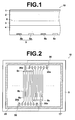
- Figure 1 is a partial sectional view of a radiation image detector in an embodiment of the present invention;
- Figure 2 is a plan view of the radiation image detector illustrated in Figure 1;
- Figure 3A is a diagram for explaining action for recording a radiation image in the radiation image detector illustrated in Figure 1;
- Figure 3B is a diagram for explaining action for recording a radiation image in the radiation image detector illustrated in Figure 1;
- Figure 4 is a diagram for explaining action for reading out a radiation image from the radiation image detector illustrated in Figure 1; and
- Figure 5 is a diagram illustrating the configuration of a radiation image detector according to the related art.
- Hereinafter, an embodiment of a radiation image detector according to the present invention will be described with reference to the attached drawings. Figure 1 is a diagram illustrating a partial sectional view of the radiation image detector of the present invention.
- In a
radiation image detector 10 according to the present invention, afirst electrode layer 1, aphotoconductive layer 2 for recording, acharge transport layer 3, aphotoconductive layer 4 for readout and asecond electrode layer 5 are superposed one on another in this order, as illustrated in Figure 1. Thefirst electrode layer 1 transmits radiation which carries a radiation image. Thephotoconductive layer 2 for recording generates electric charge by irradiation with the radiation transmitted through thefirst electrode layer 1. Thecharge transport layer 3 acts as an insulator against electric charge of one of the polarities of the electric charges generated in thephotoconductive layer 2 for recording. Thecharge transport layer 3 also acts as a conductor of electric charge of the opposite polarity. Thephotoconductive layer 4 for readout generates electric charge by irradiation with readout light. Thesecond electrode layer 5 includes a plurality of firstlinear electrodes 5a which transmit readout light and a plurality of secondlinear electrodes 5b which block the readout light. Each of the plurality of secondlinear electrodes 5b is provided between the plurality of firstlinear electrodes 5a. Further, acharge storage portion 6 is formed between thephotoconductive layer 2 for recording and thecharge transport layer 3. Thecharge storage portion 6 stores electric charge generated in thephotoconductive layer 2 for recording. These layers are superposed on a glass substrate sequentially from thesecond electrode layer 5. However, in Figure 1, the glass substrate is omitted. - As the
first electrode layer 1, any kind of material which transmits radiation may be used. For example, a so-called NESA coating (SnO2), an ITO (Indium Tin Oxide) coating, an IDIXO (Idemitsu Indium X-metal Oxide, manufactured by Idemitsu Kosan Co., Ltd.) coating, which is an amorphous light-transmissive oxide coating, or the like may be used by forming thereinto a layer which has a thickness within the range of 50 to 200nm. Alternatively, coating made of Al, Au or the like which has a thickness of 100nm may be used. - The
second electrode layer 5 includes the firstlinear electrodes 5a and the secondlinear electrodes 5b, as described above. In thesecond electrode layer 5, each of the firstlinear electrodes 5a and each of the secondlinear electrodes 5b are alternately arranged in parallel with a predetermined space therebetween. - The first
linear electrode 5a is made of a conductive material which transmits readout light. Any kind of conductive material which transmits readout light may be used as the material for the firstlinear electrode 5a. For example, a material, such as ITO or IDIXO, may be used in a manner similar to formation of thefirst electrode layer 1. Alternatively, metal, such as Al or Cr, may be formed into an electrode which has an appropriate thickness (for example, approximately 10nm) for transmitting readout light. - The second
linear electrode 5b is made of a conductive material which blocks readout light. Any kind of conductive material which blocks readout light may be used as the material for the secondlinear electrode 5b. For example, metal, such as Al or Cr, which blocks the readout light, may be formed into an electrode which has a sufficient thickness for blocking the readout light. - The
photoconductive layer 2 for recording should generate electric charge by irradiation with radiation. As the material for thephotoconductive layer 2, a material containing a-Se as its main component is used. The a-Se is advantageous in that it has relatively high quantum efficiency for radiation, high dark resistance or the like. An appropriate thickness of thephotoconductive layer 2 for recording is approximately 500µm. - As a material for the
charge transport layer 3, it is preferable that a difference between the mobility of electric charge charged in thefirst electrode layer 1 during recording of a radiation image and that of electric charge which has an opposite polarity to that of the electric charge charged in thefirst electrode layer 1 is as large as possible (for example, more than or equal to 102, and preferably, more than or equal to 103). As the material for thecharge transport layer 3, an organic compound, such as poly-N-vinylcarbazole(PVK), N,N'-diphenyl-N,N'-bis(3-methylphenyl)-[1,1'-biphenyl]-4,4'-diamine (TPD) or a discotic liquid crystal, or a semiconductor, such as a dispersion of TPD in polymer (polycarbonate, polystyrene or PVK) or a-Se doped with 10 to 200ppm of Cl, is appropriate. - As a material for the
photoconductive layer 4 for readout, a material which exhibits conductivity by irradiation with readout light or erasing light should be used. For example, a photoconductive material which contains one of a-Se, Se-Te, Se-As-Te, metal-free phthalocyanine, metal phthalocyanine, MgPc (Magnesium phthalocyanine), VoPc (phase II of Vanadyl phthalocyanine) and CuPc (Copper phthalocyanine) as its main component is preferable as the material for thephotoconductive layer 4 for readout. Further, an appropriate thickness of thephotoconductive layer 4 for readout is within the range of approximately 0.1 to 1µm. - Next, Figure 2 is a plan view of the
radiation image detector 10 according to the present invention. In Figure 2, theradiation image detector 10 is viewed from thesecond electrode layer 5 side. - As illustrated in Figure 2, the
radiation image detector 10 includes aground pattern 20 to which the secondlinear electrodes 5b is connected. As illustrated in Figure 2, theground pattern 20 is formed in the periphery of theradiation image detector 10 so as to surround the firstlinear electrodes 5a and the secondlinear electrodes 5b. For example, theground pattern 20 should be made of a material, such as A1 or Cr, in a manner similar to formation of the secondlinear electrode 5b. In theradiation image detector 10 according to the present invention, theground pattern 20 has a ring shape. However, it is not necessary that theground pattern 20 has the ring shape. The shape of theground pattern 20 may be a shape in which a part of a ring is removed. The shape of theground pattern 20 may be any shape which is formed in the periphery of the secondlinear electrodes 5b, and to which all of the secondlinear electrodes 5b are connected. It is preferable that theground pattern 20 surrounds all of the firstlinear electrodes 5a and all of the secondlinear electrodes 5b so as to reduce external noise entering the firstlinear electrodes 5a. - In the
radiation image detector 10 according to the present invention, an end of each of a plurality oflinear electrode arrays 5c, each including a predetermined plurality of second linear electrodes adjacent to each other, is connected to theground pattern 20. The plurality oflinear electrode arrays 5c is connected to theground pattern 20 so that the end of each of the plurality of linear electrode arrays, connected to theground pattern 20, is opposite to the end of a linear electrode array adjacent to each of the plurality of linear electrode arrays, connected to theground pattern 20. - Further, a
charge amplifier IC 30 is connected to the firstlinear electrode 5a so as to detect an electric signal flows into the firstlinear electrode 5a. Further, anamplifier ground portion 20a, to which a ground terminal of thecharge amplifier IC 30 is connected, is formed in theground pattern 20. In theradiation image detector 10 according to the present invention, a rectangularamplifier ground portion 20a is formed, as illustrated in Figure 2. However, it is not necessary that the shape of theamplifier ground portion 20a is rectangular. A part of the ring-shapedground pattern 20 may be utilized as theamplifier ground portion 20a. - Next, the action of the radiation image detector according to the present invention will be described.
- First, as illustrated in Figure 3A, negative voltage is applied to the
first electrode layer 1 in theradiation image detector 10 from a high voltage source. In this state, a subject is irradiated with radiation emitted from a radiation source, and the radiation is transmitted through the subject. Accordingly, theradiation image detector 10 is irradiated with radiation carrying a radiation image of the subject from thefirst electrode layer 1 side of theradiation image detector 10. At this time, both of the firstlinear electrodes 5a and the secondlinear electrodes 5b are grounded. - Then, the radiation projected onto the
radiation image detector 10 is transmitted through thefirst electrode layer 1, and thephotoconductive layer 2 for recording is irradiated with the radiation. Then, a pair of electric charges is generated in thephotoconductive layer 2 for recording by irradiation with the radiation. Then, a positive electric charge in the pair of electric charges bonds with a negative charge charged in thefirst electrode layer 1, and the positive electric charge disappears. A negative electric charge in the pair of electric charges is stored, as latent image electric charge, in thestorage portion 6 formed at the interface between thephotoconductive layer 2 for recording and the charge transport layer 3 (please refer to Figure 3B). - Then, as illustrated in Figure 4, the
radiation image detector 10 is irradiated with readout light L1 from thesecond electrode layer 5 side in a state in which thefirst electrode layer 1 and the secondlinear electrode 5b are grounded. The readout light L1 is transmitted through the firstlinear electrode 5a and thephotoconductive layer 4 for readout is irradiated with the readout light L1. When thephotoconductive layer 4 is irradiated with the readout light L1, a pair of electric charges is generated in thephotoconductive layer 4 for readout. Then, a positive charge in the pair of electric charges bonds with latent image electric charge in thestorage portion 6. Further, a negative charge in the pair of electric charges bonds with a positive charge charged in the firstlinear electrode 5a in thesecond electrode layer 5. - Since the positive electric charge and the negative electric charge bond with each other, as described above, an electric current flows into the first
linear electrode 5a and each ofcharge amplifiers 31 in thecharge amplifier IC 30. Then, the electric current is detected as an image signal by obtaining the integral of the electric current. Accordingly, an image signal based on the radiation image is read out. - In the
radiation image detector 10 according to the present invention, theground pattern 20 is formed in the periphery of thesecond electrode layer 5 so as to surround the firstlinear electrodes 5a and the secondlinear electrode 5b. Further, the secondlinear electrodes 5b are connected to theground pattern 20. Therefore, even if one of the secondlinear electrodes 5b is disconnected, the other secondlinear electrodes 5b are grounded through theground pattern 20. Therefore, it is possible to maintain common ground electric potential at the secondlinear electrodes 5b. - Further, since the
ground pattern 20 is formed so as to surround the firstlinear electrodes 5a, it is possible to guard the first linear electrodes against external noise. Therefore, it is possible to improve the image quality of a readout radiation image. - Further, since the
amplifier ground portion 20a, to which the ground terminal of thecharge amplifier IC 30 is connected, is formed in theground pattern 20, it is possible to supply stable ground electric potential to thecharge amplifiers 31. - Further, in the aforementioned embodiment, the present invention is applied to a radiation image detector which adopts a so-called direct conversion method. The direct conversion method is a method, in which a radiation image is recorded by being irradiated with radiation and by directly converting the radiation into electric charge. However, it is not necessary that the radiation image detector is a radiation image detector adopting the direct conversion method. The present invention may be applied to a radiation image detector which adopts another method, such as a so-called indirect conversion method. The indirect conversion method is a method, in which a radiation image is recorded by temporarily converted radiation into visible light and by converting the visible light into electric charge.
- Further, it is not necessary that the layers of the radiation image detector according to the present invention are structured as described in the above embodiment. An additional layer or layers may be added to the layers.
Claims (4)
- A radiation image detector comprising:an electric charge generation layer (2) for generating electric charge by irradiation with an electromagnetic wave for recording which carries a radiation image; andan electrode layer (5) including a multiplicity of first linear electrodes (5a) connected to a detection unit (30) for detecting the electric charge generated in the electric charge generation layer as an electric signal and a multiplicity of second linear electrodes (5b) which is grounded, wherein each of the multiplicity of first linear electrodes (5a) and each of the multiplicity of second linear electrodes (5b) are alternately arranged parallel to each other with a predetermined space therebetween, and wherein the electric charge generation layer (2) and the electrode layer (5) are superposed one on the other in this order, characterized in that a ground pattern (20) is formed in the periphery of the electrode layer (5), and wherein the multiplicity of second linear electrodes (5b) is connected to the ground pattern (20).
- A radiation image detector, as defined in Claim 1, characterized in that the ground pattern (20) is formed so as to surround the multiplicity of first linear electrodes (5a) and the multiplicity of second linear electrodes (5b).
- A radiation image detector, as defined in Claim 1 or 2, characterized in that an end of each of a plurality of linear electrode arrays (5c), each including a predetermined plurality of second linear electrodes (5b) adjacent to each other, is connected to the ground pattern (20), and wherein the end of each of the plurality of linear electrode arrays (5c), connected to the ground pattern (20), is opposite to the end of a linear electrode array (5c) adjacent to each of the plurality of linear electrode arrays, connected to the ground pattern (20).
- A radiation image detector, as defined in any one of Claims 1 through 3, characterized in that the detection unit (30) is a charge amplifier IC (integrated circuit) (30), and wherein the ground pattern (20) includes an amplifier ground portion (20a) to which a ground terminal of the charge amplifier IC (30) is connected.
Applications Claiming Priority (1)
| Application Number | Priority Date | Filing Date | Title |
|---|---|---|---|
| JP2005202837A JP2007027179A (en) | 2005-07-12 | 2005-07-12 | Radiation image detector |
Publications (2)
| Publication Number | Publication Date |
|---|---|
| EP1744367A2 true EP1744367A2 (en) | 2007-01-17 |
| EP1744367A3 EP1744367A3 (en) | 2010-07-07 |
Family
ID=37076086
Family Applications (1)
| Application Number | Title | Priority Date | Filing Date |
|---|---|---|---|
| EP06014454A Withdrawn EP1744367A3 (en) | 2005-07-12 | 2006-07-12 | Radiation image detector |
Country Status (3)
| Country | Link |
|---|---|
| US (1) | US20080006787A1 (en) |
| EP (1) | EP1744367A3 (en) |
| JP (1) | JP2007027179A (en) |
Family Cites Families (12)
| Publication number | Priority date | Publication date | Assignee | Title |
|---|---|---|---|---|
| FR2646516A1 (en) * | 1989-04-28 | 1990-11-02 | Cgr Mev | IONIZING RADIATION PHOTOCONDUCTIVE DETECTORS AND METHODS OF IMPLEMENTING SAME |
| JPH03183158A (en) * | 1989-12-12 | 1991-08-09 | Mitsubishi Electric Corp | Input/output buffer circuit |
| GB2318448B (en) * | 1996-10-18 | 2002-01-16 | Simage Oy | Imaging detector and method of production |
| JP4040201B2 (en) * | 1999-03-30 | 2008-01-30 | 富士フイルム株式会社 | Radiation solid state detector, and radiation image recording / reading method and apparatus using the same |
| US6590224B2 (en) * | 2000-03-22 | 2003-07-08 | Fuji Photo Film Co., Ltd. | Image storage medium and method of manufacturing the same |
| JP4091334B2 (en) * | 2001-05-11 | 2008-05-28 | 富士フイルム株式会社 | Image recording method and apparatus, and image recording medium |
| EP1262797B1 (en) * | 2001-05-11 | 2011-07-13 | FUJIFILM Corporation | Method and apparatus for image recording and image recording medium |
| JP3481935B2 (en) * | 2001-07-02 | 2003-12-22 | Necエレクトロニクス株式会社 | Semiconductor integrated circuit having macro cell and design method thereof |
| JP3932857B2 (en) * | 2001-10-22 | 2007-06-20 | 株式会社島津製作所 | Radiation detector |
| JP2004342691A (en) * | 2003-05-13 | 2004-12-02 | Fuji Photo Film Co Ltd | Radiation image detector |
| JP2004363463A (en) * | 2003-06-06 | 2004-12-24 | Fuji Photo Film Co Ltd | Radiation image detector |
| JP2005183671A (en) * | 2003-12-19 | 2005-07-07 | Fuji Photo Film Co Ltd | Radiation image detector |
-
2005
- 2005-07-12 JP JP2005202837A patent/JP2007027179A/en not_active Abandoned
-
2006
- 2006-07-12 EP EP06014454A patent/EP1744367A3/en not_active Withdrawn
- 2006-07-12 US US11/484,618 patent/US20080006787A1/en not_active Abandoned
Also Published As
| Publication number | Publication date |
|---|---|
| US20080006787A1 (en) | 2008-01-10 |
| JP2007027179A (en) | 2007-02-01 |
| EP1744367A3 (en) | 2010-07-07 |
Similar Documents
| Publication | Publication Date | Title |
|---|---|---|
| WO2014069818A1 (en) | X-ray detector and x-ray detection system | |
| US8581198B2 (en) | Apparatus and method for detecting radiation | |
| EP1744367A2 (en) | Radiation image detector | |
| US7294847B2 (en) | Radiographic image detector | |
| US20050184244A1 (en) | Radiation detector and light or radiation detector | |
| US7728300B2 (en) | Radiation image detector | |
| EP1286182A1 (en) | Solid state radiation detector | |
| US8415634B2 (en) | Apparatus and method for detecting radiation | |
| EP4235226A1 (en) | Radiation detector and detection method | |
| EP1262797B1 (en) | Method and apparatus for image recording and image recording medium | |
| EP2624316A1 (en) | Radiation detector and method for detecting radiation | |
| US7482614B2 (en) | Radiation image detector | |
| JP5270121B2 (en) | Imaging device | |
| US7196344B2 (en) | Solid state radiation detector and method for testing the same | |
| JP2008128725A (en) | Radiographic image reading method and radiographic image detector | |
| JP2008089491A (en) | Radiation image detector | |
| US7365353B2 (en) | Radiation image detector | |
| JP2003163340A (en) | Solid state detector | |
| US20070057193A1 (en) | Radiation image detector | |
| JP2003218335A (en) | Solid state detector | |
| JP2008177216A (en) | Radiation image detector | |
| JP2001284565A (en) | Image detector | |
| JP2007304510A (en) | Radiation image recording / reading apparatus | |
| JP2007208162A (en) | Radiation image detection device | |
| JP2003086781A (en) | Solid-state radiation detector |
Legal Events
| Date | Code | Title | Description |
|---|---|---|---|
| PUAI | Public reference made under article 153(3) epc to a published international application that has entered the european phase |
Free format text: ORIGINAL CODE: 0009012 |
|
| AK | Designated contracting states |
Kind code of ref document: A2 Designated state(s): AT BE BG CH CY CZ DE DK EE ES FI FR GB GR HU IE IS IT LI LT LU LV MC NL PL PT RO SE SI SK TR |
|
| AX | Request for extension of the european patent |
Extension state: AL BA HR MK YU |
|
| RAP1 | Party data changed (applicant data changed or rights of an application transferred) |
Owner name: FUJIFILM CORPORATION |
|
| PUAL | Search report despatched |
Free format text: ORIGINAL CODE: 0009013 |
|
| AK | Designated contracting states |
Kind code of ref document: A3 Designated state(s): AT BE BG CH CY CZ DE DK EE ES FI FR GB GR HU IE IS IT LI LT LU LV MC NL PL PT RO SE SI SK TR |
|
| AX | Request for extension of the european patent |
Extension state: AL BA HR MK RS |
|
| AKY | No designation fees paid | ||
| STAA | Information on the status of an ep patent application or granted ep patent |
Free format text: STATUS: THE APPLICATION IS DEEMED TO BE WITHDRAWN |
|
| 18D | Application deemed to be withdrawn |
Effective date: 20110108 |