EP1742367A1 - Phasenregelkreisschaltung - Google Patents
Phasenregelkreisschaltung Download PDFInfo
- Publication number
- EP1742367A1 EP1742367A1 EP05291442A EP05291442A EP1742367A1 EP 1742367 A1 EP1742367 A1 EP 1742367A1 EP 05291442 A EP05291442 A EP 05291442A EP 05291442 A EP05291442 A EP 05291442A EP 1742367 A1 EP1742367 A1 EP 1742367A1
- Authority
- EP
- European Patent Office
- Prior art keywords
- filter
- electric signal
- output
- phase detector
- input
- Prior art date
- Legal status (The legal status is an assumption and is not a legal conclusion. Google has not performed a legal analysis and makes no representation as to the accuracy of the status listed.)
- Withdrawn
Links
- 230000003321 amplification Effects 0.000 claims abstract description 6
- 238000003199 nucleic acid amplification method Methods 0.000 claims abstract description 6
- 239000003990 capacitor Substances 0.000 description 4
- 238000010586 diagram Methods 0.000 description 4
- 230000003247 decreasing effect Effects 0.000 description 1
Images


Classifications
-
- H—ELECTRICITY
- H03—ELECTRONIC CIRCUITRY
- H03L—AUTOMATIC CONTROL, STARTING, SYNCHRONISATION OR STABILISATION OF GENERATORS OF ELECTRONIC OSCILLATIONS OR PULSES
- H03L7/00—Automatic control of frequency or phase; Synchronisation
- H03L7/06—Automatic control of frequency or phase; Synchronisation using a reference signal applied to a frequency- or phase-locked loop
- H03L7/08—Details of the phase-locked loop
- H03L7/10—Details of the phase-locked loop for assuring initial synchronisation or for broadening the capture range
- H03L7/107—Details of the phase-locked loop for assuring initial synchronisation or for broadening the capture range using a variable transfer function for the loop, e.g. low pass filter having a variable bandwidth
-
- H—ELECTRICITY
- H03—ELECTRONIC CIRCUITRY
- H03L—AUTOMATIC CONTROL, STARTING, SYNCHRONISATION OR STABILISATION OF GENERATORS OF ELECTRONIC OSCILLATIONS OR PULSES
- H03L2207/00—Indexing scheme relating to automatic control of frequency or phase and to synchronisation
- H03L2207/06—Phase locked loops with a controlled oscillator having at least two frequency control terminals
-
- H—ELECTRICITY
- H03—ELECTRONIC CIRCUITRY
- H03L—AUTOMATIC CONTROL, STARTING, SYNCHRONISATION OR STABILISATION OF GENERATORS OF ELECTRONIC OSCILLATIONS OR PULSES
- H03L7/00—Automatic control of frequency or phase; Synchronisation
- H03L7/06—Automatic control of frequency or phase; Synchronisation using a reference signal applied to a frequency- or phase-locked loop
- H03L7/08—Details of the phase-locked loop
- H03L7/099—Details of the phase-locked loop concerning mainly the controlled oscillator of the loop
- H03L7/0995—Details of the phase-locked loop concerning mainly the controlled oscillator of the loop the oscillator comprising a ring oscillator
Definitions
- the present invention refers to a phase locked loop circuit.
- Phase locked loop circuits or PLL circuits are known in the state of the art which are employed in numerous electronic appliances as, for example, in modulators or demodulators of medium frequency signals or FM signals.
- a PLL circuit comprises a phase detector having in input a reference frequency and a frequency deriving from a voltage controlled oscillator or VCO, a filter having in input the output signal of the phase detector and outputting a signal in input to the VCO.
- a very important parameter of the PLL circuits is the lock time, that is the time period employed by the circuit to obtain that the output frequency of the VCO becomes equal to the reference frequency.
- the lock time is inversely proportional to the bandwidth of the circuit; for the PLL circuits used, for example, in FM modulators where the bandwidth of the PLL circuit is about 10Hz, the lock time is high, that is of some seconds.
- the output frequency changes thereby producing interferences in adjacent channels, in the case of a multi-channel FM modulator, and it produces higher noise in the receiver channel.
- the lock time should be kept low for reducing said perturbations.
- a known circuit that allows to lower the lock time is the PLL circuit which uses a charge pump as shown in Figure 1.
- Said circuit comprises a digital phase/frequency detector or PFD (Phase Frequency Detector) 4 having in input a digital reference frequency Fref1 and a digital frequency fv and which has two outputs UP and DOWN to be enabled if the reference frequency Fref1 is higher or lower than the frequency fv.
- the two outputs UP and DOWN control respective current generators adapted to send a current to a filter 1 having a narrow bandwidth; the phase detector 4 and the current generators act as a current pump charge.
- the output voltage signal of the filter 1 is the control signal of the VCO 2 the output frequency of Fout which is in input to a frequency divider 3 for obtaining the frequency fv.
- the increase of the current in input to the filter allows an increase of the bandwidth of the filter 1 and a decrease of the lock time. After the lock phase the charge pump's current is turned back to its normal value to assure the stability of the PLL circuit.
- Said circuit is of easy design and the charge pump's current can be controlled easily by means of a microcontroller; however, the circuit has a reduced stability both in the lock phase and during the other successive phases and it is also difficult to optimise the current boost time for reducing the lock time to its minimum.
- US patent 5631601 Another circuit solution with a PLL is described in US patent 5631601 .
- Said patent discloses a PLL circuit adapted to demodulate a FM carrier wave; the circuit comprises a phase detector and a VCO having in input the output signal of the phase detector and adapted to provide a signal in input to the phase detector for comparison with said FM carrier wave.
- the PLL circuit comprises a variable gain circuit operable to select a desired gain for the PLL and to select a bandwidth for demodulation by the circuit.
- the circuit of the US patent 5631601 comprises a synthesizer adapted to regulate the PLL at a given frequency; the synthesizer provides a voltage signal in input to the VCO to bring the output frequency of the VCO equal to that of the required carrier.
- the synthesizer is a circuital element which is of complex provision and requires the use of a determined space in the chip wherein the PLL is implemented.
- phase locked loop circuit comprising a phase detector having a first input for receiving a first frequency signal and an output, a first filter adapted to filter the output electric signal of said phase detector, a voltage controlled oscillator adapted to generate a second frequency signal in response to the output filtered signal of said phase detector, said phase detector having a second input for receiving said second frequency signal and being adapted to compare it with said first frequency signal, characterized by comprising means adapted to amplify the difference between an electric signal coupled with the output of the phase detector and a reference electric signal and a second filter adapted to receive the output electric signal of said amplification means and to send an output electric signal to said voltage controlled oscillator, said circuit comprising further means adapted to modify the value of the electric signal in input to said second filter to decrease the response time of said second filter.
- phase locked loop circuit according to a first embodiment of the present invention.
- Said circuit comprises a phase detector 10 having in input a reference frequency fref and a frequency fo deriving from a frequency divider 20 having an input frequency fvco deriving from a voltage controlled oscillator or VCO 30.
- the phase detector 10 comprises a known phase/frequency detector or PFD 11 of the digital type which has two outputs UP and DOWN to be enabled if the reference frequency fref is higher or lower than the frequency fo.
- Two outputs UP and DOWN control respective current generators I1 and I2 arranged along a circuit line between a supply voltage VDD and ground; the phase detector 10 generates an output voltage signal Vcp.
- the phase detector 10 comprises a charge pump, for example, a Gilbert's cell.
- the signal Vcp in a first circuit path, is in input to a filter 40 having a given bandwidth, the output signal V40 of which is in input to the VCO 30.
- the filter 40 can be formed by means of a first circuit line in parallel with a second circuit line which are arranged between the voltage Vcp and ground GND; the first circuit line comprises a resistance and a capacitor while the second circuit line comprises a capacitor.
- the filter 40 can be formed even by means of a resistance in parallel with a capacitor, which are arranged between a voltage Vcp and a circuit node, and a resistance arranged between said circuital node and ground GND.
- the circuit in Figure 2 comprises means 50 adapted to amplify the difference between an electric signal coupled with the output of the phase detector and a second filter 60 adapted to receiver the output electric signal of said amplification means 50 and adapted to send an output electric signal V60 to said voltage controlled oscillator 30; preferably the second filter 60 has a bandwidth smaller than that of the first filter 40 to assure the stability of the phase locked loop circuit.
- the signal Vcp and a reference signal Vref are in input to a transconductance amplifier 50.
- the amplifier 50 generates a current signal 150 if the signal Vcp is different from the signal Vref.
- the signal I50 is adapted to charge the filter 60 having a bandwidth smaller than the bandwidth of the filter 40, preferably with a rate of 10/20 with respect to the bandwidth of the filter 40; this to assure the stability of the PLL circuit.
- the filter 60 generates a signal V60 in input to the VCO 30.
- the filter 60 can be formed by means of a capacitor connected between ground GND and the circuit line through which the current 150 passes.
- the VCO 30 receives the signals V60 and V40 in output from the filters 60 and 40 and produces the frequency fvco.
- the circuit in Figure 2 comprises means 100 adapted to modify the value of the electric signal in input to the filter 60 to decrease its response time, that is to change faster the value of the electric signal V60 in output from the filter 60; particularly the means 100 are adapted to change the current 150 in input to the filter 60 if the absolute value of the difference between the signal Vcp and the reference signal Vref is higher than a given value Vf, which is for example 0.2 Volt.
- the amplifier 50 does not supply current to the filter 60 and the voltage V60 is kept constant. Small variations of the frequency fvco in output from the VCO 30 are corrected by means of the loop formed by the phase detector 10, the filter 40, the VCO 30 and the frequency divider 20.
- the voltage Vcp is different from the voltage Vref; the amplifier 50 sends a current 150 to the filter 60 to charge it and to obtain a fast response; the value of the voltage V60 is changed faster and arrives faster to the VCO 30.
- the means 100 increase or decrease the current in input to the filter 60 to obtain a response in shorter time. In such a way the voltage V60 is changed in a short time.
- the means 100 comprises a window comparator 101 adapted to compare the voltages Vref and Vcp and to send a signal Boost to the amplifier 50 if the voltage Vcp-Vref is higher than Vf or is lower than -Vf.
- the signal Boost acts on the amplifier to increase the transconductance gain Gm.
- the current 150 will be higher in absolute value so that the filter 60 responds faster and the new voltage V60 is sent faster to the VCO 30. This allows to decrease the lock time Tc with respect to the PLL circuit of prior art.
- FIG 3 a phase locked loop circuit according to a second embodiment of the invention is shown.
- the only difference of the circuit in Figure 3 with respect to the circuit of the first embodiment shown in Figure 2 is the different circuit structure of the means 100.
- the last comprises a window comparator 101 adapted to compare the voltage Vcp and Vref and a circuit line arranged between a supply voltage Vcc and ground GND which comprises a switch SW1, the series of two resistances R1 and R2 and a switch SW2; the output terminal of the amplifier 50 and the input of the filter 60 are connected with the intermediate node between the resistances R1 and R2.
- the comparator 101 closes the switch SW2 and opens the switch SW1 while if the voltage Vcp-Vref is higher than Vf the comparator 101 closes the switch SW1 and opens the switch SW2 .
- the current 160 in input to the filter 60 will be higher than the current 150 in output from the amplifier 50 without the use of said circuit line, so that the filter 60 responds faster and the new voltage V60 is sent faster to the VCO 30. This allows a decrease of the lock time Tc with respect to the known PLL circuits.
- both the amplifier 50 and the means 100 have in input the voltage V40 in the place of the voltage Vcp.
- Figures 4 and 5 show the time diagrams of the voltages V40-Vref and V60-Vref and the frequency fvco for the phase locked loop circuit in Figure 2 without the use of the means 100. It is noticed thet the settling time or lock time is about 1.5 s.
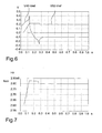
- Figures 6 and 7 show the time diagrams of the voltages V40-Vref and V60-Vref and the frequency fvco for the phase locked loop circuit in Figure 2 with the use of the means 100. It is noticed that the settling time or lock time is decreased and it is about 0.5 s.
Landscapes
- Stabilization Of Oscillater, Synchronisation, Frequency Synthesizers (AREA)
Priority Applications (2)
| Application Number | Priority Date | Filing Date | Title |
|---|---|---|---|
| EP05291442A EP1742367A1 (de) | 2005-06-30 | 2005-06-30 | Phasenregelkreisschaltung |
| US11/480,757 US7408418B2 (en) | 2005-06-30 | 2006-06-30 | Phase locked loop circuit having reduced lock time |
Applications Claiming Priority (1)
| Application Number | Priority Date | Filing Date | Title |
|---|---|---|---|
| EP05291442A EP1742367A1 (de) | 2005-06-30 | 2005-06-30 | Phasenregelkreisschaltung |
Publications (1)
| Publication Number | Publication Date |
|---|---|
| EP1742367A1 true EP1742367A1 (de) | 2007-01-10 |
Family
ID=34981496
Family Applications (1)
| Application Number | Title | Priority Date | Filing Date |
|---|---|---|---|
| EP05291442A Withdrawn EP1742367A1 (de) | 2005-06-30 | 2005-06-30 | Phasenregelkreisschaltung |
Country Status (2)
| Country | Link |
|---|---|
| US (1) | US7408418B2 (de) |
| EP (1) | EP1742367A1 (de) |
Families Citing this family (4)
| Publication number | Priority date | Publication date | Assignee | Title |
|---|---|---|---|---|
| US7986926B2 (en) * | 2006-09-27 | 2011-07-26 | Silicon Laboratories Inc. | Integrating an FM transmitter into a cellular telephone |
| US10291389B1 (en) * | 2018-03-16 | 2019-05-14 | Stmicroelectronics International N.V. | Two-point modulator with matching gain calibration |
| US10749532B1 (en) * | 2019-03-04 | 2020-08-18 | Xilinx, Inc. | Method and apparatus for a phase locked loop circuit |
| CN116979960A (zh) * | 2022-04-22 | 2023-10-31 | 罗德施瓦兹两合股份有限公司 | 锁相环电路、电子电路装置和电子设备 |
Citations (4)
| Publication number | Priority date | Publication date | Assignee | Title |
|---|---|---|---|---|
| US5382922A (en) * | 1993-12-23 | 1995-01-17 | International Business Machines Corporation | Calibration systems and methods for setting PLL gain characteristics and center frequency |
| US5631601A (en) | 1993-09-29 | 1997-05-20 | Sgs-Thomson Microelectronics Limited | FM demodulation with a variable gain phase locked loop |
| DE19917585A1 (de) * | 1999-04-19 | 2000-11-30 | Siemens Ag | Fanghilfe in Phasenregelkreisen mit integralem Loopfilter |
| US6826246B1 (en) * | 1999-10-15 | 2004-11-30 | Agere Systems, Inc. | Phase locked loop with control voltage centering |
Family Cites Families (1)
| Publication number | Priority date | Publication date | Assignee | Title |
|---|---|---|---|---|
| US6476681B1 (en) * | 1998-08-11 | 2002-11-05 | Denso International America, Inc. | Adjustable bandwidth phase locked loop with fast settling time |
-
2005
- 2005-06-30 EP EP05291442A patent/EP1742367A1/de not_active Withdrawn
-
2006
- 2006-06-30 US US11/480,757 patent/US7408418B2/en active Active
Patent Citations (4)
| Publication number | Priority date | Publication date | Assignee | Title |
|---|---|---|---|---|
| US5631601A (en) | 1993-09-29 | 1997-05-20 | Sgs-Thomson Microelectronics Limited | FM demodulation with a variable gain phase locked loop |
| US5382922A (en) * | 1993-12-23 | 1995-01-17 | International Business Machines Corporation | Calibration systems and methods for setting PLL gain characteristics and center frequency |
| DE19917585A1 (de) * | 1999-04-19 | 2000-11-30 | Siemens Ag | Fanghilfe in Phasenregelkreisen mit integralem Loopfilter |
| US6826246B1 (en) * | 1999-10-15 | 2004-11-30 | Agere Systems, Inc. | Phase locked loop with control voltage centering |
Also Published As
| Publication number | Publication date |
|---|---|
| US20070018735A1 (en) | 2007-01-25 |
| US7408418B2 (en) | 2008-08-05 |
Similar Documents
| Publication | Publication Date | Title |
|---|---|---|
| US6549599B2 (en) | Stable phase locked loop having separated pole | |
| US8378725B2 (en) | Adaptive bandwidth phase-locked loop | |
| US20060006914A1 (en) | Method of implementing multi-transfer curve phase lock loop | |
| US20090237131A1 (en) | Phase locked loop | |
| US7312663B2 (en) | Phase-locked loop having a bandwidth related to its input frequency | |
| WO2009109636A2 (en) | Phase-locked loop | |
| WO2009109637A2 (en) | Phase-locked loop | |
| US7180377B1 (en) | Method and apparatus for a hybrid phase lock loop frequency synthesizer | |
| US20090146704A1 (en) | Delay locked loop circuit and method for eliminating jitter and offset therein | |
| US6759838B2 (en) | Phase-locked loop with dual-mode phase/frequency detection | |
| US8264258B1 (en) | Phase lock loop circuit | |
| CN110417405A (zh) | 具有降低的vco增益的锁相环设计 | |
| US6211743B1 (en) | Phase-locked loop having temperature-compensated bandwidth control | |
| US8760201B1 (en) | Digitally programmed capacitance multiplication with one charge pump | |
| US10447253B2 (en) | High performance PLL based on PVT independent stable oscillator | |
| US7408418B2 (en) | Phase locked loop circuit having reduced lock time | |
| US8810291B2 (en) | Phase-locked loop | |
| JP2006527936A (ja) | フェーズ・ロックト・ループ・フィルタ | |
| US20070229175A1 (en) | Phase lock loop circuit | |
| KR100918860B1 (ko) | 루프필터 보상회로를 구비하는 주파수 합성기 | |
| JP2005260866A (ja) | フラクショナルn周波数シンセサイザ装置 | |
| JP2001320235A (ja) | 電圧制御発振器 | |
| Han et al. | A time-constant calibrated phase-locked loop with a fast-locked time | |
| US20070237277A1 (en) | Method and Integrated Circuit for Controlling an Oscillator Signal | |
| US7123065B1 (en) | Method of improving lock acquisition times in systems with a narrow frequency range |
Legal Events
| Date | Code | Title | Description |
|---|---|---|---|
| PUAI | Public reference made under article 153(3) epc to a published international application that has entered the european phase |
Free format text: ORIGINAL CODE: 0009012 |
|
| AK | Designated contracting states |
Kind code of ref document: A1 Designated state(s): AT BE BG CH CY CZ DE DK EE ES FI FR GB GR HU IE IS IT LI LT LU MC NL PL PT RO SE SI SK TR |
|
| AX | Request for extension of the european patent |
Extension state: AL BA HR LV MK YU |
|
| 17P | Request for examination filed |
Effective date: 20070621 |
|
| 17Q | First examination report despatched |
Effective date: 20070712 |
|
| AKX | Designation fees paid |
Designated state(s): DK FR GB IT |
|
| REG | Reference to a national code |
Ref country code: DE Ref legal event code: 8566 |
|
| STAA | Information on the status of an ep patent application or granted ep patent |
Free format text: STATUS: THE APPLICATION IS DEEMED TO BE WITHDRAWN |
|
| 18D | Application deemed to be withdrawn |
Effective date: 20071123 |