EP1742246A2 - Plasma display panel and method of manufacturing the same - Google Patents
Plasma display panel and method of manufacturing the same Download PDFInfo
- Publication number
- EP1742246A2 EP1742246A2 EP06253443A EP06253443A EP1742246A2 EP 1742246 A2 EP1742246 A2 EP 1742246A2 EP 06253443 A EP06253443 A EP 06253443A EP 06253443 A EP06253443 A EP 06253443A EP 1742246 A2 EP1742246 A2 EP 1742246A2
- Authority
- EP
- European Patent Office
- Prior art keywords
- powder
- barrier rib
- nano
- dielectric layer
- lower substrate
- Prior art date
- Legal status (The legal status is an assumption and is not a legal conclusion. Google has not performed a legal analysis and makes no representation as to the accuracy of the status listed.)
- Withdrawn
Links
- 238000004519 manufacturing process Methods 0.000 title claims abstract description 16
- 230000004888 barrier function Effects 0.000 claims abstract description 73
- 239000011858 nanopowder Substances 0.000 claims abstract description 42
- 239000000758 substrate Substances 0.000 claims description 59
- GWEVSGVZZGPLCZ-UHFFFAOYSA-N Titan oxide Chemical compound O=[Ti]=O GWEVSGVZZGPLCZ-UHFFFAOYSA-N 0.000 claims description 28
- 239000000843 powder Substances 0.000 claims description 24
- MCMNRKCIXSYSNV-UHFFFAOYSA-N Zirconium dioxide Chemical compound O=[Zr]=O MCMNRKCIXSYSNV-UHFFFAOYSA-N 0.000 claims description 22
- 239000011521 glass Substances 0.000 claims description 22
- 229910052751 metal Inorganic materials 0.000 claims description 17
- 239000002184 metal Substances 0.000 claims description 17
- 238000000034 method Methods 0.000 claims description 16
- 239000000463 material Substances 0.000 claims description 14
- 239000000203 mixture Substances 0.000 claims description 14
- 229910052802 copper Inorganic materials 0.000 claims description 8
- 229910052737 gold Inorganic materials 0.000 claims description 8
- 229910052759 nickel Inorganic materials 0.000 claims description 8
- 229910052763 palladium Inorganic materials 0.000 claims description 8
- 238000005530 etching Methods 0.000 claims description 7
- 150000002739 metals Chemical class 0.000 claims description 5
- 238000002310 reflectometry Methods 0.000 claims description 5
- 238000004381 surface treatment Methods 0.000 claims description 5
- 239000004020 conductor Substances 0.000 claims description 4
- 238000010304 firing Methods 0.000 claims description 3
- 239000003960 organic solvent Substances 0.000 claims description 2
- 238000002360 preparation method Methods 0.000 claims 1
- 230000008569 process Effects 0.000 description 10
- 230000006911 nucleation Effects 0.000 description 6
- 238000010899 nucleation Methods 0.000 description 6
- 239000000945 filler Substances 0.000 description 5
- 230000008901 benefit Effects 0.000 description 4
- PNEYBMLMFCGWSK-UHFFFAOYSA-N aluminium oxide Inorganic materials [O-2].[O-2].[O-2].[Al+3].[Al+3] PNEYBMLMFCGWSK-UHFFFAOYSA-N 0.000 description 3
- 229910052593 corundum Inorganic materials 0.000 description 3
- 238000010438 heat treatment Methods 0.000 description 3
- 230000003287 optical effect Effects 0.000 description 3
- 230000001681 protective effect Effects 0.000 description 3
- 229910001845 yogo sapphire Inorganic materials 0.000 description 3
- 230000000694 effects Effects 0.000 description 2
- 238000010297 mechanical methods and process Methods 0.000 description 2
- 238000012986 modification Methods 0.000 description 2
- 230000004048 modification Effects 0.000 description 2
- 238000011197 physicochemical method Methods 0.000 description 2
- 230000001154 acute effect Effects 0.000 description 1
- 239000003086 colorant Substances 0.000 description 1
- 230000006866 deterioration Effects 0.000 description 1
- 238000002845 discoloration Methods 0.000 description 1
- 230000006872 improvement Effects 0.000 description 1
- 239000012535 impurity Substances 0.000 description 1
- 239000011159 matrix material Substances 0.000 description 1
- 239000002245 particle Substances 0.000 description 1
- 238000000206 photolithography Methods 0.000 description 1
- 238000005488 sandblasting Methods 0.000 description 1
- 230000000007 visual effect Effects 0.000 description 1
Images


Classifications
-
- H—ELECTRICITY
- H01—ELECTRIC ELEMENTS
- H01J—ELECTRIC DISCHARGE TUBES OR DISCHARGE LAMPS
- H01J11/00—Gas-filled discharge tubes with alternating current induction of the discharge, e.g. alternating current plasma display panels [AC-PDP]; Gas-filled discharge tubes without any main electrode inside the vessel; Gas-filled discharge tubes with at least one main electrode outside the vessel
- H01J11/10—AC-PDPs with at least one main electrode being out of contact with the plasma
- H01J11/12—AC-PDPs with at least one main electrode being out of contact with the plasma with main electrodes provided on both sides of the discharge space
-
- H—ELECTRICITY
- H01—ELECTRIC ELEMENTS
- H01J—ELECTRIC DISCHARGE TUBES OR DISCHARGE LAMPS
- H01J11/00—Gas-filled discharge tubes with alternating current induction of the discharge, e.g. alternating current plasma display panels [AC-PDP]; Gas-filled discharge tubes without any main electrode inside the vessel; Gas-filled discharge tubes with at least one main electrode outside the vessel
- H01J11/20—Constructional details
- H01J11/22—Electrodes, e.g. special shape, material or configuration
-
- H—ELECTRICITY
- H01—ELECTRIC ELEMENTS
- H01J—ELECTRIC DISCHARGE TUBES OR DISCHARGE LAMPS
- H01J11/00—Gas-filled discharge tubes with alternating current induction of the discharge, e.g. alternating current plasma display panels [AC-PDP]; Gas-filled discharge tubes without any main electrode inside the vessel; Gas-filled discharge tubes with at least one main electrode outside the vessel
- H01J11/20—Constructional details
- H01J11/34—Vessels, containers or parts thereof, e.g. substrates
- H01J11/36—Spacers, barriers, ribs, partitions or the like
-
- H—ELECTRICITY
- H01—ELECTRIC ELEMENTS
- H01J—ELECTRIC DISCHARGE TUBES OR DISCHARGE LAMPS
- H01J11/00—Gas-filled discharge tubes with alternating current induction of the discharge, e.g. alternating current plasma display panels [AC-PDP]; Gas-filled discharge tubes without any main electrode inside the vessel; Gas-filled discharge tubes with at least one main electrode outside the vessel
- H01J11/20—Constructional details
- H01J11/34—Vessels, containers or parts thereof, e.g. substrates
- H01J11/42—Fluorescent layers
-
- H—ELECTRICITY
- H01—ELECTRIC ELEMENTS
- H01J—ELECTRIC DISCHARGE TUBES OR DISCHARGE LAMPS
- H01J9/00—Apparatus or processes specially adapted for the manufacture, installation, removal, maintenance of electric discharge tubes, discharge lamps, or parts thereof; Recovery of material from discharge tubes or lamps
- H01J9/24—Manufacture or joining of vessels, leading-in conductors or bases
- H01J9/241—Manufacture or joining of vessels, leading-in conductors or bases the vessel being for a flat panel display
- H01J9/242—Spacers between faceplate and backplate
-
- H—ELECTRICITY
- H01—ELECTRIC ELEMENTS
- H01J—ELECTRIC DISCHARGE TUBES OR DISCHARGE LAMPS
- H01J2211/00—Plasma display panels with alternate current induction of the discharge, e.g. AC-PDPs
- H01J2211/20—Constructional details
- H01J2211/34—Vessels, containers or parts thereof, e.g. substrates
- H01J2211/36—Spacers, barriers, ribs, partitions or the like
- H01J2211/366—Spacers, barriers, ribs, partitions or the like characterized by the material
Definitions
- plasma display panels are display apparatuses in which ultraviolet rays generated by gas discharge excite phosphors, thus causing the phosphors to generate visible rays.
- the lower dielectric layer 7 and barrier ribs 2 are individually manufactured via different processes from each other.
- the address electrodes 5 are first formed on the lower substrate 3, and then, the lower dielectric layer 7 is formed over the entire surface of the lower substrate 3 including the address electrodes 5.
- the conventional plasma display panels have a necessity for an increased number of processing equipment and materials, etc. This becomes a reason of increasing the manufacturing costs.
- Another object of the present invention is to provide a plasma display panel and a method of manufacturing the same in which a lower dielectric layer and barrier rib are integrally formed, resulting in a simplified overall process.
- a plasma display panel comprising: address electrodes formed on a lower substrate over light emitting cell regions and made of conductive material containing nano-powder; a dielectric layer formed over the entire surface of the lower substrate including the address electrodes; and barrier ribs formed on the dielectric layer between the light emitting cell regions.
- a plasma display panel comprising: electrodes formed on a lower substrate over light emitting cell regions; a dielectric layer formed over the entire surface of the lower substrate including the electrodes and containing nano-powder; and barrier ribs formed on the dielectric layer between the light emitting cell regions and containing nano-powder.
- the nano-powder contained in the dielectric layer and barrier rib may be any one of TiO 2 and ZrO 2 .
- the dielectric layer and barrier rib may have a composition including 95-55% glass powder and 5-45% nano-powder.
- a plasma display panel comprising: address electrodes formed on a lower substrate over light emitting cell regions; a dielectric layer formed over the entire surface of the lower substrate including the address electrodes; and barrier ribs formed on the dielectric layer between the light emitting cell regions and made of the same material as that of the dielectric layer.
- a method of manufacturing a plasma display panel comprising: preparing upper and lower substrates having at least one light emitting cell region; forming electrodes on the upper and lower substrates, respectively, over the light emitting cell region; forming a barrier rib paste on the lower substrate including the electrode and firing the barrier rib paste; etching the barrier rib paste over the light emitting cell region to a predetermined depth, to form a dielectric layer and barrier rib simultaneously; forming phosphors on side surfaces of the barrier rib and on the dielectric layer over the light emitting cell region; and bonding the upper substrate onto the barrier rib.
- FIG. 1 is a view illustrating a conventional plasma display panel
- FIG. 2 is a view illustrating a plasma display panel according to the present invention.
- FIG. 2 is a view illustrating a plasma display panel according to the present invention. As shown in FIG. 2, the plasma display panel includes an upper substrate 100 and lower substrate 300 arranged to face each other.
- At least one pair of sustain electrodes 400 which include a transparent electrode 400a and bus electrode 400b, an upper dielectric layer 600 and a protective film 800 are formed on the upper substrate 100 at a surface of the upper substrate 100 facing the lower substrate 300.
- At least one address electrode 500 for causing discharge with the pair of sustain electrodes 400, a lower dielectric layer 700 and at least one barrier rib 200 are formed on the lower substrate 300 in this sequence.
- side surfaces of the barrier rib 200 may be vertically formed or obliquely formed.
- the lower dielectric layer 700 and barrier rib 200 may be made of the same material as each other or different materials from each other.
- the lower dielectric layer 700 and barrier rib 200 may be made of a material obtained by mixing filler, such as TiO 2 , Al 2 O 3 , etc., into glass powder such as PbO, non-PbO, etc.
- the lower dielectric layer 700 and barrier rib 200 may be made of a material obtained by mixing nano-size nucleation promoter, such as TiO 2 , ZrO 2 , etc., into glass powder such as PbO, non-PbO, etc.
- nano-size nucleation promoter such as TiO 2 , ZrO 2 , etc.
- nano-size nucleation promoter exists between micro-size glass powder particles, and creates dense crystallized glass.
- the lower dielectric layer 700 and barrier rib 200 may be made of a material obtained by mixing filler, such as TiO 2 , Al 2 O 3 , etc., and nano-size nucleation promoter, such as TiO 2 , ZrO 2 , etc., into glass powder such as PbO, non-PbO, etc.
- filler such as TiO 2 , Al 2 O 3 , etc.
- nano-size nucleation promoter such as TiO 2 , ZrO 2 , etc.
- the lower dielectric layer 700 and barrier rib 200 may have a composition including approximately 95-55% glass powder and approximately 5-45% filler or nucleation promoter.
- the lower dielectric layer 700 and barrier rib 200 made of the above mentioned materials, have an outstanding reflectivity of visual light rays, and therefore, can perform the role of a lower substrate dielectric layer.
- the lower dielectric layer 700 has a thickness of approximately 10 ⁇ m to 30 ⁇ m
- the barrier rib 200 has a thickness of approximately 120 ⁇ m to 150 ⁇ m.
- the address electrode 500 may be made of material selected from among Ag, metal-coated Ag, any one or combinations of conductive metals, or the like.
- metal coated on Ag is any one material selected from among Ni, Pd, Cu, Au, etc., and takes the form of nano-size powder.
- phosphors 900 are formed on an upper surface of the lower dielectric layer 700 and the side surfaces of the barrier rib 200.
- the surface of the lower substrate 300 may be partially etched by use of mechanical or physicochemical method, to achieve a smooth surface.
- the address electrode may be made of conductive material containing nano-powder.
- At least one surface of the lower substrate 300 may be subjected to a surface treatment to achieve a desired reflectivity.
- the surface treatment of the lower substrate 300 is performed by partially etching the surface of the lower substrate 300 via mechanical or physicochemical method. With this surface treatment, the lower substrate 300 can achieve an increased reflection of visible light rays.
- the address electrode 500 is formed on the lower substrate 300 over a light emitting cell region.
- the address electrode 500 may be made of Ag, metal coated Ag, or any one or combinations of conductive metals.
- metal coated on Ag is any one material selected from among Ni, Pd, Cu, Au, etc., and takes the form of nano-size powder.
- the glass powder is selected from among Pb, non-PbO, etc.
- the filler is selected from among TiO 2 , Al 2 O 3 , etc.
- the nucleation promoter is selected from among TiO 2 , ZrO 2 , etc.
- the barrier rib paste 700a over the light emitting cell region is etched to a predetermined depth, to form the lower dielectric layer 700 and barrier rib 200 simultaneously.
- the upper substrate 100 is bonded onto the barrier rib 200, completing the manufacture of the plasma display panel.
- the present invention can achieve a simplified overall process and reduced manufacturing costs.
- the present invention is free from many problems caused by the process for forming a dielectric layer on a lower substrate, the present invention can achieve the effects of improving optical efficiency and product quality.
Landscapes
- Engineering & Computer Science (AREA)
- Physics & Mathematics (AREA)
- Plasma & Fusion (AREA)
- Manufacturing & Machinery (AREA)
- Chemical & Material Sciences (AREA)
- Materials Engineering (AREA)
- Gas-Filled Discharge Tubes (AREA)
Abstract
Description
- This application claims the benefit of the
Korean Patent Application No. 10-2005-0059192, filed on July 01, 2005 - The present invention relates to a flat panel display apparatus, and more particularly, to a plasma display panel and a method of manufacturing the same.
- Generally, plasma display panels are display apparatuses in which ultraviolet rays generated by gas discharge excite phosphors, thus causing the phosphors to generate visible rays.
- Conventional plasma display panels include discharge cells arranged in matrix form. Each of the discharge cells, as shown in FIG. 1, includes an
upper substrate 1 providing an image display surface and alower substrate 3 arranged parallel to theupper substrate 1 by interposingbarrier ribs 2. - A plurality of pairs of
sustain electrodes 4 each pair including atransparent electrode 4a andbus electrode 4b, an upper dielectric layer 6 and a protective film 8 are formed on theupper substrate 1 in this sequence. Also, addresselectrodes 5 for causing discharge with the pairs ofsustain electrodes 4 and a lowerdielectric layer 7 are formed on thelower substrate 3 in this sequence. - Phosphors 9 for generating visible rays having original colors are applied to side surfaces of the
barrier ribs 2 and to an upper surface of the lowerdielectric layer 7. - The phosphors 9 are excited by vacuum ultraviolet rays of short wavelengths generated upon gas discharge, to thereby generate Red, Green and Blue visible rays.
- In the conventional plasma display panels having the above described configuration, the lower
dielectric layer 7 andbarrier ribs 2 are individually manufactured via different processes from each other. - Specifically, the
address electrodes 5 are first formed on thelower substrate 3, and then, the lowerdielectric layer 7 is formed over the entire surface of thelower substrate 3 including theaddress electrodes 5. - Subsequently, after performing a primary heat-treatment process, the
barrier ribs 2 are formed on the lowerdielectric layer 7, and then, a secondary heat-treatment process is performed. - As stated above, since the lower
dielectric layer 7 andbarrier ribs 2 are formed by use of different materials and processes from each other, the conventional plasma display panels have a necessity for an increased number of processing equipment and materials, etc. This becomes a reason of increasing the manufacturing costs. - Further, the conventional plasma display panels suffer from deterioration of product quality, such as for example, generation of unnecessary impurities and air bubbles, discoloration of electrodes, deformation of substrates, etc. This is because of the high-temperature heat-treatments.
- Accordingly, methods of manufacturing the conventional plasma display panels have many restrictions in the manufacture of inexpensive, high-brightness, high-definition and low-power plasma display panels.
- Accordingly, the present invention is directed to a plasma display panel and a method of manufacturing the same that substantially obviate one or more problems due to limitations and disadvantages of the related art.
- An object of the present invention is to provide a plasma display panel and a method of manufacturing the same in which a barrier rib, lower dielectric layer and electrode are formed by use of nano powder, thereby achieving improvement in optical efficiency and product quality.
- Another object of the present invention is to provide a plasma display panel and a method of manufacturing the same in which a lower dielectric layer and barrier rib are integrally formed, resulting in a simplified overall process.
- Additional advantages, objects, and features of the invention will be set forth in part in the description which follows and in part will become apparent to those having ordinary skill in the art upon examination of the following or may be learned from practice of the invention. The objectives and other advantages of the invention may be realized and attained by the structure particularly pointed out in the written description and claims hereof as well as the appended drawings.
- To achieve these objects and other advantages and in accordance with the purpose of the invention, as embodied and broadly described herein, a plasma display panel may use a photosensitive barrier rib, and the photosensitive barrier rib may contain nano-powder.
- Here, the photosensitive barrier rib may be a mixture of glass powder and nano-powder, and the nano-powder may be any one of TiO2 and ZrO2.
- The photosensitive barrier rib may have a composition including 95-55% glass powder and 5-45% nano-powder.
- In accordance with another aspect of the present invention, there is provided a plasma display panel comprising: address electrodes formed on a lower substrate over light emitting cell regions and made of conductive material containing nano-powder; a dielectric layer formed over the entire surface of the lower substrate including the address electrodes; and barrier ribs formed on the dielectric layer between the light emitting cell regions.
- Here, the nano-powder contained in the electrodes may be at least one of Ni, Pd, Cu and Au. The electrodes may be made of Ag, metal-coated Ag, or any one or combinations of conductive metals.
- The metal coated on Ag may be nano-powder containing at least one of Ni, Pd, Cu and Au.
- In accordance with a further aspect of the present invention, there is provided a plasma display panel comprising: electrodes formed on a lower substrate over light emitting cell regions; a dielectric layer formed over the entire surface of the lower substrate including the electrodes and containing nano-powder; and barrier ribs formed on the dielectric layer between the light emitting cell regions and containing nano-powder.
- Here, the nano-powder contained in the dielectric layer and barrier rib may be any one of TiO2 and ZrO2. The dielectric layer and barrier rib may have a composition including 95-55% glass powder and 5-45% nano-powder.
- In accordance with another aspect of the present invention, there is provided a plasma display panel comprising: address electrodes formed on a lower substrate over light emitting cell regions; a dielectric layer formed over the entire surface of the lower substrate including the address electrodes; and barrier ribs formed on the dielectric layer between the light emitting cell regions and made of the same material as that of the dielectric layer.
- Here, the dielectric layer and barrier rib may contain a mixture of glass powder and nano-powder. The nano-powder may be any one of TiO2 and ZrO2.
- The dielectric layer and barrier rib may have a composition including 95-55% glass powder and 5-45% nano-powder.
- In accordance with yet another aspect of the present invention, there is provided a method of manufacturing a plasma display panel comprising: preparing upper and lower substrates having at least one light emitting cell region; forming electrodes on the upper and lower substrates, respectively, over the light emitting cell region; forming a barrier rib paste on the lower substrate including the electrode and firing the barrier rib paste; etching the barrier rib paste over the light emitting cell region to a predetermined depth, to form a dielectric layer and barrier rib simultaneously; forming phosphors on side surfaces of the barrier rib and on the dielectric layer over the light emitting cell region; and bonding the upper substrate onto the barrier rib.
- It is to be understood that both the foregoing general description and the following detailed description of the present invention are exemplary and explanatory and are intended to provide further explanation of the invention as claimed.
- The accompanying drawings, which are included to provide a further understanding of the invention and are incorporated in and constitute a part of this application, illustrate embodiment(s) of the invention and together with the description serve to explain the principle of the invention. In the drawings:
- FIG. 1 is a view illustrating a conventional plasma display panel;
- FIG. 2 is a view illustrating a plasma display panel according to the present invention; and
- FIGs. 3A to 3D are sectional views illustrating a process of manufacturing the plasma display panel according to the present invention.
- Reference will now be made in detail to the preferred embodiments of the present invention, examples of which are illustrated in the accompanying drawings. Wherever possible, the same reference numbers will be used throughout the drawings to refer to the same or like parts.
- FIG. 2 is a view illustrating a plasma display panel according to the present invention. As shown in FIG. 2, the plasma display panel includes an
upper substrate 100 andlower substrate 300 arranged to face each other. - At least one pair of
sustain electrodes 400, which include a transparent electrode 400a andbus electrode 400b, an upperdielectric layer 600 and aprotective film 800 are formed on theupper substrate 100 at a surface of theupper substrate 100 facing thelower substrate 300. - At least one
address electrode 500 for causing discharge with the pair ofsustain electrodes 400, a lowerdielectric layer 700 and at least onebarrier rib 200 are formed on thelower substrate 300 in this sequence. - Here, side surfaces of the
barrier rib 200 may be vertically formed or obliquely formed. - If the side surfaces of the
barrier rib 200 are obliquely formed, an inclination angle between the side surfaces of thebarrier rib 200 and a corresponding surface of the lowerdielectric layer 700 may be an acute or obtuse angle. - The lower
dielectric layer 700 andbarrier rib 200 may be made of the same material as each other or different materials from each other. - Specifically, in one example, the lower
dielectric layer 700 andbarrier rib 200 may be made of a material obtained by mixing filler, such as TiO2, Al2O3, etc., into glass powder such as PbO, non-PbO, etc. - In another example, the lower
dielectric layer 700 andbarrier rib 200 may be made of a material obtained by mixing nano-size nucleation promoter, such as TiO2, ZrO2, etc., into glass powder such as PbO, non-PbO, etc. - Here, the nano-size nucleation promoter exists between micro-size glass powder particles, and creates dense crystallized glass.
- In yet another example, the lower
dielectric layer 700 andbarrier rib 200 may be made of a material obtained by mixing filler, such as TiO2, Al2O3, etc., and nano-size nucleation promoter, such as TiO2, ZrO2, etc., into glass powder such as PbO, non-PbO, etc. - Preferably, the lower
dielectric layer 700 andbarrier rib 200 may have a composition including approximately 95-55% glass powder and approximately 5-45% filler or nucleation promoter. - The lower
dielectric layer 700 andbarrier rib 200, made of the above mentioned materials, have an outstanding reflectivity of visual light rays, and therefore, can perform the role of a lower substrate dielectric layer. - Preferably, the lower
dielectric layer 700 has a thickness of approximately 10 µm to 30 µm, and thebarrier rib 200 has a thickness of approximately 120 µm to 150 µm. - Meanwhile, the
address electrode 500 may be made of material selected from among Ag, metal-coated Ag, any one or combinations of conductive metals, or the like. - When the
address electrode 500 is made of metal-coated Ag, metal coated on Ag is any one material selected from among Ni, Pd, Cu, Au, etc., and takes the form of nano-size powder. - Then,
phosphors 900 are formed on an upper surface of the lowerdielectric layer 700 and the side surfaces of thebarrier rib 200. - At least one surface of the
lower substrate 300, namely, front and/or rear surface of thelower substrate 300, may be subjected to a surface treatment for achieving a desired reflectivity. - For example, the surface of the
lower substrate 300 may be partially etched by use of mechanical or physicochemical method, to achieve a smooth surface. - Thereby, the
lower substrate 300 can achieve an improved reflectivity of visible light rays. This results in an increase in optical efficiency of the plasma display panel. - The plasma display panel according to the present invention having the above described configuration can be manufactured in accordance with a variety of embodiments.
- The present invention uses a photosensitive barrier rib, and the photosensitive barrier rib may contain nano-powder.
- The photosensitive barrier rib is made of a mixture of glass powder and nano-powder.
- Preferably, the nano-powder may be any one of TiO2 and ZrO2, and the photosensitive barrier rib may have a composition including 95-55% glass powder and 5-45% nano powder.
- In the present invention, the address electrode may be made of conductive material containing nano-powder.
- Here, the nano-powder contained in the electrode may be at least one of Ni, Pd, Cu and Au, and the electrode may be made of Ag, metal-coated Ag, or any one or combinations of conductive metals.
- Also, metal coated on Ag may be nano-powder containing at least one of Ni, Pd, Cu and Au.
- In the present invention, the lower dielectric layer and barrier rib may be made of material containing nano-powder.
- Here, the nano-powder contained in the lower dielectric layer and barrier rib may be any one of TiO2 and ZrO2, and the lower dielectric layer and barrier rib may have a composition including 95-55% glass powder and 5-45% nano powder.
- Now, a method of manufacturing the plasma display panel of the present invention having the above described configuration will be explained.
- FIGs. 3A to 3D are sectional views illustrating a process for manufacturing the plasma display panel according to the present invention.
- Referring firstly to FIG. 3A, the
lower substrate 300 is prepared. - Here, at least one surface of the
lower substrate 300, more particularly, front and/or rear surface of thelower substrate 300 may be subjected to a surface treatment to achieve a desired reflectivity. - The surface treatment of the
lower substrate 300 is performed by partially etching the surface of thelower substrate 300 via mechanical or physicochemical method. With this surface treatment, thelower substrate 300 can achieve an increased reflection of visible light rays. - Subsequently, the
address electrode 500 is formed on thelower substrate 300 over a light emitting cell region. - Here, the
address electrode 500 may be made of conductive material containing nano-powder. - Specifically, the
address electrode 500 may be made of Ag, metal coated Ag, or any one or combinations of conductive metals. - When the
address electrode 500 is made of metal-coated Ag, metal coated on Ag is any one material selected from among Ni, Pd, Cu, Au, etc., and takes the form of nano-size powder. - Referring secondly to FIG. 3B, a barrier rib paste 700a is formed over the entire surface of the
lower substrate 300 including theaddress electrode 500, and then, is fired. - Here, the barrier rib paste 700a is prepared by mixing filler and nano-size nucleation promoter, etc. into glass powder, and then, mixing the resulting powder into organic solvent.
- The glass powder is selected from among Pb, non-PbO, etc., and the filler is selected from among TiO2, Al2O3, etc. Also, the nucleation promoter is selected from among TiO2, ZrO2, etc.
- Preferably, the barrier rib paste 700a has a thickness of approximately 120 µm to 150 µm, and is fired at a temperature of approximately 550°C to 600°C.
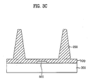
- Referring thirdly to FIG. 3C, the barrier rib paste 700a over the light emitting cell region is etched to a predetermined depth, to form the lower
dielectric layer 700 andbarrier rib 200 simultaneously. - Here, the barrier rib paste 700a may be etched by use of sand blasting, direct etching and photolithography methods, etc., to etch the light emitting cell region.
- Preferably, the etching depth of the barrier rib paste 700a is in the range of approximately 110 µm to 140 µm.
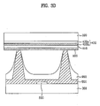
- Referring finally to FIG. 3D, after forming the
phosphors 900 on the side surfaces of thebarrier rib 200 and the upper surface of the lowerdielectric layer 700, theupper substrate 100, on which the pair of sustainelectrodes 400,upper dielectric layer 600 andprotective film 800 are formed in this sequence, is bonded onto thebarrier rib 200, completing the manufacture of the plasma display panel. - As apparent from the above description, the plasma display panel according to the present invention has the following effects.
- Firstly, as a result of eliminating a process for forming a dielectric layer on a lower substrate, the present invention can achieve a simplified overall process and reduced manufacturing costs.
- Secondly, by virtue of the fact that the present invention is free from many problems caused by the process for forming a dielectric layer on a lower substrate, the present invention can achieve the effects of improving optical efficiency and product quality.
- It will be apparent to those skilled in the art that various modifications and variations can be made in the present invention without departing from the spirit or scope of the inventions. Thus, it is intended that the present invention covers the modifications and variations of this invention provided they come within the scope of the appended claims and their equivalents.
Claims (20)
- A plasma display panel using a photosensitive barrier rib, wherein
the photosensitive barrier rib contains nano-powder. - The panel according to claim 1, wherein the photosensitive barrier rib contains a mixture of glass powder and nano-powder.
- The panel according to claim 1, wherein the nano-powder is any one of TiO2 and ZrO2.
- The panel according to claim 1, wherein the photosensitive barrier rib has a composition including 95-55% glass powder and 5-45% nano-powder.
- A plasma display panel having a plurality of light emitting cells between an upper substrate and a lower substrate comprising:address electrodes formed on the lower substrate and made of conductive material containing nano-powder;a dielectric layer formed over the entire surface of the lower substrate including the address electrodes; andbarrier ribs formed on the dielectric layer.
- The panel according to claim 5, wherein the nano-powder contained in the electrodes is at least one of Ni, Pd, Cu and Au.
- The panel according to claim 5, wherein the electrodes are made of Ag, metal-coated Ag, or any one or combinations of conductive metals.
- The panel according to claim 7, wherein the metal coated on Ag is nano-powder containing at least one of Ni, Pd, Cu and Au.
- A plasma display panel having a plurality of light emitting cells between an upper substrate and a lower substrate comprising:electrodes formed on the lower substrate;a dielectric layer formed over the entire surface of the lower substrate including the electrodes and containing nano-powder; andbarrier ribs formed on the dielectric layer and containing nano-powder.
- The panel according to claim 9, wherein the nano-powder contained in the dielectric layer and barrier rib is any one of TiO2 and ZrO2.
- The panel according to claim 9, wherein the dielectric layer and barrier rib have a composition including 95-55% glass powder and 5-45% nano-powder.
- A plasma display panel having a plurality of light emitting cells between an upper substrate and a lower substrate comprising:address electrodes formed on the lower substrate;a dielectric layer formed over the entire surface of the lower substrate including the address electrodes; andbarrier ribs formed on the dielectric layer and made of the same material as that of the dielectric layer.
- The panel according to claim 12, wherein the dielectric layer and barrier rib contain a mixture of glass powder and nano-powder.
- The panel according to claim 13, wherein the nano-powder is any one of TiO2 and ZrO2.
- The panel according to claim 13, wherein the dielectric layer and barrier rib have a composition including 95-55% glass powder and 5-45% nano-powder.
- A method of manufacturing a plasma display panel comprising:preparing upper and lower substrates having a light emitting cell region;forming electrodes on the upper and lower substrates, respectively, over the light emitting cell region;forming a barrier rib paste on the lower substrate including the electrode and firing the barrier rib paste;etching the barrier rib paste over the light emitting cell region to a predetermined depth, to form a dielectric layer and barrier rib simultaneously;forming phosphors on side surfaces of the barrier rib and on the dielectric layer over the light emitting cell region; andbonding the upper substrate onto the barrier rib.
- The method according to claim 13, wherein, in the preparation of the lower substrate, at least one surface of the lower substrate, namely, front and/or rear surface of the lower substrate, is subjected to a surface treatment, to achieve a desired reflectivity.
- The method according to claim 16, wherein the barrier rib paste is formed by mixing nano-powder into glass powder and organic solvent.
- The method according to claim 16, wherein a firing temperature of the barrier rib paste is in the range of 550°C to 600°C.
- The method according to claim 16, wherein, in the etching of the barrier rib paste, the predetermined etching depth is in the range of 110 µm to 140 µm.
Priority Applications (1)
| Application Number | Priority Date | Filing Date | Title |
|---|---|---|---|
| EP07016817A EP1879210A3 (en) | 2005-07-01 | 2006-06-30 | Plasma display panel and method of manufacturing the same |
Applications Claiming Priority (1)
| Application Number | Priority Date | Filing Date | Title |
|---|---|---|---|
| KR1020050059192A KR100763389B1 (en) | 2005-07-01 | 2005-07-01 | Plasma Display Panel And Method Of Manufacturing The Same |
Related Child Applications (1)
| Application Number | Title | Priority Date | Filing Date |
|---|---|---|---|
| EP07016817A Division EP1879210A3 (en) | 2005-07-01 | 2006-06-30 | Plasma display panel and method of manufacturing the same |
Publications (2)
| Publication Number | Publication Date |
|---|---|
| EP1742246A2 true EP1742246A2 (en) | 2007-01-10 |
| EP1742246A3 EP1742246A3 (en) | 2007-04-18 |
Family
ID=37394965
Family Applications (2)
| Application Number | Title | Priority Date | Filing Date |
|---|---|---|---|
| EP06253443A Withdrawn EP1742246A3 (en) | 2005-07-01 | 2006-06-30 | Plasma display panel and method of manufacturing the same |
| EP07016817A Withdrawn EP1879210A3 (en) | 2005-07-01 | 2006-06-30 | Plasma display panel and method of manufacturing the same |
Family Applications After (1)
| Application Number | Title | Priority Date | Filing Date |
|---|---|---|---|
| EP07016817A Withdrawn EP1879210A3 (en) | 2005-07-01 | 2006-06-30 | Plasma display panel and method of manufacturing the same |
Country Status (4)
| Country | Link |
|---|---|
| US (1) | US20070013310A1 (en) |
| EP (2) | EP1742246A3 (en) |
| JP (1) | JP2007012622A (en) |
| KR (1) | KR100763389B1 (en) |
Families Citing this family (1)
| Publication number | Priority date | Publication date | Assignee | Title |
|---|---|---|---|---|
| JP5239704B2 (en) * | 2008-09-30 | 2013-07-17 | 東レ株式会社 | Manufacturing method of member for display. |
Family Cites Families (9)
| Publication number | Priority date | Publication date | Assignee | Title |
|---|---|---|---|---|
| US5723945A (en) * | 1996-04-09 | 1998-03-03 | Electro Plasma, Inc. | Flat-panel display |
| KR100326558B1 (en) * | 1998-09-01 | 2002-09-17 | 엘지전자주식회사 | Composition of Barrier Rib for Plasma Display Panel |
| WO2000048218A1 (en) * | 1999-02-12 | 2000-08-17 | Toppan Printing Co., Ltd. | Plasma display panel, method and device for production therefor |
| US6731667B1 (en) * | 1999-11-18 | 2004-05-04 | Anapass Inc. | Zero-delay buffer circuit for a spread spectrum clock system and method therefor |
| JP3699336B2 (en) * | 2000-06-08 | 2005-09-28 | スリーエム イノベイティブ プロパティズ カンパニー | Manufacturing method of rib for plasma display panel substrate |
| WO2002035555A1 (en) * | 2000-10-23 | 2002-05-02 | Sekisui Chemical Co., Ltd. | Coated particle |
| JP4073201B2 (en) * | 2001-11-09 | 2008-04-09 | 株式会社日立製作所 | Plasma display panel and image display device including the same |
| KR100497763B1 (en) * | 2002-08-02 | 2005-08-03 | 일동화학 주식회사 | Photosensitive barrier rib paste composite having surface treated barrier rib powder with fumed silica particles, fabrication method thereof and method of forming barrier rib for plasma display panel using the same |
| US7431627B2 (en) * | 2003-12-12 | 2008-10-07 | Pioneer Corporation | Method of manufacturing plasma display panel and method of manufacturing plasma display apparatus |
-
2005
- 2005-07-01 KR KR1020050059192A patent/KR100763389B1/en not_active Expired - Fee Related
-
2006
- 2006-06-30 US US11/478,325 patent/US20070013310A1/en not_active Abandoned
- 2006-06-30 EP EP06253443A patent/EP1742246A3/en not_active Withdrawn
- 2006-06-30 EP EP07016817A patent/EP1879210A3/en not_active Withdrawn
- 2006-07-03 JP JP2006183092A patent/JP2007012622A/en not_active Withdrawn
Also Published As
| Publication number | Publication date |
|---|---|
| KR20070003310A (en) | 2007-01-05 |
| KR100763389B1 (en) | 2007-10-05 |
| JP2007012622A (en) | 2007-01-18 |
| EP1879210A2 (en) | 2008-01-16 |
| US20070013310A1 (en) | 2007-01-18 |
| EP1879210A3 (en) | 2008-01-23 |
| EP1742246A3 (en) | 2007-04-18 |
Similar Documents
| Publication | Publication Date | Title |
|---|---|---|
| JP4960617B2 (en) | Electromagnetic wave shielding filter, manufacturing method thereof, and plasma display panel device | |
| CN1253913C (en) | Electron emission thin film, plasma display panel comprising it and method of manufacturing them | |
| KR100285760B1 (en) | Bulkhead manufacturing method for plasma display panel and plasma display panel device using same | |
| CN1473093A (en) | Method for forming fine partition wall, method for producing flat display device, and abrasive material for blasting | |
| EP1742246A2 (en) | Plasma display panel and method of manufacturing the same | |
| US6712663B2 (en) | Method of manufacturing plasma-display-panel-substrate, plasma-display-panel-substrate, and plasma display panel | |
| JP3067673B2 (en) | Color plasma display panel | |
| CN1545715A (en) | Method for manufacturing plasma display panel | |
| CN101150031A (en) | Plasma display panel and method of forming barrier ribs of plasma display panel | |
| US7482748B2 (en) | Plasma display panel with paste composite for white-black formation | |
| JP3299707B2 (en) | Method for manufacturing plasma display panel | |
| KR20090021733A (en) | Plasma Display Panel And Method Of Manufacturing The Same | |
| EP1367621A1 (en) | Plasma display panel and method for manufacture thereof | |
| KR100813037B1 (en) | Plasma Display Panel And Method Of Manufacturing The Same | |
| KR100710360B1 (en) | Plasma display panel | |
| CN1805097A (en) | Plasma display panel and manufacturing method of the same | |
| EP1677333A1 (en) | Green sheet, plasma display panel and method for manufacturing plasma display panel | |
| JP2002033054A (en) | Electron-emitting thin film, plasma display panel using the same, and manufacturing method thereof | |
| KR100593071B1 (en) | Plasma Display Panel And Method Of Manufacturing The Same | |
| US20080297049A1 (en) | Plasma display panel and method for fabricating the same | |
| JP2001319569A (en) | Method for manufacturing plasma display panel substrate, plasma display panel substrate, and plasma display panel | |
| JP2002313241A (en) | Plasma display panel and method of manufacturing the same | |
| US7768205B2 (en) | Plasma display panel and method of manufacturing the same | |
| US20060138955A1 (en) | Plasma display panel and manufacturing method thereof | |
| KR100496255B1 (en) | Plasma Display Panel and Method of Fabricating The same |
Legal Events
| Date | Code | Title | Description |
|---|---|---|---|
| PUAI | Public reference made under article 153(3) epc to a published international application that has entered the european phase |
Free format text: ORIGINAL CODE: 0009012 |
|
| AK | Designated contracting states |
Kind code of ref document: A2 Designated state(s): AT BE BG CH CY CZ DE DK EE ES FI FR GB GR HU IE IS IT LI LT LU LV MC NL PL PT RO SE SI SK TR |
|
| AX | Request for extension of the european patent |
Extension state: AL BA HR MK YU |
|
| PUAL | Search report despatched |
Free format text: ORIGINAL CODE: 0009013 |
|
| AK | Designated contracting states |
Kind code of ref document: A3 Designated state(s): AT BE BG CH CY CZ DE DK EE ES FI FR GB GR HU IE IS IT LI LT LU LV MC NL PL PT RO SE SI SK TR |
|
| AX | Request for extension of the european patent |
Extension state: AL BA HR MK YU |
|
| 17P | Request for examination filed |
Effective date: 20070821 |
|
| AKX | Designation fees paid |
Designated state(s): DE FR GB NL |
|
| STAA | Information on the status of an ep patent application or granted ep patent |
Free format text: STATUS: THE APPLICATION IS DEEMED TO BE WITHDRAWN |
|
| 18D | Application deemed to be withdrawn |
Effective date: 20100105 |