EP1736525A1 - Oxynitride phosphor and light-emitting device - Google Patents
Oxynitride phosphor and light-emitting device Download PDFInfo
- Publication number
- EP1736525A1 EP1736525A1 EP05726717A EP05726717A EP1736525A1 EP 1736525 A1 EP1736525 A1 EP 1736525A1 EP 05726717 A EP05726717 A EP 05726717A EP 05726717 A EP05726717 A EP 05726717A EP 1736525 A1 EP1736525 A1 EP 1736525A1
- Authority
- EP
- European Patent Office
- Prior art keywords
- light emitting
- emitting diode
- phosphor
- excitation
- composition
- Prior art date
- Legal status (The legal status is an assumption and is not a legal conclusion. Google has not performed a legal analysis and makes no representation as to the accuracy of the status listed.)
- Granted
Links
Images







Classifications
-
- C—CHEMISTRY; METALLURGY
- C09—DYES; PAINTS; POLISHES; NATURAL RESINS; ADHESIVES; COMPOSITIONS NOT OTHERWISE PROVIDED FOR; APPLICATIONS OF MATERIALS NOT OTHERWISE PROVIDED FOR
- C09K—MATERIALS FOR MISCELLANEOUS APPLICATIONS, NOT PROVIDED FOR ELSEWHERE
- C09K11/00—Luminescent materials, e.g. electroluminescent or chemiluminescent
- C09K11/08—Luminescent materials, e.g. electroluminescent or chemiluminescent containing inorganic luminescent materials
- C09K11/64—Luminescent materials, e.g. electroluminescent or chemiluminescent containing inorganic luminescent materials containing aluminium
-
- C—CHEMISTRY; METALLURGY
- C04—CEMENTS; CONCRETE; ARTIFICIAL STONE; CERAMICS; REFRACTORIES
- C04B—LIME, MAGNESIA; SLAG; CEMENTS; COMPOSITIONS THEREOF, e.g. MORTARS, CONCRETE OR LIKE BUILDING MATERIALS; ARTIFICIAL STONE; CERAMICS; REFRACTORIES; TREATMENT OF NATURAL STONE
- C04B35/00—Shaped ceramic products characterised by their composition; Ceramics compositions; Processing powders of inorganic compounds preparatory to the manufacturing of ceramic products
- C04B35/515—Shaped ceramic products characterised by their composition; Ceramics compositions; Processing powders of inorganic compounds preparatory to the manufacturing of ceramic products based on non-oxide ceramics
- C04B35/58—Shaped ceramic products characterised by their composition; Ceramics compositions; Processing powders of inorganic compounds preparatory to the manufacturing of ceramic products based on non-oxide ceramics based on borides, nitrides, i.e. nitrides, oxynitrides, carbonitrides or oxycarbonitrides or silicides
- C04B35/597—Shaped ceramic products characterised by their composition; Ceramics compositions; Processing powders of inorganic compounds preparatory to the manufacturing of ceramic products based on non-oxide ceramics based on borides, nitrides, i.e. nitrides, oxynitrides, carbonitrides or oxycarbonitrides or silicides based on silicon oxynitride, e.g. SIALONS
-
- C—CHEMISTRY; METALLURGY
- C09—DYES; PAINTS; POLISHES; NATURAL RESINS; ADHESIVES; COMPOSITIONS NOT OTHERWISE PROVIDED FOR; APPLICATIONS OF MATERIALS NOT OTHERWISE PROVIDED FOR
- C09K—MATERIALS FOR MISCELLANEOUS APPLICATIONS, NOT PROVIDED FOR ELSEWHERE
- C09K11/00—Luminescent materials, e.g. electroluminescent or chemiluminescent
- C09K11/08—Luminescent materials, e.g. electroluminescent or chemiluminescent containing inorganic luminescent materials
- C09K11/0883—Arsenides; Nitrides; Phosphides
-
- C—CHEMISTRY; METALLURGY
- C09—DYES; PAINTS; POLISHES; NATURAL RESINS; ADHESIVES; COMPOSITIONS NOT OTHERWISE PROVIDED FOR; APPLICATIONS OF MATERIALS NOT OTHERWISE PROVIDED FOR
- C09K—MATERIALS FOR MISCELLANEOUS APPLICATIONS, NOT PROVIDED FOR ELSEWHERE
- C09K11/00—Luminescent materials, e.g. electroluminescent or chemiluminescent
- C09K11/08—Luminescent materials, e.g. electroluminescent or chemiluminescent containing inorganic luminescent materials
- C09K11/55—Luminescent materials, e.g. electroluminescent or chemiluminescent containing inorganic luminescent materials containing beryllium, magnesium, alkali metals or alkaline earth metals
-
- C—CHEMISTRY; METALLURGY
- C09—DYES; PAINTS; POLISHES; NATURAL RESINS; ADHESIVES; COMPOSITIONS NOT OTHERWISE PROVIDED FOR; APPLICATIONS OF MATERIALS NOT OTHERWISE PROVIDED FOR
- C09K—MATERIALS FOR MISCELLANEOUS APPLICATIONS, NOT PROVIDED FOR ELSEWHERE
- C09K11/00—Luminescent materials, e.g. electroluminescent or chemiluminescent
- C09K11/08—Luminescent materials, e.g. electroluminescent or chemiluminescent containing inorganic luminescent materials
- C09K11/59—Luminescent materials, e.g. electroluminescent or chemiluminescent containing inorganic luminescent materials containing silicon
-
- C—CHEMISTRY; METALLURGY
- C09—DYES; PAINTS; POLISHES; NATURAL RESINS; ADHESIVES; COMPOSITIONS NOT OTHERWISE PROVIDED FOR; APPLICATIONS OF MATERIALS NOT OTHERWISE PROVIDED FOR
- C09K—MATERIALS FOR MISCELLANEOUS APPLICATIONS, NOT PROVIDED FOR ELSEWHERE
- C09K11/00—Luminescent materials, e.g. electroluminescent or chemiluminescent
- C09K11/08—Luminescent materials, e.g. electroluminescent or chemiluminescent containing inorganic luminescent materials
- C09K11/77—Luminescent materials, e.g. electroluminescent or chemiluminescent containing inorganic luminescent materials containing rare earth metals
- C09K11/7728—Luminescent materials, e.g. electroluminescent or chemiluminescent containing inorganic luminescent materials containing rare earth metals containing europium
- C09K11/77348—Silicon Aluminium Nitrides or Silicon Aluminium Oxynitrides
-
- H—ELECTRICITY
- H05—ELECTRIC TECHNIQUES NOT OTHERWISE PROVIDED FOR
- H05B—ELECTRIC HEATING; ELECTRIC LIGHT SOURCES NOT OTHERWISE PROVIDED FOR; CIRCUIT ARRANGEMENTS FOR ELECTRIC LIGHT SOURCES, IN GENERAL
- H05B33/00—Electroluminescent light sources
- H05B33/12—Light sources with substantially two-dimensional [2D] radiating surfaces
- H05B33/14—Light sources with substantially two-dimensional [2D] radiating surfaces characterised by the chemical or physical composition or the arrangement of the electroluminescent material, or by the simultaneous addition of the electroluminescent material in or onto the light source
-
- H—ELECTRICITY
- H10—SEMICONDUCTOR DEVICES; ELECTRIC SOLID-STATE DEVICES NOT OTHERWISE PROVIDED FOR
- H10H—INORGANIC LIGHT-EMITTING SEMICONDUCTOR DEVICES HAVING POTENTIAL BARRIERS
- H10H20/00—Individual inorganic light-emitting semiconductor devices having potential barriers, e.g. light-emitting diodes [LED]
- H10H20/80—Constructional details
- H10H20/85—Packages
- H10H20/851—Wavelength conversion means
- H10H20/8511—Wavelength conversion means characterised by their material, e.g. binder
- H10H20/8512—Wavelength conversion materials
-
- C—CHEMISTRY; METALLURGY
- C04—CEMENTS; CONCRETE; ARTIFICIAL STONE; CERAMICS; REFRACTORIES
- C04B—LIME, MAGNESIA; SLAG; CEMENTS; COMPOSITIONS THEREOF, e.g. MORTARS, CONCRETE OR LIKE BUILDING MATERIALS; ARTIFICIAL STONE; CERAMICS; REFRACTORIES; TREATMENT OF NATURAL STONE
- C04B2235/00—Aspects relating to ceramic starting mixtures or sintered ceramic products
- C04B2235/02—Composition of constituents of the starting material or of secondary phases of the final product
- C04B2235/30—Constituents and secondary phases not being of a fibrous nature
- C04B2235/32—Metal oxides, mixed metal oxides, or oxide-forming salts thereof, e.g. carbonates, nitrates, (oxy)hydroxides, chlorides
- C04B2235/3205—Alkaline earth oxides or oxide forming salts thereof, e.g. beryllium oxide
- C04B2235/3208—Calcium oxide or oxide-forming salts thereof, e.g. lime
-
- C—CHEMISTRY; METALLURGY
- C04—CEMENTS; CONCRETE; ARTIFICIAL STONE; CERAMICS; REFRACTORIES
- C04B—LIME, MAGNESIA; SLAG; CEMENTS; COMPOSITIONS THEREOF, e.g. MORTARS, CONCRETE OR LIKE BUILDING MATERIALS; ARTIFICIAL STONE; CERAMICS; REFRACTORIES; TREATMENT OF NATURAL STONE
- C04B2235/00—Aspects relating to ceramic starting mixtures or sintered ceramic products
- C04B2235/02—Composition of constituents of the starting material or of secondary phases of the final product
- C04B2235/30—Constituents and secondary phases not being of a fibrous nature
- C04B2235/32—Metal oxides, mixed metal oxides, or oxide-forming salts thereof, e.g. carbonates, nitrates, (oxy)hydroxides, chlorides
- C04B2235/3224—Rare earth oxide or oxide forming salts thereof, e.g. scandium oxide
-
- C—CHEMISTRY; METALLURGY
- C04—CEMENTS; CONCRETE; ARTIFICIAL STONE; CERAMICS; REFRACTORIES
- C04B—LIME, MAGNESIA; SLAG; CEMENTS; COMPOSITIONS THEREOF, e.g. MORTARS, CONCRETE OR LIKE BUILDING MATERIALS; ARTIFICIAL STONE; CERAMICS; REFRACTORIES; TREATMENT OF NATURAL STONE
- C04B2235/00—Aspects relating to ceramic starting mixtures or sintered ceramic products
- C04B2235/02—Composition of constituents of the starting material or of secondary phases of the final product
- C04B2235/30—Constituents and secondary phases not being of a fibrous nature
- C04B2235/38—Non-oxide ceramic constituents or additives
- C04B2235/3852—Nitrides, e.g. oxynitrides, carbonitrides, oxycarbonitrides, lithium nitride, magnesium nitride
- C04B2235/3865—Aluminium nitrides
-
- C—CHEMISTRY; METALLURGY
- C04—CEMENTS; CONCRETE; ARTIFICIAL STONE; CERAMICS; REFRACTORIES
- C04B—LIME, MAGNESIA; SLAG; CEMENTS; COMPOSITIONS THEREOF, e.g. MORTARS, CONCRETE OR LIKE BUILDING MATERIALS; ARTIFICIAL STONE; CERAMICS; REFRACTORIES; TREATMENT OF NATURAL STONE
- C04B2235/00—Aspects relating to ceramic starting mixtures or sintered ceramic products
- C04B2235/02—Composition of constituents of the starting material or of secondary phases of the final product
- C04B2235/30—Constituents and secondary phases not being of a fibrous nature
- C04B2235/38—Non-oxide ceramic constituents or additives
- C04B2235/3852—Nitrides, e.g. oxynitrides, carbonitrides, oxycarbonitrides, lithium nitride, magnesium nitride
- C04B2235/3873—Silicon nitrides, e.g. silicon carbonitride, silicon oxynitride
- C04B2235/3878—Alpha silicon nitrides
-
- C—CHEMISTRY; METALLURGY
- C04—CEMENTS; CONCRETE; ARTIFICIAL STONE; CERAMICS; REFRACTORIES
- C04B—LIME, MAGNESIA; SLAG; CEMENTS; COMPOSITIONS THEREOF, e.g. MORTARS, CONCRETE OR LIKE BUILDING MATERIALS; ARTIFICIAL STONE; CERAMICS; REFRACTORIES; TREATMENT OF NATURAL STONE
- C04B2235/00—Aspects relating to ceramic starting mixtures or sintered ceramic products
- C04B2235/02—Composition of constituents of the starting material or of secondary phases of the final product
- C04B2235/30—Constituents and secondary phases not being of a fibrous nature
- C04B2235/44—Metal salt constituents or additives chosen for the nature of the anions, e.g. hydrides or acetylacetonate
- C04B2235/442—Carbonates
-
- C—CHEMISTRY; METALLURGY
- C04—CEMENTS; CONCRETE; ARTIFICIAL STONE; CERAMICS; REFRACTORIES
- C04B—LIME, MAGNESIA; SLAG; CEMENTS; COMPOSITIONS THEREOF, e.g. MORTARS, CONCRETE OR LIKE BUILDING MATERIALS; ARTIFICIAL STONE; CERAMICS; REFRACTORIES; TREATMENT OF NATURAL STONE
- C04B2235/00—Aspects relating to ceramic starting mixtures or sintered ceramic products
- C04B2235/70—Aspects relating to sintered or melt-casted ceramic products
- C04B2235/74—Physical characteristics
- C04B2235/76—Crystal structural characteristics, e.g. symmetry
- C04B2235/766—Trigonal symmetry, e.g. alpha-Si3N4 or alpha-Sialon
-
- H—ELECTRICITY
- H10—SEMICONDUCTOR DEVICES; ELECTRIC SOLID-STATE DEVICES NOT OTHERWISE PROVIDED FOR
- H10W—GENERIC PACKAGES, INTERCONNECTIONS, CONNECTORS OR OTHER CONSTRUCTIONAL DETAILS OF DEVICES COVERED BY CLASS H10
- H10W72/00—Interconnections or connectors in packages
- H10W72/01—Manufacture or treatment
- H10W72/015—Manufacture or treatment of bond wires
- H10W72/01515—Forming coatings
-
- H—ELECTRICITY
- H10—SEMICONDUCTOR DEVICES; ELECTRIC SOLID-STATE DEVICES NOT OTHERWISE PROVIDED FOR
- H10W—GENERIC PACKAGES, INTERCONNECTIONS, CONNECTORS OR OTHER CONSTRUCTIONAL DETAILS OF DEVICES COVERED BY CLASS H10
- H10W72/00—Interconnections or connectors in packages
- H10W72/071—Connecting or disconnecting
- H10W72/075—Connecting or disconnecting of bond wires
-
- H—ELECTRICITY
- H10—SEMICONDUCTOR DEVICES; ELECTRIC SOLID-STATE DEVICES NOT OTHERWISE PROVIDED FOR
- H10W—GENERIC PACKAGES, INTERCONNECTIONS, CONNECTORS OR OTHER CONSTRUCTIONAL DETAILS OF DEVICES COVERED BY CLASS H10
- H10W74/00—Encapsulations, e.g. protective coatings
-
- H—ELECTRICITY
- H10—SEMICONDUCTOR DEVICES; ELECTRIC SOLID-STATE DEVICES NOT OTHERWISE PROVIDED FOR
- H10W—GENERIC PACKAGES, INTERCONNECTIONS, CONNECTORS OR OTHER CONSTRUCTIONAL DETAILS OF DEVICES COVERED BY CLASS H10
- H10W90/00—Package configurations
- H10W90/701—Package configurations characterised by the relative positions of pads or connectors relative to package parts
- H10W90/751—Package configurations characterised by the relative positions of pads or connectors relative to package parts of bond wires
- H10W90/756—Package configurations characterised by the relative positions of pads or connectors relative to package parts of bond wires between a chip and a stacked lead frame, conducting package substrate or heat sink
-
- Y—GENERAL TAGGING OF NEW TECHNOLOGICAL DEVELOPMENTS; GENERAL TAGGING OF CROSS-SECTIONAL TECHNOLOGIES SPANNING OVER SEVERAL SECTIONS OF THE IPC; TECHNICAL SUBJECTS COVERED BY FORMER USPC CROSS-REFERENCE ART COLLECTIONS [XRACs] AND DIGESTS
- Y02—TECHNOLOGIES OR APPLICATIONS FOR MITIGATION OR ADAPTATION AGAINST CLIMATE CHANGE
- Y02B—CLIMATE CHANGE MITIGATION TECHNOLOGIES RELATED TO BUILDINGS, e.g. HOUSING, HOUSE APPLIANCES OR RELATED END-USER APPLICATIONS
- Y02B20/00—Energy efficient lighting technologies, e.g. halogen lamps or gas discharge lamps
Definitions
- the present invention relates to a europium-activated oxynitride phosphor and a light emitting device using the same.
- a new phosphor such as a nitride or oxynitride phosphor has attracted a lot of attention and inspired vigorous researches in recent years.
- the Ca-alpha-SiAlON phosphor is referred to simply as SiAlON phosphor, when appropriate, hereinafter.
- the SiAlON phosphor can be used for example as a wavelength conversion material for a white light emitting diode (white LED) equipped with a blue light emitting diode chip (blue LED) as an excitation light source.
- white LED white light emitting diode
- blue LED blue light emitting diode chip
- the above white light emitting diode has drawn attention as a next-generation highly efficient lighting apparatus substituting a conventional incandescent or fluorescent lamp and attracted active investigations on such a diode.
- the mainstream white light emitting diode is configured to have a blue light emitting diode chip as an excitation light source and a phosphor for converting a wavelength of part of blue light emitted from the blue light emitting diode chip into a different wavelength, thereby emitting white light as a result of color mixture of blue light from the blue light emitting diode chip and the wavelength-converted yellow-light.
- SiAlON phosphor is suitable as a wavelength conversion material for the white light emitting diode of such a type, a further improvement in luminous efficacy and intensity have been desired.
- a first aspect of the present invention provides an oxynitride phosphor represented by a general formula Ca x (Si, Al) 12 (O, N) 16 :Eu 2+ y , wherein a Ca composition of x is in a range of from 0.75 to 1.0 and a Eu composition of y is in a range of from 0.04 to 0.25, and wherein a main phase thereof has substantially an alpha-SiAlON crystal structure.
- a second aspect of the present invention provides a light emitting device comprising a semiconductor light source element and a wavelength conversion material that converts a wavelength of light emitted from the semiconductor light source element, wherein the wavelength conversion material is represented by a general formula Ca x (Si, Al) 12 (O, N) 16 :Eu 2+ y , in which a Ca composition of x is in a range of from 0.75 to 1.0 and a Eu composition of y is in a range of from 0.04 to 0.25, and in which a main phase thereof has substantially an alpha SiAlON crystal structure.
- a third aspect of the present invention provides a light emitting device according to the second aspect, wherein the semiconductor light source element is a semiconductor light emitting diode element that has a primary emission wavelength in a range of from 400 nm to 480 nm.
- a divalent-europium activated Ca-alpha-SiAlON having a composition that falls within a certain range has an exceptionally higher luminous intensity than those having the other compositions.
- the alpha-SiAlON phosphor is a divalent-europium activated Ca-alpha-SiAlON phosphor having the following chemical formula (1) or (2): Ca x Si 12-(m+n) Al (m+n) O n N 16-n :Eu 2+ y (1) Ca x (Si, Al) 12 (O, N) 16 : Eu 2+ y (2)
- alpha Silicon Nitride Si 3 N 4
- Aluminum Nitride AlN
- Calcium Carbonate CaCO 3
- Europium Oxide Eu 2 O 3
- the starting materials in powder form were weighed in accordance with the designed composition stated above and mixed. Prior to mixing, a predetermined amount of n-hexane was added to the weighed materials and then the n-hexane-added materials were well mixed by a planetary ball mill for 2 hours.
- the mixed materials were desiccated by a rotary evaporator and then pounded well in a mortar. Next, the pounded materials were charged into a covered container made of Boron Nitride.
- the sintering process was carried out for the powder materials in the covered container at a temperature of 1,600 degrees Celsius in a 0.1 MPa Nitrogen atmosphere for about 8 hours.
- the measurement was carried out by a fluorescence spectrophotometer, which spectral distribution was corrected using Rhodamine B and a standard light source.
- FIG. 3 illustrates an excitation spectrum (line A) and an emission spectrum (line B) of the sample #3. These spectra have been measured by the fluorescence spectrophotometer.
- the emission monitoring wavelength when measuring the excitation spectrum was 582 nm and the excitation wavelength when measuring the emission spectrum was 410 nm, as is the case with FIG. 2.
- the SiAlON phosphor according to the present invention including the sample #3 is preferable for use in a light emitting device applicable to various light emitting apparatuses or display apparatuses.
- theSiAlON phosphor according to the present invention is suitable as a wavelength conversion material for use in a white light emitting diode lamp for general illumination.
- the white light emitting diode lamp is categorized into a near-ultraviolet excitation type and a blue excitation type. The latter will be described hereinafter as an embodiment of the white light emitting diode lamp, the type being now in a mainstream of a white light emitting diode lamp.
- the white light emitting diode lamp of blue excitation type has a semiconductor blue light emitting diode chip and a phosphor that is excited by the blue light emitted from the diode chip and emanates yellow light, which is a complementary color of blue.
- FIG. 4 summarizes the dominant wavelengths in emission spectra of the phosphors having a higher luminous intensity among the samples listed in FIG. 2, the emission spectra being measured with excitation wavelengths of 450 nm, 460 nm, and 470 nm, respectively.
- lines C, D, and E represent the emission spectra of the samples 2, 3, and 4, respectively.
- lines F, G, and H represent the emission spectra of the samples 3, 8, and 13, respectively.
- the SiAlON phosphor according to the present invention is preferable for a blue-excitation-type white light emitting diode (a white light emitting diode lamp for general illumination).
- the SiAlON phosphor according to the present invention can be efficiently excited by near-ultraviolet light as well, the phosphor is preferably used as a yellow phosphor for a near-ultraviolet-excitation-type white light emitting diode lamp when it is mixed with another phosphors.
- a white light emitting diode lamp will be described as an embodiment of a light emitting device comprised of the SiAlON phosphor according to the present invention.
- FIG. 7 is a cross-sectional view of a light emitting diode lamp 1a according to a first embodiment (embodiment 1) of the present invention.
- FIG. 8 is a perspective view of the light emitting diode lamp 1a illustrated in FIG. 7.
- the light emitting diode lamp 1a is formed into a tubular shape with a round end at its top, in other words, a shape resembling an artillery shell.
- the light emitting diode lamp 1a includes lead wires 2, 3, a light emitting diode chip (blue light emitting diode chip) 4, a bonding wire 5, a phosphor (wavelength conversion material) 7, a first resin 6, and a second resin 8. The lower portion of the lead wires 2, 3 is exposed out of the second resin 8.
- a cup At the upper end of the lead wire 2, there is provided a cup in which a light emitting diode chip 4 (light emitting element) is placed.
- the light emitting diode chip 4 is electrically connected with the lead wire 2 by die bonding or the like using electrically conductive paste.
- the light emitting diode chip 4 is also electrically connected with the lead wire 3 by wire bonding or the like using the bonding wire 5.
- the vicinities of the light emitting diode chip 4, including the recess of the above-stated cup, are sealed with the first resin 6 into which the phosphor 7 is dispersed.
- the lead wires 2, 3, the light emitting diode chip 4, the bonding wire 5, and the first resin 6 are sealed with the second resin 8.
- the light emitting diode chip 4 is die-bonded in the cup at the tip of the lead wire 2 with electrically conductive paste.
- the light emitting diode chip 4 is wire-bonded to the lead wire 3 with the bonding wire 5.
- the first resin 6 dispersed adequately with the SiAlON phosphor 7 is pre-deposited onto the element-accommodating cup to coat the light emitting diode chip 4 and then cured.
- the second resin 8 is deposited to enfold the lead wires 2, 3, the light emitting diode chip 4 and the first resin 6 and then cured.
- the fourth process is ordinarily carried out by casting.
- the lead wires 2, 3 can be made as an integral member in which both of the wires are connected at their ends.
- a fifth process has to be adopted after the fourth process, wherein the connecting portion between the lead wires is removed to separate the lead wires 2, 3 into an individual member.
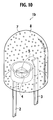
- FIGS. 9 and 10 are respectively a cross-sectional and a perspective view of the white light emitting diode lamp 1b according to the second embodiment.
- the SiAlON phosphor 7 is dispersed in the vicinities of the light emitting diode chip 4, in other words, in the first resin 6, the white light emitting device lamp according to the present invention is not limited to this structure.
- the SiAlON phosphor 7 can be dispersed in the second resin 8 as illustrated in the second embodiment.
- the second resin 8 dispersed with the phosphor is deposited and cured.
- An operational effect exerted by the white light emitting diode lamp 1b is the same as that by the white light emitting diode lamp 1a.
- the blue light emitting diode chip 4 can emit light in a wavelength range of from 400 nm to 480 nm.
- the lamp in case of a white light emitting diode lamp of ultraviolet excitation type, can be comprised of a ultraviolet light emitting diode chip and a mixture of two to five kinds of powder phosphors, one of which is the SiAlON phosphor (for example, the sample #3) according to the present invention.
- a white light emitting diode lamp which emits light having a low color temperature and allows anyone to readily recognize a warm nuance when he or she sees the diode emit white light.
- the emission intensity thereof is greater than that of a white light emitting diode lamp using a conventional alpha-SiAlON phosphor.
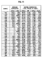
- FIG. 11 summarizes designed compositions of each sample used in the second experiment and mixture compositions of each source material calculated in accordance with the designed compositions. As apparent when compared with the sample listed in FIG.1, twenty-three out of 28 samples have the same compositions as those in FIG. 1.
- the mixed materials were desiccated by a rotary evaporator and then pounded well in a mortar.
- the pounded materials were granulated using a stainless steel test sieve having an aperture size of 125 micrometers to obtain powdered materials having a corresponding grain diameter, which were then charged into a covered container made of Boron Nitride.
- the excitation and emission spectra of the 28 powder phosphor samples were measured.
- the measurement was carried out by a fluorescence spectrophotometer, which spectral distribution was corrected using Rhodamine B and a standard light source.
- FIG. 12 summarizes fluorescent intensities and emission peak wavelengths obtained from the measurement with excitation wavelengths of 450 nm and 405 nm, respectively.
- the excitation wavelength of 450 nm was employed on the assumption that the phosphor samples in this embodiment are applied to a white light emitting diode lamp of blue excitation type, which now stays in a mainstream, whereas the excitation wavelength of 405 nm was employed on the assumption that the samples are applied to a white light emitting diode lamp of near-ultraviolet excitation type, which is prospected to come into a wide use.
- a white light emitting diode lamp of 405 nm excitation type is also referred to as near-ultraviolet excitation type or purplish-blue excitation type.
- the samples #38, #42, #43, #33, #37, #32, and #47 have extremely high fluorescent intensities, while the samples #48, #41, #52, #34, #39 and #44 have sufficiently high fluorescent intensities. From the results, it is found that excellent characteristics have been obtained from a sample having a value of x from 0.75 to 1.0 and a value of y from 0.04 to 0.25. These results are substantially the same as those in the first experiment.
- the SiAlON phosphor has more excellent characteristics.
- the phosphor quality may be improved by increasing the sintering temperature and the nitrogen pressure.
- a phosphor having a large value of x is not easily sintered and thereby a higher temperature and pressure probably be required compared with a sample having a relatively small value of x.
- a lower sinter temperature and a lower nitrogen pressure are preferable in terms of fabrication costs and also a prevention of quality degradation caused by deviations in production conditions.
- a phosphor having a value of x from 0.75 to 1.0 and a value of y from 0.04 to 0.25 is preferable.
- the phosphor has a value of x from 0.75 to 1.0 and a value of y from 0.04 to 0.0833.
- FIG. 13 illustrates the excitation and emission spectra of the phosphor sample according to this embodiment (denoted as FY6 hereinafter) and a commercially available yttrium-aluminum-garnet phosphor.
- the sample FY6 has a composition x and y of 0.875 and 0.07, respectively.
- a mixture composition of starting materials for FY6 was 65.14 wt % of alpha-Si 3 N 4 , 19.03 wt % of AlN, 13.56 wt % of CaCO 3 , and 2.27 wt % of Eu 2 O 3 .
- sintering process was carried out at a temperature of 1,700 degrees Celsius under nitrogen atmosphere of 0.5 MPa for 50 hours. After sintering, the sintered materials were classified using a stainless steel test sieve having an aperture size of 45 micrometers to obtain powdered materials having a grain diameter of 45 micrometers or smaller. Except the above conditions, the sample was prepared in accordance with the procedures described in the embodiment 3.
- a phosphor for comparison has a composition represented generally by (Y, Gd) 3 Al 5 O 12 :Ce 3+ .
- An emission spectrum of the sample FY6 was measured using an excitation light having a wavelength of 450 nm. Also, an excitation spectrum of the sample FY6 was measured using an emission monitoring wavelength of 585 nm. On the other hand, regarding a commercially available yttrium-aluminum-garnet phosphor, an excitation spectrum was measured with an excitation wavelength of 460 nm and an emission spectrum was measured with an emission monitoring wavelength of 568 nm. The measurements were carried out by a fluorescence spectrophotometer, which spectral distribution was corrected using Rhodamine B and a standard light source.
- lines I and J represent the excitation and emission spectra of the sample FY6, respectively, whereas lines K and L represent the excitation and emission spectra of the yttrium-aluminum-garnet, respectively.
- the sample FY6 has a far higher fluorescent intensity compared with the yttrium-aluminum-garnet.
- the sample FY6 has a higher excitation intensity and a very wide width covering an ultraviolet to blue region of the spectrum compared with the commercially available yttrium-aluminum-garnet.
- the light emitting diode lamp according to the embodiment 5 is a light emitting diode lamp of artillery shell type as shown in FIGS. 7 and 8.
- a phosphor 7 is used the sample FY6 stated above in the embodiment 4.
- a blue light emitting diode chip 4 is used an InGaN blue light emitting diode chip fabricated on a SiC substrate. The emission peak wavelength of the InGaN blue light emitting diode chip is measured to be about 454 nm.
- the light emitting diode lamp according to the embodiment 5 has a luminous efficacy of 36.3 lm/W, a color temperature of 2780 K, and CIE1931 chromaticity coordinates (x, y) of (0.46, 0.41). From these measurements, the light emitting diode lamp has a chromaticity corresponding to the incandescent lamp color which is defined along with the daylight color, the daylight-white color, the cool-white color, and the warm-white color in Japanese Industrial Standard (JIS) Z 9112-1990 "Classification of fluorescent lamps by chromaticity and color rendering property".
- JIS Japanese Industrial Standard
- a light emitting diode lamp having a chromaticity of an incandescent lamp color is chosen from various types of commercially available light emitting diode lamps of artillery shell type.
- This commercially available light emitting diode lamp for comparison has a luminous efficacy of 22.5 lm/W, a color temperature of 2,800 K, and CIE1931 chromaticity coordinates (x, y) of (0.46, 0.41).
- FIG. 14 illustrates the comparison result, in which lines M and N are emission spectra of the light emitting diode lamp according to the embodiment 5 and the commercially available light emitting diode lamp, respectively.
- the light emitting diode lamp according to the embodiment 5 has a higher emission intensity compared with the commercially available light emitting diode lamp.
- the luminous efficacy of the light emitting diode lamp according to the embodiment 5 is 1.6 times as high as the commercially available one.
- an oxynitride phosphor and a light emitting device have been described.
- the present invention is not limited to the embodiments and various modifications thereof are possible.
- the first and second embodiments have described in detail the light emitting diode chip 4 having one electrode on an upper side (i.e., on the side to be connected with the bonding wire 5) and the other on a lower side (i.e., on the side to contact with the element-accommodating cup)
- a light emitting diode chip having two electrodes on the upper side and none on the lower side can be used.
- an electrically conductive paste is not necessarily required in the first process. Instead, two bonding wires are used for bonding in the second process.
- lead wires is not limited to that illustrated here as far as the light emitting diode chip can be placed thereon.
- luminous efficacy and intensity can be improved, thereby providing a next-generation lighting apparatus that will substitute a conventional incandescent lamp or a fluorescent lamp.
Landscapes
- Chemical & Material Sciences (AREA)
- Engineering & Computer Science (AREA)
- Materials Engineering (AREA)
- Organic Chemistry (AREA)
- Inorganic Chemistry (AREA)
- Ceramic Engineering (AREA)
- Manufacturing & Machinery (AREA)
- Structural Engineering (AREA)
- Luminescent Compositions (AREA)
- Led Device Packages (AREA)
Abstract
Description
- The present invention relates to a europium-activated oxynitride phosphor and a light emitting device using the same.
- While it is an oxide or sulfide that has since been used as a phosphor, a new phosphor such as a nitride or oxynitride phosphor has attracted a lot of attention and inspired vigorous researches in recent years.
- Among the oxynitride phosphors that have been conventionally used, there is a divalent-activated Ca-alpha-SiAlON phosphor (See
Japanese Patent Application Laid-open Publication No. 2002-363554 - The SiAlON phosphor can be used for example as a wavelength conversion material for a white light emitting diode (white LED) equipped with a blue light emitting diode chip (blue LED) as an excitation light source.
- The above white light emitting diode has drawn attention as a next-generation highly efficient lighting apparatus substituting a conventional incandescent or fluorescent lamp and attracted active investigations on such a diode.
- Among several types of white light emitting diodes developed to date, the mainstream white light emitting diode is configured to have a blue light emitting diode chip as an excitation light source and a phosphor for converting a wavelength of part of blue light emitted from the blue light emitting diode chip into a different wavelength, thereby emitting white light as a result of color mixture of blue light from the blue light emitting diode chip and the wavelength-converted yellow-light.
- In order to improve luminous efficacy and intensity in a light emitting device including such a white light emitting diode of wavelength conversion type, there has to be improved not only the blue light emitting diode chip as an excitation light source but also a conversion efficiency of the phosphor.
- While the SiAlON phosphor is suitable as a wavelength conversion material for the white light emitting diode of such a type, a further improvement in luminous efficacy and intensity have been desired.
- A first aspect of the present invention provides an oxynitride phosphor represented by a general formula Cax(Si, Al)12(O, N)16:Eu2+ y, wherein a Ca composition of x is in a range of from 0.75 to 1.0 and a Eu composition of y is in a range of from 0.04 to 0.25, and wherein a main phase thereof has substantially an alpha-SiAlON crystal structure.
- A second aspect of the present invention provides a light emitting device comprising a semiconductor light source element and a wavelength conversion material that converts a wavelength of light emitted from the semiconductor light source element, wherein the wavelength conversion material is represented by a general formula Cax(Si, Al)12(O, N)16:Eu2+ y, in which a Ca composition of x is in a range of from 0.75 to 1.0 and a Eu composition of y is in a range of from 0.04 to 0.25, and in which a main phase thereof has substantially an alpha SiAlON crystal structure.
- A third aspect of the present invention provides a light emitting device according to the second aspect, wherein the semiconductor light source element is a semiconductor light emitting diode element that has a primary emission wavelength in a range of from 400 nm to 480 nm.
-
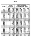
- FIG. 1 is a table listing compositions of each Eu-activated Ca-alpha-SiAlON sample.
- FIG. 2 is a table listing emission and excitation peak wavelengths and emission intensities.
- FIG. 3 illustrates excitation and emission spectra of a
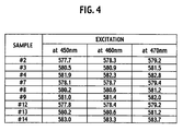
sample # 3. - FIG. 4 summarizes dominant wavelengths in emission spectra of the phosphors having a higher luminous intensity among the samples listed in FIG. 2, the emission spectra being measured with excitation wavelengths of 450 nm, 460 nm, and 470 nm, respectively.
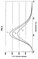
- FIG. 5 illustrates emission spectra of some of the samples having a value (Ca composition) of x=0.875, the emission spectra being measured with an excitation wavelength of 460 nm.
- FIG. 6 illustrates emission spectra of some of the samples having a value (Eu composition) of y=0.0833.
- FIG. 7 is a cross-sectional view of a white light
emitting diode lamp 1a according to a first embodiment of the present invention. - FIG. 8 is a perspective view of the white light emitting diode lamp illustrated in FIG. 7.
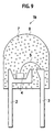
- FIG. 9 is a cross-sectional view of a white light
emitting diode lamp 1b according to a second embodiment. - FIG. 10 is a perspective view of the white light
emitting diode lamp 1b illustrated in FIG. 9. - FIG. 11 is a table listing compositions of each Eu-activated Ca-alpha-SiAlON sample used in the second experiment.
- FIG. 12 is a table listing fluorescent intensities and emission peak wavelengths of each sample listed in FIG. 11.
- FIG. 13 illustrates excitation and emission spectra of a phosphor sample according to a fourth embodiment and a commercially available yttrium-aluminum-garnet phosphor.
- FIG. 14 illustrates emission spectra of a light emitting diode lamp according to a fifth embodiment and a commercially available light emitting diode lamp for comparison.
- Referring to accompanying drawings, an oxynitride phosphor and a light emitting device according to the present invention will be described in detail.
- While a white light emitting diode lamp for general illumination will be described as an embodiment of the light emitting device according to the present invention in the following embodiments, they are intended for purposes of illustration only and are not intended to limit the scope of the invention. Therefore, whereas those skilled in the art can devise various types of alternatives, variations and modifications including each and all elements, all the alternatives, variations and modifications fall within the scope of the present invention.
- In addition, in all the drawings used as an aid in describing the following embodiments, identical reference numbers will be used to designate identical or corresponding elements, thereby eliminating unnecessary repetition of description about the identical elements.
- First of all, a SiAlON phosphor according to the present invention will be described hereinafter.
- After tenacious investigations performed to overcome the above-stated disadvantages, the inventors of the present invention have come to find that a divalent-europium activated Ca-alpha-SiAlON having a composition that falls within a certain range has an exceptionally higher luminous intensity than those having the other compositions.
- The alpha-SiAlON phosphor is a divalent-europium activated Ca-alpha-SiAlON phosphor having the following chemical formula (1) or (2):
CaxSi12-(m+n)Al(m+n)OnN16-n:Eu2+ y (1)
Cax(Si, Al)12(O, N)16: Eu2+ y (2)
- In an experiment (a first experiment) that has led the inventors to the present invention, twenty-three samples of the phosphors each having a different composition listed in FIG. 1 and many other samples not shown here have been synthesized and optical characteristics thereof have been evaluated.
- Next, the composition designing about the above samples is explained.
- First, a value of x indicating a Ca composition and a value of y indicating a Eu composition in the formula (1) are determined. These values for each
sample 1 to 23 are listed in FIG. 1. - Next, "2x + 3y" and "(2x + 3y)/2" are defined as m and n, respectively. When designing a composition, Eu is assumed to be trivalent since Eu2O3 is used as a starting material. However, since Eu can be reduced to be divalent during sintering, the values of m and n are potentially slightly different than designed.
- As starting materials in synthesizing each sample above, alpha Silicon Nitride (Si3N4), Aluminum Nitride (AlN), Calcium Carbonate (CaCO3), and Europium Oxide (Eu2O3) were used.
- By the way, mass ratios of these starting materials calculated in accordance with the above composition designing are summarized in FIG. 2.
- Then, the starting materials in powder form were weighed in accordance with the designed composition stated above and mixed. Prior to mixing, a predetermined amount of n-hexane was added to the weighed materials and then the n-hexane-added materials were well mixed by a planetary ball mill for 2 hours.
- The mixed materials were desiccated by a rotary evaporator and then pounded well in a mortar. Next, the pounded materials were charged into a covered container made of Boron Nitride.
- Then, the sintering process was carried out for the powder materials in the covered container at a temperature of 1,600 degrees Celsius in a 0.1 MPa Nitrogen atmosphere for about 8 hours.
- Since the powder materials were solidified into a mass after the sintering, the mass was then crushed in order to obtain a powder phosphor sample.
- The mass after the sintering was easily crushed into powder with an application of only a little force.
- After this, the excitation and emission spectra of the 23 powder phosphor samples were measured.
- The measurement was carried out by a fluorescence spectrophotometer, which spectral distribution was corrected using Rhodamine B and a standard light source.
- Measurement results obtained by the fluorescence spectrophotometer are summarized in FIG. 2. These results show the fact that the SiAlON phosphor has a high luminous intensity in a broad range of its compositions. In addition, when a value of x is in a range of from 0.75 to 1.0 (0.75 ≤ x ≤ 1.0) and a value of y is in a range of from 0.04 to 0.25 (0.04 ≤ y ≤ 0.25), the sample turns out to have excellent characteristics compared with a conventional phosphor. Specifically, the samples having a value of x from 0.75 to 1. 0 and a value of y from 0.04 to 0.0833 have been found superior to the others in terms of an emission intensity. More specifically, the sample #3 (x=0.875, y=0.0833) turns out to have extraordinarily excellent characteristics.
- FIG. 3 illustrates an excitation spectrum (line A) and an emission spectrum (line B) of the
sample # 3. These spectra have been measured by the fluorescence spectrophotometer. The emission monitoring wavelength when measuring the excitation spectrum was 582 nm and the excitation wavelength when measuring the emission spectrum was 410 nm, as is the case with FIG. 2. - The SiAlON phosphor according to the present invention including the
sample # 3 is preferable for use in a light emitting device applicable to various light emitting apparatuses or display apparatuses. Specifically, theSiAlON phosphor according to the present invention is suitable as a wavelength conversion material for use in a white light emitting diode lamp for general illumination. - The white light emitting diode lamp is categorized into a near-ultraviolet excitation type and a blue excitation type. The latter will be described hereinafter as an embodiment of the white light emitting diode lamp, the type being now in a mainstream of a white light emitting diode lamp.
- The white light emitting diode lamp of blue excitation type has a semiconductor blue light emitting diode chip and a phosphor that is excited by the blue light emitted from the diode chip and emanates yellow light, which is a complementary color of blue.
- FIG. 4 summarizes the dominant wavelengths in emission spectra of the phosphors having a higher luminous intensity among the samples listed in FIG. 2, the emission spectra being measured with excitation wavelengths of 450 nm, 460 nm, and 470 nm, respectively.
- In addition, FIG. 5 illustrates emission spectra of some of the samples having a value (Ca composition) of x=0.875, which were measured with the excitation wavelength of 460 nm. In FIG. 5, lines C, D, and E represent the emission spectra of the
samples - Moreover, FIG. 6 illustrates emission spectra of some of the samples having a value (Eu composition) of y=0.0833, which were measured with the excitation wavelength of 460 nm. In FIG. 6, lines F, G, and H represent the emission spectra of the
samples - From the above results, the SiAlON phosphor according to the present invention is preferable for a blue-excitation-type white light emitting diode (a white light emitting diode lamp for general illumination).
- In addition, as apparent from the excitation spectra illustrated in FIG. 3, since the SiAlON phosphor according to the present invention can be efficiently excited by near-ultraviolet light as well, the phosphor is preferably used as a yellow phosphor for a near-ultraviolet-excitation-type white light emitting diode lamp when it is mixed with another phosphors.
- Next, a white light emitting diode lamp will be described as an embodiment of a light emitting device comprised of the SiAlON phosphor according to the present invention.
- FIG. 7 is a cross-sectional view of a light emitting
diode lamp 1a according to a first embodiment (embodiment 1) of the present invention. FIG. 8 is a perspective view of the light emittingdiode lamp 1a illustrated in FIG. 7. - The light emitting
diode lamp 1a is formed into a tubular shape with a round end at its top, in other words, a shape resembling an artillery shell. The light emittingdiode lamp 1a includeslead wires bonding wire 5, a phosphor (wavelength conversion material) 7, afirst resin 6, and asecond resin 8. The lower portion of thelead wires second resin 8. - At the upper end of the
lead wire 2, there is provided a cup in which a light emitting diode chip 4 (light emitting element) is placed. The light emittingdiode chip 4 is electrically connected with thelead wire 2 by die bonding or the like using electrically conductive paste. The light emittingdiode chip 4 is also electrically connected with thelead wire 3 by wire bonding or the like using thebonding wire 5. - In addition, the vicinities of the light emitting
diode chip 4, including the recess of the above-stated cup, are sealed with thefirst resin 6 into which thephosphor 7 is dispersed. - Furthermore, the
lead wires diode chip 4, thebonding wire 5, and thefirst resin 6 are sealed with thesecond resin 8. - Next, a manufacturing procedure will be described about the light emitting
diode lamp 1a. - In a first process, the light emitting
diode chip 4 is die-bonded in the cup at the tip of thelead wire 2 with electrically conductive paste. - In a second process, the light emitting
diode chip 4 is wire-bonded to thelead wire 3 with thebonding wire 5. - In a third process, the
first resin 6 dispersed adequately with theSiAlON phosphor 7 is pre-deposited onto the element-accommodating cup to coat the light emittingdiode chip 4 and then cured. - In a fourth process, the
second resin 8 is deposited to enfold thelead wires diode chip 4 and thefirst resin 6 and then cured. The fourth process is ordinarily carried out by casting. - In the meanwhile, the
lead wires lead wires - Referring to FIGS. 9 and 10, a white light emitting diode lamp according to a second embodiment (embodiment 2) will be described hereinafter. FIGS. 9 and 10 are respectively a cross-sectional and a perspective view of the white light emitting
diode lamp 1b according to the second embodiment. - Although, in the light emitting
diode lamp 1a shown in FIGS. 7 and 8, theSiAlON phosphor 7 is dispersed in the vicinities of the light emittingdiode chip 4, in other words, in thefirst resin 6, the white light emitting device lamp according to the present invention is not limited to this structure. TheSiAlON phosphor 7 can be dispersed in thesecond resin 8 as illustrated in the second embodiment. - In fabricating the white light emitting
diode lamp 1b, whereas thefirst resin 6 is not pre-deposited, thesecond resin 8 dispersed with the phosphor is deposited and cured. - An operational effect exerted by the white light emitting
diode lamp 1b is the same as that by the white light emittingdiode lamp 1a. - By the way, the blue light emitting
diode chip 4 can emit light in a wavelength range of from 400 nm to 480 nm. - In addition, in case of a white light emitting diode lamp of ultraviolet excitation type, the lamp can be comprised of a ultraviolet light emitting diode chip and a mixture of two to five kinds of powder phosphors, one of which is the SiAlON phosphor (for example, the sample #3) according to the present invention.
- When using a blue light emitting diode chip having a center wavelength of 460 nm in its emission spectrum and a SiAlON phosphor of the
sample # 3, there can be fabricated a white light emitting diode lamp which emits light having a low color temperature and allows anyone to readily recognize a warm nuance when he or she sees the diode emit white light. In addition, the emission intensity thereof is greater than that of a white light emitting diode lamp using a conventional alpha-SiAlON phosphor. - A second experiment that has led the inventors to the present invention will be described hereinafter. In this experiment, twenty-eight samples each having a different composition listed in FIG. 11 are synthesized by a different synthesis method than that in the first experiment. The optical characteristics of these samples have been evaluated.
- FIG. 11 summarizes designed compositions of each sample used in the second experiment and mixture compositions of each source material calculated in accordance with the designed compositions. As apparent when compared with the sample listed in FIG.1, twenty-three out of 28 samples have the same compositions as those in FIG. 1.
- The same starting materials as in the first experiment were prepared and weighed so as to obtain the designed compositions of x and y listed in FIG. 11. Next, a predetermined amount of n-hexane was added to the weighed materials and then the n-hexane-added materials were well mixed by a planetary ball mill for 2 hours.
- The mixed materials were desiccated by a rotary evaporator and then pounded well in a mortar. Next, the pounded materials were granulated using a stainless steel test sieve having an aperture size of 125 micrometers to obtain powdered materials having a corresponding grain diameter, which were then charged into a covered container made of Boron Nitride.
- Next, a sintering process was carried out for the powder materials in the covered container at a temperature of 1,700 degrees Celsius in a 1 MPa Nitrogen atmosphere for about 8 hours. The temperature and the pressure were much higher than those in the first experiment. Since the powder materials were solidified into a mass after the sintering, the mass was then crushed in order to obtain a powder phosphor sample. The mass after the sintering was easily crushed into powder with an application of only a little force.
- Then, the excitation and emission spectra of the 28 powder phosphor samples were measured. The measurement was carried out by a fluorescence spectrophotometer, which spectral distribution was corrected using Rhodamine B and a standard light source.
- FIG. 12 summarizes fluorescent intensities and emission peak wavelengths obtained from the measurement with excitation wavelengths of 450 nm and 405 nm, respectively. The excitation wavelength of 450 nm was employed on the assumption that the phosphor samples in this embodiment are applied to a white light emitting diode lamp of blue excitation type, which now stays in a mainstream, whereas the excitation wavelength of 405 nm was employed on the assumption that the samples are applied to a white light emitting diode lamp of near-ultraviolet excitation type, which is prospected to come into a wide use. By the way, a white light emitting diode lamp of 405 nm excitation type is also referred to as near-ultraviolet excitation type or purplish-blue excitation type.
- First, the fluorescent intensity obtained from the measurement with the excitation wavelength of 450 nm in FIG. 12 will be described. The
samples # 38, #42, #43, #33, #37, #32, and #47 have extremely high fluorescent intensities, while thesamples # 48, #41, #52, #34, #39 and #44 have sufficiently high fluorescent intensities. From the results, it is found that excellent characteristics have been obtained from a sample having a value of x from 0.75 to 1.0 and a value of y from 0.04 to 0.25. These results are substantially the same as those in the first experiment. - Moreover, when a value of x is in a range of from 0.75 to 1.0 (0.75 ≤ x ≤ 1.0) and a value of y is in a range of from 0.04 to 0.0833 (0.04 ≤ y ≤ 0.0833), the SiAlON phosphor has more excellent characteristics.
- By the way, the
samples # 47 and #48 having a value of x=1.25 have an increased fluorescent intensity in the second experiment, on contrary to the result in the first experiment. This is because the phosphor quality may be improved by increasing the sintering temperature and the nitrogen pressure. In other words, a phosphor having a large value of x is not easily sintered and thereby a higher temperature and pressure probably be required compared with a sample having a relatively small value of x. To determine the production conditions, a lower sinter temperature and a lower nitrogen pressure are preferable in terms of fabrication costs and also a prevention of quality degradation caused by deviations in production conditions. From the above considerations, it can be concluded that a phosphor having a value of x from 0.75 to 1.0 and a value of y from 0.04 to 0.25 is preferable. In addition, it is more preferable when the phosphor has a value of x from 0.75 to 1.0 and a value of y from 0.04 to 0.0833. - Next, fluorescent intensity measured with an excitation wavelength of 405 nm will be explained. Particularly high fluorescent intensities are obtained from the
samples # 42, #38, #33, #43, #32, and #37, followed by thesamples # 41, #47, #31, #52, #48 and #46. In addition, thesamples # 36, #39, #51, #53, #34, #56, and #44 have sufficient fluorescent intensities. Therefore, it has been confirmed that the phosphor samples having a composition of 0 ≤ x ≤ 1.0 and 0.04 ≤ y ≤ 0.25 have excellent characteristics and specifically the samples having a composition of 0.75 ≤ x ≤ 1.0 and 0.04 ≤ y ≤ 0.0833 have especially excellent characteristics. - Another embodiment of the oxynitride phosphor according to the present invention will be described with a comparison of a commercially available yttrium-aluminum -garnet phosphor. FIG. 13 illustrates the excitation and emission spectra of the phosphor sample according to this embodiment (denoted as FY6 hereinafter) and a commercially available yttrium-aluminum-garnet phosphor.
- The sample FY6 has a composition x and y of 0.875 and 0.07, respectively. Thus, a mixture composition of starting materials for FY6 was 65.14 wt % of alpha-Si3N4, 19.03 wt % of AlN, 13.56 wt % of CaCO3, and 2.27 wt % of Eu2O3. When preparing the sample FY6, sintering process was carried out at a temperature of 1,700 degrees Celsius under nitrogen atmosphere of 0.5 MPa for 50 hours. After sintering, the sintered materials were classified using a stainless steel test sieve having an aperture size of 45 micrometers to obtain powdered materials having a grain diameter of 45 micrometers or smaller. Except the above conditions, the sample was prepared in accordance with the procedures described in the
embodiment 3. A phosphor for comparison has a composition represented generally by (Y, Gd)3Al5O12:Ce3+. - An emission spectrum of the sample FY6 was measured using an excitation light having a wavelength of 450 nm. Also, an excitation spectrum of the sample FY6 was measured using an emission monitoring wavelength of 585 nm. On the other hand, regarding a commercially available yttrium-aluminum-garnet phosphor, an excitation spectrum was measured with an excitation wavelength of 460 nm and an emission spectrum was measured with an emission monitoring wavelength of 568 nm. The measurements were carried out by a fluorescence spectrophotometer, which spectral distribution was corrected using Rhodamine B and a standard light source.
- In FIG. 13, lines I and J represent the excitation and emission spectra of the sample FY6, respectively, whereas lines K and L represent the excitation and emission spectra of the yttrium-aluminum-garnet, respectively. As shown in FIG. 13, the sample FY6 has a far higher fluorescent intensity compared with the yttrium-aluminum-garnet. In addition, in the excitation spectra, the sample FY6 has a higher excitation intensity and a very wide width covering an ultraviolet to blue region of the spectrum compared with the commercially available yttrium-aluminum-garnet. From these results, it is concluded that the oxynitride phosphor according to the present invention is an excellent phosphor. By the way, the CIE1931 chromaticity coordinates (x, y) obtained from the emission spectrum of the sample FY6 are (0.52, 0.48).
- Next, an emission spectrum of a light emitting diode lamp according to an
embodiment 5 of a light emitting device of the present invention will be explained with a comparison of that of a commercially available light emitting diode lamp. - The light emitting diode lamp according to the
embodiment 5 is a light emitting diode lamp of artillery shell type as shown in FIGS. 7 and 8. As aphosphor 7 is used the sample FY6 stated above in theembodiment 4. In addition, as a blue light emittingdiode chip 4 is used an InGaN blue light emitting diode chip fabricated on a SiC substrate. The emission peak wavelength of the InGaN blue light emitting diode chip is measured to be about 454 nm. - The light emitting diode lamp according to the
embodiment 5 has a luminous efficacy of 36.3 lm/W, a color temperature of 2780 K, and CIE1931 chromaticity coordinates (x, y) of (0.46, 0.41). From these measurements, the light emitting diode lamp has a chromaticity corresponding to the incandescent lamp color which is defined along with the daylight color, the daylight-white color, the cool-white color, and the warm-white color in Japanese Industrial Standard (JIS) Z 9112-1990 "Classification of fluorescent lamps by chromaticity and color rendering property". Then, for comparison purpose, a light emitting diode lamp having a chromaticity of an incandescent lamp color is chosen from various types of commercially available light emitting diode lamps of artillery shell type. This commercially available light emitting diode lamp for comparison has a luminous efficacy of 22.5 lm/W, a color temperature of 2,800 K, and CIE1931 chromaticity coordinates (x, y) of (0.46, 0.41). - FIG. 14 illustrates the comparison result, in which lines M and N are emission spectra of the light emitting diode lamp according to the
embodiment 5 and the commercially available light emitting diode lamp, respectively. As shown in FIG. 14, the light emitting diode lamp according to theembodiment 5 has a higher emission intensity compared with the commercially available light emitting diode lamp. In addition, the luminous efficacy of the light emitting diode lamp according to theembodiment 5 is 1.6 times as high as the commercially available one. - Referring to several embodiments above, an oxynitride phosphor and a light emitting device according to the present invention have been described. However, the present invention is not limited to the embodiments and various modifications thereof are possible. For example, whereas the first and second embodiments have described in detail the light emitting
diode chip 4 having one electrode on an upper side (i.e., on the side to be connected with the bonding wire 5) and the other on a lower side (i.e., on the side to contact with the element-accommodating cup), a light emitting diode chip having two electrodes on the upper side and none on the lower side can be used. - In this case, as far as the light emitting diode chip is fixed on the lead wire, an electrically conductive paste is not necessarily required in the first process. Instead, two bonding wires are used for bonding in the second process.
- In addition, the shape of lead wires is not limited to that illustrated here as far as the light emitting diode chip can be placed thereon.
- Although the present invention has been described in conjunction with the foregoing specific embodiments, many alternatives, variations and modifications will be apparent to those of ordinary skill in the art. Those alternatives, variations and modifications are intended to fall within the spirit and scope of the appended claims.
- According to an oxynitride phosphor and a light emitting device using the same of the present invention, luminous efficacy and intensity can be improved, thereby providing a next-generation lighting apparatus that will substitute a conventional incandescent lamp or a fluorescent lamp.
Claims (3)
- An oxynitride phosphor represented by a general formula Cax(Si, Al)12(O, N)16:Eu2+ y;
wherein a Ca composition of x is in a range of from 0.75 to 1.0 and a Eu composition of y is in a range of from 0.04 to 0.25, and
wherein a main phase thereof has substantially an alpha SiAlON crystal structure. - A light emitting device comprising:a semiconductor light source element, anda wavelength conversion material that converts a wavelength of light emitted from said semiconductor light source element,wherein the wavelength conversion material is represented by a general formula Cax(Si, Al)12(O, N)16:Eu2+ y, in which a Ca composition of x is in a range of from 0.75 to 1.0 and a Eu composition of y is in a range of from 0.04 to 0.25, and in which a main phase thereof has substantially an alpha SiAlON crystal structure.
- A light emitting device according to claim 2, wherein the semiconductor light source element is a semiconductor light emitting diode that has a primary emission wavelength of from 400 nm to 480 nm.
Applications Claiming Priority (2)
| Application Number | Priority Date | Filing Date | Title |
|---|---|---|---|
| JP2004083419 | 2004-03-22 | ||
| PCT/JP2005/004972 WO2005090514A1 (en) | 2004-03-22 | 2005-03-18 | Oxynitride phosphor and light-emitting device |
Publications (3)
| Publication Number | Publication Date |
|---|---|
| EP1736525A1 true EP1736525A1 (en) | 2006-12-27 |
| EP1736525A4 EP1736525A4 (en) | 2008-11-19 |
| EP1736525B1 EP1736525B1 (en) | 2011-10-05 |
Family
ID=34993681
Family Applications (1)
| Application Number | Title | Priority Date | Filing Date |
|---|---|---|---|
| EP05726717A Expired - Lifetime EP1736525B1 (en) | 2004-03-22 | 2005-03-18 | Oxynitride phosphor and light-emitting device |
Country Status (7)
| Country | Link |
|---|---|
| US (1) | US7402943B2 (en) |
| EP (1) | EP1736525B1 (en) |
| JP (1) | JP4045297B2 (en) |
| KR (1) | KR100806243B1 (en) |
| CN (1) | CN100549128C (en) |
| TW (1) | TWI256150B (en) |
| WO (1) | WO2005090514A1 (en) |
Families Citing this family (21)
| Publication number | Priority date | Publication date | Assignee | Title |
|---|---|---|---|---|
| JP2002076434A (en) * | 2000-08-28 | 2002-03-15 | Toyoda Gosei Co Ltd | Light emitting device |
| WO2006006582A1 (en) * | 2004-07-13 | 2006-01-19 | Fujikura Ltd. | Fluorescent substance and light bulb color light emitting diode lamp using the fluorescent substance and emitting light bulb color light |
| JP4045299B2 (en) * | 2004-08-30 | 2008-02-13 | 株式会社フジクラ | Oxynitride phosphor and light emitting device |
| JP5105347B2 (en) * | 2004-09-22 | 2012-12-26 | 独立行政法人物質・材料研究機構 | Phosphor, method for producing the same, and light emitting device |
| CN101278031A (en) * | 2005-09-30 | 2008-10-01 | 皇家飞利浦电子股份有限公司 | Light-emitting devices with ceramic SiAlON materials |
| JP5227503B2 (en) * | 2006-09-29 | 2013-07-03 | Dowaエレクトロニクス株式会社 | Phosphor, phosphor sheet, phosphor production method, and light emitting device using the phosphor |
| TWI496315B (en) * | 2006-11-13 | 2015-08-11 | Cree Inc | Lighting device, illuminated housing and lighting method |
| JP5367218B2 (en) * | 2006-11-24 | 2013-12-11 | シャープ株式会社 | Method for manufacturing phosphor and method for manufacturing light emitting device |
| JP5941243B2 (en) * | 2007-10-17 | 2016-06-29 | スタンレー電気株式会社 | Light emitting device, vehicle lamp using the same, and headlamp |
| CN102036999A (en) * | 2008-03-21 | 2011-04-27 | 内诺格雷姆公司 | Metal silicon nitride or metal silicon oxynitride submicron phosphor particles and methods for synthesizing these phosphors |
| US8663500B2 (en) * | 2009-01-27 | 2014-03-04 | Denki Kagaku Kogyo Kabushiki Kaisha | α-sialon phosphor, method for producing same, and light-emitting device |
| KR101055762B1 (en) * | 2009-09-01 | 2011-08-11 | 서울반도체 주식회사 | Light-emitting device employing a light-emitting material having an oxyosilicate light emitter |
| EP2554629B1 (en) | 2010-03-31 | 2016-03-09 | Ube Industries, Ltd. | Method for producing sialon-based acid nitride phosphor, and sialon-based acid nitride phosphor |
| TW201221622A (en) * | 2010-11-16 | 2012-06-01 | Of Energy Ministry Of Economic Affairs Bureau | Luminescence material and manufacturing method and manufacturing equipment thereof |
| TWI456028B (en) * | 2011-02-16 | 2014-10-11 | Univ Nat Cheng Kung | Method for producing fluorescent material of Mg-α-SiAlON as main crystal lattice and post-processing method of fluorescent material |
| WO2013147066A1 (en) * | 2012-03-29 | 2013-10-03 | 宇部興産株式会社 | Oxynitride phosphor powder |
| US9166116B2 (en) | 2012-05-29 | 2015-10-20 | Formosa Epitaxy Incorporation | Light emitting device |
| TWI479695B (en) * | 2012-07-16 | 2015-04-01 | Formosa Epitaxy Inc | A light emitting diode chip and a light emitting element |
| WO2014148571A1 (en) * | 2013-03-21 | 2014-09-25 | 宇部興産株式会社 | Oxynitride fluorescent powder and method for manufacturing same |
| CN108767097B (en) * | 2018-05-31 | 2019-05-07 | 旭宇光电(深圳)股份有限公司 | Ultraviolet-excited full-spectrum LEDs and their applications |
| CN113388400B (en) * | 2021-06-03 | 2023-06-30 | 西安鸿宇光电技术有限公司 | Yellow-green power-induced luminescent material and preparation method and application thereof |
Family Cites Families (12)
| Publication number | Priority date | Publication date | Assignee | Title |
|---|---|---|---|---|
| US6632379B2 (en) * | 2001-06-07 | 2003-10-14 | National Institute For Materials Science | Oxynitride phosphor activated by a rare earth element, and sialon type phosphor |
| JP3726131B2 (en) * | 2002-05-23 | 2005-12-14 | 独立行政法人物質・材料研究機構 | Sialon phosphor |
| JP3668770B2 (en) | 2001-06-07 | 2005-07-06 | 独立行政法人物質・材料研究機構 | Oxynitride phosphor activated with rare earth elements |
| DE10133352A1 (en) * | 2001-07-16 | 2003-02-06 | Patent Treuhand Ges Fuer Elektrische Gluehlampen Mbh | Lighting unit with at least one LED as a light source |
| JP4207489B2 (en) * | 2002-08-06 | 2009-01-14 | 株式会社豊田中央研究所 | α-sialon phosphor |
| JP4072632B2 (en) | 2002-11-29 | 2008-04-09 | 豊田合成株式会社 | Light emitting device and light emitting method |
| CN1228273C (en) * | 2002-12-27 | 2005-11-23 | 中国科学院上海硅酸盐研究所 | Semi-transparent hard Sailong ceramics and its preparation |
| US7074346B2 (en) * | 2003-02-06 | 2006-07-11 | Ube Industries, Ltd. | Sialon-based oxynitride phosphor, process for its production, and use thereof |
| JP4052136B2 (en) | 2003-02-06 | 2008-02-27 | 宇部興産株式会社 | Sialon oxynitride phosphor and method for producing the same |
| JP4277666B2 (en) * | 2003-12-01 | 2009-06-10 | 宇部興産株式会社 | Method for producing sialon phosphor and sialon phosphor |
| JP2005286312A (en) * | 2004-03-02 | 2005-10-13 | Fujikura Ltd | LIGHT EMITTING DEVICE AND LIGHTING DEVICE |
| WO2006006582A1 (en) * | 2004-07-13 | 2006-01-19 | Fujikura Ltd. | Fluorescent substance and light bulb color light emitting diode lamp using the fluorescent substance and emitting light bulb color light |
-
2005
- 2005-03-18 JP JP2006511245A patent/JP4045297B2/en not_active Expired - Lifetime
- 2005-03-18 EP EP05726717A patent/EP1736525B1/en not_active Expired - Lifetime
- 2005-03-18 KR KR1020067021528A patent/KR100806243B1/en not_active Expired - Fee Related
- 2005-03-18 CN CNB2005800091921A patent/CN100549128C/en not_active Expired - Lifetime
- 2005-03-18 WO PCT/JP2005/004972 patent/WO2005090514A1/en not_active Ceased
- 2005-03-21 TW TW094108620A patent/TWI256150B/en not_active IP Right Cessation
- 2005-03-22 US US11/085,046 patent/US7402943B2/en not_active Expired - Lifetime
Also Published As
| Publication number | Publication date |
|---|---|
| WO2005090514A1 (en) | 2005-09-29 |
| EP1736525A4 (en) | 2008-11-19 |
| EP1736525B1 (en) | 2011-10-05 |
| JPWO2005090514A1 (en) | 2008-01-31 |
| CN100549128C (en) | 2009-10-14 |
| JP4045297B2 (en) | 2008-02-13 |
| KR20060121992A (en) | 2006-11-29 |
| TW200536160A (en) | 2005-11-01 |
| KR100806243B1 (en) | 2008-02-22 |
| CN1934219A (en) | 2007-03-21 |
| US7402943B2 (en) | 2008-07-22 |
| US20050285506A1 (en) | 2005-12-29 |
| TWI256150B (en) | 2006-06-01 |
Similar Documents
| Publication | Publication Date | Title |
|---|---|---|
| EP1736525B1 (en) | Oxynitride phosphor and light-emitting device | |
| CN100420052C (en) | Light emitting devices and lighting devices | |
| EP2056366B1 (en) | Light emitting device and illumination device | |
| JP4762248B2 (en) | Phosphor | |
| KR101118459B1 (en) | Fluorophor and method for production thereof and illuminator | |
| JP7412036B2 (en) | Near-infrared emitting phosphor and light emitting device | |
| US7564065B2 (en) | Light emitting device and a lighting apparatus | |
| JP4521227B2 (en) | Method for producing phosphor containing nitrogen | |
| TWI471407B (en) | Fluorescent body | |
| JP2007231250A (en) | Phosphor and light emitting device using the same | |
| US7608862B2 (en) | Light emitting device and a lighting apparatus | |
| JP2011168708A (en) | Fluorescent material and light-emitting device employing the same | |
| KR20120131152A (en) | White light-emitting device | |
| JP2009024082A (en) | Phosphor and light emitting device | |
| JPWO2007004492A1 (en) | Phosphor, method of manufacturing the same, and lighting fixture | |
| TWI458806B (en) | Method for producing β-type lanthanum aluminum oxynitride, β-type lanthanum aluminum oxynitride and light-emitting device | |
| JP4045299B2 (en) | Oxynitride phosphor and light emitting device | |
| JP5229770B2 (en) | Sialon phosphor | |
| JP2006104413A (en) | Phosphor and white light emitting device using the same | |
| JP2009191093A (en) | Phosphor and light emitting device |
Legal Events
| Date | Code | Title | Description |
|---|---|---|---|
| PUAI | Public reference made under article 153(3) epc to a published international application that has entered the european phase |
Free format text: ORIGINAL CODE: 0009012 |
|
| 17P | Request for examination filed |
Effective date: 20061006 |
|
| AK | Designated contracting states |
Kind code of ref document: A1 Designated state(s): DE NL |
|
| DAX | Request for extension of the european patent (deleted) | ||
| RBV | Designated contracting states (corrected) |
Designated state(s): DE NL |
|
| A4 | Supplementary search report drawn up and despatched |
Effective date: 20081021 |
|
| 17Q | First examination report despatched |
Effective date: 20090331 |
|
| GRAP | Despatch of communication of intention to grant a patent |
Free format text: ORIGINAL CODE: EPIDOSNIGR1 |
|
| GRAS | Grant fee paid |
Free format text: ORIGINAL CODE: EPIDOSNIGR3 |
|
| GRAA | (expected) grant |
Free format text: ORIGINAL CODE: 0009210 |
|
| AK | Designated contracting states |
Kind code of ref document: B1 Designated state(s): DE NL |
|
| REG | Reference to a national code |
Ref country code: DE Ref legal event code: R081 Ref document number: 602005030379 Country of ref document: DE Owner name: NATIONAL INSTITUTE FOR MATERIALS SCIENCE, TSUK, JP Free format text: FORMER OWNERS: FUJIKURA LTD., TOKIO/TOKYO, JP; NATIONAL INSTITUTE FOR MATERIALS SCIENCE, TSUKUBA, IBARAKI, JP |
|
| REG | Reference to a national code |
Ref country code: NL Ref legal event code: T3 |
|
| REG | Reference to a national code |
Ref country code: DE Ref legal event code: R096 Ref document number: 602005030379 Country of ref document: DE Effective date: 20111201 |
|
| PLBE | No opposition filed within time limit |
Free format text: ORIGINAL CODE: 0009261 |
|
| STAA | Information on the status of an ep patent application or granted ep patent |
Free format text: STATUS: NO OPPOSITION FILED WITHIN TIME LIMIT |
|
| 26N | No opposition filed |
Effective date: 20120706 |
|
| REG | Reference to a national code |
Ref country code: DE Ref legal event code: R097 Ref document number: 602005030379 Country of ref document: DE Effective date: 20120706 |
|
| PGFP | Annual fee paid to national office [announced via postgrant information from national office to epo] |
Ref country code: NL Payment date: 20160210 Year of fee payment: 12 |
|
| REG | Reference to a national code |
Ref country code: DE Ref legal event code: R082 Ref document number: 602005030379 Country of ref document: DE Representative=s name: GRUENECKER PATENT- UND RECHTSANWAELTE PARTG MB, DE Ref country code: DE Ref legal event code: R081 Ref document number: 602005030379 Country of ref document: DE Owner name: NATIONAL INSTITUTE FOR MATERIALS SCIENCE, TSUK, JP Free format text: FORMER OWNERS: FUJIKURA LTD., TOKIO/TOKYO, JP; NATIONAL INSTITUTE FOR MATERIALS SCIENCE, TSUKUBA, IBARAKI, JP |
|
| REG | Reference to a national code |
Ref country code: NL Ref legal event code: MM Effective date: 20170401 |
|
| PG25 | Lapsed in a contracting state [announced via postgrant information from national office to epo] |
Ref country code: NL Free format text: LAPSE BECAUSE OF NON-PAYMENT OF DUE FEES Effective date: 20170401 |
|
| P01 | Opt-out of the competence of the unified patent court (upc) registered |
Effective date: 20230526 |
|
| PGFP | Annual fee paid to national office [announced via postgrant information from national office to epo] |
Ref country code: DE Payment date: 20240130 Year of fee payment: 20 |
|
| REG | Reference to a national code |
Ref country code: DE Ref legal event code: R071 Ref document number: 602005030379 Country of ref document: DE |