EP1734155A1 - Coated cutting tool insert - Google Patents
Coated cutting tool insert Download PDFInfo
- Publication number
- EP1734155A1 EP1734155A1 EP06445040A EP06445040A EP1734155A1 EP 1734155 A1 EP1734155 A1 EP 1734155A1 EP 06445040 A EP06445040 A EP 06445040A EP 06445040 A EP06445040 A EP 06445040A EP 1734155 A1 EP1734155 A1 EP 1734155A1
- Authority
- EP
- European Patent Office
- Prior art keywords
- layer
- tic
- cutting tool
- thickness
- mpa
- Prior art date
- Legal status (The legal status is an assumption and is not a legal conclusion. Google has not performed a legal analysis and makes no representation as to the accuracy of the status listed.)
- Granted
Links
Images
Classifications
-
- C—CHEMISTRY; METALLURGY
- C23—COATING METALLIC MATERIAL; COATING MATERIAL WITH METALLIC MATERIAL; CHEMICAL SURFACE TREATMENT; DIFFUSION TREATMENT OF METALLIC MATERIAL; COATING BY VACUUM EVAPORATION, BY SPUTTERING, BY ION IMPLANTATION OR BY CHEMICAL VAPOUR DEPOSITION, IN GENERAL; INHIBITING CORROSION OF METALLIC MATERIAL OR INCRUSTATION IN GENERAL
- C23C—COATING METALLIC MATERIAL; COATING MATERIAL WITH METALLIC MATERIAL; SURFACE TREATMENT OF METALLIC MATERIAL BY DIFFUSION INTO THE SURFACE, BY CHEMICAL CONVERSION OR SUBSTITUTION; COATING BY VACUUM EVAPORATION, BY SPUTTERING, BY ION IMPLANTATION OR BY CHEMICAL VAPOUR DEPOSITION, IN GENERAL
- C23C16/00—Chemical coating by decomposition of gaseous compounds, without leaving reaction products of surface material in the coating, i.e. chemical vapour deposition [CVD] processes
- C23C16/22—Chemical coating by decomposition of gaseous compounds, without leaving reaction products of surface material in the coating, i.e. chemical vapour deposition [CVD] processes characterised by the deposition of inorganic material, other than metallic material
- C23C16/30—Deposition of compounds, mixtures or solid solutions, e.g. borides, carbides, nitrides
-
- C—CHEMISTRY; METALLURGY
- C23—COATING METALLIC MATERIAL; COATING MATERIAL WITH METALLIC MATERIAL; CHEMICAL SURFACE TREATMENT; DIFFUSION TREATMENT OF METALLIC MATERIAL; COATING BY VACUUM EVAPORATION, BY SPUTTERING, BY ION IMPLANTATION OR BY CHEMICAL VAPOUR DEPOSITION, IN GENERAL; INHIBITING CORROSION OF METALLIC MATERIAL OR INCRUSTATION IN GENERAL
- C23C—COATING METALLIC MATERIAL; COATING MATERIAL WITH METALLIC MATERIAL; SURFACE TREATMENT OF METALLIC MATERIAL BY DIFFUSION INTO THE SURFACE, BY CHEMICAL CONVERSION OR SUBSTITUTION; COATING BY VACUUM EVAPORATION, BY SPUTTERING, BY ION IMPLANTATION OR BY CHEMICAL VAPOUR DEPOSITION, IN GENERAL
- C23C16/00—Chemical coating by decomposition of gaseous compounds, without leaving reaction products of surface material in the coating, i.e. chemical vapour deposition [CVD] processes
- C23C16/56—After-treatment
-
- C—CHEMISTRY; METALLURGY
- C23—COATING METALLIC MATERIAL; COATING MATERIAL WITH METALLIC MATERIAL; CHEMICAL SURFACE TREATMENT; DIFFUSION TREATMENT OF METALLIC MATERIAL; COATING BY VACUUM EVAPORATION, BY SPUTTERING, BY ION IMPLANTATION OR BY CHEMICAL VAPOUR DEPOSITION, IN GENERAL; INHIBITING CORROSION OF METALLIC MATERIAL OR INCRUSTATION IN GENERAL
- C23C—COATING METALLIC MATERIAL; COATING MATERIAL WITH METALLIC MATERIAL; SURFACE TREATMENT OF METALLIC MATERIAL BY DIFFUSION INTO THE SURFACE, BY CHEMICAL CONVERSION OR SUBSTITUTION; COATING BY VACUUM EVAPORATION, BY SPUTTERING, BY ION IMPLANTATION OR BY CHEMICAL VAPOUR DEPOSITION, IN GENERAL
- C23C16/00—Chemical coating by decomposition of gaseous compounds, without leaving reaction products of surface material in the coating, i.e. chemical vapour deposition [CVD] processes
- C23C16/22—Chemical coating by decomposition of gaseous compounds, without leaving reaction products of surface material in the coating, i.e. chemical vapour deposition [CVD] processes characterised by the deposition of inorganic material, other than metallic material
- C23C16/30—Deposition of compounds, mixtures or solid solutions, e.g. borides, carbides, nitrides
- C23C16/36—Carbonitrides
-
- C—CHEMISTRY; METALLURGY
- C23—COATING METALLIC MATERIAL; COATING MATERIAL WITH METALLIC MATERIAL; CHEMICAL SURFACE TREATMENT; DIFFUSION TREATMENT OF METALLIC MATERIAL; COATING BY VACUUM EVAPORATION, BY SPUTTERING, BY ION IMPLANTATION OR BY CHEMICAL VAPOUR DEPOSITION, IN GENERAL; INHIBITING CORROSION OF METALLIC MATERIAL OR INCRUSTATION IN GENERAL
- C23C—COATING METALLIC MATERIAL; COATING MATERIAL WITH METALLIC MATERIAL; SURFACE TREATMENT OF METALLIC MATERIAL BY DIFFUSION INTO THE SURFACE, BY CHEMICAL CONVERSION OR SUBSTITUTION; COATING BY VACUUM EVAPORATION, BY SPUTTERING, BY ION IMPLANTATION OR BY CHEMICAL VAPOUR DEPOSITION, IN GENERAL
- C23C16/00—Chemical coating by decomposition of gaseous compounds, without leaving reaction products of surface material in the coating, i.e. chemical vapour deposition [CVD] processes
- C23C16/22—Chemical coating by decomposition of gaseous compounds, without leaving reaction products of surface material in the coating, i.e. chemical vapour deposition [CVD] processes characterised by the deposition of inorganic material, other than metallic material
- C23C16/30—Deposition of compounds, mixtures or solid solutions, e.g. borides, carbides, nitrides
- C23C16/40—Oxides
- C23C16/403—Oxides of aluminium, magnesium or beryllium
-
- C—CHEMISTRY; METALLURGY
- C23—COATING METALLIC MATERIAL; COATING MATERIAL WITH METALLIC MATERIAL; CHEMICAL SURFACE TREATMENT; DIFFUSION TREATMENT OF METALLIC MATERIAL; COATING BY VACUUM EVAPORATION, BY SPUTTERING, BY ION IMPLANTATION OR BY CHEMICAL VAPOUR DEPOSITION, IN GENERAL; INHIBITING CORROSION OF METALLIC MATERIAL OR INCRUSTATION IN GENERAL
- C23C—COATING METALLIC MATERIAL; COATING MATERIAL WITH METALLIC MATERIAL; SURFACE TREATMENT OF METALLIC MATERIAL BY DIFFUSION INTO THE SURFACE, BY CHEMICAL CONVERSION OR SUBSTITUTION; COATING BY VACUUM EVAPORATION, BY SPUTTERING, BY ION IMPLANTATION OR BY CHEMICAL VAPOUR DEPOSITION, IN GENERAL
- C23C30/00—Coating with metallic material characterised only by the composition of the metallic material, i.e. not characterised by the coating process
- C23C30/005—Coating with metallic material characterised only by the composition of the metallic material, i.e. not characterised by the coating process on hard metal substrates
-
- Y—GENERAL TAGGING OF NEW TECHNOLOGICAL DEVELOPMENTS; GENERAL TAGGING OF CROSS-SECTIONAL TECHNOLOGIES SPANNING OVER SEVERAL SECTIONS OF THE IPC; TECHNICAL SUBJECTS COVERED BY FORMER USPC CROSS-REFERENCE ART COLLECTIONS [XRACs] AND DIGESTS
- Y10—TECHNICAL SUBJECTS COVERED BY FORMER USPC
- Y10T—TECHNICAL SUBJECTS COVERED BY FORMER US CLASSIFICATION
- Y10T428/00—Stock material or miscellaneous articles
- Y10T428/24—Structurally defined web or sheet [e.g., overall dimension, etc.]
- Y10T428/24942—Structurally defined web or sheet [e.g., overall dimension, etc.] including components having same physical characteristic in differing degree
- Y10T428/2495—Thickness [relative or absolute]
- Y10T428/24967—Absolute thicknesses specified
- Y10T428/24975—No layer or component greater than 5 mils thick
-
- Y—GENERAL TAGGING OF NEW TECHNOLOGICAL DEVELOPMENTS; GENERAL TAGGING OF CROSS-SECTIONAL TECHNOLOGIES SPANNING OVER SEVERAL SECTIONS OF THE IPC; TECHNICAL SUBJECTS COVERED BY FORMER USPC CROSS-REFERENCE ART COLLECTIONS [XRACs] AND DIGESTS
- Y10—TECHNICAL SUBJECTS COVERED BY FORMER USPC
- Y10T—TECHNICAL SUBJECTS COVERED BY FORMER US CLASSIFICATION
- Y10T428/00—Stock material or miscellaneous articles
- Y10T428/26—Web or sheet containing structurally defined element or component, the element or component having a specified physical dimension
- Y10T428/263—Coating layer not in excess of 5 mils thick or equivalent
- Y10T428/264—Up to 3 mils
- Y10T428/265—1 mil or less
Definitions
- the present invention relates to a high performance coated cutting tool insert particularly useful for turning of steel, like low alloyed steels, carbon steels and tough hardened steels at high cutting speeds.
- the insert is based on WC, cubic carbides and a Co-binder phase with a cobalt enriched surface zone giving the cutting insert an excellent resistance to plastic deformation and a high toughness performance.
- the coating comprises a number of wear resistance layers which have been subjected to a surface post treatment giving the tool insert a surprisingly improved cutting performance.
- the CVD technique is conducted at a rather high temperature range, 950-1050 °C. Due to this high deposition temperature and to a mismatch in the coefficients of thermal expansion between the deposited coating materials and the cemented carbide tool insert, CVD can lead to coatings with cooling cracks and high tensile stresses (sometimes up to 1000 MPa). The high tensile stresses can under some cutting conditions be a disadvantage as it may aid the cooling cracks to propagate further into the cemented carbide body and cause breakage of the cutting edge.
- a remedy can be to apply a post smoothing operation of the coating by brushing or by wet blasting as disclosed in several patents, e.g., EP 0 298 729 , EP 1 306 150 and EP 0 736 615 .
- Every post treatment technique that exposes a surface, e.g., a coating surface to a mechanical impact as, e.g., wet or dry blasting will have some influence on the surface finish and the stress state ( ⁇ ) of the coating.
- An intensive blasting impact may lower the tensile stresses in a CVD-coating, but often this will be at the expense of lost coating surface finish by the creation of ditches along the cooling cracks or can even lead to delamination of the coating.
- a very intensive treatment may even lead to a big change in the stress state, e.g., from highly tensile to highly compressive as disclosed in EP-A-1 311 712 , in which a dry blasting technique is used.
- the cobalt binder phase is highly alloyed with W.
- a low CW-ratio corresponds to a high W-content in the Co binder phase.
- the employed post treatment will give the coating a favourable tensile stress level, the Al 2 O 3 layer a certain important crystallographic feature and a top surface with an excellent surface finish.
- the blasting media e.g., Al 2 O 3 grits have to strike the coating surface with a high impulse.
- the impact force can be controlled by, e.g., the blasting pulp pressure (wet blasting), the distance between blasting nozzle and coating surface, grain size of the blasting media, the concentration of the blasting media and the impact angle of the blasting jet.
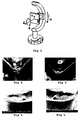
- Fig. 1 shows a goniometer set-up for the evaluation of residual stress by X-ray measurements in which
- Fig. 2 shows the wear pattern of an insert according to prior art and Fig. 3 that of an insert according to the present invention when subjected to a certain performance test.
- Fig 4. shows the result of a flaking test of an insert according to prior art and Fig 5. that of an insert according to the present invention.
- the present invention thus relates to coated cutting tool inserts comprising a body of generally polygonal or round shape having at least one rake face and at least one clearance face comprising a coating and a carbide substrate.
- the body has a composition of 6.4-8.6, preferably 7.0-8.0, most preferably 7.0-7.8, wt-% Co, 4-8.5 wt-% cubic carbides, balance WC, a CW-ratio in the range 0.78-0.92 and a surface zone of a thickness of 10-35 ⁇ m, preferably 15-25 ⁇ m, depleted from the cubic carbides TiC, TaC and/or NbC.
- the coating comprises at least one TiC x N y -layer and one well-crystalline layer of 100 % ⁇ -Al 2 O 3 .
- One such ⁇ -Al 2 O 3 layer is the top visible layer on the rake face and along the cutting edge line and it can been intensively wet blasted with a sufficiently high energy to create tensile stress relaxation in both the Al 2 O 3 and the TiC x N y -layers.
- the Al 2 O 3 top layer has a very smooth surface at least in the chip contact zone on the rake face.
- the total thickness of the two layers is ⁇ 25 ⁇ m.
- Additional layers can be incorporated into the coating structure between the substrate and the layers according to the present invention composed of metal nitrides and/or carbides and/or oxides with the metal elements selected from Ti, Nb, Hf, V, Ta, Mo, Zr, Cr, W and Al to a total coating thickness of ⁇ 5 ⁇ m.
- the residual stress, ⁇ , of the inner TIC x N y layer is determined by XRD measurements using the well known sin 2 ⁇ method as described by I.C. Noyan, J.B. Cohen, Residual Stress Measurement by Diffraction and Interpretation, Springer-Verlag, New York, 1987 (pp 117-130 ).
- the measurements are performed using CuK ⁇ -radiation on the TiC x N y (422) reflection with a goniometer setup as shown in Fig. 1.
- the measurements are carried out on an as flat surface as possible.
- the tensile stress is calculated as the average of the obtained biaxial stresses.
- the diffraction intensity ratio I(012)/I(024) is close to 1.5.
- the intensity ratio I(012)/I(024) is surprisingly significantly less than the expected value 1.5 most often ⁇ 1. This may be due to some disorder in the crystal lattice caused by the tensile stresses.
- a cutting tool insert is provided with a CVD-coating comprising a penultimate TiC x N y -layer and an outer ⁇ -Al 2 O 3 -layer.
- the Al 2 O 3 can be produced according to patent EP 0603144 giving the Al 2 O 3 -layer a crystallographic texture in 012-direction with a texture coefficient TC(012)>1.3, preferably > 1.5 or produced according to patents US 5,851,687 and US 5,702,808 giving a texture in the 110-direction with texture coefficient TC(110)> 1.5.
- the coating is subjected to a wet blasting operation with a slurry consisting of F150 grits (FEPA-standard) of Al 2 O 3 in water at an air pressure of 2.2-2.6 bar for about 10-20 sec/insert.
- the spray guns are placed approximately 100 mm from the inserts with a 90 ° spray angle.
- the insert has a different colour on the clearance side than on the black rake face.
- An outermost thin 0.1-2 ⁇ m colouring layer of TiN (yellow), TiC x N y (grey or bronze),ZrC x N y (reddish or bronze), where x ⁇ 0, y ⁇ 0 and x+y 1 or TiC (grey) is preferably deposited.
- the inserts are then blasted removing the top layer exposing the black Al 2 O 3 layer.
- the coating on the rake face will have the low desired tensile stress 50-390 MPa while the clearance side will have high tensile stresses in the range 500-700 MPa dependent on the choice of coating and the coefficient of Thermal Expansion (CTE) of the used cemented carbide insert.
- the coated insert is blasted both on the rake face and the clearance side and a coloured heat resistant paint is sprayed on the clearance side or a coloured PVD layer is deposited there in order to obtain a possibility to identify a used cutting edge.
- the saturation magnetization, M s was measured to be 0.99 hAm 2 /kg giving a CW-ratio of 0.82.
- the inserts were coated with a 0.5 ⁇ m thick layer of TiN using conventional CVD-technique at 930 °C followed by a 9 ⁇ m TiC x N y layer employing the MTCVD-technique using TiCl 4 , H 2 , N 2 and CH 3 CN as process gases at a temperature of 885 °C.
- a layer of TiC x O z about 0.5 ⁇ m thick was deposited at 1000 °C using TiCl 4 , CO and H 2 , and then the Al 2 O 3 -process was stared up by flushing the reactor with a mixture of 2 % CO 2 , 3.2 % HCl and 94.8 % H 2 for 2 min before a 7 ⁇ m thick layer of ⁇ -Al 2 O 3 was deposited. On top was a thin approx. 0.5 ⁇ m TiN layer deposited.
- T ⁇ C 012 I 012 I o 012 ⁇ 1 n ⁇ I h ⁇ k ⁇ l I O h ⁇ k ⁇ l ⁇ 1
- Coated inserts from Example 1 were post treated by the earlier mentioned blasting method under various conditions.
- the rake face of the inserts were blasted.
- Four different blasting pressures 2.0, 2.2, 2.4 and 2.6 bar and different exposure times were used.
- Some inserts were also brushed with a nylon brush containing SiC grains in order to smooth the coating surface along and near the cutting edge and some inserts were blasted according to US 5,861,210 .
- the coatings of the different post-treated inserts were examined in a Scanning Microscope (SEM) at high magnification. It was evident from the examination that some of the inserts blasted at 2.6 bar showed some minor dots of flaking of the coating at the cutting edges.
- SEM Scanning Microscope
- the smoothness of the coating surface expressed as a well known roughness value Ra was measured by AFM on an equipment from Surface Imaging System AG (SIS) on all inserts except for the brushed and the nonblasted ones.
- the roughness was measured on ten randomly selected plane surface areas (10 ⁇ mx10 ⁇ m) in the chip contact zone on rake face.
- the mean value from these ten Ra values was used as the roughness value here named mean Ra (MRa) in table 1 below.
- the residual stress was determined using ⁇ -geometry on an X-ray diffractometer Bruker D8 Discover-GADDS equipped with laser-video positioning, Euler 1/4-cradle, rotating anode as X-ray source (CuK ⁇ -radiation) and an area detector (Hi-star). A collimator of size 0.5 mm was used to focus the beam.
- the sin 2 ⁇ method was used to evaluate the residual stress using the software DIFFRAC Plus Stress32 v.
- Inserts produced according to E were tested against the high performance cutting grade GC4025 (by sales volume world's largest steel cutting grade) in an end user operation producing crankshafts. The operation involved interrupted cuts and thereby testing the toughness of the inserts.
Landscapes
- Chemical & Material Sciences (AREA)
- Metallurgy (AREA)
- Chemical Kinetics & Catalysis (AREA)
- Engineering & Computer Science (AREA)
- Materials Engineering (AREA)
- Mechanical Engineering (AREA)
- Organic Chemistry (AREA)
- General Chemical & Material Sciences (AREA)
- Inorganic Chemistry (AREA)
- Cutting Tools, Boring Holders, And Turrets (AREA)
- Chemical Vapour Deposition (AREA)
- Turning (AREA)
- Mechanical Treatment Of Semiconductor (AREA)
- Polishing Bodies And Polishing Tools (AREA)
Abstract
Description
- The present invention relates to a high performance coated cutting tool insert particularly useful for turning of steel, like low alloyed steels, carbon steels and tough hardened steels at high cutting speeds. The insert is based on WC, cubic carbides and a Co-binder phase with a cobalt enriched surface zone giving the cutting insert an excellent resistance to plastic deformation and a high toughness performance. Furthermore, the coating comprises a number of wear resistance layers which have been subjected to a surface post treatment giving the tool insert a surprisingly improved cutting performance.
- The majority of today's cutting tools are based on a cemented carbide insert coated with several hard layers like TiC, TiCxNy, TiN, TiCxNyOz and Al2O3. The sequence and the thickness of the individual layers are carefully chosen to suit different cutting application areas and work-piece materials to be cut. The most frequent employed coating techniques are Chemical Vapour Deposition (CVD) and Physical Vapour Deposition (PVD). CVD-coated inserts in particular have a tremendous advantage in terms of flank and crater wear resistance over uncoated inserts.
- The CVD technique is conducted at a rather high temperature range, 950-1050 °C. Due to this high deposition temperature and to a mismatch in the coefficients of thermal expansion between the deposited coating materials and the cemented carbide tool insert, CVD can lead to coatings with cooling cracks and high tensile stresses (sometimes up to 1000 MPa). The high tensile stresses can under some cutting conditions be a disadvantage as it may aid the cooling cracks to propagate further into the cemented carbide body and cause breakage of the cutting edge.
- In the metal cutting industry there is a constant striving to increase the cutting condition envelope, i.e., the ability to withstand higher cutting speeds without sacrificing the ability to resist fracture or chipping during interrupted cutting at low speeds,
- Important improvements in the application envelope have been achieved by combining inserts with a binder phase enriched surface zone and optimised thicker coatings.
- However, with an increasing coating thickness, the positive effect on wear resistance is out balanced by an increasing negative effect in the form of an increased risk of coating delamination and reduced toughness making the cutting tool less reliable. This applies in particular to softer work piece materials such as low carbon steels and stainless steels and when the coating thickness exceeds 5-10 µm. Further, thick coatings generally have a more uneven surface, a negative feature when cutting smearing materials like low carbon steels and stainless steel. A remedy can be to apply a post smoothing operation of the coating by brushing or by wet blasting as disclosed in several patents, e.g.,
EP 0 298 729EP 1 306 150 andEP 0 736 615US 5,861,210 the purpose has, e.g., been to achieve a smooth cutting edge and to expose the Al2O3 as the top layer on the rake face leaving the TiN on the clearance side to be used as a wear detection layer. A coating with high resistance to flaking is obtained. - Every post treatment technique that exposes a surface, e.g., a coating surface to a mechanical impact as, e.g., wet or dry blasting will have some influence on the surface finish and the stress state (σ) of the coating.
- An intensive blasting impact may lower the tensile stresses in a CVD-coating, but often this will be at the expense of lost coating surface finish by the creation of ditches along the cooling cracks or can even lead to delamination of the coating.
- A very intensive treatment may even lead to a big change in the stress state, e.g., from highly tensile to highly compressive as disclosed in
EP-A-1 311 712 , in which a dry blasting technique is used. - It has now been found that a cutting tool insert with surprisingly improved cutting performance particular in steel can be obtained if one combines a certain cemented carbide composition with a certain coating structure and thickness and then post treats the coated insert by wet-blasting under controlled tough conditions.
- The cobalt binder phase is highly alloyed with W. The content of W in the binder phase can be expressed as the CW-ratio:

wherein Ms = measured saturation magnetization in hAm2/kg and wt-% Co is the cobalt content in the cemented carbide. A low CW-ratio corresponds to a high W-content in the Co binder phase. The employed post treatment will give the coating a favourable tensile stress level, the Al2O3 layer a certain important crystallographic feature and a top surface with an excellent surface finish. - The mentioned combination with the blasting technique effectively expands the limitations of what coating thickness that can be applied without performance penalty. As a result of the invention application areas of unsurpassed width is now possible. The significant improvements achieved with respect to toughness behaviour and coating adhesion was surprising.
- To significantly change the stress state of a coating by blasting, the blasting media, e.g., Al2O3 grits have to strike the coating surface with a high impulse. The impact force can be controlled by, e.g., the blasting pulp pressure (wet blasting), the distance between blasting nozzle and coating surface, grain size of the blasting media, the concentration of the blasting media and the impact angle of the blasting jet.
- It is an object of the present invention to provide CVD-coated tool inserts with improved toughness properties.
- Fig. 1 shows a goniometer set-up for the evaluation of residual stress by X-ray measurements in which
- E = Euler ¼-cradle
- S = sample
- I = incident X-ray beam
- D = diffracted X-ray beam
- θ = diffraction angle
- ω = θ
- ψ = tilt angle along the Euler ¼-cradle
- Φ = rotation angle around the sample axis
- Fig. 2 shows the wear pattern of an insert according to prior art and Fig. 3 that of an insert according to the present invention when subjected to a certain performance test.
- Fig 4. shows the result of a flaking test of an insert according to prior art and Fig 5. that of an insert according to the present invention.
- The present invention thus relates to coated cutting tool inserts comprising a body of generally polygonal or round shape having at least one rake face and at least one clearance face comprising a coating and a carbide substrate. The body has a composition of 6.4-8.6, preferably 7.0-8.0, most preferably 7.0-7.8, wt-% Co, 4-8.5 wt-% cubic carbides, balance WC, a CW-ratio in the range 0.78-0.92 and a surface zone of a thickness of 10-35 µm, preferably 15-25 µm, depleted from the cubic carbides TiC, TaC and/or NbC. The coating comprises at least one TiCxNy-layer and one well-crystalline layer of 100 % α-Al2O3. One such α-Al2O3 layer is the top visible layer on the rake face and along the cutting edge line and it can been intensively wet blasted with a sufficiently high energy to create tensile stress relaxation in both the Al2O3 and the TiCxNy-layers. The Al2O3 top layer has a very smooth surface at least in the chip contact zone on the rake face.
- It has surprisingly been discovered that a significant improved toughness performance can be achieved if a coated cutting tool insert with a generally polygonal or round shape having at least one rake face and at least one clearance face said insert being at least partly coated produced to possess the following features:
- a penultimate TiCxNy layer with a thickness of 5-15 µm, preferably 6-13 µm, most preferably 7-13 µm, where x≥0, y≥0 and x+y=1, preferably produced by MTCVD, with tensile stresses of 50-390 MPa, preferably 50-300 MPa, most preferably 50-220 MPa and
- an outer α-Al2O3-layer with a thickness of 3-12 µm, preferably 3.5-8 µm, most preferably 4-8 µm, being the top layer on the rake face and along the edge line having a mean roughness Ra ≤ 0.12 µm, preferably ≤ 0.10 µm, at least in the chip contact zone of the rake face, measured over an area of 10 µm x 10 µm by Atomic Force Microscopy (AFM) and an XRD-diffraction intensity (peak height minus background) ratio of I(012)/I(024) ≥ 1.3, preferably ≥ 1.5.
- Preferably there is a thin 0.2-2 µm bonding layer of TiCxNyOz, x≥0, z>0 and y≥0 between the TiCxNy-layer and the α-Al2O3-layer. The total thickness of the two layers is ≤25 µm.
- Additional layers can be incorporated into the coating structure between the substrate and the layers according to the present invention composed of metal nitrides and/or carbides and/or oxides with the metal elements selected from Ti, Nb, Hf, V, Ta, Mo, Zr, Cr, W and Al to a total coating thickness of <5 µm.
- It is preferred to have some tensile stresses left in the TiCxNy layer since it was found that if compressive stresses were to be induced by blasting, very high blasting impact force was required and under such conditions flaking of the coating frequently occurred along the cutting edge. It was also found that such induced compressive stresses were not as stable with respect to temperature increase, which occurs in a cutting operation as compared to if the coating has some tensile stresses still present.
- The residual stress, σ, of the inner TICxNy layer is determined by XRD measurements using the well known sin2ψ method as described by I.C. Noyan, J.B. Cohen, Residual Stress Measurement by Diffraction and Interpretation, Springer-Verlag, New York, 1987 (pp 117-130). The measurements are performed using CuKα-radiation on the TiCxNy (422) reflection with a goniometer setup as shown in Fig. 1. The measurements are carried out on an as flat surface as possible. It is recommended to use the side-inclination technique (ψ-geometry) with six to eleven ψ-angles, equidistant within a sin2ψ-range of 0 to 0.5 (ψ=45°). An equidistant distribution of Φ-angles within a Φ-sector of 90° is also preferred. To confirm a biaxial stress state the sample shall be rotated for Φ=0° and 90° while tilted in ψ. It is recommended to investigate possible presence of shear stresses and therefore both negative and positive ψ-angles shall be measured. In the case of an Euler ¼-cradle this is accomplished by measuring the sample also at Φ=180° and 270° for the different ψ-angles. The sin2ψ method is used to evaluate the residual stress preferably using some commercially available software such as DIFFRACPlus Stress32 v. 1.04 from Bruker AXS with the constants Young's modulus, E=480 GPa and Poisson's ratio, v=0.20 in case of a MTCVD Ti(C,N)-layer and locating the reflection using the Pseudo-Voigt-Fit function. In the case of the following parameters are used: E-modulus=480 GPa and Poisson's ratio v=0.20. In case of a biaxial stress state the tensile stress is calculated as the average of the obtained biaxial stresses.
- For the α-Al2O3 it is in general not possible to use the sin2ψ technique since the required high 2θ angle XRD-reflections are often too weak. However, a useful alternative measure has been found which relates the state of the α-Al2O3 to cutting performance.
- For an α-Al2O3 powder the diffraction intensity ratio I(012)/I(024) is close to 1.5. Powder Diffraction File JCPDS No 43-1484 states the intensities I0(012)=72 and I0(024)=48. For tensile stressed (with σ about > 350 MPa) CVD α-Al2O3-layers on cemented carbide the intensity ratio I(012)/I(024) is surprisingly significantly less than the expected value 1.5 most often < 1. This may be due to some disorder in the crystal lattice caused by the tensile stresses. It has been found that when such a layer is stress released by, e.g., an intense blasting operation or if it has been completely removed from the substrate and powdered, the ratio I(012)/I(024) becomes closer, equal or even higher than 1.5 dependent. The higher the applied blasting force the higher the ratio will be. Thus, this intensity ratio can be used as an important state feature of an α-Al2O3 layer.
- According to the present invention a cutting tool insert is provided with a CVD-coating comprising a penultimate TiCxNy-layer and an outer α-Al2O3-layer. The Al2O3 can be produced according to patent
EP 0603144 giving the Al2O3-layer a crystallographic texture in 012-direction with a texture coefficient TC(012)>1.3, preferably > 1.5 or produced according to patentsUS 5,851,687 andUS 5,702,808 giving a texture in the 110-direction with texture coefficient TC(110)> 1.5. In order to obtain a high surface smoothness and low tensile stress level the coating is subjected to a wet blasting operation with a slurry consisting of F150 grits (FEPA-standard) of Al2O3 in water at an air pressure of 2.2-2.6 bar for about 10-20 sec/insert. The spray guns are placed approximately 100 mm from the inserts with a 90 ° spray angle. The insert has a different colour on the clearance side than on the black rake face. An outermost thin 0.1-2 µm colouring layer of TiN (yellow), TiCxNy (grey or bronze),ZrCxNy (reddish or bronze), where x≥0, y≥0 and x+y=1 or TiC (grey) is preferably deposited. The inserts are then blasted removing the top layer exposing the black Al2O3 layer. The coating on the rake face will have the low desired tensile stress 50-390 MPa while the clearance side will have high tensile stresses in the range 500-700 MPa dependent on the choice of coating and the coefficient of Thermal Expansion (CTE) of the used cemented carbide insert. In an other embodiment of the invention the coated insert is blasted both on the rake face and the clearance side and a coloured heat resistant paint is sprayed on the clearance side or a coloured PVD layer is deposited there in order to obtain a possibility to identify a used cutting edge. - A) Cemented carbide cutting inserts with the composition 7.5 wt-% Co, 2.9 wt-% TaC, 0.5 wt-% NbC, 1.9 wt-% TiC, 0.4 wt-% TiN, balance WC, with a surface zone (22 µm) depleted from cubic carbides. The saturation magnetization, Ms, was measured to be 0.99 hAm2/kg giving a CW-ratio of 0.82. The inserts were coated with a 0.5 µm thick layer of TiN using conventional CVD-technique at 930 °C followed by a 9 µm TiCxNy layer employing the MTCVD-technique using TiCl4, H2, N2 and CH3CN as process gases at a temperature of 885 °C. In subsequent process steps during the same coating cycle a layer of TiCxOz about 0.5 µm thick was deposited at 1000 °C using TiCl4, CO and H2, and then the Al2O3-process was stared up by flushing the reactor with a mixture of 2 % CO2, 3.2 % HCl and 94.8 % H2 for 2 min before a 7 µm thick layer of α-Al2O3 was deposited. On top was a thin approx. 0.5 µm TiN layer deposited. The process conditions during the deposition steps were as below:
TiN TiCxNy TiCxOz Al2O3-start Al2O3 Step 1 and 6 2 3 4 5 TiCl4 1.5 % 1.4 % 2 % N2 38 % 38 % CO2: 2 % 4 % CO 6 % AlCl3: 3.2 % H2S - 0.3 % HCl 3.2 % 3.2 % H2: balance balance balance balance balance CH3CN - 0.6 % Pressure: 160 mbar 60 mbar 60 mbar 60 mbar 70 mbar Temp.: 930°C 885°C 1000°C 1000°C 1000°C Time: 30 min 6 h 20 min 2 min 7 h - XRD-analysis of the deposited Al2O3 layer showed that it consisted only of the α-phase with a texture coefficient TC(012)=1.4 defined as below:

where - I(hkl) = measured intensity of the (hkl) reflection
- IO(hk1) = standard intensity of Powder Diffraction File JCPDS No 43-1484.
- n = number of reflections used in the calculation (hkl) reflections used are: (012), (104), (110), (113), (024), (116).
- Coated inserts from Example 1 were post treated by the earlier mentioned blasting method under various conditions. The rake face of the inserts were blasted. Four different blasting pressures 2.0, 2.2, 2.4 and 2.6 bar and different exposure times were used. Some inserts were also brushed with a nylon brush containing SiC grains in order to smooth the coating surface along and near the cutting edge and some inserts were blasted according to
US 5,861,210 . The coatings of the different post-treated inserts were examined in a Scanning Microscope (SEM) at high magnification. It was evident from the examination that some of the inserts blasted at 2.6 bar showed some minor dots of flaking of the coating at the cutting edges. - The smoothness of the coating surface expressed as a well known roughness value Ra was measured by AFM on an equipment from Surface Imaging System AG (SIS) on all inserts except for the brushed and the nonblasted ones. The roughness was measured on ten randomly selected plane surface areas (10µmx10µm) in the chip contact zone on rake face. The mean value from these ten Ra values was used as the roughness value here named mean Ra (MRa) in table 1 below.
- X-ray Diffraction Analysis using a Bragg-Brentano diffractometer, Siemens D5000, was used to determine the I(012)/I(024)-ratio using Cu Kα-radiation.
- The obtained I(012)/I(024)-ratio on the clearance side were < 1.5 for all variants. Corresponding measurements for the rake faces se table 1.
- The residual stress was determined using ψ-geometry on an X-ray diffractometer Bruker D8 Discover-GADDS equipped with laser-video positioning, Euler 1/4-cradle, rotating anode as X-ray source (CuKα-radiation) and an area detector (Hi-star). A collimator of size 0.5 mm was used to focus the beam. The analysis was performed on the TiCxNy (422) reflection using the goniometer settings 2θ=126°, ω=63° and Φ=0°, 90°, 180°, 270°, Eight ψ tilts between 0° and 70° were performed for each Φ-angle. The sin2ψ method was used to evaluate the residual stress using the software DIFFRACPlus Stress32 v. 1.04 from Bruker AXS with the constants Young's modulus, E=480 GPa and Poisson's ratio, v=0.20 and locating the reflection using the Pseudo-Voigt-Fit function. A biaxial stress state was confirmed and the average value was used as the residual stress value. Measurements were carried out both on the rake face and the clearance side. The obtained tensile stresses on the clearance side were within 500-700 MPa for all variants, corresponding measurements for the rake faces se table 1.
- Inserts with the different post-treatments were tested in a cutting operation with high toughness demands properties. The following conditions were used:
- Dry condition
- Cutting speed V = 120 m/min
- Feed rate f(t,min) f = 0.15*(1+t/1.5) mm/rev
- Depth of cut a = 1.5 mm
- Number of repetitions = 10
- The results from the cutting tests clearly show that the best toughness performance is achieved with the variants E, F, G and H which have the lowest tensile stresses in the TiCxNy layer. Variant C and D also have stress values significantly below those of the prior art. The highest I(012)/I(024) ratio of the Al2O3-layer and low mean Ra-values. These facts show that there exists a certain parameter space of properties which is directly related to the lifetime of cutting tool insert. Consequently a number of conditions and features have to be present simultaneously in order to achieve the high performance of the cutting tool insert.
- Inserts produced according to E were tested against the high performance cutting grade GC4025 (by sales volume world's largest steel cutting grade) in an end user operation producing crankshafts. The operation involved interrupted cuts and thereby testing the toughness of the inserts.
- The GC4025 insert suffered after 31 components a pronounced fractured edge Fig.1 while the insert produced according to E managed 41 components with only minor edge chipping Fig 2.
- In another machining test comparing E and GC4025 in case hardened steel at an end user the difference in flaking resistance is illustrated in Fig 3 and 4. Also in this case the insert produced according to the invention proved itself superior to prior art produced inserts.
| Variant | Pressure,bar/ Blasting time, s | Mean Ra- Value MRa | Median time to fracture (Minutes) | I(012)/ I(024) Al2O3 Layer | Stress in TiCxNy Layer |
| A | Brushed | ---- | 0.84 | 0.8 | 565 |
| B | 2.0 / 5 | 0.13 | 1.27 | 1.1 | 440 |
| C | 2.0 /10 | 0.11 | 1.49 | 1.3 | 383 |
| D | 2.0 /20 | 0.11 | 1.67 | 1.4 | 330 |
| E | 2.2 /10 | 0.10 | 1.92 | 1.6 | 274 |
| F | 2.4 /10 | 0.09 | 2.05 | 1.9 | 213 |
| G | 2.4 /20 | 0.08 | 2.73 | 2.2 | 185 |
| H | 2.6 /10 | 0.09 | 2.61 | 2.3 | 55 |
| B = Blasted according to C-H = Blasted according to example 2. |
Claims (5)
- A coated cutting tool insert of cemented comprising a body of generally polygonal or round shape having at least one rake face and at least one clearance face characterised in said insert having a composition of 6.4-8.6, preferably 7.0-8.0, most preferably 7.0-7.8, wt-% Co, 4-8.5 wt-% cubic carbides, balance WC, a CW-ratio in the range 0.78-0.92 and having a surface zone of a thickness of 10-35 µm, preferably 15-25 µm, depleted from the cubic carbides TiC, TaC and/or NbC, said insert being at least partly coated with a 10-25 µm thick coating including at least one layer of TiCxNy, where x≥0, y≥0 and x+y=1, preferably TiCxNy deposited by MTCVD, and an α-Al2O3-layer being the outer layer at least on the rake face and that on said at least one rake face- the TiCxNy-layer has a thickness of 5-15 µm, preferably 6.5-13 µm, most preferably 7-13 µm and a tensile stress level of 50-390 MPa, preferably 50-300 MPa and- the α-Al2O3-layer with a thickness of 3-12 µm, preferably 3.5-8, most preferably 4-8 µm is the outermost layer with an XRD-diffraction intensity ratio I(012)/I(024) >1.3, preferably ≥1.5 and with a mean Ra value MRa ≤ 0.12 µm, preferably ≤ 0.10 µm, at least in the chip contact zone on the rake face, as measured on ten randomly selected areas 10×10 µm2 by AFM-technique and on said clearance face- the TiCxNy-layer has a tensile stress in the range 500-700 MPa and that and- the α-Al2O3-layer has an XRD-diffraction intensity ratio I(012)/I(024)<1.5, preferably covered with a thin 0.1-2 µm TiN, TiCxNy, ZrCxNy or TiC layer giving the insert a different colour on that face
or on said at least one rake phase and said at least one clearance side- the TiCxNy-layer has a thickness of 5-15 µm, preferably 6-13 µm, most preferably 7-13 µm and a tensile stress level of 50-390 MPa, preferably 50-300 MPa and- the α-Al2O3-layer with a thickness of 3-12 µm, preferably 3.5-8 µm, preferably 4-8 µm has an XRD-diffraction intensity ratio I(012)/I(024) ≥1.3, preferably ≥1.5 and on the rake phase is the outermost layer with a mean Ra value MRa ≤ 0.12 µm, preferably ≤ 0.10 µm, at least in the chip contact zone on the rake face, as measured on ten randomly selected areas 10×10 µm2 by AFM-technique and on that said clearance face the top layer consists of a coloured heat resistant paint or a coloured PVD-layer. - A cutting tool insert according to the preceding claim
characterized in having a thin 0.2-2 µm TiCxNyOz bonding layer, x≥0, z>0 and y≥0, between the TiCxNy- and the Al2O3-layer. - A cutting tool insert according to any of the preceding claims characterized the α-Al2O3-layer having a texture in the 012-direction with a texture coefficient TC(012)>1.3, preferably TC(012)> 1.5.
- A cutting tool insert according to any of the preceding claims characterized the α-Al2O3-layer having a texture in the 110-direction with a texture coefficient TC(110)>1.5.
- A cutting tool insert according to any of the preceding claims characterized the coating containing additional layers composed of metal nitrides and/or carbides and/or oxides with the metal elements selected from Ti, Nb, Hf, V, Ta, Mo, Zr, Cr, W and Al to a total layer thickness of <5 µm.
Applications Claiming Priority (1)
| Application Number | Priority Date | Filing Date | Title |
|---|---|---|---|
| SE0501410A SE529023C2 (en) | 2005-06-17 | 2005-06-17 | Coated carbide cutter |
Publications (2)
| Publication Number | Publication Date |
|---|---|
| EP1734155A1 true EP1734155A1 (en) | 2006-12-20 |
| EP1734155B1 EP1734155B1 (en) | 2008-08-13 |
Family
ID=36822369
Family Applications (2)
| Application Number | Title | Priority Date | Filing Date |
|---|---|---|---|
| EP06445040A Active EP1734155B1 (en) | 2005-06-17 | 2006-06-07 | Coated cutting tool insert |
| EP06747919A Active EP1893786B1 (en) | 2005-06-17 | 2006-06-16 | A method of producing metal cutting tools |
Family Applications After (1)
| Application Number | Title | Priority Date | Filing Date |
|---|---|---|---|
| EP06747919A Active EP1893786B1 (en) | 2005-06-17 | 2006-06-16 | A method of producing metal cutting tools |
Country Status (10)
| Country | Link |
|---|---|
| US (2) | US8318293B2 (en) |
| EP (2) | EP1734155B1 (en) |
| JP (3) | JP2007007847A (en) |
| KR (2) | KR20080018890A (en) |
| CN (2) | CN101198720A (en) |
| AT (2) | ATE404712T1 (en) |
| DE (1) | DE602006002179D1 (en) |
| IL (2) | IL176253A0 (en) |
| SE (1) | SE529023C2 (en) |
| WO (2) | WO2006135330A1 (en) |
Cited By (9)
| Publication number | Priority date | Publication date | Assignee | Title |
|---|---|---|---|---|
| EP1696051A1 (en) | 2005-02-25 | 2006-08-30 | Sandvik Intellectual Property AB | Coated cutting tool insert |
| EP1867756A2 (en) * | 2006-06-16 | 2007-12-19 | Sandvik Intellectual Property AB | Coated cutting tool insert |
| EP1893786A1 (en) * | 2005-06-17 | 2008-03-05 | Sandvik Intellectual Property AB | A method of producing metal cutting tools |
| WO2008094105A1 (en) * | 2007-02-01 | 2008-08-07 | Seco Tools Ab | Coated cutting tool for medium- rough to rough turning of stainless steels and superalloys |
| WO2008094104A1 (en) * | 2007-02-01 | 2008-08-07 | Seco Tools Ab | Coated cutting tool for fine to medium-rough turning of stainless steels |
| US7754316B2 (en) | 2006-10-18 | 2010-07-13 | Sandvik Intellectual Property Ab | Coated cutting tool insert |
| US7799413B2 (en) | 2005-06-17 | 2010-09-21 | Sandvik Intellectual Property Ab | Coated cutting tool insert |
| EP2499273A4 (en) * | 2009-11-10 | 2015-11-18 | Kennametal Inc | Coated cutting insert and method for making the same |
| CN108411178A (en) * | 2018-04-12 | 2018-08-17 | 明光市天淼新能源科技有限公司 | A kind of cemented carbide material |
Families Citing this family (25)
| Publication number | Priority date | Publication date | Assignee | Title |
|---|---|---|---|---|
| DE602007008639D1 (en) * | 2006-06-16 | 2010-10-07 | Sandvik Intellectual Property | Coated cutting tool insert |
| SE530756C2 (en) | 2006-09-15 | 2008-09-02 | Sandvik Intellectual Property | Methods of Manufacturing a Coated Cement Cutting Tool, a Coated Cutting Tool and a Coated Rotating Cutting Tool |
| US8080323B2 (en) | 2007-06-28 | 2011-12-20 | Kennametal Inc. | Cutting insert with a wear-resistant coating scheme exhibiting wear indication and method of making the same |
| US8475944B2 (en) * | 2007-06-28 | 2013-07-02 | Kennametal Inc. | Coated ceramic cutting insert and method for making the same |
| US8557406B2 (en) | 2007-06-28 | 2013-10-15 | Kennametal Inc. | Coated PCBN cutting insert, coated PCBN cutting tool using such coated PCBN cutting insert, and method for making the same |
| US20090004449A1 (en) * | 2007-06-28 | 2009-01-01 | Zhigang Ban | Cutting insert with a wear-resistant coating scheme exhibiting wear indication and method of making the same |
| WO2009070107A1 (en) * | 2007-11-28 | 2009-06-04 | Sandvik Intellectual Property Ab | Coated cutting tool insert |
| CN101842179B (en) * | 2008-04-30 | 2012-11-28 | 住友电气工业株式会社 | Surface coated cutting tool |
| SE533154C2 (en) * | 2008-12-18 | 2010-07-06 | Seco Tools Ab | Improved coated cutting for rough turning |
| EP2287359B1 (en) * | 2009-07-03 | 2012-05-23 | Sandvik Intellectual Property AB | Coated cutting tool insert |
| JP5672444B2 (en) * | 2010-11-12 | 2015-02-18 | 三菱マテリアル株式会社 | Surface coated drill with excellent wear resistance and chip evacuation |
| US8507082B2 (en) | 2011-03-25 | 2013-08-13 | Kennametal Inc. | CVD coated polycrystalline c-BN cutting tools |
| CN103160723B (en) * | 2011-12-15 | 2015-10-28 | 株洲钻石切削刀具股份有限公司 | A kind of Wimet for the general process tool of steel and coated chip thereof |
| CN103160724B (en) * | 2011-12-15 | 2015-11-04 | 株洲钻石切削刀具股份有限公司 | A kind of Wimet for cast iron turnery processing and hard alloy coated blade thereof |
| US9028953B2 (en) | 2013-01-11 | 2015-05-12 | Kennametal Inc. | CVD coated polycrystalline c-BN cutting tools |
| FR3035607B1 (en) * | 2015-04-30 | 2017-04-28 | Saint-Gobain Centre De Rech Et D'Etudes Europeen | METHOD FOR MODIFYING THE APPEARANCE OF A SURFACE |
| JP6699056B2 (en) | 2016-06-14 | 2020-05-27 | 住友電工ハードメタル株式会社 | Surface coated cutting tool |
| EP3263743A1 (en) * | 2016-06-29 | 2018-01-03 | Sandvik Intellectual Property AB | Cvd coated cutting tool |
| KR101687142B1 (en) | 2016-07-20 | 2016-12-15 | 한국야금 주식회사 | Hard coated layer for cutting tools |
| JP6690102B2 (en) | 2016-08-25 | 2020-04-28 | 住友電工ハードメタル株式会社 | Surface-coated cutting tool and manufacturing method thereof |
| JP6728551B2 (en) | 2016-08-25 | 2020-07-22 | 住友電工ハードメタル株式会社 | Surface-coated cutting tool and manufacturing method thereof |
| CN106929823A (en) * | 2017-03-12 | 2017-07-07 | 苏州南尔材料科技有限公司 | A kind of method that use sedimentation prepares thin film of titanium oxide on a silicon substrate |
| CN107775538A (en) * | 2017-09-15 | 2018-03-09 | 富耐克超硬材料股份有限公司 | Diamond-coated tools and its post-processing approach |
| CN107620053A (en) * | 2017-11-01 | 2018-01-23 | 南通欧科数控设备有限公司 | A kind of manufacture method for cutting coated cutting tool |
| JP6784345B1 (en) * | 2019-02-19 | 2020-11-11 | 住友電工ハードメタル株式会社 | Cutting tools |
Citations (11)
| Publication number | Priority date | Publication date | Assignee | Title |
|---|---|---|---|---|
| EP0298729A1 (en) * | 1987-07-10 | 1989-01-11 | Sumitomo Electric Industries Limited | Cutting tool |
| EP0603144A1 (en) | 1992-12-18 | 1994-06-22 | Sandvik Aktiebolag | Oxide coated cutting tool |
| EP0659903A1 (en) | 1993-12-23 | 1995-06-28 | Sandvik Aktiebolag | Alumina coated cutting tool |
| EP0693574A1 (en) * | 1994-07-20 | 1996-01-24 | Sandvik Aktiebolag | Aluminium oxide coated tool |
| EP0736615A2 (en) | 1995-04-05 | 1996-10-09 | Sandvik Aktiebolag | Coated cutting insert |
| US5702808A (en) * | 1994-11-15 | 1997-12-30 | Sandvik Ab | Al2 O2 -coated cutting tool preferably for near net shape machining |
| US5863640A (en) | 1995-07-14 | 1999-01-26 | Sandvik Ab | Coated cutting insert and method of manufacture thereof |
| WO1999023275A1 (en) * | 1997-11-03 | 1999-05-14 | Seco Tools Ab | Cemented carbide body with high wear resistance and extra tough behaviour |
| US5945207A (en) | 1996-09-06 | 1999-08-31 | Sandvik Ab | Coated cutting insert |
| US20030104254A1 (en) * | 2001-03-27 | 2003-06-05 | Hartmut Westphal | Method for increasing compression stress or reducing internal tension stress of a cvd, pcvd or pvd layer and cutting insert for machining |
| EP1464727A2 (en) | 2003-04-01 | 2004-10-06 | Sandvik AB | Oxide coated cutting tool |
Family Cites Families (45)
| Publication number | Priority date | Publication date | Assignee | Title |
|---|---|---|---|---|
| US2350440A (en) * | 1942-04-29 | 1944-06-06 | Gen Motors Corp | Shot blasting test |
| US4125969A (en) * | 1977-01-25 | 1978-11-21 | A. Long & Company Limited | Wet abrasion blasting |
| US4497874A (en) * | 1983-04-28 | 1985-02-05 | General Electric Company | Coated carbide cutting tool insert |
| JPS59219122A (en) * | 1983-05-27 | 1984-12-10 | Sumitomo Electric Ind Ltd | Covered sintered hard alloy tool and manufacturing method thereof |
| US4674365A (en) * | 1983-07-27 | 1987-06-23 | Spectra Products Corporation | Method for extending the life of a cutting tool |
| JPS60184627A (en) | 1984-03-02 | 1985-09-20 | Toyota Motor Corp | Method for subjecting metallic member to shot peening |
| JPH02180559A (en) * | 1988-12-28 | 1990-07-13 | Nissan Motor Co Ltd | Shot peening device |
| JP2757581B2 (en) | 1991-03-28 | 1998-05-25 | 三菱マテリアル株式会社 | Surface coated cutting tool |
| JP3021742B2 (en) | 1991-03-28 | 2000-03-15 | 三菱マテリアル株式会社 | Surface coated cemented carbide cutting tool |
| US5258098A (en) * | 1991-06-17 | 1993-11-02 | Cycam, Inc. | Method of production of a surface adapted to promote adhesion |
| JPH05163423A (en) | 1991-12-17 | 1993-06-29 | Kanebo Ltd | Polyethylene terephthalate resin composition for blasting material |
| JP3236899B2 (en) * | 1992-08-11 | 2001-12-10 | 三菱マテリアル株式会社 | Manufacturing method of surface coated tungsten carbide based cemented carbide cutting tool with excellent wear and fracture resistance |
| JP2603177B2 (en) | 1992-09-29 | 1997-04-23 | 東芝タンガロイ株式会社 | Coated sintered alloy with excellent fracture resistance |
| JPH06116641A (en) | 1992-10-05 | 1994-04-26 | Sumitomo Metal Ind Ltd | Production of silicon steel sheet for compact stationary device |
| JPH06246637A (en) | 1993-02-19 | 1994-09-06 | Kanmeta Eng Kk | Method for preventing metal thermal fatigue and progress of stress corrosion cracking by zirconia shot blast |
| JP3424263B2 (en) | 1993-05-27 | 2003-07-07 | 住友電気工業株式会社 | Coated hard alloy members |
| JPH07173643A (en) * | 1993-12-21 | 1995-07-11 | Mazda Motor Corp | Method for phosphating metal surface and phosphating solution |
| SE502223C2 (en) * | 1994-01-14 | 1995-09-18 | Sandvik Ab | Methods and articles when coating a cutting tool with an alumina layer |
| US5786069A (en) * | 1995-09-01 | 1998-07-28 | Sandvik Ab | Coated turning insert |
| DE69619275T2 (en) * | 1995-11-30 | 2004-06-24 | Sandvik Ab | COATED ROTATABLE INSERT AND METHOD FOR THE PRODUCTION THEREOF |
| US6120570A (en) * | 1996-02-14 | 2000-09-19 | Smith International | Process for manufacturing inserts with holes for clamping |
| JP3560303B2 (en) | 1996-11-29 | 2004-09-02 | 日立金属株式会社 | Aluminum oxide coated tool and method of manufacturing the same |
| SE511211C2 (en) | 1996-12-20 | 1999-08-23 | Sandvik Ab | A multilayer coated polycrystalline cubic boron nitride cutting tool |
| JP3658949B2 (en) * | 1997-11-04 | 2005-06-15 | 住友電気工業株式会社 | Coated cemented carbide |
| SE516017C2 (en) * | 1999-02-05 | 2001-11-12 | Sandvik Ab | Cemented carbide inserts coated with durable coating |
| SE9901244D0 (en) * | 1999-04-08 | 1999-04-08 | Sandvik Ab | Cemented carbide insert |
| DE19924422C2 (en) | 1999-05-28 | 2001-03-08 | Cemecon Ceramic Metal Coatings | Process for producing a hard-coated component and coated, after-treated component |
| JP4029529B2 (en) * | 1999-07-23 | 2008-01-09 | 三菱マテリアル株式会社 | Surface coated tungsten carbide based cemented carbide cutting tool with excellent chipping resistance with hard coating layer in intermittent heavy cutting |
| KR100688923B1 (en) * | 2000-07-12 | 2007-03-09 | 스미토모덴키고교가부시키가이샤 | Coated cutting tool |
| US6554548B1 (en) * | 2000-08-11 | 2003-04-29 | Kennametal Inc. | Chromium-containing cemented carbide body having a surface zone of binder enrichment |
| SE522736C2 (en) | 2001-02-16 | 2004-03-02 | Sandvik Ab | Aluminum-coated cutting tool and method for making the same |
| JP2002370105A (en) | 2001-06-19 | 2002-12-24 | Toshiba Tungaloy Co Ltd | Aluminum oxide coated-tool |
| JP2003025114A (en) * | 2001-07-16 | 2003-01-29 | Toshiba Tungaloy Co Ltd | Aluminium oxide coated cutting tool |
| JP5054871B2 (en) | 2001-09-03 | 2012-10-24 | キヤノン株式会社 | Method for producing developer carrier |
| JP3622846B2 (en) * | 2001-09-21 | 2005-02-23 | 住友電気工業株式会社 | Sticky milling tool |
| SE525581C2 (en) * | 2002-05-08 | 2005-03-15 | Seco Tools Ab | Cutting coated with alumina made with CVD |
| KR20060101481A (en) * | 2003-10-28 | 2006-09-25 | 베헤르 게엠베하 운트 콤파니 카게 | Flow channel for a heat exchanger, and heat exchanger having flow passage of this type |
| JP4300104B2 (en) | 2003-12-16 | 2009-07-22 | 大日本住友製薬株式会社 | Method for analyzing (1-hydroxyethylidene) bisphosphonate |
| JP2006026814A (en) * | 2004-07-16 | 2006-02-02 | Tungaloy Corp | Coated cutting tip |
| SE528107C2 (en) * | 2004-10-04 | 2006-09-05 | Sandvik Intellectual Property | Coated carbide inserts, especially useful for high-speed machining of metallic workpieces |
| WO2006064724A1 (en) | 2004-12-14 | 2006-06-22 | Sumitomo Electric Hardmetal Corp. | Surface-covered cutting tool |
| SE528696C2 (en) * | 2005-02-25 | 2007-01-23 | Sandvik Intellectual Property | CVD-coated carbide, cermet or ceramic cutter and ways of manufacturing the same |
| US20070298282A1 (en) * | 2005-06-17 | 2007-12-27 | Sandvik Intellectual Property Ab | Coated cutting tool insert |
| SE529023C2 (en) | 2005-06-17 | 2007-04-10 | Sandvik Intellectual Property | Coated carbide cutter |
| SE530735C2 (en) * | 2006-10-18 | 2008-08-26 | Sandvik Intellectual Property | A coated carbide cutter, especially useful for turning steel |
-
2005
- 2005-06-17 SE SE0501410A patent/SE529023C2/en not_active IP Right Cessation
-
2006
- 2006-06-07 EP EP06445040A patent/EP1734155B1/en active Active
- 2006-06-07 DE DE602006002179T patent/DE602006002179D1/en active Active
- 2006-06-07 AT AT06445040T patent/ATE404712T1/en active
- 2006-06-12 IL IL176253A patent/IL176253A0/en unknown
- 2006-06-16 WO PCT/SE2006/000736 patent/WO2006135330A1/en active Application Filing
- 2006-06-16 US US11/454,127 patent/US8318293B2/en active Active
- 2006-06-16 WO PCT/SE2006/000727 patent/WO2006135325A1/en active Application Filing
- 2006-06-16 EP EP06747919A patent/EP1893786B1/en active Active
- 2006-06-16 JP JP2006167831A patent/JP2007007847A/en not_active Withdrawn
- 2006-06-16 CN CNA200680021583XA patent/CN101198720A/en active Pending
- 2006-06-16 KR KR1020077029171A patent/KR20080018890A/en not_active Application Discontinuation
- 2006-06-16 US US11/922,132 patent/US8409668B2/en active Active
- 2006-06-16 AT AT06747919T patent/ATE519871T1/en active
- 2006-06-16 JP JP2008516789A patent/JP5087736B2/en active Active
- 2006-06-17 KR KR1020060054646A patent/KR101334577B1/en active IP Right Grant
- 2006-06-19 CN CNB2006100938008A patent/CN100469498C/en not_active Expired - Fee Related
-
2007
- 2007-11-27 IL IL187684A patent/IL187684A0/en unknown
-
2012
- 2012-07-30 JP JP2012168009A patent/JP5670972B2/en active Active
Patent Citations (13)
| Publication number | Priority date | Publication date | Assignee | Title |
|---|---|---|---|---|
| EP0298729A1 (en) * | 1987-07-10 | 1989-01-11 | Sumitomo Electric Industries Limited | Cutting tool |
| EP0603144A1 (en) | 1992-12-18 | 1994-06-22 | Sandvik Aktiebolag | Oxide coated cutting tool |
| US5851687A (en) | 1993-12-23 | 1998-12-22 | Sandvik Ab | Alumina coated cutting tool |
| EP0659903A1 (en) | 1993-12-23 | 1995-06-28 | Sandvik Aktiebolag | Alumina coated cutting tool |
| EP0693574A1 (en) * | 1994-07-20 | 1996-01-24 | Sandvik Aktiebolag | Aluminium oxide coated tool |
| US5861210A (en) | 1994-07-20 | 1999-01-19 | Sandvik Ab | Aluminum oxide coated tool |
| US5702808A (en) * | 1994-11-15 | 1997-12-30 | Sandvik Ab | Al2 O2 -coated cutting tool preferably for near net shape machining |
| EP0736615A2 (en) | 1995-04-05 | 1996-10-09 | Sandvik Aktiebolag | Coated cutting insert |
| US5863640A (en) | 1995-07-14 | 1999-01-26 | Sandvik Ab | Coated cutting insert and method of manufacture thereof |
| US5945207A (en) | 1996-09-06 | 1999-08-31 | Sandvik Ab | Coated cutting insert |
| WO1999023275A1 (en) * | 1997-11-03 | 1999-05-14 | Seco Tools Ab | Cemented carbide body with high wear resistance and extra tough behaviour |
| US20030104254A1 (en) * | 2001-03-27 | 2003-06-05 | Hartmut Westphal | Method for increasing compression stress or reducing internal tension stress of a cvd, pcvd or pvd layer and cutting insert for machining |
| EP1464727A2 (en) | 2003-04-01 | 2004-10-06 | Sandvik AB | Oxide coated cutting tool |
Non-Patent Citations (5)
| Title |
|---|
| J. GLUHMANN, DIPLOMARBEIT, 2004, pages 54 - 57, XP003028186 |
| K. WEINERT: "Spanende Fertigung, 4e Ausgabe", 2005, pages: 181 - 188, XP003028187 |
| MARITZEN W. ET AL: "Lattice Parameters and Saturation Magnetization of Co-W-C Alloys", POWDER METALLURGY INTERNATIONAL, vol. 17, no. 2, 1985, pages 68 - 71, XP000569241 |
| ROEBUCK B. ET AL: "Magnetic moment (Saturation) measurements on hardmetals", INT.J. OF REFRACTORY METALS & HARD MATERIALS, vol. 14, 1996, pages 419 - 424, XP003028188 |
| SCHEDLER W.: "Hartmetall fur den Praktiker", 1988, VDI-VERLAG GMBH, pages: 43 - 57, XP003028189 |
Cited By (14)
| Publication number | Priority date | Publication date | Assignee | Title |
|---|---|---|---|---|
| EP1696051A1 (en) | 2005-02-25 | 2006-08-30 | Sandvik Intellectual Property AB | Coated cutting tool insert |
| EP1893786A1 (en) * | 2005-06-17 | 2008-03-05 | Sandvik Intellectual Property AB | A method of producing metal cutting tools |
| US8409668B2 (en) | 2005-06-17 | 2013-04-02 | Sandvik Intellectual Property Ab | Method of producing metal cutting tools |
| US7799413B2 (en) | 2005-06-17 | 2010-09-21 | Sandvik Intellectual Property Ab | Coated cutting tool insert |
| EP1893786A4 (en) * | 2005-06-17 | 2009-12-02 | Sandvik Intellectual Property | A method of producing metal cutting tools |
| EP1867756A2 (en) * | 2006-06-16 | 2007-12-19 | Sandvik Intellectual Property AB | Coated cutting tool insert |
| EP1867755A2 (en) | 2006-06-16 | 2007-12-19 | Sandvik Intellectual Property AB | Coated cutting tool insert |
| EP1867756A3 (en) * | 2006-06-16 | 2008-07-02 | Sandvik Intellectual Property AB | Coated cutting tool insert |
| EP1867755A3 (en) * | 2006-06-16 | 2008-07-02 | Sandvik Intellectual Property AB | Coated cutting tool insert |
| US7754316B2 (en) | 2006-10-18 | 2010-07-13 | Sandvik Intellectual Property Ab | Coated cutting tool insert |
| WO2008094104A1 (en) * | 2007-02-01 | 2008-08-07 | Seco Tools Ab | Coated cutting tool for fine to medium-rough turning of stainless steels |
| WO2008094105A1 (en) * | 2007-02-01 | 2008-08-07 | Seco Tools Ab | Coated cutting tool for medium- rough to rough turning of stainless steels and superalloys |
| EP2499273A4 (en) * | 2009-11-10 | 2015-11-18 | Kennametal Inc | Coated cutting insert and method for making the same |
| CN108411178A (en) * | 2018-04-12 | 2018-08-17 | 明光市天淼新能源科技有限公司 | A kind of cemented carbide material |
Also Published As
| Publication number | Publication date |
|---|---|
| EP1893786A4 (en) | 2009-12-02 |
| EP1734155B1 (en) | 2008-08-13 |
| CN1879991A (en) | 2006-12-20 |
| US8318293B2 (en) | 2012-11-27 |
| SE0501410L (en) | 2006-12-18 |
| US20090068371A1 (en) | 2009-03-12 |
| US8409668B2 (en) | 2013-04-02 |
| IL187684A0 (en) | 2008-08-07 |
| WO2006135325A1 (en) | 2006-12-21 |
| JP5087736B2 (en) | 2012-12-05 |
| KR101334577B1 (en) | 2013-11-28 |
| JP5670972B2 (en) | 2015-02-18 |
| SE529023C2 (en) | 2007-04-10 |
| EP1893786A1 (en) | 2008-03-05 |
| CN100469498C (en) | 2009-03-18 |
| ATE519871T1 (en) | 2011-08-15 |
| JP2007007847A (en) | 2007-01-18 |
| KR20080018890A (en) | 2008-02-28 |
| CN101198720A (en) | 2008-06-11 |
| WO2006135330A1 (en) | 2006-12-21 |
| KR20060132507A (en) | 2006-12-21 |
| DE602006002179D1 (en) | 2008-09-25 |
| US20070009763A1 (en) | 2007-01-11 |
| IL176253A0 (en) | 2006-10-05 |
| EP1893786B1 (en) | 2011-08-10 |
| ATE404712T1 (en) | 2008-08-15 |
| JP2008546546A (en) | 2008-12-25 |
| JP2012213853A (en) | 2012-11-08 |
Similar Documents
| Publication | Publication Date | Title |
|---|---|---|
| EP1734155B1 (en) | Coated cutting tool insert | |
| EP1696051B1 (en) | Coated cutting tool insert and fabrication method | |
| US7754316B2 (en) | Coated cutting tool insert | |
| EP1867755B1 (en) | Coated cutting tool insert | |
| US7799413B2 (en) | Coated cutting tool insert | |
| EP2287359B1 (en) | Coated cutting tool insert | |
| EP1772217B1 (en) | Surface coated cutting tool | |
| EP0753603A2 (en) | Coated cutting insert | |
| EP2074241B1 (en) | Coated cutting tool | |
| KR101444457B1 (en) | Coated cutting tool insert | |
| WO2009070107A1 (en) | Coated cutting tool insert |
Legal Events
| Date | Code | Title | Description |
|---|---|---|---|
| PUAI | Public reference made under article 153(3) epc to a published international application that has entered the european phase |
Free format text: ORIGINAL CODE: 0009012 |
|
| AK | Designated contracting states |
Kind code of ref document: A1 Designated state(s): AT BE BG CH CY CZ DE DK EE ES FI FR GB GR HU IE IS IT LI LT LU LV MC NL PL PT RO SE SI SK TR |
|
| AX | Request for extension of the european patent |
Extension state: AL BA HR MK YU |
|
| 17P | Request for examination filed |
Effective date: 20070620 |
|
| 17Q | First examination report despatched |
Effective date: 20070719 |
|
| AKX | Designation fees paid |
Designated state(s): AT BE BG CH CY CZ DE DK EE ES FI FR GB GR HU IE IS IT LI LT LU LV MC NL PL PT RO SE SI SK TR |
|
| GRAP | Despatch of communication of intention to grant a patent |
Free format text: ORIGINAL CODE: EPIDOSNIGR1 |
|
| GRAS | Grant fee paid |
Free format text: ORIGINAL CODE: EPIDOSNIGR3 |
|
| GRAA | (expected) grant |
Free format text: ORIGINAL CODE: 0009210 |
|
| AK | Designated contracting states |
Kind code of ref document: B1 Designated state(s): AT BE BG CH CY CZ DE DK EE ES FI FR GB GR HU IE IS IT LI LT LU LV MC NL PL PT RO SE SI SK TR |
|
| REG | Reference to a national code |
Ref country code: GB Ref legal event code: FG4D |
|
| REG | Reference to a national code |
Ref country code: CH Ref legal event code: NV Representative=s name: BOVARD AG PATENTANWAELTE Ref country code: CH Ref legal event code: EP |
|
| REG | Reference to a national code |
Ref country code: IE Ref legal event code: FG4D |
|
| REF | Corresponds to: |
Ref document number: 602006002179 Country of ref document: DE Date of ref document: 20080925 Kind code of ref document: P |
|
| REG | Reference to a national code |
Ref country code: SE Ref legal event code: TRGR |
|
| PG25 | Lapsed in a contracting state [announced via postgrant information from national office to epo] |
Ref country code: LT Free format text: LAPSE BECAUSE OF FAILURE TO SUBMIT A TRANSLATION OF THE DESCRIPTION OR TO PAY THE FEE WITHIN THE PRESCRIBED TIME-LIMIT Effective date: 20080813 Ref country code: IS Free format text: LAPSE BECAUSE OF FAILURE TO SUBMIT A TRANSLATION OF THE DESCRIPTION OR TO PAY THE FEE WITHIN THE PRESCRIBED TIME-LIMIT Effective date: 20081213 Ref country code: NL Free format text: LAPSE BECAUSE OF FAILURE TO SUBMIT A TRANSLATION OF THE DESCRIPTION OR TO PAY THE FEE WITHIN THE PRESCRIBED TIME-LIMIT Effective date: 20080813 |
|
| PG25 | Lapsed in a contracting state [announced via postgrant information from national office to epo] |
Ref country code: LV Free format text: LAPSE BECAUSE OF FAILURE TO SUBMIT A TRANSLATION OF THE DESCRIPTION OR TO PAY THE FEE WITHIN THE PRESCRIBED TIME-LIMIT Effective date: 20080813 Ref country code: SI Free format text: LAPSE BECAUSE OF FAILURE TO SUBMIT A TRANSLATION OF THE DESCRIPTION OR TO PAY THE FEE WITHIN THE PRESCRIBED TIME-LIMIT Effective date: 20080813 Ref country code: FI Free format text: LAPSE BECAUSE OF FAILURE TO SUBMIT A TRANSLATION OF THE DESCRIPTION OR TO PAY THE FEE WITHIN THE PRESCRIBED TIME-LIMIT Effective date: 20080813 Ref country code: ES Free format text: LAPSE BECAUSE OF FAILURE TO SUBMIT A TRANSLATION OF THE DESCRIPTION OR TO PAY THE FEE WITHIN THE PRESCRIBED TIME-LIMIT Effective date: 20081124 |
|
| PG25 | Lapsed in a contracting state [announced via postgrant information from national office to epo] |
Ref country code: BE Free format text: LAPSE BECAUSE OF FAILURE TO SUBMIT A TRANSLATION OF THE DESCRIPTION OR TO PAY THE FEE WITHIN THE PRESCRIBED TIME-LIMIT Effective date: 20080813 |
|
| PG25 | Lapsed in a contracting state [announced via postgrant information from national office to epo] |
Ref country code: BG Free format text: LAPSE BECAUSE OF FAILURE TO SUBMIT A TRANSLATION OF THE DESCRIPTION OR TO PAY THE FEE WITHIN THE PRESCRIBED TIME-LIMIT Effective date: 20081113 Ref country code: DK Free format text: LAPSE BECAUSE OF FAILURE TO SUBMIT A TRANSLATION OF THE DESCRIPTION OR TO PAY THE FEE WITHIN THE PRESCRIBED TIME-LIMIT Effective date: 20080813 |
|
| PLBI | Opposition filed |
Free format text: ORIGINAL CODE: 0009260 |
|
| PG25 | Lapsed in a contracting state [announced via postgrant information from national office to epo] |
Ref country code: CZ Free format text: LAPSE BECAUSE OF FAILURE TO SUBMIT A TRANSLATION OF THE DESCRIPTION OR TO PAY THE FEE WITHIN THE PRESCRIBED TIME-LIMIT Effective date: 20080813 Ref country code: RO Free format text: LAPSE BECAUSE OF FAILURE TO SUBMIT A TRANSLATION OF THE DESCRIPTION OR TO PAY THE FEE WITHIN THE PRESCRIBED TIME-LIMIT Effective date: 20080813 Ref country code: SK Free format text: LAPSE BECAUSE OF FAILURE TO SUBMIT A TRANSLATION OF THE DESCRIPTION OR TO PAY THE FEE WITHIN THE PRESCRIBED TIME-LIMIT Effective date: 20080813 Ref country code: PT Free format text: LAPSE BECAUSE OF FAILURE TO SUBMIT A TRANSLATION OF THE DESCRIPTION OR TO PAY THE FEE WITHIN THE PRESCRIBED TIME-LIMIT Effective date: 20090113 |
|
| PLAX | Notice of opposition and request to file observation + time limit sent |
Free format text: ORIGINAL CODE: EPIDOSNOBS2 |
|
| 26 | Opposition filed |
Opponent name: KENNAMETAL TECHNOLOGIES GMBH Effective date: 20090513 |
|
| PG25 | Lapsed in a contracting state [announced via postgrant information from national office to epo] |
Ref country code: EE Free format text: LAPSE BECAUSE OF FAILURE TO SUBMIT A TRANSLATION OF THE DESCRIPTION OR TO PAY THE FEE WITHIN THE PRESCRIBED TIME-LIMIT Effective date: 20080813 |
|
| PLAF | Information modified related to communication of a notice of opposition and request to file observations + time limit |
Free format text: ORIGINAL CODE: EPIDOSCOBS2 |
|
| PLBB | Reply of patent proprietor to notice(s) of opposition received |
Free format text: ORIGINAL CODE: EPIDOSNOBS3 |
|
| PG25 | Lapsed in a contracting state [announced via postgrant information from national office to epo] |
Ref country code: MC Free format text: LAPSE BECAUSE OF NON-PAYMENT OF DUE FEES Effective date: 20090630 |
|
| PG25 | Lapsed in a contracting state [announced via postgrant information from national office to epo] |
Ref country code: IE Free format text: LAPSE BECAUSE OF NON-PAYMENT OF DUE FEES Effective date: 20090607 |
|
| PG25 | Lapsed in a contracting state [announced via postgrant information from national office to epo] |
Ref country code: PL Free format text: LAPSE BECAUSE OF FAILURE TO SUBMIT A TRANSLATION OF THE DESCRIPTION OR TO PAY THE FEE WITHIN THE PRESCRIBED TIME-LIMIT Effective date: 20080813 |
|
| PG25 | Lapsed in a contracting state [announced via postgrant information from national office to epo] |
Ref country code: GR Free format text: LAPSE BECAUSE OF FAILURE TO SUBMIT A TRANSLATION OF THE DESCRIPTION OR TO PAY THE FEE WITHIN THE PRESCRIBED TIME-LIMIT Effective date: 20081114 |
|
| REG | Reference to a national code |
Ref country code: CH Ref legal event code: PFA Owner name: SANDVIK INTELLECTUAL PROPERTY AB Free format text: SANDVIK INTELLECTUAL PROPERTY AB# #811 81 SANDVIKEN (SE) -TRANSFER TO- SANDVIK INTELLECTUAL PROPERTY AB# #811 81 SANDVIKEN (SE) |
|
| PG25 | Lapsed in a contracting state [announced via postgrant information from national office to epo] |
Ref country code: LU Free format text: LAPSE BECAUSE OF NON-PAYMENT OF DUE FEES Effective date: 20090607 |
|
| PG25 | Lapsed in a contracting state [announced via postgrant information from national office to epo] |
Ref country code: HU Free format text: LAPSE BECAUSE OF FAILURE TO SUBMIT A TRANSLATION OF THE DESCRIPTION OR TO PAY THE FEE WITHIN THE PRESCRIBED TIME-LIMIT Effective date: 20090214 |
|
| TPAC | Observations filed by third parties |
Free format text: ORIGINAL CODE: EPIDOSNTIPA |
|
| PG25 | Lapsed in a contracting state [announced via postgrant information from national office to epo] |
Ref country code: TR Free format text: LAPSE BECAUSE OF FAILURE TO SUBMIT A TRANSLATION OF THE DESCRIPTION OR TO PAY THE FEE WITHIN THE PRESCRIBED TIME-LIMIT Effective date: 20080813 |
|
| TPAC | Observations filed by third parties |
Free format text: ORIGINAL CODE: EPIDOSNTIPA |
|
| PG25 | Lapsed in a contracting state [announced via postgrant information from national office to epo] |
Ref country code: CY Free format text: LAPSE BECAUSE OF FAILURE TO SUBMIT A TRANSLATION OF THE DESCRIPTION OR TO PAY THE FEE WITHIN THE PRESCRIBED TIME-LIMIT Effective date: 20080813 |
|
| PLCK | Communication despatched that opposition was rejected |
Free format text: ORIGINAL CODE: EPIDOSNREJ1 |
|
| APAH | Appeal reference modified |
Free format text: ORIGINAL CODE: EPIDOSCREFNO |
|
| APBM | Appeal reference recorded |
Free format text: ORIGINAL CODE: EPIDOSNREFNO |
|
| APBP | Date of receipt of notice of appeal recorded |
Free format text: ORIGINAL CODE: EPIDOSNNOA2O |
|
| APBQ | Date of receipt of statement of grounds of appeal recorded |
Free format text: ORIGINAL CODE: EPIDOSNNOA3O |
|
| PLAB | Opposition data, opponent's data or that of the opponent's representative modified |
Free format text: ORIGINAL CODE: 0009299OPPO |
|
| R26 | Opposition filed (corrected) |
Opponent name: KENNAMETAL SHARED SERVICES GMBH Effective date: 20090513 |
|
| REG | Reference to a national code |
Ref country code: FR Ref legal event code: PLFP Year of fee payment: 10 |
|
| PLAB | Opposition data, opponent's data or that of the opponent's representative modified |
Free format text: ORIGINAL CODE: 0009299OPPO |
|
| R26 | Opposition filed (corrected) |
Opponent name: KENNAMETAL SHARED SERVICES GMBH Effective date: 20090513 |
|
| REG | Reference to a national code |
Ref country code: FR Ref legal event code: PLFP Year of fee payment: 11 |
|
| REG | Reference to a national code |
Ref country code: DE Ref legal event code: R100 Ref document number: 602006002179 Country of ref document: DE |
|
| APBU | Appeal procedure closed |
Free format text: ORIGINAL CODE: EPIDOSNNOA9O |
|
| PLBN | Opposition rejected |
Free format text: ORIGINAL CODE: 0009273 |
|
| STAA | Information on the status of an ep patent application or granted ep patent |
Free format text: STATUS: OPPOSITION REJECTED |
|
| 27O | Opposition rejected |
Effective date: 20160610 |
|
| REG | Reference to a national code |
Ref country code: FR Ref legal event code: PLFP Year of fee payment: 12 |
|
| REG | Reference to a national code |
Ref country code: FR Ref legal event code: PLFP Year of fee payment: 13 |
|
| P01 | Opt-out of the competence of the unified patent court (upc) registered |
Effective date: 20230603 |
|
| PGFP | Annual fee paid to national office [announced via postgrant information from national office to epo] |
Ref country code: IT Payment date: 20230510 Year of fee payment: 18 Ref country code: FR Payment date: 20230523 Year of fee payment: 18 Ref country code: DE Payment date: 20230502 Year of fee payment: 18 |
|
| PGFP | Annual fee paid to national office [announced via postgrant information from national office to epo] |
Ref country code: SE Payment date: 20230510 Year of fee payment: 18 Ref country code: AT Payment date: 20230525 Year of fee payment: 18 |
|
| PGFP | Annual fee paid to national office [announced via postgrant information from national office to epo] |
Ref country code: GB Payment date: 20230504 Year of fee payment: 18 Ref country code: CH Payment date: 20230702 Year of fee payment: 18 |