EP1731897A2 - Damage evaluation method and production method of compound semiconductor member - Google Patents
Damage evaluation method and production method of compound semiconductor member Download PDFInfo
- Publication number
- EP1731897A2 EP1731897A2 EP06009693A EP06009693A EP1731897A2 EP 1731897 A2 EP1731897 A2 EP 1731897A2 EP 06009693 A EP06009693 A EP 06009693A EP 06009693 A EP06009693 A EP 06009693A EP 1731897 A2 EP1731897 A2 EP 1731897A2
- Authority
- EP
- European Patent Office
- Prior art keywords
- compound semiconductor
- semiconductor member
- damage
- peak
- photoluminescence
- Prior art date
- Legal status (The legal status is an assumption and is not a legal conclusion. Google has not performed a legal analysis and makes no representation as to the accuracy of the status listed.)
- Withdrawn
Links
- 239000004065 semiconductor Substances 0.000 title claims abstract description 379
- 150000001875 compounds Chemical class 0.000 title claims abstract description 286
- 238000011156 evaluation Methods 0.000 title claims description 53
- 238000004519 manufacturing process Methods 0.000 title claims description 32
- 239000000758 substrate Substances 0.000 claims abstract description 132
- 238000005259 measurement Methods 0.000 claims abstract description 90
- 238000005424 photoluminescence Methods 0.000 claims abstract description 88
- 238000000295 emission spectrum Methods 0.000 claims abstract description 56
- 229910002601 GaN Inorganic materials 0.000 claims description 103
- -1 nitride compound Chemical class 0.000 claims description 93
- 239000012528 membrane Substances 0.000 claims description 54
- 238000000034 method Methods 0.000 claims description 50
- 239000010409 thin film Substances 0.000 claims description 41
- 239000000463 material Substances 0.000 claims description 12
- 229910052733 gallium Inorganic materials 0.000 claims description 4
- 229910052782 aluminium Inorganic materials 0.000 claims description 3
- 229910052796 boron Inorganic materials 0.000 claims description 3
- 229910052725 zinc Inorganic materials 0.000 claims description 3
- 238000002474 experimental method Methods 0.000 description 78
- JMASRVWKEDWRBT-UHFFFAOYSA-N Gallium nitride Chemical compound [Ga]#N JMASRVWKEDWRBT-UHFFFAOYSA-N 0.000 description 23
- 230000003746 surface roughness Effects 0.000 description 12
- 239000007789 gas Substances 0.000 description 9
- 230000007423 decrease Effects 0.000 description 8
- 239000010408 film Substances 0.000 description 8
- 239000006061 abrasive grain Substances 0.000 description 6
- 229910003460 diamond Inorganic materials 0.000 description 6
- 239000010432 diamond Substances 0.000 description 6
- 238000005136 cathodoluminescence Methods 0.000 description 5
- 238000005530 etching Methods 0.000 description 5
- 229910052984 zinc sulfide Inorganic materials 0.000 description 4
- KFZMGEQAYNKOFK-UHFFFAOYSA-N Isopropanol Chemical compound CC(C)O KFZMGEQAYNKOFK-UHFFFAOYSA-N 0.000 description 3
- XOYLJNJLGBYDTH-UHFFFAOYSA-M chlorogallium Chemical compound [Ga]Cl XOYLJNJLGBYDTH-UHFFFAOYSA-M 0.000 description 3
- 238000001312 dry etching Methods 0.000 description 3
- 230000003287 optical effect Effects 0.000 description 3
- 238000001039 wet etching Methods 0.000 description 3
- 238000002441 X-ray diffraction Methods 0.000 description 2
- 239000011521 glass Substances 0.000 description 2
- 229910052751 metal Inorganic materials 0.000 description 2
- 239000002184 metal Substances 0.000 description 2
- 238000001020 plasma etching Methods 0.000 description 2
- 238000005498 polishing Methods 0.000 description 2
- 239000011701 zinc Substances 0.000 description 2
- YJLUBHOZZTYQIP-UHFFFAOYSA-N 2-[5-[2-(2,3-dihydro-1H-inden-2-ylamino)pyrimidin-5-yl]-1,3,4-oxadiazol-2-yl]-1-(2,4,6,7-tetrahydrotriazolo[4,5-c]pyridin-5-yl)ethanone Chemical compound C1C(CC2=CC=CC=C12)NC1=NC=C(C=N1)C1=NN=C(O1)CC(=O)N1CC2=C(CC1)NN=N2 YJLUBHOZZTYQIP-UHFFFAOYSA-N 0.000 description 1
- VHUUQVKOLVNVRT-UHFFFAOYSA-N Ammonium hydroxide Chemical compound [NH4+].[OH-] VHUUQVKOLVNVRT-UHFFFAOYSA-N 0.000 description 1
- 229910001218 Gallium arsenide Inorganic materials 0.000 description 1
- NBIIXXVUZAFLBC-UHFFFAOYSA-N Phosphoric acid Chemical compound OP(O)(O)=O NBIIXXVUZAFLBC-UHFFFAOYSA-N 0.000 description 1
- PNEYBMLMFCGWSK-UHFFFAOYSA-N aluminium oxide Inorganic materials [O-2].[O-2].[O-2].[Al+3].[Al+3] PNEYBMLMFCGWSK-UHFFFAOYSA-N 0.000 description 1
- 230000015572 biosynthetic process Effects 0.000 description 1
- 239000000470 constituent Substances 0.000 description 1
- 229910052593 corundum Inorganic materials 0.000 description 1
- 239000013078 crystal Substances 0.000 description 1
- 238000001514 detection method Methods 0.000 description 1
- 230000000694 effects Effects 0.000 description 1
- QZQVBEXLDFYHSR-UHFFFAOYSA-N gallium(III) oxide Inorganic materials O=[Ga]O[Ga]=O QZQVBEXLDFYHSR-UHFFFAOYSA-N 0.000 description 1
- 238000002248 hydride vapour-phase epitaxy Methods 0.000 description 1
- 239000012535 impurity Substances 0.000 description 1
- 239000000203 mixture Substances 0.000 description 1
- 229910052594 sapphire Inorganic materials 0.000 description 1
- 239000010980 sapphire Substances 0.000 description 1
- SBIBMFFZSBJNJF-UHFFFAOYSA-N selenium;zinc Chemical compound [Se]=[Zn] SBIBMFFZSBJNJF-UHFFFAOYSA-N 0.000 description 1
- WGPCGCOKHWGKJJ-UHFFFAOYSA-N sulfanylidenezinc Chemical compound [Zn]=S WGPCGCOKHWGKJJ-UHFFFAOYSA-N 0.000 description 1
- 230000007704 transition Effects 0.000 description 1
- 229910001845 yogo sapphire Inorganic materials 0.000 description 1
- XLOMVQKBTHCTTD-UHFFFAOYSA-N zinc oxide Inorganic materials [Zn]=O XLOMVQKBTHCTTD-UHFFFAOYSA-N 0.000 description 1
Images




Classifications
-
- H—ELECTRICITY
- H01—ELECTRIC ELEMENTS
- H01S—DEVICES USING THE PROCESS OF LIGHT AMPLIFICATION BY STIMULATED EMISSION OF RADIATION [LASER] TO AMPLIFY OR GENERATE LIGHT; DEVICES USING STIMULATED EMISSION OF ELECTROMAGNETIC RADIATION IN WAVE RANGES OTHER THAN OPTICAL
- H01S5/00—Semiconductor lasers
- H01S5/30—Structure or shape of the active region; Materials used for the active region
- H01S5/34—Structure or shape of the active region; Materials used for the active region comprising quantum well or superlattice structures, e.g. single quantum well [SQW] lasers, multiple quantum well [MQW] lasers or graded index separate confinement heterostructure [GRINSCH] lasers
- H01S5/343—Structure or shape of the active region; Materials used for the active region comprising quantum well or superlattice structures, e.g. single quantum well [SQW] lasers, multiple quantum well [MQW] lasers or graded index separate confinement heterostructure [GRINSCH] lasers in AIIIBV compounds, e.g. AlGaAs-laser, InP-based laser
-
- G—PHYSICS
- G01—MEASURING; TESTING
- G01N—INVESTIGATING OR ANALYSING MATERIALS BY DETERMINING THEIR CHEMICAL OR PHYSICAL PROPERTIES
- G01N21/00—Investigating or analysing materials by the use of optical means, i.e. using sub-millimetre waves, infrared, visible or ultraviolet light
- G01N21/84—Systems specially adapted for particular applications
- G01N21/88—Investigating the presence of flaws or contamination
- G01N21/95—Investigating the presence of flaws or contamination characterised by the material or shape of the object to be examined
- G01N21/9501—Semiconductor wafers
-
- G—PHYSICS
- G01—MEASURING; TESTING
- G01N—INVESTIGATING OR ANALYSING MATERIALS BY DETERMINING THEIR CHEMICAL OR PHYSICAL PROPERTIES
- G01N21/00—Investigating or analysing materials by the use of optical means, i.e. using sub-millimetre waves, infrared, visible or ultraviolet light
- G01N21/62—Systems in which the material investigated is excited whereby it emits light or causes a change in wavelength of the incident light
- G01N21/63—Systems in which the material investigated is excited whereby it emits light or causes a change in wavelength of the incident light optically excited
- G01N21/64—Fluorescence; Phosphorescence
- G01N21/6489—Photoluminescence of semiconductors
Definitions
- the present invention relates to a damage evaluation method of a compound semiconductor member, a production method of a compound semiconductor member, a gallium nitride compound semiconductor member, and a gallium nitride compound semiconductor membrane.
- Compound semiconductors have various merits in comparison with Si.
- the compound semiconductors permit control of the bandgap through adjustment of compositions.
- the compound semiconductors have such optical properties as direct transition and wide bandgap, and are thus suitably applied to optical devices such as LEDs or LDs. Since the compound semiconductors have high carrier mobility, they are also suitably applied to high-speed devices.
- a substrate used is a compound semiconductor substrate, or a laminated substrate in which a compound semiconductor membrane is formed on an amorphous substrate such as a glass substrate.
- a compound semiconductor membrane or electrodes are formed on a surface of the compound semiconductor substrate or laminated substrate.
- the device characteristics of the compound semiconductor devices are significantly affected by an interface between the compound semiconductor substrate or laminated substrate and the compound semiconductor membrane or by interfaces between the compound semiconductor substrate or laminated substrate and the electrodes. Therefore, it is important to evaluate the interfaces in the compound semiconductor devices.
- damage occurs on the foregoing interfaces in several production processes.
- the surface of the compound semiconductor substrate or laminated substrate is subjected to polishing or etching. This process produces scratches or distortion on the surface to cause damage on the surface.
- dry etching or wet etching or the like is used in forming a thin film or fine pattern of nanometer size on the surface of the compound semiconductor substrate or laminated substrate. At this time, damage is caused on the surface of the compound semiconductor substrate or laminated substrate or on the surface of the thin film or fine pattern.
- a compound semiconductor device is produced, for example, by growing an epitaxial film on the surface of the compound semiconductor substrate or compound semiconductor membrane with the surface including the damage as described above, the device characteristics are degraded by virtue of the damage existing at the interface between the compound semiconductor substrate or compound semiconductor membrane and the epitaxial film.
- Methods for evaluating the damage on the surface of the compound semiconductor substrate or compound semiconductor membrane include methods using X-ray diffraction, scanning electron microscope (SEM), cathodoluminescence, or the like as usually adopted methods.
- Japanese Patent Application Laid-Open No. 9-246341 discloses a method of evaluating damage on a semiconductor wafer by a photoluminescence method.
- An object of the present invention is therefore to provide a damage evaluation method of a compound semiconductor member permitting detailed evaluation of a level of damage on a surface and a production method of a compound semiconductor member with a low level of damage, and to provide a gallium nitride compound semiconductor member and a gallium nitride compound semiconductor membrane with a low level of damage.
- a damage evaluation method of a compound semiconductor member is a method of evaluating damage of a compound semiconductor member, comprising: a step of performing measurement of photoluminescence on a surface of the compound semiconductor member; and a step of evaluating damage on the surface of the compound semiconductor member, using a half width of a peak at a wavelength corresponding to a bandgap of the compound semiconductor member, in an emission spectrum obtained by the measurement of photoluminescence.
- the damage evaluation method of the compound semiconductor member according to the present invention enables detailed damage evaluation, using the half width of the peak at the wavelength corresponding to the bandgap (which will be referred to hereinafter as "first peak").
- the interatomic distance between atoms constituting the compound semiconductor member varies according to the level of damage.
- the variation in the interatomic distance results in also changing the spread of the band.
- the change in the spread of the band leads to change in the half width of the first peak. Therefore, the half width of the first peak can be used for detailed evaluation of a level of damage. For example, the half width of the first peak tends to increase with increasing level of damage.
- Another damage evaluation method of a compound semiconductor member according to the present invention is a method of evaluating damage of a compound semiconductor member, comprising: a step of performing measurement of photoluminescence on a surface of the compound semiconductor member; and a step of evaluating damage on the surface of the compound semiconductor member, using an intensity of a peak located on a longer wavelength side than a wavelength corresponding to a bandgap of the compound semiconductor member, in an emission spectrum obtained by the measurement of photoluminescence.
- the damage evaluation method of the compound semiconductor member according to the present invention permits detailed damage evaluation, using the intensity of the peak located on the longer wavelength side than the wavelength corresponding to the bandgap (which will be referred to hereinafter as "second peak").
- the second peak arises from energy levels appearing between bands of the compound semiconductor member.
- the intensity of the second peak varies according to the level of damage to induce emission of light, and thus the level of damage can be evaluated in detail by use of the intensity of the second peak. For example, the intensity of the second peak tends to increase with increasing level of damage.
- Another damage evaluation method of a compound semiconductor member according to the present invention is a method of evaluating damage of a compound semiconductor member, comprising: a step of performing measurement of photoluminescence on a surface of the compound semiconductor member; and a step of evaluating damage on the surface of the compound semiconductor member, using a half width of a peak located on a longer wavelength side than a wavelength corresponding to a bandgap of the compound semiconductor member, in an emission spectrum obtained by the measurement of photoluminescence.
- the damage evaluation method of the compound semiconductor member according to the present invention permits detailed damage evaluation, using the half width of the second peak.
- the level of damage can be evaluated in detail by use of the half width of the second peak. For example, the half width of the second peak tends to increase with increasing level of damage.
- Another damage evaluation method of a compound semiconductor member according to the present invention is a method of evaluating damage of a compound semiconductor member, comprising: a step of performing measurement of photoluminescence on a surface of the compound semiconductor member; and a step of evaluating damage on the surface of the compound semiconductor member, using a ratio of an intensity of a peak at a wavelength corresponding to a bandgap of the compound semiconductor member to an intensity of a peak located on a longer wavelength side than the wavelength corresponding to the bandgap, in an emission spectrum obtained by the measurement of photoluminescence.
- the damage evaluation method of the compound semiconductor member according to the present invention permits detailed damage evaluation, using the intensity ratio of the intensity of the first peak to the intensity of the second peak.
- the use of the intensity ratio enables us to minutely evaluate the relationship between levels of damage to change the arrangement of atoms constituting the compound semiconductor member, and levels of damage to induce emission of light. For example, the intensity ratio tends to decrease with increasing level of damage.
- the compound semiconductor member is preferably a compound semiconductor substrate.
- the compound semiconductor member is preferably a compound semiconductor membrane provided on a substrate.
- the compound semiconductor member by preliminarily performing the photoluminescence measurement on the surface of the substrate, it becomes feasible to evaluate a level of damage on the surface of the compound semiconductor membrane provided on the substrate. Even if the level of damage is low, relative influence of damage on the compound semiconductor membrane will be large, so that the damage can be easier to detect.
- the compound semiconductor member is preferably comprised of either one of monocrystalline material and polycrystalline material.
- the monocrystalline material or polycrystalline material turns into an amorphous form in a damaged region, and it thus becomes easier to discriminate the damaged region from the other region without damage. For this reason, the damage becomes easier to detect, and thus an improvement is made in the accuracy of damage evaluation.
- the bandgap is preferably not less than 1.6 x 10 -19 J.
- the compound semiconductor member is less likely to be affected by heat during the photoluminescence measurement. For this reason, the photoluminescence measurement becomes easier.
- the compound semiconductor member is preferably comprised of a nitride compound semiconductor containing at least one of B, Al, and Ga.
- the compound semiconductor member is preferably comprised of an oxide compound semiconductor containing at least one of Be and Zn.
- the compound semiconductor member is preferably comprised of a ZnSe compound semiconductor.
- a production method of a compound semiconductor member according to the present invention is a method of producing a compound semiconductor member, comprising: a step of performing measurement of photoluminescence on a surface of the compound semiconductor member; and a step of determining that the compound semiconductor member is nondefective when a half width of a peak at a wavelength corresponding to a bandgap of the compound semiconductor member in an emission spectrum obtained by the measurement of photoluminescence is not more than a predetermined threshold.
- the production method of the compound semiconductor member according to the present invention enables detailed evaluation of a level of damage, using the half width of the first peak. For this reason, the production method of the compound semiconductor member according to the present invention can be used to produce the compound semiconductor member with a low level of damage.
- Another production method of a compound semiconductor member according to the present invention is a method of producing a compound semiconductor member, comprising: a step of performing measurement of photoluminescence on a surface of the compound semiconductor member; and a step of determining that the compound semiconductor member is nondefective when an intensity of a peak at a wavelength corresponding to a bandgap of the compound semiconductor member in an emission spectrum obtained by the measurement of photoluminescence is not less than a predetermined threshold with respect to an intensity of a peak at the wavelength in an emission spectrum obtained by measurement of photoluminescence on a surface of a compound semiconductor member without damage.
- the production method of the compound semiconductor member of the present invention enables evaluation of the level of damage, based on the comparison between the intensities of the peaks at the wavelength corresponding to the bandgap. For this reason, the production method of the compound semiconductor member according to the present invention can be used to produce the compound semiconductor member with a low level of damage.
- Another production method of a compound semiconductor member according to the present invention is a method of producing a compound semiconductor member, comprising: a step of performing measurement of photoluminescence on a surface of the compound semiconductor member; and a step of determining that the compound semiconductor member is nondefective when a half width of a peak on a longer wavelength side than a wavelength corresponding to a bandgap of the compound semiconductor member in an emission spectrum obtained by the measurement of photoluminescence is not more than a predetermined threshold.
- the production method of the compound semiconductor member according to the present invention enables detailed evaluation of the level of damage, using the intensity of the second peak. For this reason, the production method of the compound semiconductor member according to the present invention can be used to produce the compound semiconductor member with a low level of damage.
- Another production method of a compound semiconductor member according to the present invention is a method of producing a compound semiconductor member, comprising: a step of performing measurement of photoluminescence on a surface of the compound semiconductor member; and a step of determining that the compound semiconductor member is nondefective when a ratio of an intensity of a peak at a wavelength corresponding to a bandgap of the compound semiconductor member to an intensity of a peak located on a longer wavelength side than the wavelength corresponding to the bandgap in an emission spectrum obtained by the measurement of photoluminescence is not less than a predetermined threshold.
- the production method of the compound semiconductor member according to the present invention enables detailed evaluation of the level of damage, using the intensity ratio of the intensity of the first peak to the intensity of the second peak. For this reason, the production method of the compound semiconductor member according to the present invention can be used to produce the compound semiconductor member with a low level of damage.
- the compound semiconductor member is preferably a compound semiconductor substrate. In this case, it is feasible to produce the compound semiconductor substrate with a low level of damage.
- the compound semiconductor member is preferably a compound semiconductor membrane provided on a substrate. In this case, it is feasible to form the compound semiconductor membrane with a low level of damage on the substrate.
- the production methods of the compound semiconductor member preferably further comprise a step of forming a thin film on the surface of the compound semiconductor member, after the step of determining that the compound semiconductor member is nondefective.
- the thin film is formed on the surface of the compound semiconductor member with a low level of damage, crystallinity and surface roughness of the thin film are improved.
- the production methods of the compound semiconductor member preferably further comprise a step of forming an electrode on the surface of the compound semiconductor member, after the step of determining that the compound semiconductor member is nondefective.
- the electrode can be formed on the surface of the compound semiconductor member with a low level of damage.
- a gallium nitride compound semiconductor member according to the present invention is a gallium nitride compound semiconductor member wherein in an emission spectrum obtained by measurement of photoluminescence on a surface of the gallium nitride compound semiconductor member, an intensity of a peak at a wavelength corresponding to a bandgap of the gallium nitride compound semiconductor member is not less than twice an intensity of a peak located on a longer wavelength side than the wavelength corresponding to the bandgap.
- Another gallium nitride compound semiconductor member according to the present invention is a gallium nitride compound semiconductor member wherein in an emission spectrum obtained by measurement of photoluminescence on a surface of the gallium nitride compound semiconductor member, an intensity of a peak at a wavelength corresponding to a bandgap of the gallium nitride compound semiconductor member is not less than 1/10 of an intensity of a peak at the wavelength in an emission spectrum obtained by measurement of photoluminescence on a surface of a gallium nitride compound semiconductor member without damage.
- the level of damage on the surface is low.
- the gallium nitride compound semiconductor member is preferably a gallium nitride compound semiconductor substrate.
- the level of damage on the surface is low.
- the gallium nitride compound semiconductor member is preferably a gallium nitride compound semiconductor membrane provided on a substrate. In this gallium nitride compound semiconductor membrane, the level of damage on the surface is low.
- a gallium nitride compound semiconductor membrane according to the present invention is a gallium nitride compound semiconductor membrane formed on a gallium nitride compound semiconductor member wherein in an emission spectrum obtained by measurement of photoluminescence on a surface of the gallium nitride compound semiconductor member, an intensity of a peak at a wavelength corresponding to a bandgap of the gallium nitride compound semiconductor member is not less than twice an intensity of a peak located on a longer wavelength side than the wavelength corresponding to the bandgap.
- Another gallium nitride compound semiconductor membrane according to the present invention is a gallium nitride compound semiconductor membrane formed on a gallium nitride compound semiconductor member wherein in an emission spectrum obtained by measurement of photoluminescence on a surface of the gallium nitride compound semiconductor member, an intensity of a peak at a wavelength corresponding to a bandgap of the gallium nitride compound semiconductor member is not less than 1/10 of an intensity of a peak at the wavelength in an emission spectrum obtained by measurement of photoluminescence on a surface of a gallium nitride compound semiconductor member without damage.
- the gallium nitride compound semiconductor membrane of the present invention is formed on the gallium nitride compound semiconductor member with a low level of damage on the surface. For this reason, the gallium nitride compound semiconductor membrane is improved in crystallinity and surface roughness.
- Fig. 1 is a flowchart showing steps in a damage evaluation method of a compound semiconductor member and in a production method of a compound semiconductor member according to an embodiment.
- Fig. 2 is a drawing schematically showing a photoluminescence measurement step.
- Fig. 3 is a sectional view schematically showing a compound semiconductor membrane provided on a substrate.
- Fig. 4 is a drawing schematically showing an emission spectrum obtained by photoluminescence measurement.
- Fig. 5A is a sectional view schematically showing a compound semiconductor substrate in a thin film forming step
- Fig. 5B is a sectional view schematically showing a compound semiconductor membrane in the thin film forming step.
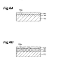
- Fig. 6A is a sectional view schematically showing a compound semiconductor substrate in an electrode forming step
- Fig. 6B is a sectional view schematically showing a compound semiconductor membrane in the electrode forming step.
- Fig. 7 is a graph showing an emission spectrum obtained from a monocrystalline GaN substrate of Experiment Example 5.
- Fig. 8 is a graph showing a correlation between photoluminescence measurement and cathodoluminescence measurement.
- Fig. 9 shows intensities of a peak near 365 nm in respective emission spectra obtained from monocrystalline GaN substrates of Experiment Example 1 to Experiment Example 5.
- Fig. 1 is a flowchart showing steps in a damage evaluation method of a compound semiconductor member and in a production method of a compound semiconductor member according to an embodiment.
- the damage evaluation method of the compound semiconductor member according to the embodiment includes a photoluminescence measurement step S1 and a damage evaluation step S2.
- the production method of the compound semiconductor member according to the embodiment includes the photoluminescence measurement step S1 and damage evaluation step S2 and, preferably, further includes a thin film forming step S3 and an electrode forming step S4.
- FIG. 2 is a drawing schematically showing the photoluminescence measurement step.
- the photoluminescence measurement step S1 is to perform measurement of photoluminescence on a surface 10a of a compound semiconductor substrate 10 (compound semiconductor member).
- the photoluminescence measurement is preferably carried out with a photoluminescence measurement device 16.
- the photoluminescence measurement device 16 has a light source 12 for emitting light L 1 toward the surface 10a of the compound semiconductor substrate 10.
- the energy of light L 1 is set to be higher than the bandgap of the compound semiconductor substrate 10.
- electrons are excited from the valence band to the conduction band and then return to the valence band to emit light L2 from the compound semiconductor substrate 10.
- a light detection unit 14 an emission spectrum is acquired.
- the light L1 is preferably monochromatic laser light, but may include a plurality of wavelength components.
- the light source 12 to be used is preferably a dye laser.
- the light L 1 can be white light containing wavelength components with energy higher than the bandgap of the compound semiconductor substrate 10.
- the compound semiconductor substrate 10 Since the compound semiconductor substrate 10 is a bulk, it will suffer little influence from other members, e.g. influence of the back surface of the compound semiconductor substrate 10 or influence of a jig for fixing the compound semiconductor substrate 10 even if the light L1 penetrates deep, for example, into the interior of the compound semiconductor substrate 10 in the photoluminescence measurement.
- the bandgap of the compound semiconductor substrate 10 is preferably not less than 1.6 x 10 -19 J (1 eV). In this case, even if the compound semiconductor substrate 10 is heated by the light L1 during the photoluminescence measurement, the compound semiconductor substrate 10 will be less likely to be affected by heat. For this reason, the photoluminescence measurement can be performed without difficulty and with high accuracy.
- the compound semiconductor substrate 10 is preferably comprised of a nitride compound semiconductor containing at least one of B, Al, and Ga.
- the compound semiconductor substrate 10 is preferably comprised of an oxide compound semiconductor containing at least one of Be and Zn.
- the compound semiconductor substrate 10 is preferably comprised of a ZnSe compound semiconductor. In all these cases, the bandgap of the compound semiconductor substrate 10 is increased, and thus the compound semiconductor substrate becomes less likely to be affected by heat in the photoluminescence measurement.
- the compound semiconductor substrate 10 is made, for example, of a III-V compound semiconductor such as GaAs or InP, a nitride compound semiconductor such as BN, GaN, AlN, or InN, a II-VI compound semiconductor such as ZnO or ZnS, an oxide compound semiconductor such as Be x O y , ZnO, Ga 2 O 3 , or Al 2 O 3 , a ZnSe compound semiconductor such as ZnSe, or a ternary compound semiconductor such as GaAlN or InGaN.
- III-V compound semiconductor such as GaAs or InP
- a nitride compound semiconductor such as BN, GaN, AlN, or InN
- a II-VI compound semiconductor such as ZnO or ZnS
- an oxide compound semiconductor such as Be x O y , ZnO, Ga 2 O 3 , or Al 2 O 3
- a ZnSe compound semiconductor such as ZnSe
- a ternary compound semiconductor such as GaAl
- the gallium nitride compound semiconductor suitably applicable is of the wurtzite structure or the zinc blende (cubic crystal) structure.
- the surface 10a may be any one of the (0001) face called the C-plane, the (10-10) face called the M-plane, the (11-20) face called the A-plane, the (01-12) face called the R-plane, and the (10-11) face called the S-plane.
- the C-plane can be either a Ga plane consisting of Ga or an N plane consisting of N. Since the Ga plane is normally more resistant to etching, the surface 10a is preferably the Ga plane, but the surface 10a may be the N plane.
- a compound semiconductor membrane 20 (compound semiconductor member) shown in Fig. 3 may also be used instead of the compound semiconductor substrate 10.
- Fig. 3 is a sectional view schematically showing a compound semiconductor membrane provided on a substrate.
- the substrate 22 shown in Fig. 3 is, for example, an amorphous substrate such as a glass substrate, or a monocrystalline substrate such as a sapphire substrate or Si substrate.
- a constituent material of the compound semiconductor membrane 20 can be one of the materials listed for the compound semiconductor substrate 10.
- the photoluminescence measurement is carried out by projecting the light L1 onto a surface 20a of the compound semiconductor membrane 20. If the light L1 is made incident from the direction perpendicular to the surface 20a, the light L2 can contain more information about the substrate 22, depending upon the film thickness of the compound semiconductor membrane 20. As the direction of incidence of the light L1 deviates from the direction perpendicular to the surface 20a, the information about the substrate 22 in the light L2 tends to decrease relatively.
- Fig. 4 is a drawing schematically showing an emission spectrum obtained by the photoluminescence measurement.
- the damage evaluation step S2 is to evaluate damage on the surface 10a of the compound semiconductor substrate 10, using the emission spectrum obtained by the photoluminescence measurement. Examples of such damage include damage, scratches, distortion, or the like due to polishing, etching, or the like.
- the emission spectrum shown in Fig. 4 has a peak P 1 at a wavelength ⁇ 1 corresponding to the bandgap of the compound semiconductor substrate 10.
- the wavelength ⁇ 1 has the same energy as the bandgap.
- the peak P 1 does not always have to be maximum at the wavelength ⁇ 1 .
- This emission spectrum also has a peak P 2 at a wavelength ⁇ 2 located on the longer wavelength side than the wavelength ⁇ 1 .
- the peak P 2 does not always have to be maximum at the wavelength ⁇ 2 .
- the use of this emission spectrum enables detailed evaluation of damage on the surface 10a by Method 1 to Method 4 described below.
- the compound semiconductor substrate 10 is made, for example, of a monocrystalline material or polycrystalline material
- the monocrystalline material or polycrystalline material turns into the amorphous form in a damaged region, and thus it becomes easier to discriminate the damaged region from the other region without damage. For this reason, damage becomes easier to detect, so that the accuracy of damage evaluation can be improved.
- Method 1 is to perform evaluation of damage using the half width W 1 of the peak P 1 .
- Method 1 enables detailed damage evaluation as described below, using the half width W 1 of the peak P 1 .
- the half width W 1 of the peak P 1 varies with change in the spread of the band of the compound semiconductor substrate 10.
- the spread of the band varies with change in the interatomic distance between atoms constituting the compound semiconductor substrate 10.
- the interatomic distance varies depending upon the level of damage on the surface 10a. Therefore, the level of damage can be evaluated in detail by use of the half width W 1 of the peak P 1 .
- the half width W 1 of the peak P 1 tends to increase with increasing level of damage.
- Method 1 is suitably applicable to production of compound semiconductor substrate 10.
- the compound semiconductor substrate 10 is determined to be nondefective when the half width W 1 of the peak P 1 is not more than a predetermined threshold; this permits the compound semiconductor substrate 10 with a low level of damage to be produced at a high yield.
- Method 2 is to perform evaluation of damage using the intensity I 2 of the peak P 2 .
- Method 2 enables detailed damage evaluation as described below, using the intensity I 2 of the peak P 2 .
- the peak P 2 arises from energy levels appearing between bands of the compound semiconductor substrate 10. Therefore, the peak P 2 appears if damage to induce emission of light exists in the compound semiconductor substrate 10. Since the intensity I 2 of the peak P 2 varies depending upon the level of damage to induce emission of light, the level of damage can be evaluated in detail by use of the intensity I 2 of the peak P 2 . For example, the intensity I 2 of the peak P 2 tends to increase with increasing level of damage.
- Method 2 is suitably applicable to production of compound semiconductor substrate 10.
- the compound semiconductor substrate 10 is determined to be nondefective when the intensity I 2 of the peak P 2 is not more than a predetermined threshold, relative to an intensity of a peak located at the wavelength ⁇ 2 in an emission spectrum obtained by photoluminescence measurement on a surface of a compound semiconductor substrate from which damage is preliminarily eliminated; this permits the compound semiconductor substrate 10 with a low level of damage to be produced at a high yield.
- Method 3 is to perform evaluation of damage using the half width W 2 of the peak P 2 .
- Method 3 enables detailed damage evaluation as described below, using the half width W 2 of the peak P 2 .
- the level of damage can be evaluated in detail by use of the half width W 2 of the peak P 2 .
- the half width W 2 of the peak P 2 tends to increase with increasing level of damage.
- Method 3 is suitably applicable to production of compound semiconductor substrate 10.
- the compound semiconductor substrate 10 is determined to be nondefective when the half width W 2 of the peak P 2 is not more than a predetermined threshold; this permits the compound semiconductor substrate 10 with a low level of damage to be produced at a high yield.
- Method 4 is to perform evaluation of damage using an intensity ratio (I 1 /I 2 ) of the intensity I 1 of the peak P 1 to the intensity I 2 of the peak P 2 .
- Method 4 enables detailed damage evaluation as described below, using the intensity ratio (I 1 /I 2 ).
- the intensity ratio (I 1 /I 2 ) can be an index of relationship between the level of damage to change arrangement of atoms constituting the compound semiconductor substrate 10 and the level of damage to induce emission of light. Therefore, the relationship can be evaluated in detail by use of the intensity ratio (I 1 /I 2 ). For example, the intensity ratio (I 1 /I 2 ) tends to decrease with increasing level of damage.
- Method 4 is suitably applicable to production of compound semiconductor substrate 10.
- the compound semiconductor substrate 10 is determined to be nondefective when the intensity ratio (I 1 /I 2 ) is not less than a predetermined threshold; this permits the compound semiconductor substrate 10 with a low level of damage to be produced at a high yield.
- Method 5 is to perform evaluation of damage using the intensity I 1 of the peak P 1 .
- the intensity I 1 of the peak P 1 decreases with increasing level of damage.
- Method 5 is suitably applicable to production of compound semiconductor substrate 10.
- the compound semiconductor substrate 10 is determined to be nondefective when the intensity I 1 of the peak P 1 is not less than a predetermined threshold, relative to an intensity of a peak located at the wavelength ⁇ 1 in an emission spectrum obtained by photoluminescence measurement on a surface of a compound semiconductor substrate from which damage is preliminarily eliminated; this permits the compound semiconductor substrate 10 with a low level of damage to be produced at a high yield.
- the intensity ratio (I 1 /I 2 ) is preferably not less than 2.
- a gallium nitride compound semiconductor substrate is obtained with a low level of damage on its surface.
- the intensity I 1 of the peak P 1 at the wavelength ⁇ 1 (near 365 nm) is preferably not less than 1/10 of an intensity of a peak at the wavelength ⁇ 1 (near 365 nm) in an emission spectrum obtained by photoluminescence measurement on a surface of a gallium nitride compound semiconductor substrate from which damage is eliminated (a gallium nitride compound semiconductor member without damage).
- a gallium nitride compound semiconductor substrate is obtained with a low level of damage on its surface.
- Damage of compound semiconductor membrane 20 may also be evaluated instead of the compound semiconductor substrate 10.
- the photoluminescence measurement is preliminarily carried out on the surface 22a of the substrate 22, and the level of damage can be evaluated in detail on the surface 20a of the compound semiconductor membrane 20 provided on the substrate 22, by one of Method 1 to Method 4. Since the relative influence of damage on the compound semiconductor membrane 20 is greater, the damage can be detected easier even if the level of damage is low.
- the compound semiconductor membrane 20 with a low level of damage can be produced at a high yield by use of Method 1 to Method 5.
- the intensity ratio (I 1 /I 2 ) is preferably not less than 2. In this case, a gallium nitride compound semiconductor membrane is obtained with a low level of damage on its surface.
- the intensity I 1 of the peak P 1 at the wavelength ⁇ 1 (near 365 nm) is preferably not less than 1/10 of an intensity of a peak at the wavelength ⁇ 1 (near 365 nm) in an emission spectrum obtained by photoluminescence measurement on a surface of a gallium nitride compound semiconductor membrane from which damage is eliminated (a gallium nitride compound semiconductor member without damage).
- a gallium nitride compound semiconductor membrane is obtained with a low level of damage on its surface.
- Fig. 5A is a sectional view schematically showing a compound semiconductor substrate in the thin film forming step.
- Fig. 5B is a sectional view schematically showing a compound semiconductor membrane in the thin film forming step.
- the thin film forming step S3 is preferably carried out after the damage evaluation step S2.
- the thin film forming step S3 is to form a thin film 30 on the surface 10a of the compound semiconductor substrate 10, as shown in Fig. 5A.
- the thin film 30 is formed, for example, by an epitaxial growth method.
- the thin film 30 can be a compound semiconductor film, an oxide film, a ZnO film, an amorphous film, or the like.
- an improvement is made in crystallinity and surface roughness of the thin film 30.
- the compound semiconductor substrate 10 is made of a gallium nitride compound semiconductor and where the intensity ratio (I 1 /I 2 ) is not less than 2, an improvement is made in crystallinity and surface roughness of the thin film 30 made of a gallium nitride compound semiconductor.
- the compound semiconductor substrate 10 is made of a gallium nitride compound semiconductor and where the intensity I 1 of the peak P 1 at the wavelength ⁇ 1 (near 365 nm) is not less than 1/10 of an intensity of a peak at the wavelength ⁇ 1 (near 365 nm) in an emission spectrum obtained by photoluminescence measurement on a surface of a gallium nitride compound semiconductor substrate from which damage is eliminated (a gallium nitride compound semiconductor member without damage), an improvement is made in crystallinity and surface roughness of the thin film 30 made of a gallium nitride compound semiconductor.
- the thin film forming step S3 may also be to form a thin film 32 on the surface 20a of the compound semiconductor membrane 20, as shown in Fig. 5B.
- the thin film 32 is formed, for example, by an epitaxial growth method.
- the thin film 32 can be the same as the thin film 30.
- the compound semiconductor membrane 20 is made of a gallium nitride compound semiconductor and where the intensity ratio (I 1 /I 2 ) is not less than 2, an improvement is made in crystallinity and surface roughness of the thin film 32 made of a gallium nitride compound semiconductor.
- the compound semiconductor membrane 20 is made of a gallium nitride compound semiconductor and where the intensity I 1 of the peak P 1 at the wavelength ⁇ 1 (near 365 nm) is not less than 1/10 of an intensity of a peak at the wavelength ⁇ 1 (near 365 nm) in an emission spectrum obtained by photoluminescence measurement on a surface of a gallium nitride compound semiconductor membrane from which damage is eliminated (a gallium nitride compound semiconductor member without damage), an improvement is made in crystallinity and surface roughness of the thin film 32 made of a gallium nitride compound semiconductor.
- Fig. 6A is a sectional view schematically showing a compound semiconductor substrate in the electrode forming step.
- Fig. 6B is a sectional view schematically showing a compound semiconductor membrane in the electrode forming step.
- the electrode forming step S4 is preferably carried out after the damage evaluation step S2 and more preferably carried out after the thin film forming step S3.
- the electrode forming step S4 is to form an electrode 40, for example, of a metal film or the like on the thin film 30, as shown in Fig. 6A.
- the thin film 30 has excellent crystallinity and reduced surface roughness, and occurrence of damage can be suppressed at the interface between the thin film 30 and the electrode 40.
- the electrode 40 may also be formed directly on the surface 10a of the compound semiconductor substrate 10. In that case, when the compound semiconductor substrate 10 with a low level of damage is used, occurrence of damage can be suppressed at the interface between the compound semiconductor substrate 10 and the electrode 40.
- the electrode forming step S4 may also be to form an electrode 42 on the thin film 32, as shown in Fig. 6B.
- the thin film 32 has excellent crystallinity and reduced surface roughness, and occurrence of damage can be suppressed at the interface between the thin film 32 and the electrode 42.
- the electrode 40 may also be formed directly on the surface 20a of the compound semiconductor membrane 20. In that case, when the compound semiconductor membrane 20 with a low level of damage is used, occurrence of damage can be suppressed at the interface between the compound semiconductor membrane 20 and the electrode 42.
- a compound semiconductor device can be produced through the steps described above.
- Example 1 First, a monocrystalline GaN ingot was sliced to prepare a monocrystalline GaN substrate with the diameter of 2 inches. The surface of the monocrystalline GaN substrate prepared was polished and thereafter the surface was dry-etched by reactive ion etching (RIE). The conditions for dry etching were as follows.
- the monocrystalline GaN substrate was immersed in a 5% NH 4 OH solution at 40°C for 15 minutes to effect wet etching.
- the monocrystalline GaN substrate of Experiment Example 1 was obtained as described above.
- Example 2 First, a monocrystalline GaN ingot was sliced to prepare a monocrystalline GaN substrate with the diameter of 2 inches. The surface of the monocrystalline GaN substrate prepared was roughly polished and thereafter the surface was further polished by means of diamond abrasive grains with the grain size of 0.5 ⁇ m. Thereafter, the surface was cleaned with isopropyl alcohol. The monocrystalline GaN substrate of Experiment Example 2 was obtained as described above.
- Example 3 A monocrystalline GaN substrate of Experiment Example 3 was obtained in the same manner as in Experiment Example 2 except that diamond abrasive grains with the grain size of 0.1 ⁇ m were used instead of the diamond abrasive grains with the grain size of 0.5 ⁇ m.
- Example 4 A monocrystalline GaN substrate of Experiment Example 4 was obtained by effecting dry etching in Experiment Example 1 on a monocrystalline GaN substrate obtained in the same manner as in Experiment Example 3.
- Example 5 A monocrystalline GaN substrate of Experiment Example 5 was obtained by effecting wet etching with a diluted H 3 PO 4 solution on a monocrystalline GaN substrate obtained in the same manner as in Experiment Example 4.
- the photoluminescence measurement was conducted using a He-Cd laser that can emit a laser beam with the wavelength of 325 nm, as the light source 12.
- the laser beam is made incident normally to the surfaces of the monocrystalline GaN substrates of Experiment Example 1 to Experiment Example 5, to obtain their respective emission spectra.
- Fig. 7 shows an example of an emission spectrum.
- Fig. 7 is a graph showing the emission spectrum obtained from the monocrystalline GaN substrate of Experiment Example 5.
- the vertical axis indicates the PL intensities (photoluminescence intensities) and the horizontal axis the wavelengths.
- the PL intensities are relative values with respect to 1 for the intensity I 1 of the peak P 1 near 365 nm.
- a broad peak P 2 appears near 470-640 nm on the longer wavelength side than 365 nm.
- the photoluminescence measurement was carried out at wavelength intervals of 0.5 nm and values near the peak P 1 were interpolated by a Gaussian distribution.
- the background was adjusted by linear approximation of wing portions of the peak P 1 .
- Fig. 8 is a graph showing a correlation between photoluminescence measurement and cathodoluminescence measurement.
- the vertical axis indicates the PL intensities and the horizontal axis the CL intensities (cathodoluminescence intensities).
- plot D1 to plot D5 represent respective intensities I 1 of the peak P 1 near 365 nm in the emission spectra obtained from the monocrystalline GaN substrates of Experiment Example 1 to Experiment Example 5.
- the PL intensities are relative values with respect to 1 for the intensity I 1 of the peak P 1 near 365 nm in the emission spectrum obtained from the monocrystalline GaN substrate of Experiment Example 2.
- the CL intensities are also relative values with respect to 1 for the CL intensity in the monocrystalline GaN substrate of Experiment Example 2.
- Fig. 9 shows the intensities I 1 of the peak P 1 near 365 nm in the emission spectra obtained from the monocrystalline GaN substrates of Experiment Example 1 to Experiment Example 5. It is seen from Fig. 9 that the level of damage on the surface increases in the order of Experiment Example 1, Experiment Example 4, Experiment Example 5, Experiment Example 3, and Experiment Example 2.
- Table 1 shows the half width W 1 of the peak P 1 near 365 nm in each of the emission spectra obtained from the monocrystalline GaN substrates of Experiment Example 1 to Experiment Example 5. It is seen from Table 1 that the half width W 1 of the peak P 1 increases with increasing level of damage.
- Table 2 shows the intensity I 2 and half width W 2 of the peak P 2 in each of the emission spectra obtained from the monocrystalline GaN substrates of Experiment Example 1 to Experiment Example 5. It is seen from Table 2 that the intensity I 2 and half width W 2 of the peak P 2 both increase with increasing level of damage.
- Table 3 shows the intensity ratio (I 1 /I 2 ) in each of the emission spectra obtained from the monocrystalline GaN substrates of Experiment Example 1 to Experiment Example 5. It is seen from Table 3 that the intensity ratio (I 1 /I 2 ) decreases with increasing level of damage.
- Example 6 A monocrystalline GaN substrate of Experiment Example 6 without damage was obtained in the same manner as in Experiment Example 1, except that the substrate used was a monocrystalline GaN substrate 20 mm square.
- Example 7 A monocrystalline GaN ingot was sliced to prepare a monocrystalline GaN substrate 20 mm square. The surface of the monocrystalline GaN substrate prepared was roughly polished and thereafter the surface was further polished by means of diamond abrasive grains with the grain size of 0.3 ⁇ m, to obtain the monocrystalline GaN substrate of Experiment Example 7.
- Example 8 A monocrystalline GaN substrate of Experiment Example 8 was obtained in the same manner as in Experiment Example 7 except that diamond abrasive grains with the grain size of 0.8 ⁇ m were used instead of the diamond abrasive grains with the grain size of 0.3 ⁇ m.
- Table 4 shows the intensity I 1 of the peak P 1 and the intensity ratio (I 1 /I 2 ) in each of the emission spectra obtained from the monocrystalline GaN substrates of Experiment Example 6 to Experiment Example 8. It is seen from the intensity I 1 of the peak P 1 that the level of damage on the surface increases in the order of Experiment Example 6, Experiment Example 7, and Experiment Example 8. Therefore, it is seen that the intensity ratio (I 1 /I 2 ) decreases with increasing level of damage.
- GaN a thin film of GaN was formed in the thickness of 1 ⁇ m by HVPE on the surfaces of the monocrystalline GaN substrates of Experiment Example 6 to Experiment Example 8.
- the conditions for formation of the GaN thin film are presented below.
- GaCl gas is obtained by reaction of Ga metal with HCl gas at 880°C.
- the present invention provides the damage evaluation methods of the compound semiconductor member permitting the detailed evaluation of the level of damage on the surface and the production methods of the compound semiconductor member with a low level of damage, and also provides the gallium nitride compound semiconductor members and gallium nitride compound semiconductor membranes with a low level of damage.
Landscapes
- Health & Medical Sciences (AREA)
- Physics & Mathematics (AREA)
- General Physics & Mathematics (AREA)
- Immunology (AREA)
- Analytical Chemistry (AREA)
- Biochemistry (AREA)
- General Health & Medical Sciences (AREA)
- Chemical & Material Sciences (AREA)
- Life Sciences & Earth Sciences (AREA)
- Pathology (AREA)
- Nuclear Medicine, Radiotherapy & Molecular Imaging (AREA)
- Condensed Matter Physics & Semiconductors (AREA)
- Electromagnetism (AREA)
- Optics & Photonics (AREA)
- Testing Or Measuring Of Semiconductors Or The Like (AREA)
- Led Devices (AREA)
- Semiconductor Lasers (AREA)
- Investigating, Analyzing Materials By Fluorescence Or Luminescence (AREA)
Abstract
Description
- The present invention relates to a damage evaluation method of a compound semiconductor member, a production method of a compound semiconductor member, a gallium nitride compound semiconductor member, and a gallium nitride compound semiconductor membrane.
- Compound semiconductors have various merits in comparison with Si. For example, the compound semiconductors permit control of the bandgap through adjustment of compositions. Furthermore, the compound semiconductors have such optical properties as direct transition and wide bandgap, and are thus suitably applied to optical devices such as LEDs or LDs. Since the compound semiconductors have high carrier mobility, they are also suitably applied to high-speed devices.
- In producing such compound semiconductor devices as the optical devices or high-speed devices, a substrate used is a compound semiconductor substrate, or a laminated substrate in which a compound semiconductor membrane is formed on an amorphous substrate such as a glass substrate. For example, a compound semiconductor membrane or electrodes are formed on a surface of the compound semiconductor substrate or laminated substrate. The device characteristics of the compound semiconductor devices are significantly affected by an interface between the compound semiconductor substrate or laminated substrate and the compound semiconductor membrane or by interfaces between the compound semiconductor substrate or laminated substrate and the electrodes. Therefore, it is important to evaluate the interfaces in the compound semiconductor devices.
- In production of the compound semiconductor devices, damage occurs on the foregoing interfaces in several production processes. For example, since surface roughness of the compound semiconductor substrate or laminated substrate affects the device characteristics, the surface of the compound semiconductor substrate or laminated substrate is subjected to polishing or etching. This process produces scratches or distortion on the surface to cause damage on the surface. For example, dry etching or wet etching or the like is used in forming a thin film or fine pattern of nanometer size on the surface of the compound semiconductor substrate or laminated substrate. At this time, damage is caused on the surface of the compound semiconductor substrate or laminated substrate or on the surface of the thin film or fine pattern.
- When a compound semiconductor device is produced, for example, by growing an epitaxial film on the surface of the compound semiconductor substrate or compound semiconductor membrane with the surface including the damage as described above, the device characteristics are degraded by virtue of the damage existing at the interface between the compound semiconductor substrate or compound semiconductor membrane and the epitaxial film.
- Methods for evaluating the damage on the surface of the compound semiconductor substrate or compound semiconductor membrane include methods using X-ray diffraction, scanning electron microscope (SEM), cathodoluminescence, or the like as usually adopted methods.
- On the other hand,
Japanese Patent Application Laid-Open No. 9-246341 - However, the method disclosed in the foregoing Patent Application is not always satisfactory for performing detailed evaluation of a level of damage.
- An object of the present invention is therefore to provide a damage evaluation method of a compound semiconductor member permitting detailed evaluation of a level of damage on a surface and a production method of a compound semiconductor member with a low level of damage, and to provide a gallium nitride compound semiconductor member and a gallium nitride compound semiconductor membrane with a low level of damage.
- In order to solve the above problem, a damage evaluation method of a compound semiconductor member according to the present invention is a method of evaluating damage of a compound semiconductor member, comprising: a step of performing measurement of photoluminescence on a surface of the compound semiconductor member; and a step of evaluating damage on the surface of the compound semiconductor member, using a half width of a peak at a wavelength corresponding to a bandgap of the compound semiconductor member, in an emission spectrum obtained by the measurement of photoluminescence.
- The damage evaluation method of the compound semiconductor member according to the present invention enables detailed damage evaluation, using the half width of the peak at the wavelength corresponding to the bandgap (which will be referred to hereinafter as "first peak").
- The interatomic distance between atoms constituting the compound semiconductor member varies according to the level of damage. The variation in the interatomic distance results in also changing the spread of the band. Furthermore, the change in the spread of the band leads to change in the half width of the first peak. Therefore, the half width of the first peak can be used for detailed evaluation of a level of damage. For example, the half width of the first peak tends to increase with increasing level of damage.
- Another damage evaluation method of a compound semiconductor member according to the present invention is a method of evaluating damage of a compound semiconductor member, comprising: a step of performing measurement of photoluminescence on a surface of the compound semiconductor member; and a step of evaluating damage on the surface of the compound semiconductor member, using an intensity of a peak located on a longer wavelength side than a wavelength corresponding to a bandgap of the compound semiconductor member, in an emission spectrum obtained by the measurement of photoluminescence.
- The damage evaluation method of the compound semiconductor member according to the present invention permits detailed damage evaluation, using the intensity of the peak located on the longer wavelength side than the wavelength corresponding to the bandgap (which will be referred to hereinafter as "second peak").
- The second peak arises from energy levels appearing between bands of the compound semiconductor member. The intensity of the second peak varies according to the level of damage to induce emission of light, and thus the level of damage can be evaluated in detail by use of the intensity of the second peak. For example, the intensity of the second peak tends to increase with increasing level of damage.
- Another damage evaluation method of a compound semiconductor member according to the present invention is a method of evaluating damage of a compound semiconductor member, comprising: a step of performing measurement of photoluminescence on a surface of the compound semiconductor member; and a step of evaluating damage on the surface of the compound semiconductor member, using a half width of a peak located on a longer wavelength side than a wavelength corresponding to a bandgap of the compound semiconductor member, in an emission spectrum obtained by the measurement of photoluminescence.
- The damage evaluation method of the compound semiconductor member according to the present invention permits detailed damage evaluation, using the half width of the second peak.
- Since the half width of the second peak varies according to the level of damage to induce emission of light, the level of damage can be evaluated in detail by use of the half width of the second peak. For example, the half width of the second peak tends to increase with increasing level of damage.
- Another damage evaluation method of a compound semiconductor member according to the present invention is a method of evaluating damage of a compound semiconductor member, comprising: a step of performing measurement of photoluminescence on a surface of the compound semiconductor member; and a step of evaluating damage on the surface of the compound semiconductor member, using a ratio of an intensity of a peak at a wavelength corresponding to a bandgap of the compound semiconductor member to an intensity of a peak located on a longer wavelength side than the wavelength corresponding to the bandgap, in an emission spectrum obtained by the measurement of photoluminescence.
- The damage evaluation method of the compound semiconductor member according to the present invention permits detailed damage evaluation, using the intensity ratio of the intensity of the first peak to the intensity of the second peak.
- The use of the intensity ratio enables us to minutely evaluate the relationship between levels of damage to change the arrangement of atoms constituting the compound semiconductor member, and levels of damage to induce emission of light. For example, the intensity ratio tends to decrease with increasing level of damage.
- The compound semiconductor member is preferably a compound semiconductor substrate. In this case, it is feasible to evaluate the level of damage on the surface of the compound semiconductor substrate. Even in a case where light penetrates deep, for example, into the interior of the compound semiconductor member in the photoluminescence measurement, there is little influence from other members, such as influence of the back surface of the compound semiconductor member, influence of a jig for fixing the compound semiconductor member, and so on.
- The compound semiconductor member is preferably a compound semiconductor membrane provided on a substrate. In this case, by preliminarily performing the photoluminescence measurement on the surface of the substrate, it becomes feasible to evaluate a level of damage on the surface of the compound semiconductor membrane provided on the substrate. Even if the level of damage is low, relative influence of damage on the compound semiconductor membrane will be large, so that the damage can be easier to detect.
- The compound semiconductor member is preferably comprised of either one of monocrystalline material and polycrystalline material. In this case, the monocrystalline material or polycrystalline material turns into an amorphous form in a damaged region, and it thus becomes easier to discriminate the damaged region from the other region without damage. For this reason, the damage becomes easier to detect, and thus an improvement is made in the accuracy of damage evaluation.
- The bandgap is preferably not less than 1.6 x 10⁻¹⁹ J. In this case, the compound semiconductor member is less likely to be affected by heat during the photoluminescence measurement. For this reason, the photoluminescence measurement becomes easier.
- The compound semiconductor member is preferably comprised of a nitride compound semiconductor containing at least one of B, Al, and Ga. The compound semiconductor member is preferably comprised of an oxide compound semiconductor containing at least one of Be and Zn. Furthermore, the compound semiconductor member is preferably comprised of a ZnSe compound semiconductor.
- A production method of a compound semiconductor member according to the present invention is a method of producing a compound semiconductor member, comprising: a step of performing measurement of photoluminescence on a surface of the compound semiconductor member; and a step of determining that the compound semiconductor member is nondefective when a half width of a peak at a wavelength corresponding to a bandgap of the compound semiconductor member in an emission spectrum obtained by the measurement of photoluminescence is not more than a predetermined threshold.
- The production method of the compound semiconductor member according to the present invention enables detailed evaluation of a level of damage, using the half width of the first peak. For this reason, the production method of the compound semiconductor member according to the present invention can be used to produce the compound semiconductor member with a low level of damage.
- Another production method of a compound semiconductor member according to the present invention is a method of producing a compound semiconductor member, comprising: a step of performing measurement of photoluminescence on a surface of the compound semiconductor member; and a step of determining that the compound semiconductor member is nondefective when an intensity of a peak at a wavelength corresponding to a bandgap of the compound semiconductor member in an emission spectrum obtained by the measurement of photoluminescence is not less than a predetermined threshold with respect to an intensity of a peak at the wavelength in an emission spectrum obtained by measurement of photoluminescence on a surface of a compound semiconductor member without damage.
- The production method of the compound semiconductor member of the present invention enables evaluation of the level of damage, based on the comparison between the intensities of the peaks at the wavelength corresponding to the bandgap. For this reason, the production method of the compound semiconductor member according to the present invention can be used to produce the compound semiconductor member with a low level of damage.
- Another production method of a compound semiconductor member according to the present invention is a method of producing a compound semiconductor member, comprising: a step of performing measurement of photoluminescence on a surface of the compound semiconductor member; and a step of determining that the compound semiconductor member is nondefective when a half width of a peak on a longer wavelength side than a wavelength corresponding to a bandgap of the compound semiconductor member in an emission spectrum obtained by the measurement of photoluminescence is not more than a predetermined threshold.
- The production method of the compound semiconductor member according to the present invention enables detailed evaluation of the level of damage, using the intensity of the second peak. For this reason, the production method of the compound semiconductor member according to the present invention can be used to produce the compound semiconductor member with a low level of damage.
- Another production method of a compound semiconductor member according to the present invention is a method of producing a compound semiconductor member, comprising: a step of performing measurement of photoluminescence on a surface of the compound semiconductor member; and a step of determining that the compound semiconductor member is nondefective when a ratio of an intensity of a peak at a wavelength corresponding to a bandgap of the compound semiconductor member to an intensity of a peak located on a longer wavelength side than the wavelength corresponding to the bandgap in an emission spectrum obtained by the measurement of photoluminescence is not less than a predetermined threshold.
- The production method of the compound semiconductor member according to the present invention enables detailed evaluation of the level of damage, using the intensity ratio of the intensity of the first peak to the intensity of the second peak. For this reason, the production method of the compound semiconductor member according to the present invention can be used to produce the compound semiconductor member with a low level of damage.
- The compound semiconductor member is preferably a compound semiconductor substrate. In this case, it is feasible to produce the compound semiconductor substrate with a low level of damage.
- The compound semiconductor member is preferably a compound semiconductor membrane provided on a substrate. In this case, it is feasible to form the compound semiconductor membrane with a low level of damage on the substrate.
- The production methods of the compound semiconductor member preferably further comprise a step of forming a thin film on the surface of the compound semiconductor member, after the step of determining that the compound semiconductor member is nondefective. In this case, since the thin film is formed on the surface of the compound semiconductor member with a low level of damage, crystallinity and surface roughness of the thin film are improved.
- The production methods of the compound semiconductor member preferably further comprise a step of forming an electrode on the surface of the compound semiconductor member, after the step of determining that the compound semiconductor member is nondefective. In this case, the electrode can be formed on the surface of the compound semiconductor member with a low level of damage.
- A gallium nitride compound semiconductor member according to the present invention is a gallium nitride compound semiconductor member wherein in an emission spectrum obtained by measurement of photoluminescence on a surface of the gallium nitride compound semiconductor member, an intensity of a peak at a wavelength corresponding to a bandgap of the gallium nitride compound semiconductor member is not less than twice an intensity of a peak located on a longer wavelength side than the wavelength corresponding to the bandgap.
- Another gallium nitride compound semiconductor member according to the present invention is a gallium nitride compound semiconductor member wherein in an emission spectrum obtained by measurement of photoluminescence on a surface of the gallium nitride compound semiconductor member, an intensity of a peak at a wavelength corresponding to a bandgap of the gallium nitride compound semiconductor member is not less than 1/10 of an intensity of a peak at the wavelength in an emission spectrum obtained by measurement of photoluminescence on a surface of a gallium nitride compound semiconductor member without damage.
- In the gallium nitride compound semiconductor members of the present invention, the level of damage on the surface is low.
- The gallium nitride compound semiconductor member is preferably a gallium nitride compound semiconductor substrate. In this gallium nitride compound semiconductor substrate, the level of damage on the surface is low.
- The gallium nitride compound semiconductor member is preferably a gallium nitride compound semiconductor membrane provided on a substrate. In this gallium nitride compound semiconductor membrane, the level of damage on the surface is low.
- A gallium nitride compound semiconductor membrane according to the present invention is a gallium nitride compound semiconductor membrane formed on a gallium nitride compound semiconductor member wherein in an emission spectrum obtained by measurement of photoluminescence on a surface of the gallium nitride compound semiconductor member, an intensity of a peak at a wavelength corresponding to a bandgap of the gallium nitride compound semiconductor member is not less than twice an intensity of a peak located on a longer wavelength side than the wavelength corresponding to the bandgap.
- Another gallium nitride compound semiconductor membrane according to the present invention is a gallium nitride compound semiconductor membrane formed on a gallium nitride compound semiconductor member wherein in an emission spectrum obtained by measurement of photoluminescence on a surface of the gallium nitride compound semiconductor member, an intensity of a peak at a wavelength corresponding to a bandgap of the gallium nitride compound semiconductor member is not less than 1/10 of an intensity of a peak at the wavelength in an emission spectrum obtained by measurement of photoluminescence on a surface of a gallium nitride compound semiconductor member without damage.
- The gallium nitride compound semiconductor membrane of the present invention is formed on the gallium nitride compound semiconductor member with a low level of damage on the surface. For this reason, the gallium nitride compound semiconductor membrane is improved in crystallinity and surface roughness.
- Fig. 1 is a flowchart showing steps in a damage evaluation method of a compound semiconductor member and in a production method of a compound semiconductor member according to an embodiment.
- Fig. 2 is a drawing schematically showing a photoluminescence measurement step.
- Fig. 3 is a sectional view schematically showing a compound semiconductor membrane provided on a substrate.
- Fig. 4 is a drawing schematically showing an emission spectrum obtained by photoluminescence measurement.
- Fig. 5A is a sectional view schematically showing a compound semiconductor substrate in a thin film forming step, and Fig. 5B is a sectional view schematically showing a compound semiconductor membrane in the thin film forming step.
- Fig. 6A is a sectional view schematically showing a compound semiconductor substrate in an electrode forming step, and Fig. 6B is a sectional view schematically showing a compound semiconductor membrane in the electrode forming step.
- Fig. 7 is a graph showing an emission spectrum obtained from a monocrystalline GaN substrate of Experiment Example 5.
- Fig. 8 is a graph showing a correlation between photoluminescence measurement and cathodoluminescence measurement.
- Fig. 9 shows intensities of a peak near 365 nm in respective emission spectra obtained from monocrystalline GaN substrates of Experiment Example 1 to Experiment Example 5.
- Embodiments of the present invention will be described below in detail with reference to the accompanying drawings. In the description of the drawings identical or equivalent elements will be denoted by the same reference symbols, without redundant description.
- Fig. 1 is a flowchart showing steps in a damage evaluation method of a compound semiconductor member and in a production method of a compound semiconductor member according to an embodiment. The damage evaluation method of the compound semiconductor member according to the embodiment includes a photoluminescence measurement step S1 and a damage evaluation step S2. The production method of the compound semiconductor member according to the embodiment includes the photoluminescence measurement step S1 and damage evaluation step S2 and, preferably, further includes a thin film forming step S3 and an electrode forming step S4.
- (Photoluminescence Measurement Step)
Fig. 2 is a drawing schematically showing the photoluminescence measurement step. The photoluminescence measurement step S1 is to perform measurement of photoluminescence on asurface 10a of a compound semiconductor substrate 10 (compound semiconductor member). The photoluminescence measurement is preferably carried out with aphotoluminescence measurement device 16. - The
photoluminescence measurement device 16 has alight source 12 for emittinglight L 1 toward thesurface 10a of thecompound semiconductor substrate 10. The energy oflight L 1 is set to be higher than the bandgap of thecompound semiconductor substrate 10. As the light L1 impinges on thesurface 10a, electrons are excited from the valence band to the conduction band and then return to the valence band to emit light L2 from thecompound semiconductor substrate 10. When the light L2 enters alight detection unit 14, an emission spectrum is acquired. - The light L1 is preferably monochromatic laser light, but may include a plurality of wavelength components. For obtaining the
light L 1 containing a plurality of wavelength components, thelight source 12 to be used is preferably a dye laser. Thelight L 1 can be white light containing wavelength components with energy higher than the bandgap of thecompound semiconductor substrate 10. - Since the
compound semiconductor substrate 10 is a bulk, it will suffer little influence from other members, e.g. influence of the back surface of thecompound semiconductor substrate 10 or influence of a jig for fixing thecompound semiconductor substrate 10 even if the light L1 penetrates deep, for example, into the interior of thecompound semiconductor substrate 10 in the photoluminescence measurement. - The bandgap of the
compound semiconductor substrate 10 is preferably not less than 1.6 x 10⁻¹⁹ J (1 eV). In this case, even if thecompound semiconductor substrate 10 is heated by the light L1 during the photoluminescence measurement, thecompound semiconductor substrate 10 will be less likely to be affected by heat. For this reason, the photoluminescence measurement can be performed without difficulty and with high accuracy. - The
compound semiconductor substrate 10 is preferably comprised of a nitride compound semiconductor containing at least one of B, Al, and Ga. Thecompound semiconductor substrate 10 is preferably comprised of an oxide compound semiconductor containing at least one of Be and Zn. Furthermore, thecompound semiconductor substrate 10 is preferably comprised of a ZnSe compound semiconductor. In all these cases, the bandgap of thecompound semiconductor substrate 10 is increased, and thus the compound semiconductor substrate becomes less likely to be affected by heat in the photoluminescence measurement. - More specifically, the
compound semiconductor substrate 10 is made, for example, of a III-V compound semiconductor such as GaAs or InP, a nitride compound semiconductor such as BN, GaN, AlN, or InN, a II-VI compound semiconductor such as ZnO or ZnS, an oxide compound semiconductor such as BexOy, ZnO, Ga2O3, or Al2O3, a ZnSe compound semiconductor such as ZnSe, or a ternary compound semiconductor such as GaAlN or InGaN. These compound semiconductors may be doped with an impurity. - For example, in a case where the
compound semiconductor substrate 10 is made of a gallium nitride compound semiconductor, the gallium nitride compound semiconductor suitably applicable is of the wurtzite structure or the zinc blende (cubic crystal) structure. In the case of the wurtzite structure, thesurface 10a may be any one of the (0001) face called the C-plane, the (10-10) face called the M-plane, the (11-20) face called the A-plane, the (01-12) face called the R-plane, and the (10-11) face called the S-plane. The C-plane can be either a Ga plane consisting of Ga or an N plane consisting of N. Since the Ga plane is normally more resistant to etching, thesurface 10a is preferably the Ga plane, but thesurface 10a may be the N plane. - In performing the photoluminescence measurement, a compound semiconductor membrane 20 (compound semiconductor member) shown in Fig. 3 may also be used instead of the
compound semiconductor substrate 10. - Fig. 3 is a sectional view schematically showing a compound semiconductor membrane provided on a substrate. The
substrate 22 shown in Fig. 3 is, for example, an amorphous substrate such as a glass substrate, or a monocrystalline substrate such as a sapphire substrate or Si substrate. A constituent material of thecompound semiconductor membrane 20 can be one of the materials listed for thecompound semiconductor substrate 10. - In this case, the photoluminescence measurement is carried out by projecting the light L1 onto a
surface 20a of thecompound semiconductor membrane 20. If the light L1 is made incident from the direction perpendicular to thesurface 20a, the light L2 can contain more information about thesubstrate 22, depending upon the film thickness of thecompound semiconductor membrane 20. As the direction of incidence of the light L1 deviates from the direction perpendicular to thesurface 20a, the information about thesubstrate 22 in the light L2 tends to decrease relatively. - (Damage Evaluation Step)
Fig. 4 is a drawing schematically showing an emission spectrum obtained by the photoluminescence measurement. The damage evaluation step S2 is to evaluate damage on thesurface 10a of thecompound semiconductor substrate 10, using the emission spectrum obtained by the photoluminescence measurement. Examples of such damage include damage, scratches, distortion, or the like due to polishing, etching, or the like. - The emission spectrum shown in Fig. 4 has a peak P1 at a wavelength λ1 corresponding to the bandgap of the
compound semiconductor substrate 10. The wavelength λ1 has the same energy as the bandgap. The peak P1 does not always have to be maximum at the wavelength λ1. This emission spectrum also has a peak P2 at a wavelength λ2 located on the longer wavelength side than the wavelength λ1. The peak P2 does not always have to be maximum at the wavelength λ2. The use of this emission spectrum enables detailed evaluation of damage on thesurface 10a byMethod 1 toMethod 4 described below. - When the
compound semiconductor substrate 10 is made, for example, of a monocrystalline material or polycrystalline material, the monocrystalline material or polycrystalline material turns into the amorphous form in a damaged region, and thus it becomes easier to discriminate the damaged region from the other region without damage. For this reason, damage becomes easier to detect, so that the accuracy of damage evaluation can be improved. - <
Method 1>
Method 1 is to perform evaluation of damage using the half width W1 of the peak P1. Method 1 enables detailed damage evaluation as described below, using the half width W1 of the peak P1. - The half width W1 of the peak P1 varies with change in the spread of the band of the
compound semiconductor substrate 10. Here the spread of the band varies with change in the interatomic distance between atoms constituting thecompound semiconductor substrate 10. The interatomic distance varies depending upon the level of damage on thesurface 10a. Therefore, the level of damage can be evaluated in detail by use of the half width W1 of the peak P1. For example, the half width W1 of the peak P1 tends to increase with increasing level of damage. -
Method 1 is suitably applicable to production ofcompound semiconductor substrate 10. Thecompound semiconductor substrate 10 is determined to be nondefective when the half width W1 of the peak P1 is not more than a predetermined threshold; this permits thecompound semiconductor substrate 10 with a low level of damage to be produced at a high yield. - <
Method 2>
Method 2 is to perform evaluation of damage using the intensity I2 of the peak P2. Method 2 enables detailed damage evaluation as described below, using the intensity I2 of the peak P2. - The peak P2 arises from energy levels appearing between bands of the
compound semiconductor substrate 10. Therefore, the peak P2 appears if damage to induce emission of light exists in thecompound semiconductor substrate 10. Since the intensity I2 of the peak P2 varies depending upon the level of damage to induce emission of light, the level of damage can be evaluated in detail by use of the intensity I2 of the peak P2. For example, the intensity I2 of the peak P2 tends to increase with increasing level of damage. -
Method 2 is suitably applicable to production ofcompound semiconductor substrate 10. Thecompound semiconductor substrate 10 is determined to be nondefective when the intensity I2 of the peak P2 is not more than a predetermined threshold, relative to an intensity of a peak located at the wavelength λ2 in an emission spectrum obtained by photoluminescence measurement on a surface of a compound semiconductor substrate from which damage is preliminarily eliminated; this permits thecompound semiconductor substrate 10 with a low level of damage to be produced at a high yield. - <
Method 3>
Method 3 is to perform evaluation of damage using the half width W2 of the peak P2. Method 3 enables detailed damage evaluation as described below, using the half width W2 of the peak P2. - Since the half width W2 of the peak P2 varies according to the level of damage to induce emission of light, the level of damage can be evaluated in detail by use of the half width W2 of the peak P2. For example, the half width W2 of the peak P2 tends to increase with increasing level of damage.
-
Method 3 is suitably applicable to production ofcompound semiconductor substrate 10. Thecompound semiconductor substrate 10 is determined to be nondefective when the half width W2 of the peak P2 is not more than a predetermined threshold; this permits thecompound semiconductor substrate 10 with a low level of damage to be produced at a high yield. - <
Method 4>
Method 4 is to perform evaluation of damage using an intensity ratio (I1/I2) of the intensity I1 of the peak P1 to the intensity I2 of the peak P2. Method 4 enables detailed damage evaluation as described below, using the intensity ratio (I1/I2). - The intensity ratio (I1/I2) can be an index of relationship between the level of damage to change arrangement of atoms constituting the
compound semiconductor substrate 10 and the level of damage to induce emission of light. Therefore, the relationship can be evaluated in detail by use of the intensity ratio (I1/I2). For example, the intensity ratio (I1/I2) tends to decrease with increasing level of damage. -
Method 4 is suitably applicable to production ofcompound semiconductor substrate 10. Thecompound semiconductor substrate 10 is determined to be nondefective when the intensity ratio (I1/I2) is not less than a predetermined threshold; this permits thecompound semiconductor substrate 10 with a low level of damage to be produced at a high yield. - <
Method 5>
Method 5 is to perform evaluation of damage using the intensity I1 of the peak P1. For example, the intensity I1 of the peak P1 decreases with increasing level of damage.Method 5 is suitably applicable to production ofcompound semiconductor substrate 10. Thecompound semiconductor substrate 10 is determined to be nondefective when the intensity I1 of the peak P1 is not less than a predetermined threshold, relative to an intensity of a peak located at the wavelength λ1 in an emission spectrum obtained by photoluminescence measurement on a surface of a compound semiconductor substrate from which damage is preliminarily eliminated; this permits thecompound semiconductor substrate 10 with a low level of damage to be produced at a high yield. - When the
compound semiconductor substrate 10 is made, for example, of a gallium nitride compound semiconductor, the intensity ratio (I1/I2) is preferably not less than 2. In this case, a gallium nitride compound semiconductor substrate is obtained with a low level of damage on its surface. - When the
compound semiconductor substrate 10 is made, for example, of a gallium nitride compound semiconductor, the intensity I1 of the peak P1 at the wavelength λ1 (near 365 nm) is preferably not less than 1/10 of an intensity of a peak at the wavelength λ1 (near 365 nm) in an emission spectrum obtained by photoluminescence measurement on a surface of a gallium nitride compound semiconductor substrate from which damage is eliminated (a gallium nitride compound semiconductor member without damage). In this case, a gallium nitride compound semiconductor substrate is obtained with a low level of damage on its surface. - Damage of
compound semiconductor membrane 20 may also be evaluated instead of thecompound semiconductor substrate 10. In this case, the photoluminescence measurement is preliminarily carried out on thesurface 22a of thesubstrate 22, and the level of damage can be evaluated in detail on thesurface 20a of thecompound semiconductor membrane 20 provided on thesubstrate 22, by one ofMethod 1 toMethod 4. Since the relative influence of damage on thecompound semiconductor membrane 20 is greater, the damage can be detected easier even if the level of damage is low. - Furthermore, the
compound semiconductor membrane 20 with a low level of damage can be produced at a high yield by use ofMethod 1 toMethod 5. When thecompound semiconductor membrane 20 is made, for example, of a gallium nitride compound semiconductor, the intensity ratio (I1/I2) is preferably not less than 2. In this case, a gallium nitride compound semiconductor membrane is obtained with a low level of damage on its surface. - When the
compound semiconductor membrane 20 is made, for example, of a gallium nitride compound semiconductor, the intensity I1 of the peak P1 at the wavelength λ1 (near 365 nm) is preferably not less than 1/10 of an intensity of a peak at the wavelength λ1 (near 365 nm) in an emission spectrum obtained by photoluminescence measurement on a surface of a gallium nitride compound semiconductor membrane from which damage is eliminated (a gallium nitride compound semiconductor member without damage). In this case, a gallium nitride compound semiconductor membrane is obtained with a low level of damage on its surface. - (Thin Film Forming Step)
Fig. 5A is a sectional view schematically showing a compound semiconductor substrate in the thin film forming step. Fig. 5B is a sectional view schematically showing a compound semiconductor membrane in the thin film forming step. The thin film forming step S3 is preferably carried out after the damage evaluation step S2. - The thin film forming step S3 is to form a
thin film 30 on thesurface 10a of thecompound semiconductor substrate 10, as shown in Fig. 5A. Thethin film 30 is formed, for example, by an epitaxial growth method. Thethin film 30 can be a compound semiconductor film, an oxide film, a ZnO film, an amorphous film, or the like. When thethin film 30 is formed on thesurface 10a of thecompound semiconductor substrate 10 with a low level of damage, an improvement is made in crystallinity and surface roughness of thethin film 30. For example, in a case where thecompound semiconductor substrate 10 is made of a gallium nitride compound semiconductor and where the intensity ratio (I1/I2) is not less than 2, an improvement is made in crystallinity and surface roughness of thethin film 30 made of a gallium nitride compound semiconductor. - In addition, for example, in a case where the
compound semiconductor substrate 10 is made of a gallium nitride compound semiconductor and where the intensity I1 of the peak P1 at the wavelength λ1 (near 365 nm) is not less than 1/10 of an intensity of a peak at the wavelength λ1 (near 365 nm) in an emission spectrum obtained by photoluminescence measurement on a surface of a gallium nitride compound semiconductor substrate from which damage is eliminated (a gallium nitride compound semiconductor member without damage), an improvement is made in crystallinity and surface roughness of thethin film 30 made of a gallium nitride compound semiconductor. - The thin film forming step S3 may also be to form a thin film 32 on the
surface 20a of thecompound semiconductor membrane 20, as shown in Fig. 5B. The thin film 32 is formed, for example, by an epitaxial growth method. The thin film 32 can be the same as thethin film 30. When the thin film 32 is formed on thesurface 20a of thecompound semiconductor membrane 20 with a low level of damage, an improvement is made in crystallinity and surface roughness of the thin film 32. For example, in a case where thecompound semiconductor membrane 20 is made of a gallium nitride compound semiconductor and where the intensity ratio (I1/I2) is not less than 2, an improvement is made in crystallinity and surface roughness of the thin film 32 made of a gallium nitride compound semiconductor. - In addition, for example, in a case where the
compound semiconductor membrane 20 is made of a gallium nitride compound semiconductor and where the intensity I1 of the peak P1 at the wavelength λ1 (near 365 nm) is not less than 1/10 of an intensity of a peak at the wavelength λ1 (near 365 nm) in an emission spectrum obtained by photoluminescence measurement on a surface of a gallium nitride compound semiconductor membrane from which damage is eliminated (a gallium nitride compound semiconductor member without damage), an improvement is made in crystallinity and surface roughness of the thin film 32 made of a gallium nitride compound semiconductor. - (Electrode Forming Step)
Fig. 6A is a sectional view schematically showing a compound semiconductor substrate in the electrode forming step. Fig. 6B is a sectional view schematically showing a compound semiconductor membrane in the electrode forming step. The electrode forming step S4 is preferably carried out after the damage evaluation step S2 and more preferably carried out after the thin film forming step S3. - The electrode forming step S4 is to form an
electrode 40, for example, of a metal film or the like on thethin film 30, as shown in Fig. 6A. In this case, thethin film 30 has excellent crystallinity and reduced surface roughness, and occurrence of damage can be suppressed at the interface between thethin film 30 and theelectrode 40. - The
electrode 40 may also be formed directly on thesurface 10a of thecompound semiconductor substrate 10. In that case, when thecompound semiconductor substrate 10 with a low level of damage is used, occurrence of damage can be suppressed at the interface between thecompound semiconductor substrate 10 and theelectrode 40. - The electrode forming step S4 may also be to form an
electrode 42 on the thin film 32, as shown in Fig. 6B. In this case, the thin film 32 has excellent crystallinity and reduced surface roughness, and occurrence of damage can be suppressed at the interface between the thin film 32 and theelectrode 42. - The
electrode 40 may also be formed directly on thesurface 20a of thecompound semiconductor membrane 20. In that case, when thecompound semiconductor membrane 20 with a low level of damage is used, occurrence of damage can be suppressed at the interface between thecompound semiconductor membrane 20 and theelectrode 42. - A compound semiconductor device can be produced through the steps described above.
- The preferred embodiments of the present invention were described above in detail, but it is noted that the present invention is not limited to the above embodiments.
- Subsequently, Experiment Examples associated with the above embodiments will be described.
- (Experiment Example 1)
First, a monocrystalline GaN ingot was sliced to prepare a monocrystalline GaN substrate with the diameter of 2 inches. The surface of the monocrystalline GaN substrate prepared was polished and thereafter the surface was dry-etched by reactive ion etching (RIE).
The conditions for dry etching were as follows. - · Etching gas: Ar gas
- · Supplied power: 200 W
- · Pressure in chamber: 1.3 Pa (10 mTorr)
- · Etching time: 10 minutes
- Thereafter, in order to eliminate damage from the surface, the monocrystalline GaN substrate was immersed in a 5% NH4OH solution at 40°C for 15 minutes to effect wet etching. The monocrystalline GaN substrate of Experiment Example 1 was obtained as described above.
- (Experiment Example 2)
First, a monocrystalline GaN ingot was sliced to prepare a monocrystalline GaN substrate with the diameter of 2 inches. The surface of the monocrystalline GaN substrate prepared was roughly polished and thereafter the surface was further polished by means of diamond abrasive grains with the grain size of 0.5 µm. Thereafter, the surface was cleaned with isopropyl alcohol. The monocrystalline GaN substrate of Experiment Example 2 was obtained as described above. - (Experiment Example 3)
A monocrystalline GaN substrate of Experiment Example 3 was obtained in the same manner as in Experiment Example 2 except that diamond abrasive grains with the grain size of 0.1 µm were used instead of the diamond abrasive grains with the grain size of 0.5 µm. - (Experiment Example 4)
A monocrystalline GaN substrate of Experiment Example 4 was obtained by effecting dry etching in Experiment Example 1 on a monocrystalline GaN substrate obtained in the same manner as in Experiment Example 3. - (Experiment Example 5)
A monocrystalline GaN substrate of Experiment Example 5 was obtained by effecting wet etching with a diluted H3PO4 solution on a monocrystalline GaN substrate obtained in the same manner as in Experiment Example 4. - (Photoluminescence Measurement)
The photoluminescence measurement was conducted using a He-Cd laser that can emit a laser beam with the wavelength of 325 nm, as thelight source 12. The laser beam is made incident normally to the surfaces of the monocrystalline GaN substrates of Experiment Example 1 to Experiment Example 5, to obtain their respective emission spectra. Fig. 7 shows an example of an emission spectrum. - Fig. 7 is a graph showing the emission spectrum obtained from the monocrystalline GaN substrate of Experiment Example 5. The vertical axis indicates the PL intensities (photoluminescence intensities) and the horizontal axis the wavelengths. In Fig. 7 the PL intensities are relative values with respect to 1 for the intensity I1 of the peak P1 near 365 nm. A broad peak P2 appears near 470-640 nm on the longer wavelength side than 365 nm.
- The photoluminescence measurement was carried out at wavelength intervals of 0.5 nm and values near the peak P1 were interpolated by a Gaussian distribution. The background was adjusted by linear approximation of wing portions of the peak P1.
- (Evaluation of Damage)
Fig. 8 is a graph showing a correlation between photoluminescence measurement and cathodoluminescence measurement. The vertical axis indicates the PL intensities and the horizontal axis the CL intensities (cathodoluminescence intensities). In Fig. 8, plot D1 to plot D5 represent respective intensities I1 of the peak P1 near 365 nm in the emission spectra obtained from the monocrystalline GaN substrates of Experiment Example 1 to Experiment Example 5. The PL intensities are relative values with respect to 1 for the intensity I1 of the peak P1 near 365 nm in the emission spectrum obtained from the monocrystalline GaN substrate of Experiment Example 2. The CL intensities are also relative values with respect to 1 for the CL intensity in the monocrystalline GaN substrate of Experiment Example 2. - It is seen from Fig. 8 that there is a correlation between the photoluminescence measurement and the cathodoluminescence measurement. In general, the CL intensity decreases with increasing level of damage, and it is thus seen that the PL intensity also decreases with increasing level of damage.
- Fig. 9 shows the intensities I1 of the peak P1 near 365 nm in the emission spectra obtained from the monocrystalline GaN substrates of Experiment Example 1 to Experiment Example 5. It is seen from Fig. 9 that the level of damage on the surface increases in the order of Experiment Example 1, Experiment Example 4, Experiment Example 5, Experiment Example 3, and Experiment Example 2.
- Table 1 shows the half width W1 of the peak P1 near 365 nm in each of the emission spectra obtained from the monocrystalline GaN substrates of Experiment Example 1 to Experiment Example 5. It is seen from Table 1 that the half width W1 of the peak P1 increases with increasing level of damage.
-
TABLE 1 Half Width W1 of Peak P1[nm] Experiment Example 2 10.6 Experiment Example 3 9.7 Experiment Example 5 8.4 Experiment Example 4 8.1 Experiment Example 1 7.1 - Table 2 shows the intensity I2 and half width W2 of the peak P2 in each of the emission spectra obtained from the monocrystalline GaN substrates of Experiment Example 1 to Experiment Example 5. It is seen from Table 2 that the intensity I2 and half width W2 of the peak P2 both increase with increasing level of damage.
-
TABLE 2 Intensity I2 of Peak P2 Half Width W2 of Peak P2[nm] Experiment Example 2 1 142 Experiment Example 3 0.86 137 Experiment Example 5 0.31 134 Experiment Example 4 0.25 105 Experiment Example 1 0.11 101 - Table 3 shows the intensity ratio (I1/I2) in each of the emission spectra obtained from the monocrystalline GaN substrates of Experiment Example 1 to Experiment Example 5. It is seen from Table 3 that the intensity ratio (I1/I2) decreases with increasing level of damage.
-
TABLE 3 Intensity Ratio (I1/I2) Experiment Example 2 1 Experiment Example 3 4 Experiment Example 5 19 Experiment Example 4 28 Experiment Example 1 100 - (Experiment Example 6)
A monocrystalline GaN substrate of Experiment Example 6 without damage was obtained in the same manner as in Experiment Example 1, except that the substrate used was amonocrystalline GaN substrate 20 mm square. - (Experiment Example 7)
A monocrystalline GaN ingot was sliced to prepare amonocrystalline GaN substrate 20 mm square. The surface of the monocrystalline GaN substrate prepared was roughly polished and thereafter the surface was further polished by means of diamond abrasive grains with the grain size of 0.3 µm, to obtain the monocrystalline GaN substrate of Experiment Example 7. - (Experiment Example 8)
A monocrystalline GaN substrate of Experiment Example 8 was obtained in the same manner as in Experiment Example 7 except that diamond abrasive grains with the grain size of 0.8 µm were used instead of the diamond abrasive grains with the grain size of 0.3 µm. - The photoluminescence measurement was carried out on the surfaces of the monocrystalline GaN substrates of Experiment Example 6 to Experiment Example 8. Table 4 shows the intensity I1 of the peak P1 and the intensity ratio (I1/I2) in each of the emission spectra obtained from the monocrystalline GaN substrates of Experiment Example 6 to Experiment Example 8. It is seen from the intensity I1 of the peak P1 that the level of damage on the surface increases in the order of Experiment Example 6, Experiment Example 7, and Experiment Example 8. Therefore, it is seen that the intensity ratio (I1/I2) decreases with increasing level of damage.
-
TABLE 4 Intensity I1 of Peak P1 Intensity Ratio (I1/I2) Experiment Example 6 1 102 Experiment Example 7 0.31 2.4 Experiment Example 8 0.09 1 - Next, a thin film of GaN was formed in the thickness of 1 µm by HVPE on the surfaces of the monocrystalline GaN substrates of Experiment Example 6 to Experiment Example 8. The conditions for formation of the GaN thin film are presented below. GaCl gas is obtained by reaction of Ga metal with HCl gas at 880°C.
- · Temperature of monocrystalline GaN substrate: 1000°C
- · Reaction gases: NH3 gas and GaCl gas
- · Pressure of NH3 gas: 10 kPa
- · Pressure of GaCl gas: 0.6 Pa
- After the thin film of GaN was formed, surface roughness of the GaN thin film (Ra: arithmetic mean roughness) was measured by AFM. A percentage of lattice strain to the bulk was measured by X-ray diffraction. Table 5 shows the measurement results of these. It was seen from Table 5 that the monocrystalline GaN substrates of Experiment Example 6 and Experiment Example 7 had satisfactory performance as substrates to be used for the compound semiconductor devices.
-
TABLE 5 Arithmetic Mean Roughness[nm] Percentage of Lattice Strain[%] Experiment Example 6 0.82 0.01 Experiment Example 7 0.99 0.05 Experiment Example 8 1.61 0.17 - The present invention provides the damage evaluation methods of the compound semiconductor member permitting the detailed evaluation of the level of damage on the surface and the production methods of the compound semiconductor member with a low level of damage, and also provides the gallium nitride compound semiconductor members and gallium nitride compound semiconductor membranes with a low level of damage.
Claims (25)
- A method of evaluating damage of a compound semiconductor member, comprising:a step of performing measurement of photoluminescence on a surface of the compound semiconductor member; anda step of evaluating damage on the surface of the compound semiconductor member, using a half width of a peak at a wavelength corresponding to a bandgap of the compound semiconductor member, in an emission spectrum obtained by the measurement of photoluminescence.
- A method of evaluating damage of a compound semiconductor member, comprising:a step of performing measurement of photoluminescence on a surface of the compound semiconductor member; anda step of evaluating damage on the surface of the compound semiconductor member, using an intensity of a peak located on a longer wavelength side than a wavelength corresponding to a bandgap of the compound semiconductor member, in an emission spectrum obtained by the measurement of photoluminescence.
- A method of evaluating damage of a compound semiconductor member, comprising:a step of performing measurement of photoluminescence on a surface of the compound semiconductor member; anda step of evaluating damage on the surface of the compound semiconductor member, using a half width of a peak located on a longer wavelength side than a wavelength corresponding to a bandgap of the compound semiconductor member, in an emission spectrum obtained by the measurement of photoluminescence.
- A method of evaluating damage of a compound semiconductor member, comprising:a step of performing measurement of photoluminescence on a surface of the compound semiconductor member; anda step of evaluating damage on the surface of the compound semiconductor member, using a ratio of an intensity of a peak at a wavelength corresponding to a bandgap of the compound semiconductor member to an intensity of a peak located on a longer wavelength side than the wavelength corresponding to the bandgap, in an emission spectrum obtained by the measurement of photoluminescence.
- The damage evaluation method of the compound semiconductor member according to any one of Claims 1 to 4, wherein the compound semiconductor member is a compound semiconductor substrate.
- The damage evaluation method of the compound semiconductor member according to any one of Claims 1 to 4, wherein the compound semiconductor member is a compound semiconductor membrane provided on a substrate.
- The damage evaluation method of the compound semiconductor member according to any one of Claims 1 to 6, wherein the compound semiconductor member is comprised of either one of monocrystalline material and polycrystalline material.
- The damage evaluation method of the compound semiconductor member according to any one of Claims 1 to 7, wherein the bandgap is not less than 1.6 x 10⁻¹⁹ J.
- The damage evaluation method of the compound semiconductor member according to any one of Claims 1 to 8, wherein the compound semiconductor member is comprised of a nitride compound semiconductor containing at least one of B, Al, and Ga.
- The damage evaluation method of the compound semiconductor member according to any one of Claims 1 to 8, wherein the compound semiconductor member is comprised of an oxide compound semiconductor containing at least one of Be and Zn.
- The damage evaluation method of the compound semiconductor member according to any one of Claims 1 to 8, wherein the compound semiconductor member is comprised of a ZnSe compound semiconductor.
- A method of producing a compound semiconductor member, comprising:a step of performing measurement of photoluminescence on a surface of the compound semiconductor member; anda step of determining that the compound semiconductor member is nondefective when a half width of a peak at a wavelength corresponding to a bandgap of the compound semiconductor member in an emission spectrum obtained by the measurement of photoluminescence is not more than a predetermined threshold.
- A method of producing a compound semiconductor member, comprising:a step of performing measurement of photoluminescence on a surface of the compound semiconductor member; anda step of determining that the compound semiconductor member is nondefective when an intensity of a peak at a wavelength corresponding to a bandgap of the compound semiconductor member in an emission spectrum obtained by the measurement of photoluminescence is not less than a predetermined threshold with respect to an intensity of a peak at the wavelength in an emission spectrum obtained by measurement of photoluminescence on a surface of a compound semiconductor member without damage.
- A method of producing a compound semiconductor member, comprising:a step of performing measurement of photoluminescence on a surface of the compound semiconductor member; anda step of determining that the compound semiconductor member is nondefective when a half width of a peak on a longer wavelength side than a wavelength corresponding to a bandgap of the compound semiconductor member in an emission spectrum obtained by the measurement of photoluminescence is not more than a predetermined threshold.
- A method of producing a compound semiconductor member, comprising:a step of performing measurement of photoluminescence on a surface of the compound semiconductor member; anda step of determining that the compound semiconductor member is nondefective when a ratio of an intensity of a peak at a wavelength corresponding to a bandgap of the compound semiconductor member to an intensity of a peak located on a longer wavelength side than the wavelength corresponding to the bandgap in an emission spectrum obtained by the measurement of photoluminescence is not less than a predetermined threshold.
- The production method of the compound semiconductor member according to any one of Claims 12 to 15, wherein the compound semiconductor member is a compound semiconductor substrate.
- The production method of the compound semiconductor member according to any one of Claims 12 to 15, wherein the compound semiconductor member is a compound semiconductor membrane provided on a substrate.
- The production method of the compound semiconductor member according to any one of Claims 12 to 17, further comprising a step of forming a thin film on the surface of the compound semiconductor member, after the step of determining that the compound semiconductor member is nondefective.
- The production method according to any one of Claims 12 to 18, further comprising a step of forming an electrode on the surface of the compound semiconductor member, after a step of determining that the compound semiconductor member is nondefective.
- A gallium nitride compound semiconductor member wherein in an emission spectrum obtained by measurement of photoluminescence on a surface of the gallium nitride compound semiconductor member, an intensity of a peak at a wavelength corresponding to a bandgap of the gallium nitride compound semiconductor member is not less than twice an intensity of a peak located on a longer wavelength side than the wavelength corresponding to the bandgap.
- A gallium nitride compound semiconductor member wherein in an emission spectrum obtained by measurement of photoluminescence on a surface of the gallium nitride compound semiconductor member, an intensity of a peak at a wavelength corresponding to a bandgap of the gallium nitride compound semiconductor member is not less than 1/10 of an intensity of a peak at the wavelength in an emission spectrum obtained by measurement of photoluminescence on a surface of a gallium nitride compound semiconductor member without damage.
- The gallium nitride compound semiconductor member according to Claim 20 or 21, wherein the gallium nitride compound semiconductor member is a gallium nitride compound semiconductor substrate.
- The gallium nitride compound semiconductor member according to Claim 20 or 21, wherein the gallium nitride compound semiconductor member is a gallium nitride compound semiconductor membrane provided on a substrate.
- A gallium nitride compound semiconductor membrane formed on a gallium nitride compound semiconductor member wherein in an emission spectrum obtained by measurement of photoluminescence on a surface of the gallium nitride compound semiconductor member, an intensity of a peak at a wavelength corresponding to a bandgap of the gallium nitride compound semiconductor member is not less than twice an intensity of a peak located on a longer wavelength side than the wavelength corresponding to the bandgap.
- A gallium nitride compound semiconductor membrane formed on a gallium nitride compound semiconductor member wherein in an emission spectrum obtained by measurement of photoluminescence on a surface of the gallium nitride compound semiconductor member, an intensity of a peak at a wavelength corresponding to a bandgap of the gallium nitride compound semiconductor member is not less than 1/10 of an intensity of a peak at the wavelength in an emission spectrum obtained by measurement of photoluminescence on a surface of a gallium nitride compound semiconductor member without damage.
Applications Claiming Priority (1)
| Application Number | Priority Date | Filing Date | Title |
|---|---|---|---|
| JP2005165957A JP2006339605A (en) | 2005-06-06 | 2005-06-06 | Damage evaluation method for compound semiconductor member, method for producing compound semiconductor member, gallium nitride compound semiconductor member, and gallium nitride compound semiconductor film |
Publications (2)
| Publication Number | Publication Date |
|---|---|
| EP1731897A2 true EP1731897A2 (en) | 2006-12-13 |
| EP1731897A3 EP1731897A3 (en) | 2009-07-22 |
Family
ID=36930361
Family Applications (1)
| Application Number | Title | Priority Date | Filing Date |
|---|---|---|---|
| EP06009693A Withdrawn EP1731897A3 (en) | 2005-06-06 | 2006-05-10 | Damage evaluation method and production method of compound semiconductor member |
Country Status (6)
| Country | Link |
|---|---|
| US (2) | US20060272573A1 (en) |
| EP (1) | EP1731897A3 (en) |
| JP (1) | JP2006339605A (en) |
| KR (1) | KR20060127752A (en) |
| CN (1) | CN1877805B (en) |
| TW (1) | TW200707613A (en) |
Cited By (1)
| Publication number | Priority date | Publication date | Assignee | Title |
|---|---|---|---|---|
| EP2680058A1 (en) * | 2012-06-27 | 2014-01-01 | Samsung Corning Precision Materials Co., Ltd. | Apparatus for measuring quality of gallium nitride |
Families Citing this family (15)
| Publication number | Priority date | Publication date | Assignee | Title |
|---|---|---|---|---|
| JP2006339605A (en) * | 2005-06-06 | 2006-12-14 | Sumitomo Electric Ind Ltd | Damage evaluation method for compound semiconductor member, method for producing compound semiconductor member, gallium nitride compound semiconductor member, and gallium nitride compound semiconductor film |
| KR101172364B1 (en) * | 2006-11-02 | 2012-08-08 | 삼성코닝정밀소재 주식회사 | GaN SINGLE-CRYSTAL SUBSTRATE AND METHOD FOR PROCESSING SURFACES OF GaN SINGLE-CRYSTAL SUBSTRATE |
| CN102569557A (en) * | 2007-07-17 | 2012-07-11 | 住友电气工业株式会社 | Method for manufacturing electronic device, method for manufacturing epitaxial substrate, iii nitride semiconductor element and gallium nitride epitaxial substrate |
| JP4935591B2 (en) * | 2007-09-11 | 2012-05-23 | 住友電気工業株式会社 | Method for fabricating group III nitride semiconductor optical device and method for measuring photoluminescence spectrum |
| JP5575372B2 (en) * | 2008-03-04 | 2014-08-20 | 日立金属株式会社 | Gallium nitride substrate |
| JP2011103400A (en) * | 2009-11-11 | 2011-05-26 | Sumitomo Electric Ind Ltd | Compound semiconductor element |
| JP5416650B2 (en) * | 2010-05-10 | 2014-02-12 | 日立金属株式会社 | Gallium nitride substrate |
| JP2013010681A (en) * | 2011-05-31 | 2013-01-17 | Hitachi Cable Ltd | Gallium nitride substrate, light emitting element, field effect transistor, and method for producing epitaxial film |
| JP6204036B2 (en) | 2012-03-16 | 2017-09-27 | 株式会社神戸製鋼所 | Evaluation method of oxide semiconductor thin film and quality control method of oxide semiconductor thin film |
| JP6696729B2 (en) * | 2015-03-18 | 2020-05-20 | 株式会社Sumco | Semiconductor substrate evaluation method and semiconductor substrate manufacturing method |
| CN111355118B (en) * | 2018-12-20 | 2021-07-20 | 中科芯电半导体科技(北京)有限公司 | VCSEL structure epitaxial material structure for photoluminescence test and preparation method |
| JP7232074B2 (en) * | 2019-02-19 | 2023-03-02 | 住友化学株式会社 | III-nitride semiconductor device and etching device |
| CN110544643B (en) * | 2019-09-11 | 2022-06-28 | 东方日升(常州)新能源有限公司 | A method for quickly judging the burn-through depth of metal paste without damage |
| WO2024042777A1 (en) * | 2022-08-26 | 2024-02-29 | 日本碍子株式会社 | Method for inspecting group-iii element nitride substrate, method for producing group-iii element nitride substrate, and method for producing semiconductor element |
| JPWO2024252461A1 (en) * | 2023-06-05 | 2024-12-12 |
Family Cites Families (21)
| Publication number | Priority date | Publication date | Assignee | Title |
|---|---|---|---|---|
| JPS5860550A (en) * | 1981-10-07 | 1983-04-11 | Agency Of Ind Science & Technol | Measuring method for density of impurities in epitaxial silicon crystal |
| JP2654454B2 (en) * | 1988-04-29 | 1997-09-17 | 豊田合成株式会社 | Dry etching method for semiconductor |
| JPH031553A (en) * | 1989-05-30 | 1991-01-08 | Hikari Gijutsu Kenkyu Kaihatsu Kk | Measuring method and apparatus for semiconductor |
| US5602418A (en) * | 1992-08-07 | 1997-02-11 | Asahi Kasei Kogyo Kabushiki Kaisha | Nitride based semiconductor device and manufacture thereof |
| US5679152A (en) * | 1994-01-27 | 1997-10-21 | Advanced Technology Materials, Inc. | Method of making a single crystals Ga*N article |
| JP3124209B2 (en) * | 1994-06-30 | 2001-01-15 | シャープ株式会社 | Method for manufacturing compound semiconductor crystal layer |
| JPH098356A (en) * | 1995-06-16 | 1997-01-10 | Sumitomo Chem Co Ltd | Method for manufacturing electrode for 3-5 group compound semiconductor |
| GB2306640B (en) * | 1995-10-17 | 1998-01-14 | Toshiba Cambridge Res Center | Method of characterising a semiconductor material |
| JP2003133246A (en) * | 1996-01-19 | 2003-05-09 | Matsushita Electric Ind Co Ltd | Gallium nitride based compound semiconductor light emitting device and method of manufacturing gallium nitride based compound semiconductor |
| JPH09246341A (en) * | 1996-03-12 | 1997-09-19 | Nippon Steel Corp | Sample for damage evaluation of semiconductor wafer and damage evaluation method using this sample |
| JP2001085737A (en) * | 1999-09-10 | 2001-03-30 | Sharp Corp | Nitride semiconductor light emitting device |
| US7189358B2 (en) * | 2000-08-08 | 2007-03-13 | California Institute Of Technology | Integrated micropump analysis chip and method of making the same |
| US6579068B2 (en) * | 2000-08-09 | 2003-06-17 | California Institute Of Technology | Method of manufacture of a suspended nitride membrane and a microperistaltic pump using the same |
| US6647796B2 (en) * | 2000-08-11 | 2003-11-18 | California Institue Of Technology | Semiconductor nitride pressure microsensor and method of making and using the same |
| US6780239B2 (en) * | 2000-10-19 | 2004-08-24 | Ricoh Company, Ltd. | Crystal growth method, crystal growth apparatus, group-III nitride crystal and group-III nitride semiconductor device |
| EP1378949A4 (en) * | 2001-03-21 | 2006-03-22 | Mitsubishi Cable Ind Ltd | Semiconductor light-emitting device |
| EP1942531B1 (en) * | 2002-02-15 | 2010-05-19 | Mitsubishi Chemical Corporation | Light emitting device and illuminator using the same |
| JP3878868B2 (en) * | 2002-03-01 | 2007-02-07 | シャープ株式会社 | GaN-based laser element |
| CN101188344A (en) * | 2002-03-08 | 2008-05-28 | 松下电器产业株式会社 | Semiconductor laser and its manufacturing method |
| JP4206086B2 (en) * | 2004-08-03 | 2009-01-07 | 住友電気工業株式会社 | Nitride semiconductor light emitting device and method for manufacturing nitride semiconductor light emitting device |
| JP2006339605A (en) * | 2005-06-06 | 2006-12-14 | Sumitomo Electric Ind Ltd | Damage evaluation method for compound semiconductor member, method for producing compound semiconductor member, gallium nitride compound semiconductor member, and gallium nitride compound semiconductor film |
-
2005
- 2005-06-06 JP JP2005165957A patent/JP2006339605A/en not_active Withdrawn
-
2006
- 2006-05-05 TW TW095115992A patent/TW200707613A/en unknown
- 2006-05-10 EP EP06009693A patent/EP1731897A3/en not_active Withdrawn
- 2006-05-30 KR KR1020060049078A patent/KR20060127752A/en not_active Withdrawn
- 2006-06-01 CN CN2006100887044A patent/CN1877805B/en not_active Expired - Fee Related
- 2006-06-06 US US11/446,976 patent/US20060272573A1/en not_active Abandoned
-
2007
- 2007-10-11 US US11/907,322 patent/US8177911B2/en active Active
Non-Patent Citations (1)
| Title |
|---|
| None * |
Cited By (1)
| Publication number | Priority date | Publication date | Assignee | Title |
|---|---|---|---|---|
| EP2680058A1 (en) * | 2012-06-27 | 2014-01-01 | Samsung Corning Precision Materials Co., Ltd. | Apparatus for measuring quality of gallium nitride |
Also Published As
| Publication number | Publication date |
|---|---|
| US8177911B2 (en) | 2012-05-15 |
| KR20060127752A (en) | 2006-12-13 |
| JP2006339605A (en) | 2006-12-14 |
| US20060272573A1 (en) | 2006-12-07 |
| CN1877805A (en) | 2006-12-13 |
| EP1731897A3 (en) | 2009-07-22 |
| US20080044338A1 (en) | 2008-02-21 |
| TW200707613A (en) | 2007-02-16 |
| CN1877805B (en) | 2010-04-21 |
Similar Documents
| Publication | Publication Date | Title |
|---|---|---|
| US8177911B2 (en) | Damage evaluation method of compound semiconductor member, production method of compound semiconductor member, gallium nitride compound semiconductor member and gallium nitride compound semiconductor membrane | |
| US8115927B2 (en) | Production method of compound semiconductor member | |
| EP1736574B1 (en) | Nitride crystal, epilayer-containing nitride crystal substrate, semiconductor device and method of manufacturing the same | |
| JP5493861B2 (en) | Method for manufacturing group III nitride crystal substrate | |
| US7125801B2 (en) | Method of manufacturing Group III nitride crystal substrate, etchant used in the method, Group III nitride crystal substrate, and semiconductor device including the same | |
| EP2199436A1 (en) | Gan epitaxial substrate, semiconductor device and methods for manufacturing gan epitaxial substrate and semiconductor device | |
| EP1176231A2 (en) | A boride-based substrate for growing semiconducting layers thereon and a semiconductor device using the same | |
| JP4525309B2 (en) | Method for evaluating group III-V nitride semiconductor substrate | |
| KR20150052275A (en) | A group iii-v substrate material with particular crystallographic features and methods of making | |
| JP2010118668A (en) | Damage evaluation method of compound semiconductor element member, production method of compound semiconductor element member, gallium nitride based compound semiconductor member, and gallium nitride based compound semiconductor film | |
| JP5304715B2 (en) | Group III-V nitride semiconductor substrate | |
| Klein | Establishing a Two Step FACELO Process in HVPE | |
| HK1095212A (en) | Damage evaluation method of compound semiconductor member |
Legal Events
| Date | Code | Title | Description |
|---|---|---|---|
| PUAI | Public reference made under article 153(3) epc to a published international application that has entered the european phase |
Free format text: ORIGINAL CODE: 0009012 |
|
| AK | Designated contracting states |
Kind code of ref document: A2 Designated state(s): AT BE BG CH CY CZ DE DK EE ES FI FR GB GR HU IE IS IT LI LT LU LV MC NL PL PT RO SE SI SK TR |
|
| AX | Request for extension of the european patent |
Extension state: AL BA HR MK YU |
|
| PUAL | Search report despatched |
Free format text: ORIGINAL CODE: 0009013 |
|
| AK | Designated contracting states |
Kind code of ref document: A3 Designated state(s): AT BE BG CH CY CZ DE DK EE ES FI FR GB GR HU IE IS IT LI LT LU LV MC NL PL PT RO SE SI SK TR |
|
| AX | Request for extension of the european patent |
Extension state: AL BA HR MK YU |
|
| 17P | Request for examination filed |
Effective date: 20090929 |
|
| 17Q | First examination report despatched |
Effective date: 20091102 |
|
| AKX | Designation fees paid |
Designated state(s): DE FR GB |
|
| STAA | Information on the status of an ep patent application or granted ep patent |
Free format text: STATUS: THE APPLICATION IS DEEMED TO BE WITHDRAWN |
|
| 18D | Application deemed to be withdrawn |
Effective date: 20190219 |