EP1730575B1 - Electrowetting display element - Google Patents
Electrowetting display element Download PDFInfo
- Publication number
- EP1730575B1 EP1730575B1 EP05729449A EP05729449A EP1730575B1 EP 1730575 B1 EP1730575 B1 EP 1730575B1 EP 05729449 A EP05729449 A EP 05729449A EP 05729449 A EP05729449 A EP 05729449A EP 1730575 B1 EP1730575 B1 EP 1730575B1
- Authority
- EP
- European Patent Office
- Prior art keywords
- liquid
- layer
- upper layer
- conductive
- particles
- Prior art date
- Legal status (The legal status is an assumption and is not a legal conclusion. Google has not performed a legal analysis and makes no representation as to the accuracy of the status listed.)
- Expired - Fee Related
Links
Images

Classifications
-
- G—PHYSICS
- G02—OPTICS
- G02B—OPTICAL ELEMENTS, SYSTEMS OR APPARATUS
- G02B26/00—Optical devices or arrangements for the control of light using movable or deformable optical elements
- G02B26/004—Optical devices or arrangements for the control of light using movable or deformable optical elements based on a displacement or a deformation of a fluid
- G02B26/005—Optical devices or arrangements for the control of light using movable or deformable optical elements based on a displacement or a deformation of a fluid based on electrowetting
-
- B—PERFORMING OPERATIONS; TRANSPORTING
- B82—NANOTECHNOLOGY
- B82Y—SPECIFIC USES OR APPLICATIONS OF NANOSTRUCTURES; MEASUREMENT OR ANALYSIS OF NANOSTRUCTURES; MANUFACTURE OR TREATMENT OF NANOSTRUCTURES
- B82Y30/00—Nanotechnology for materials or surface science, e.g. nanocomposites
Definitions
- This invention relates to the field of display elements, in particular to the field of passive display elements.
- Display elements can be either active, i.e. emit light such as LED, OLED, PLED, EL, or passive, i.e. affect the passage, reflection or refraction of light such as LCD, CLC, e-ink etc..
- Some passive systems are bistable such they can be switched and remain switched after the power has been removed.
- Most configurations previously disclosed can be readily adapted to colour functionality.
- US6473492 discloses a fluid element device that rearranges fluid within a capillary tube. A voltage is used to move the fluid within the capillary to a desired level.
- US2002/0080920 discloses a filter device using an array of elements based upon US6473492 for use with X-ray imaging equipment.
- US2003/0085850 discloses an electrostatic device that changes a meniscus shape such that the focal length of the device changes.
- US6449081 describes a focussing element based on the electrowetting phenomenon.
- WO2/002099527 describes a display element with a defined prismatic structure that contains two immiscible fluids together with electrodes such that the fluid can be rearranged with the cell.
- the display element is capacitative in nature and thus has low power consumption and is switched by low voltages.
- the element modifies the reflectivity of the surface thereof.
- a display element comprising at least two porous layers, a conductive liquid residing in the upper layer, the liquid having a contact angle with the material of the upper layer of less than about 60°, the material of the lower layer being conductive and insulated from the liquid with a dielectric covering, the liquid having a contact angle with the material of the lower layer of greater than about 90°, whereby on application of a voltage between the lower layer and the liquid the liquid moves out of the upper layer into the lower layer thereby effecting an optical change in the upper layer.
- the invention further provides a display device comprising at least one element as described above including means for connection of each element to a circuit to create a matrix display.
- the present invention is simple to manufacture over large areas because of the stochastic structure of the elements and may be manufactured via roll-to-roll techniques. It fulfils the requirement of capturing small liquid elements by capillarity. However the switching time of the element is not limited by its area. It is also simple to address and drive, via suitably patterned passive or active matrix type backplanes.
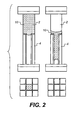
- Figure 1 is a schematic view of a display element according to the invention.
- the invention relates to a passive display element.
- upper defines the side from which an element would be viewed.
- lower defines the side opposite the upper side.
- upper and lower are not to be taken as limiting the orientation of the element according to the invention.
- the element is based upon a two layer porous system.
- the upper layer 2 and lower layer 4 are sandwiched between an upper conductor 12 and a lower conductor 14.
- the upper conductor 12 should be transparent.
- the conductor may equally be formed of, for example, wire filaments in which case the material does not have to be transparent. It will be understood by those skilled in the art that it is not necessary for the conductors to be at the top and bottom of the element. What is required is that a voltage can be applied to a liquid 10.
- the conductors may be at the side of the element or at any other suitable location.
- An insulating layer 16 is located between the lower layer 4 and the lower conductor 14.
- the element is encapsulated by an upper substrate 26 and a lower substrate 28.
- the substrates should be insulating and impermeable to liquid.
- the upper substrate must be of a transparent material.
- the upper layer 2 comprises a plurality of particles 6, such as silica.
- silica is only an example of the material which can be used. Any other lyophilic material may be used that can be matched with the refractive index of the liquid used.
- the particle sizes would be in the order of 30nm to 2 microns.
- a liquid 10 resides in the pore space of the upper layer 2.
- the liquid may be water but it will be understood by those skilled in the art that it is not essential that the liquid is water. However the liquid must be conductive.
- the conductive liquid may be created by adding ions to a solvent. Alternatively the conductive liquid may be an ionic liquid.
- the refractive index of the particles 6 in the upper layer 2 should be substantially the same as the refractive index of the liquid 10.
- the size of the particles 6 should be a substantial fraction of the wavelength of light, e.g. 200nm.
- the refractive index of the liquid is substantially similar to that of the particles the upper layer will effectively be invisible. What will be seen is the colour of the lower layer 4.
- the lower layer 4 comprises a plurality of particles 8.
- the particles 8 should be of similar size or smaller than the particles 6 in the upper layer 2.
- the particles may be coloured to provide a coloured pixel or they may be black to provide a black pixel.
- an intermediate layer 30 of coloured or black particles may be provided between the upper layer 2 and the lower layer 4.
- the particles of this intermediate layer have substantially the same properties, in terms of contact angle with liquid 10, size, shape etc as the particles of the upper layer 2 with the exception that they are coloured. If such an intermediate layer is used it does not matter what colour the particles of the lower layer are as they will not be seen. A further option would be to use a coloured liquid 10.
- the liquid 10 has a contact angle greater than 90° with the particles 8.
- the particles 8 are conductive.
- the particles may be solid metal particles or only the shell thereof may be conductive. If the particles have a shell the thickness of the shell can be chosen to create a particular coloured particle.
- An explanation of this can be found in Seed-mediated Growth Techniques for the Preparation of a Silver Nanoshell on a Silica Sphere, Zhong-jie Jiang and Chun-yan Liu, J. Phys. Chem B 2003, 107, 12411-12415 . Whichever type of particle is used they should be covered with an electrically insulating thin layer or covering 24 of a lyophobic material with low contact angle hysteresis.
- Suitable particles would be conductive silver particles encased with lyophobic and dielectric mercaptan. It will be understood by those skilled in the art that this is an example only and any conductive material and lyophobic covering could be used within the terms of the invention.
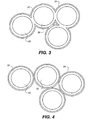
- Figures 3 and 4 illustrate possible core shell arrangements of the particles.
- the core 20 may be a cheap insulating particle such as silica.
- a metal shell 22 encapsulates each core 20.
- the layer of lyophobic material 24 surrounds the shelled particles.
- the layer 24 may be made of, for example, polymer. Other materials which may be used include a polyelectrolyte, a fluoropolymer, a self assembled monolayer (SAM) or an inorganic shell.
- SAM self assembled monolayer
- the invention is not to be taken as limited to these materials.
- the metal cores 20 of the particles 8 in the lower layer 4 should be connected and the lyophobic electrically insulating covering 24 completely encapsulate the structure.
- all particle cores of layer 4 need to be connected to the conductor 14.
- the particles can be individually encapsulated with lyophobic and electrically insulating shells.
- the structure illustrated in Figure 3 will work with both AC and DC operation
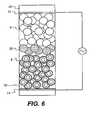
- the liquid 10 has a high advancing contact angle with the particles 8 of the lower layer. Therefore the capillary pressure is such that no liquid 10 will enter the lower layer from the upper layer. The liquid will remain in the upper layer 2 since the lower layer 4 is lyophobic. Thus, with no voltage applied between the conductors 12, 14, and the liquid the liquid 10 resides in the upper layer 2. As the liquid 10 and the particles 6 have a similar refractive index the upper layer will appear essentially transparent or translucent. The particles 8 of the-lower layer 4 - scatter the light. Therefore the colour of the particles in the lower layer can be seen. In the embodiment of the invention including an intermediate layer, see Figure 6, the colour of the particles forming the intermediate layer will be seen.
- Electrowetting is explained in Blake et al, Langmuir 2000, 16, 2928-2935 .
- the voltage applied is in the order of 1 volt, a maximum of 20V being envisaged.
- the applied voltage causes an electrowetting effect which reduces the contact angle of the liquid 10 with the lower layer 4.
- ⁇ is the contact angle in the presence of a voltage
- ⁇ 0 is the contact angle with no voltage
- V is the voltage
- ⁇ is the dielectric constant of the lyophobic layer
- ⁇ 0 is the permittivity of free space
- ⁇ is the liquid surface tension
- d is the thickness of the lyophobic layer.
- ⁇ is the average pore radius within the porous structure. If we define the upper layer as A and the lower layer as B , then liquid moves from the upper to lower layer if ⁇ P A ⁇ ⁇ P B and moves from the lower to upper layer if ⁇ P A ⁇ ⁇ P B
- ⁇ P A is positive and ⁇ P B is negative.
- the capillary pressure is therefore unfavourable for the liquid 10 to move into the lower layer 4.
- ⁇ P B increases until it is greater than ⁇ P A at which point the liquid 10 will move into the lower layer 4.
- the upper layer 2 now largely empty of liquid 10, will strongly scatter light and appear white.
- ⁇ P B will fall and, provided it falls below that of the upper layer 2, the liquid 10 will be drawn back into the upper layer. Note that it is important that the upper layer never completely empties, though the system is self-limiting on application of the voltage such that this cannot easily happen.
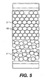
- FIG. 5 A second embodiment of the present invention is illustrated in Figure 5.
- the upper layer 2 is a photonic crystal, for example, opal or inverse opal, structure 18 rather than a random porous structure.
- the photonic crystal structure is very regular and the particle sizes are in the order of the wavelength of light.
- the crystal structure acts as a diffraction grating and reflects only particular wavelengths of light, i.e. particular colours.
- the gaps in the crystal structure are filled with liquid 10
- the photonic nature of the layer 2 is removed and the layer becomes transparent or translucent as described above. Colour from the lower layer 4 is then seen.
- the photonic layer reflects strongly at a wavelength defined by the symmetry and spacing dimension of the crystal structure.
- the upper layer 2 now reflects a colour defined by the size of the photonic crystals. Thus a coloured element could be made.
- a base electrode, lower conductor, was formed by an indium tin oxide (ITO) coating on a poly-ethylene-teraphthalate (PET) base. This was used as supplied and cut into appropriately sized pieces.
- the ITO layer faced upwards and provided a conductive surface onto which the porous display device could be built.
- the ITO base was dip coated (3-4 layers) with a fluoropolymer (Fluoropel 804A, sourced form Cytonix Corporation), which behaved as a hydrophobic dielectric layer.
- the thickness of the layer was approximately 3 ⁇ m.
- the lower porous layer contained 200nm diameter silver particles, which were coated in a layer of octadecyl mercaptan.
- the silver particles were precipitated on the reduction of silver nitrate with sodium borohydride.
- the octadecyl mercaptan was added immediately after precipitation.
- the octadecyl mercaptan gave a hydrophobic and electrically insulating coating to the silver particles.
- the resulting coating showed a step change in capacitance with voltage (at 2V AC peak-peak) when the capacitance was measured with a droplet of 20g/l NaCl solution placed on the surface. This indicated that the drop was being pulled reversibly in and out of the lower porous network.
- An upper porous layer was coated on top of the mercaptan coated silver particles.
- the particles in the upper layer are polystyrene beads which were coated with colloidal silica particles. See US 5455320 and US 5750328 .
- the particles were 650nm diameter.
- the upper layer was coated from an aqueous system prepared with about 25% solids, 0.1% Zonyl FSN and 1.0% gelatin.
- the refractive index of the upper layer of particles was higher than that of water. So in order to increase the refractive index, 80% glycerol solution (20g/l NaCl) was used as the liquid in the device. A switching system was demonstrated. The upper layer of particles was fully wetted with the liquid and any excess liquid removed. At this stage the device had a grey appearance. A needle was then placed onto the upper surface and was in turn connected to the AC power supply. When an AC voltage was applied to the system the area surrounding the tip of the needle turned white. This indicated that the liquid in this area had been drawn down into the lower level and the device had switched. When the applied voltage was removed the area turned back to its original grey colour.
- the elements can be made using coating technology. Initially a substrate comprising a pattern of electrodes is prepared by means such as printing. Subsequently a coating process, either multiple single layer coatings or one or more multi-layer coatings is used to lay down the porous layers.
- the coating process chosen can be unmetered or preferably pre-metered. It is well known in the coating art to manufacture porous particulate layers through single or multi-layer coating processes.
- the layers will then be dried.
- the liquid 10 can then be coated and since the top layer is lyophilic, the liquid will fill the upper layer without penetrating the lower layer.
- a final encapsulating layer is then provided by coating or by lamination and will contain electrodes to connect to the liquid layer.
- a matrix or plurality of elements can be assembled to form a display device.
- the elements of the display device would be environmentally sealed in order to encapsulate the liquid and prevent moisture ingression and liquid loss.
Landscapes
- Chemical & Material Sciences (AREA)
- Engineering & Computer Science (AREA)
- Physics & Mathematics (AREA)
- General Physics & Mathematics (AREA)
- Nanotechnology (AREA)
- Materials Engineering (AREA)
- Condensed Matter Physics & Semiconductors (AREA)
- Crystallography & Structural Chemistry (AREA)
- Composite Materials (AREA)
- Optics & Photonics (AREA)
- Electrochromic Elements, Electrophoresis, Or Variable Reflection Or Absorption Elements (AREA)
- Mechanical Light Control Or Optical Switches (AREA)
- Devices For Indicating Variable Information By Combining Individual Elements (AREA)
Applications Claiming Priority (2)
| Application Number | Priority Date | Filing Date | Title |
|---|---|---|---|
| GB0407643A GB0407643D0 (en) | 2004-04-02 | 2004-04-02 | Display element |
| PCT/GB2005/001063 WO2005096066A1 (en) | 2004-04-02 | 2005-03-22 | Electrowetting display element |
Publications (2)
| Publication Number | Publication Date |
|---|---|
| EP1730575A1 EP1730575A1 (en) | 2006-12-13 |
| EP1730575B1 true EP1730575B1 (en) | 2007-08-15 |
Family
ID=32247847
Family Applications (1)
| Application Number | Title | Priority Date | Filing Date |
|---|---|---|---|
| EP05729449A Expired - Fee Related EP1730575B1 (en) | 2004-04-02 | 2005-03-22 | Electrowetting display element |
Country Status (6)
| Country | Link |
|---|---|
| EP (1) | EP1730575B1 (ja) |
| JP (1) | JP4594378B2 (ja) |
| CN (1) | CN100412606C (ja) |
| DE (1) | DE602005002043T2 (ja) |
| GB (1) | GB0407643D0 (ja) |
| WO (1) | WO2005096066A1 (ja) |
Families Citing this family (10)
| Publication number | Priority date | Publication date | Assignee | Title |
|---|---|---|---|---|
| JP5055750B2 (ja) * | 2005-11-21 | 2012-10-24 | 富士ゼロックス株式会社 | 多色表示材料組成物、光学素子及びその表示方法 |
| JP2008046359A (ja) * | 2006-08-16 | 2008-02-28 | Fuji Xerox Co Ltd | 光学材料、光学素子、光学装置、及び光学素子の表示方法 |
| JP4967541B2 (ja) * | 2006-08-31 | 2012-07-04 | 富士ゼロックス株式会社 | 光学素子及び光学装置 |
| EP2071385B1 (en) * | 2007-12-11 | 2020-07-22 | Miortech Holding B.V. | Electrowetting element |
| US8435397B2 (en) * | 2008-01-25 | 2013-05-07 | Mphase Technologies, Inc. | Device for fluid spreading and transport |
| EP2310144A4 (en) * | 2008-06-16 | 2012-01-04 | Massachusetts Inst Technology | COATINGS |
| EP2425295A4 (en) * | 2009-04-30 | 2013-06-05 | Hewlett Packard Development Co | REFLECTIVE COLOR DISPLAY ARRANGEMENT |
| EP2847627A1 (en) | 2012-04-30 | 2015-03-18 | Université de Namur | Functional multilayer system |
| JP6233596B2 (ja) | 2013-09-09 | 2017-11-22 | パナソニックIpマネジメント株式会社 | 反射型表示素子 |
| US9529188B2 (en) * | 2015-03-25 | 2016-12-27 | Amazon Technologies, Inc. | Electrowetting device with multi layer support plate |
Family Cites Families (13)
| Publication number | Priority date | Publication date | Assignee | Title |
|---|---|---|---|---|
| JPS5569126A (en) * | 1978-11-17 | 1980-05-24 | Matsushita Electric Ind Co Ltd | Light control unit |
| US4419663A (en) * | 1979-03-14 | 1983-12-06 | Matsushita Electric Industrial Co., Ltd. | Display device |
| JPS5789725A (en) * | 1980-11-26 | 1982-06-04 | Matsushita Electric Ind Co Ltd | Display device |
| EP0881071A3 (de) * | 1996-06-12 | 1998-12-09 | Fischer & Krecke Gmbh & Co. | Druckmaschine |
| US5930026A (en) * | 1996-10-25 | 1999-07-27 | Massachusetts Institute Of Technology | Nonemissive displays and piezoelectric power supplies therefor |
| JPH10193784A (ja) * | 1997-01-10 | 1998-07-28 | Fuji Xerox Co Ltd | 可逆的記録媒体 |
| EP0884714A3 (en) * | 1997-06-10 | 1999-09-15 | Xerox Corporation | Electric display sheet |
| US6449081B1 (en) * | 1999-06-16 | 2002-09-10 | Canon Kabushiki Kaisha | Optical element and optical device having it |
| WO2002039462A2 (en) * | 2000-11-09 | 2002-05-16 | Koninklijke Philips Electronics N.V. | Multi-fluid elements device with controllable fluid level by means of matrix addressing |
| JP2004533635A (ja) * | 2001-04-03 | 2004-11-04 | サーノフ コーポレイション | 電磁放射線を制御するために結晶を構成設定し調整する方法及び装置 |
| FR2825481B1 (fr) * | 2001-05-31 | 2003-07-18 | Commissariat Energie Atomique | Structure electrochrome souple et procedes de fabrication de cette structure |
| JP2005115245A (ja) * | 2003-10-10 | 2005-04-28 | Fuji Photo Film Co Ltd | 表示装置 |
| JP4472397B2 (ja) * | 2004-03-25 | 2010-06-02 | シャープ株式会社 | 表示装置 |
-
2004
- 2004-04-02 GB GB0407643A patent/GB0407643D0/en not_active Ceased
-
2005
- 2005-03-22 WO PCT/GB2005/001063 patent/WO2005096066A1/en active IP Right Grant
- 2005-03-22 EP EP05729449A patent/EP1730575B1/en not_active Expired - Fee Related
- 2005-03-22 JP JP2007505613A patent/JP4594378B2/ja not_active Expired - Fee Related
- 2005-03-22 DE DE602005002043T patent/DE602005002043T2/de active Active
- 2005-03-22 CN CNB2005800102358A patent/CN100412606C/zh not_active Expired - Fee Related
Also Published As
| Publication number | Publication date |
|---|---|
| CN100412606C (zh) | 2008-08-20 |
| JP2007531036A (ja) | 2007-11-01 |
| EP1730575A1 (en) | 2006-12-13 |
| DE602005002043D1 (de) | 2007-09-27 |
| WO2005096066A1 (en) | 2005-10-13 |
| JP4594378B2 (ja) | 2010-12-08 |
| CN1938630A (zh) | 2007-03-28 |
| DE602005002043T2 (de) | 2008-05-08 |
| GB0407643D0 (en) | 2004-05-05 |
Similar Documents
| Publication | Publication Date | Title |
|---|---|---|
| EP1730575B1 (en) | Electrowetting display element | |
| EP1730574B1 (en) | Electrowetting display element | |
| Gu et al. | Emerging electrochromic materials and devices for future displays | |
| CN102707536B (zh) | 反射器及具有所述反射器的显示装置 | |
| EP1730573B1 (en) | Electrowetting display element | |
| JP4744757B2 (ja) | アクティブマトリクス駆動電子ディスプレイの性能を高めるための蓄電キャパシタの使用 | |
| US8723759B2 (en) | Display with light concentrating substrate | |
| US6724519B1 (en) | Protective electrodes for electrophoretic displays | |
| US6865010B2 (en) | Electrophoretic electronic displays with low-index films | |
| US6721083B2 (en) | Electrophoretic displays using nanoparticles | |
| US6130774A (en) | Shutter mode microencapsulated electrophoretic display | |
| US20020145792A1 (en) | Electrophoretic displays using nanoparticles | |
| DE112010003038T5 (de) | Anzeigeverfahren und -vorrichtung mit photonischen Kristalleigenschaften | |
| US8432598B2 (en) | Transparent conductor structure | |
| JP2002533754A (ja) | 電気泳動ディスプレイの保護電極 | |
| CN102998791B (zh) | 一种电润湿显示装置 | |
| WO2010126512A1 (en) | Reflective colour display device | |
| DE102015103794B4 (de) | Leuchtvorrichtung mit einer Mikrofluidpumpe zum Verlagern von Fluid und Verfahren zum Betrieb einer solchen Leuchtvorrichtung | |
| CN107065172A (zh) | 一种覆盖可见光至红外波段的宽光谱显示器 | |
| US20130156943A1 (en) | Microcapsule color-patterning method |
Legal Events
| Date | Code | Title | Description |
|---|---|---|---|
| PUAI | Public reference made under article 153(3) epc to a published international application that has entered the european phase |
Free format text: ORIGINAL CODE: 0009012 |
|
| 17P | Request for examination filed |
Effective date: 20060802 |
|
| AK | Designated contracting states |
Kind code of ref document: A1 Designated state(s): DE GB |
|
| GRAP | Despatch of communication of intention to grant a patent |
Free format text: ORIGINAL CODE: EPIDOSNIGR1 |
|
| DAX | Request for extension of the european patent (deleted) | ||
| GRAS | Grant fee paid |
Free format text: ORIGINAL CODE: EPIDOSNIGR3 |
|
| RBV | Designated contracting states (corrected) |
Designated state(s): DE GB |
|
| GRAA | (expected) grant |
Free format text: ORIGINAL CODE: 0009210 |
|
| AK | Designated contracting states |
Kind code of ref document: B1 Designated state(s): DE GB |
|
| REG | Reference to a national code |
Ref country code: GB Ref legal event code: FG4D |
|
| REF | Corresponds to: |
Ref document number: 602005002043 Country of ref document: DE Date of ref document: 20070927 Kind code of ref document: P |
|
| REG | Reference to a national code |
Ref country code: GB Ref legal event code: 711B |
|
| PLBE | No opposition filed within time limit |
Free format text: ORIGINAL CODE: 0009261 |
|
| STAA | Information on the status of an ep patent application or granted ep patent |
Free format text: STATUS: NO OPPOSITION FILED WITHIN TIME LIMIT |
|
| 26N | No opposition filed |
Effective date: 20080516 |
|
| PGFP | Annual fee paid to national office [announced via postgrant information from national office to epo] |
Ref country code: GB Payment date: 20130225 Year of fee payment: 9 |
|
| PGFP | Annual fee paid to national office [announced via postgrant information from national office to epo] |
Ref country code: DE Payment date: 20130328 Year of fee payment: 9 |
|
| REG | Reference to a national code |
Ref country code: DE Ref legal event code: R119 Ref document number: 602005002043 Country of ref document: DE |
|
| GBPC | Gb: european patent ceased through non-payment of renewal fee |
Effective date: 20140322 |
|
| REG | Reference to a national code |
Ref country code: DE Ref legal event code: R119 Ref document number: 602005002043 Country of ref document: DE Effective date: 20141001 |
|
| PG25 | Lapsed in a contracting state [announced via postgrant information from national office to epo] |
Ref country code: DE Free format text: LAPSE BECAUSE OF NON-PAYMENT OF DUE FEES Effective date: 20141001 Ref country code: GB Free format text: LAPSE BECAUSE OF NON-PAYMENT OF DUE FEES Effective date: 20140322 |