EP1729411A1 - Phase circuit, high-frequency switch, and phase device - Google Patents
Phase circuit, high-frequency switch, and phase device Download PDFInfo
- Publication number
- EP1729411A1 EP1729411A1 EP04723718A EP04723718A EP1729411A1 EP 1729411 A1 EP1729411 A1 EP 1729411A1 EP 04723718 A EP04723718 A EP 04723718A EP 04723718 A EP04723718 A EP 04723718A EP 1729411 A1 EP1729411 A1 EP 1729411A1
- Authority
- EP
- European Patent Office
- Prior art keywords
- high frequency
- switching element
- phase shift
- frequency signal
- support film
- Prior art date
- Legal status (The legal status is an assumption and is not a legal conclusion. Google has not performed a legal analysis and makes no representation as to the accuracy of the status listed.)
- Withdrawn
Links
Images








Classifications
-
- H—ELECTRICITY
- H01—ELECTRIC ELEMENTS
- H01P—WAVEGUIDES; RESONATORS, LINES, OR OTHER DEVICES OF THE WAVEGUIDE TYPE
- H01P1/00—Auxiliary devices
- H01P1/10—Auxiliary devices for switching or interrupting
- H01P1/15—Auxiliary devices for switching or interrupting by semiconductor devices
-
- H—ELECTRICITY
- H01—ELECTRIC ELEMENTS
- H01P—WAVEGUIDES; RESONATORS, LINES, OR OTHER DEVICES OF THE WAVEGUIDE TYPE
- H01P1/00—Auxiliary devices
- H01P1/18—Phase-shifters
-
- H—ELECTRICITY
- H03—ELECTRONIC CIRCUITRY
- H03H—IMPEDANCE NETWORKS, e.g. RESONANT CIRCUITS; RESONATORS
- H03H7/00—Multiple-port networks comprising only passive electrical elements as network components
- H03H7/18—Networks for phase shifting
- H03H7/20—Two-port phase shifters providing an adjustable phase shift
Definitions
- the present invention relates to a downsized phase shift circuit having a broadband phase shift amount characteristic, and a high frequency switch and a phase shifter which are used for the phase shift circuit.
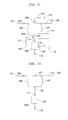
- Fig. 31 is a circuit diagram showing a phase shift circuit disclosed in US 6137377 as a first conventional example.
- a first field effect transistor (hereinafter referred to as "FET") 103 operates as a switch for switching between an on state and an off state, and a first bias terminal 118 is connected to a gate electrode of the first field effect transistor through a first resistor 113.
- the FET 103 When a potential same as that of a drain voltage and a source voltage of the FET 103 is applied to the bias terminal 118, the FET 103 turns on and exhibits a resistivity (hereinafter referred to as "on resistance").
- the FET 103 turns off and exhibits a capacitivity (hereinafter referred to as "off capacitance").
- An FET 104 and an FET 105 operate in the same manner as the FET 103.
- a first resistor 113, a second resistor 114, a third resistor 115, a fourth resistor 116, and a fifth resistor 117 have such a sufficiently large resistance that a high frequency signal inputted from a high frequency signal input terminal 101 cannot pass through the resistors.
- a voltage (disclosed as -5V in US 6137377 ) equal to or lower than the pinch off voltage is constantly applied to a bias terminal 118 and a bias terminal 120.
- a voltage of 0 V or equal to or lower than the pinch off voltage is applied to a bias terminal 119.
- Fig. 32 is an equivalent circuit diagram in which a voltage equal to or lower than the pinch off voltage is applied to the bias terminal 119.
- the FET 103 turns on and exhibits an on resistance 122
- the FET 105 turns off and exhibits an off capacitance 123.
- the circuit shown in Fig. 32 can be regarded as a high pass filter (hereinafter referred to as "HPF") which is composed of a first capacitor 109, a second capacitor 110, a first inductor 106, and a second inductor 107.
- HPF causes a signal inputted from the high frequency signal input terminal 101 to have a phase lead, and the signal is then outputted from a high frequency signal output terminal 102.
- Fig. 33 is an equivalent circuit diagram in which 0 V is applied to the bias terminal 119.
- the FET 103 turns off and exhibits an off capacitance 124
- the FET 104 turns off and exhibits an off capacitance 125
- the FET 105 turns on and exhibits an on resistance 126.
- the circuit shown in Fig. 33 can be regarded as a low pass filter (hereinafter referred to as "LPF") which is composed of the first inductor 106, the second inductor 107, and the off capacitance 125.
- the LPF causes a signal inputted from the high frequency signal input terminal 101 to have a phase delay, and the signal is then outputted from the high frequency signal output terminal 102.
- a difference between the phase lead that is caused by the HPF and the phase delay that is caused by the LPF corresponds to a required phase shift amount.
- the bias terminal 119 When the voltage of 0 V, or equal to or lower than the pinch off voltage is applied to the bias terminal 119, the signal inputted from the high frequency signal input terminal 101 switches over the respective on/off state of the FET 103, the FET 104, and the FET 105 according to the voltage applied to the bias terminal 119, to thereby obtain a desired phase shift amount, and the signal is outputted from the high frequency signal output terminal 102.
- the bias terminal 119 is the only one that gives a control signal for switching each of the states of HPF and LPF.
- Fig. 34 is a circuit diagram showing a phase shift circuit according to a second conventional example disclosed in IEEE IMS2000 Proceedings, "A Compact 5-Bit Phase Shifter MMIC for K-Band Satellite Communication Systems".
- a first FET 127 operates as a switch for switching between the on state and the off state, and when a voltage of a potential same as that of a drain voltage and a source voltage of the first FET 127 is applied to a gate terminal of the first FET 127, the first FET 127 turns on, and exhibits the resistivity (hereinafter referred to as "on resistance"). On the other hand, when a voltage equal to or lower than the pinch off voltage is applied to the gate terminal, the first FET 127 turns off and exhibits the capacitivity (hereinafter referred to as "off capacitance").
- a second FET 128 also operates in the same manner as the first FET 127.
- Fig. 35 is an equivalent circuit diagram when the first FET 127 is turned off and the second FET 128 is turned on.
- a capacity 134 exhibits a synthetic capacity of the off capacitance of the first FET 127 and the capacitor 132, and a resistor 135 exhibits the on resistance of the second FET 128.
- the circuit shown in Fig. 35 can be regarded as a high pass filter (hereinafter referred to as "HPF") which is composed of a synthetic capacity 134, a first inductor 129, and a second inductor 130.
- HPF causes a signal inputted from the high frequency signal input terminal 101 to have a phase lead, and the signal is then outputted from the high frequency signal output terminal 102.
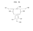
- Fig. 36 is an equivalent circuit diagram when the first FET 127 is turned on and the second FET 128 is turned off.
- a resistor 136 exhibits the on resistance of the first FET 127, and a capacity 137 exhibits the off capacitance of the second FET 128.
- a parallel circuit composed of the third inductor 131 and the off capacitance 137 enters a parallel resonance state at a desired frequency f 0 .
- the circuit shown in Fig. 36 can be regarded as a band pass filter (hereinafter referred to as "BPF") which allows a high frequency signal in the vicinity of the frequency f 0 to pass therethrough when reactances of the first inductor 129 and of the second inductor 130 are sufficiently large.
- BPF band pass filter
- the BPF causes a signal inputted from the high frequency signal input terminal 101 to have a phase changed by substantially 0, and the signal is then outputted from the high frequency signal output terminal 102.
- a difference between the phase lead caused by the HPF and the phase change caused by the BPF corresponds to a required phase shift amount.
- the signal inputted from the high frequency signal input terminal 101 switches between the respective on/off state of the first FET 127 and the second FET 128, to thereby obtain a desired phase shift amount, and is outputted from the high frequency signal output terminal 102.
- phase shift circuit according to the first conventional example shown in Fig. 31 involves such a problem that a large number of circuit structural elements included in the circuit leads to an increased size thereof.
- the phase shift circuit according to the second conventional example shown in Fig. 34 involves such a problem that a phase shift amount that is equal to or higher than 90° is not obtained because the phase circuit has a structure in which the states of the HPF and the BPF are switched.
- the present invention has been made to solve the above problems, and therefore has an object to provide a phase shift circuit which is downsized and has a broadband characteristic, and a high frequency switch and a phase shifter which are used for the phase shift circuit.
- the phase shift circuit is characterized in that the first switching element is constituted by a switching element that is indicative of a through state at a time of on and a capacitivity at a time of off, the second switching element is constituted by a parallel circuit in which an inductor is connected in parallel with a switching element that is indicative of a through state at the time of on and a capacitivity at the time of off, and a series circuit composed of the parallel circuit and the capacitance of the capacitor, and one end of the series circuit is connected to the ground, and the other end of the series circuit is connected to the other ends of the first end second inductors.
- the phase shift circuit is characterized in that the capacitance of the capacitor is constituted by a switching element indicative of the through state at the time of on and the capacitivity at the time of off.
- phase shift circuit is characterized in that the parallel circuit is replaced with a switching element indicative of the through state at the time of on and the capacitivity at the time of off.
- phase shift circuit is characterized in that the switching element indicative of the through state at the time of on and the capacitivity at the time of off is replaced with a parallel circuit that includes a switching element indicative of the through state at the time of on and the capacitivity at the time of off, and a capacitor.
- a high frequency switch includes: a first conductor and a control electrode that are formed on a bottom surface of a cavity embedded in only one surface of a substrate; a dielectric support film that is supported by end portions of the cavity and exists in a hollow through an air layer; a pair of high frequency signal transmission lines formed to be apart from each other at an interval on the support film surface; and a second conductor that is disposed on the rear surface of the support film and forms a parallel plane capacitor between the pair of high frequency signal transmission paths, in which each of the pair of high frequency signal transmission lines has a conductive projection penetrating a part of the support film, and when a voltage is applied to the control electrode, the support film is displaced toward the bottom surface of the cavity, and each of the conductive projections is brought in contact with the first conductor to provide a through state, such that a through/series capacitance switching element that is mechanically driven is structured.
- a high frequency switch includes: a ground conductor and a control electrode which are formed on a bottom surface of a cavity embedded in only one surface of a substrate; a dielectric support film that is supported by end portions of the cavity and exists in a hollow through an air layer; and a high frequency signal transmission line that is formed on the support film surface, in which when a voltage is applied to the control electrode, the support film is displaced toward the bottom surface of the cavity and the support film is brought in contact with the ground conductor to provide a state indicative of the capacitance with respect to the ground, such that a through/series capacitance switching element that is mechanically driven is structured.
- a high frequency switch includes: a pair of high frequency signal transmission lines formed to be apart from each other at an interval on a bottom surface of a cavity that is embedded in only one surface of a substrate and have a conductive projection, respectively; a dielectric film that is formed on the pair of high frequency signal transmission lines to extend across the pair of high frequency signal transmission lines; a first conductor formed on the dielectric film; a dielectric support film supported by end portions of the cavity and exists in a hollow through an air layer; a second conductor formed on a rear surface of the support film; and a control electrode formed on the support film surface, in which when a voltage is applied to the control electrode, the support film is displaced toward the bottom surface of the cavity and the second conductor is brought in contact with the respective conductive projections to provide a through state, such that a through/series capacitance switching element that is mechanically driven is structured.
- a high frequency switch includes: a high frequency signal transmission line that is formed on a bottom surface of a cavity embedded in only one surface of a substrate; a dielectric support film that is supported by end portions of the cavity and exists in a hollow through an air layer; and a ground conductor and a control electrode that are formed on the support film surface, in which when a voltage is applied to the control electrode, the support film is displaced toward the bottom surface of the cavity, and the support film is brought in contact with the high frequency signal transmission line to provide a state indicative of a capacitance with respect to the ground, such that a through/series capacitance switching element that is mechanically driven is structured.
- a phase shift circuit according to the present invention is characterized in that the first switching element is composed of a high frequency switch that constitutes the through/series capacitance switching element, and the second switching element is composed of a high frequency switch that constitutes the through/shunt capacitance switching element.
- phase shifter according to the present invention is characterized in that the above-mentioned phase sift circuits are combined together to constitute a multi-bit phase shifter.
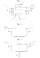
- Fig. 1 is a circuit diagram showing a structure of a phase shift circuit according to a first embodiment of the present invention.
- the phase shift circuit shown in Fig. 1 includes, between a high frequency signal input terminal 1 and a high frequency signal input/output terminal 2, a first switching element 3 for switching between a through path and the capacity of a capacitance C 1 , a second switching element 4 for switching between the through path and the capacity of a capacitance C 2 with respect to a ground, a first inductor 6a, and a second inductor 6b.
- Reference numeral 5 denotes the ground.
- Fig. 2 is an equivalent circuit diagram when a first switching element 3 is in a through state and a second switching element 4 is in a through state.
- the circuit shown in Fig. 2 can be regarded as a through circuit. Accordingly, a signal that is inputted from the high frequency signal input terminal 1 is outputted from the high frequency signal output terminal 2 without producing a phase change. In this situation, there is no reflection loss because the through circuit is matched in all of the frequencies.
- Fig. 3 is an equivalent circuit diagram when the first switching element 3 is in a state indicative of the capacitivity, and the second switching element 4 is in a state indicative of the capacitivity with respect to the ground.
- the circuit shown in Fig. 3 can be regarded as an all pass network that is composed of the first inductor 6a, the second inductor 6b, a first capacitor 7, and a second capacitor 8, the first capacitor 3 exhibiting a capacitivity to form the first capacitor 7, the second switching element 4 also exhibiting a capacitivity to form the second capacitor 8.
- the signal that is inputted from the high frequency signal input terminal 1 is outputted from the high frequency signal output terminal 2 with a phase delay caused by the all pass network.
- the phase shift circuit according to the first embodiment shown in Fig. 1 switches between the through state and the all pass network state due to the switching operation of the first switching element 3 and the switching operation of the second switching element 4, and changes a pass phase that occurs when the signal which is inputted from the high frequency signal input terminal 1 is outputted to the high frequency signal output terminal 2.
- the inductance L, the capacitance C1, and the capacitance C2 are appropriately set, thereby making it possible to obtain a desired phase shift amount over a broadband.
- the phase shift circuit that operates over the broader band than the conventional example.
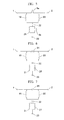
- Fig. 4 is a circuit diagram showing a structure of a phase shift circuit according to a second embodiment of the present invention.
- the phase shift circuit shown in Fig. 4 is structured on a semiconductor substrate 18 in a monolithic fashion, and correspondences of the respective structural elements shown in Fig. 4 to the respective structural elements shown in Fig. 1 are stated below.
- a first FET 8a corresponds to the first switch element 3
- a second FET 8b corresponds to the second switching element 4
- a first spiral inductor 9 corresponds to the first inductor 6a
- a second spiral inductor 10 corresponds to the second inductor 6b, respectively.
- a control electrode of the first FET 8a is connected with a first control signal terminal 16 through a first resistor 13, and a control electrode of the second FET 8b is connected with a second control signal terminal 17 through a second resistor 14.
- the second FET 8b is connected in parallel with a third spiral inductor 11 to constitute a parallel circuit, and the parallel circuit is connected in series to an MIM capacitor 12 to constitute a series circuit.
- One end of the series circuit is connected to the ground through a through hole 15, and the other end of the series circuit is connected to a node between the first and second spiral inductors 9 and 10.
- Fig. 5 is an equivalent circuit diagram showing a phase shift circuit according to the second embodiment shown in Fig. 4.
- An inductor 19 corresponds to the spiral inductor 9
- an inductor 20 corresponds to the second spiral inductor 10
- an inductor 21 corresponds to the third spiral inductor 11
- a capacitor 22 corresponds to the MIM capacitor 12
- a ground 23 corresponds to the through hole 15, respectively.
- the FET 8a and the FET 8b function as switches for switching over the on/off states.
- the FET 8a when a voltage of the same potential as the drain voltage and the source voltage is applied to the gate terminal, the FET 8a becomes in an on state and exhibits the resistivity (hereinafter referred to as "on resistance").
- the FET 8a when a voltage that is equal to or lower than the pinch off voltage is applied to the gate terminal, the FET 8a becomes in an off state and exhibits the capacitivity (hereinafter referred to as "off capacitance").
- the FET 8b also conducts the same operation.
- Fig. 6 is an equivalent circuit diagram when the FET 8a is in an on state and the FET 8b is in an off state in Fig. 5. As shown in Fig. 6, the FET 8a is expressed as an on resistance 24 in an on state, and the FET 8b is expressed as an off capacitance 25 in an off state.
- a parallel circuit composed of the inductor 21 and the off capacitance 25 is set in a parallel resonance (open) state at a desired frequency f 0 .
- the circuit shown in Fig. 6 can be regarded as a band pass filter circuit that has frequencies in the vicinity of the desired frequency f 0 as a pass band.
- the on resistance 24 is sufficiently small, the phase change hardly occurs. Therefore, at the desired frequency f 0 , the signal that is inputted from the high frequency signal input terminal 1 is outputted from the high frequency signal output terminal 2 with no phase change.
- Fig. 7 is an equivalent circuit diagram when the FET 8a is in an off state and the FET 8b is in an on state in Fig. 5. As shown in Fig. 7, the FET 8a is expressed as an off capacitance 26 in an off state, and the FET 8b is expressed as an on resistance 27 in an on state.
- a parallel circuit composed of the on resistance 27 and the inductor 21 can be regarded as a circuit composed of only the on resistance 27. Accordingly, the circuit shown in Fig. 7 can be regarded as an all pass network that is composed of the inductor 19, the inductor 20, the off capacitance 26, and the capacitor 22. Therefore, the signal that is inputted from the high frequency signal input terminal 1 is outputted from the high frequency signal output terminal 2 with a phase delay which is caused by the all pass network.
- phase shift circuit according to the second embodiment shown in Fig. 4 switches between the band pass filter circuit and the all pass network due to the on/off switching operation of the FET 8a and the FET 8b to change the pass phase from the high frequency signal input terminal 1 to the high frequency signal output terminal 2.
- phase shift circuit in the phase shift circuit according to the second embodiment of the present invention, a desired phase shift amount can be obtained by a change in the pass phase.
- the circuit can be structured by two FETs, three inductors, one capacitor, and one through hole, the circuit is downsized as compared with the first conventional example.
- the cutoff frequency of the high pass filter is set to be lower than a desired center frequency.
- the cutoff frequency (a frequency at which the characteristic of the low pass filter and the characteristic of the high pass filter switch from one to another) of the all pass network is higher than the desired center frequency, the inductance and the capacitance can be reduced as compared with those in the second conventional example, to thereby make it possible to downsize the circuit.
- the phase shift circuit is broadened in the band as compared with the first and second conventional examples.
- a change in pass phase which is obtained by the low pass filter and the high pass filter is 90° at the maximum.
- the all pass network is matched in all of the frequencies by appropriately setting the circuit constant, an arbitrary pass phase change, that is, an arbitrary phase shift amount can be obtained.
- the FET 8a and the FET 8b are used as the switching elements.
- an element of any type can be applied as long as the element has a switching function that is capable of switching over the on/off states.
- phase shift circuit according to the second embodiment shown in Fig. 4 is structured on the semiconductor substrate 18 in a monolithic fashion.
- a passive element is formed on a dielectric substrate
- an active element is formed on a semiconductor substrate, and both of those substrates are electrically connected to each other by a metal wire, a metal bump, or the like to constitute a phase shift circuit.
- Fig. 8 is a circuit diagram showing a structure of a phase shift circuit according to a third embodiment of the present invention.
- the same parts as or the corresponding parts to those shown in Fig. 5 are denoted by identical reference symbols, and their duplex descriptions wiii be omitted.
- the capacitor 22 in the phase shift circuit according to the second embodiment shown in Fig. 5 is replaced with an FET 28.
- the FET 28 functions as a switch for switching the on/off state, and conducts the same operation as the FET 8a and the FET 8b.
- Fig. 9 is an equivalent circuit diagram when the FET 8a is in an on state, the FET 8b is in an off state, and the FET 28 is in an on state in Fig. 8.
- the FET 8a is expressed as an on resistance 24 in an on state
- the FET 8b is expressed as an off capacitance 25 in an off state
- the FET 28 is expressed as an on resistance 29 in an on state.
- a parallel circuit composed of the inductor 21 and the off capacitance 25 is set in a parallel resonance (open) state at a desired frequency f 0 . Since a reactance caused by the inductor 19 and the inductor 20 is sufficiently large, the circuit shown in Fig. 9 can be regarded as a band pass filter circuit that has frequencies in the vicinity of the desired frequency f 0 as a pass band. When the on resistance 24 is sufficiently small, the phase change hardly occurs. Therefore, at the desired frequency f0, the signal that is inputted from the high frequency signal input terminal 1 is outputted from the high frequency signal output terminal 2 with no phase change.
- the equivalent circuit shown in Fig. 6 has a series circuit that is mainly composed of the inductor 19, the inductor 21, and the capacitor 22, which may be in a series resonance state at a frequency lower than the desired frequency f 0 , and may affect the characteristic of the phase shift circuit in the vicinity of f 0 .
- the circuit shown in Fig. 9 has the capacitor 22 replaced with the on resistance 29 so as to prevent series resonance, thereby not affecting the characteristic of the phase shift circuit in the vicinity of f 0 with an excellent characteristic.
- Fig. 10 is an equivalent circuit diagram when the FET 8a is in an off state, the FET 8b is in an on state, and the FET 28 is in an off state in Fig. 8.
- the FET 8a is expressed as an off capacitance 26 in an off state
- the FET 8b is expressed as an on resistance 27 in an on state
- the FET 28 is expressed as an off capacitance 30 in an off state.
- a parallel circuit composed of the on resistance 27 and the inductor 21 can be regarded as a circuit composed of only the on resistance 27.
- the circuit shown in Fig. 10 can be regarded as an all pass network that is composed of the inductor 19, the inductor 20, the off capacitance 26, and the off capacitance 30. Therefore, the signal that is inputted from the high frequency signal input terminal 1 is outputted from the high frequency signal output terminal 2 with a phase delay which is caused by the all pass network.
- the capacitance of the off capacitance 26 is C 1
- the capacitance of the off capacitance 30 is C 2
- the inductance of the inductor 19 and the inductor 20 is L
- the characteristic impedance of the high frequency signal input terminal 1 and the high frequency signal output terminal 2 are Z 0 .
- the capacitance C 1 (or C 2 ) is appropriately set, thereby making it possible to obtain a desired phase delay at a desired frequency.
- the phase shift circuit according to the third embodiment shown in Fig. 8 switches between the band pass filter circuit and the all pass network due to the on/off switching operation of the FET 8a, the FET 8b, and the FET 28 to change the pass phase from the high frequency signal input terminal 1 to the high frequency signal output terminal 2.
- phase shift circuit according to the third embodiment the same effects as those in the phase shift circuit according to the second embodiment can be obtained. Also, because the series resonance at the frequency that is equal to or lower than the desired frequency f 0 does not occur in the state of the band pass filter circuit, there is an advantage in that the phase shift circuit does not affect the characteristic of the phase shift circuit in the vicinity of f 0 .
- the FET 8a, FET 8b, and the FET 28 are used as the switching elements.
- an element of any type can be applied as long as the element has a switching function that is capable of switching over the on/off states.
- phase shift circuit according to the third embodiment shown in Fig. 8 may be structured on the semiconductor substrate in a monolithic fashion.
- a passive element is formed on a dielectric substrate
- an active element is formed on a semiconductor substrate, and both of those substrates are electrically connected to each other by a metal wire, a metal bump, or the like to constitute a phase shift circuit.
- Fig. 11 is a circuit diagram showing a structure of a phase shift circuit according to a fourth embodiment of the present invention.
- the same parts as or the corresponding parts to those shown in Fig. 5 are denoted by identical reference symbols, and their duplex descriptions will be omitted.
- the parallel circuit composed of an inductor 21 and an FET 8b in the phase shift circuit according to the second embodiment shown in Fig. 5 is replaced only with the FET 8b.
- Fig. 12 is an equivalent circuit diagram when the FET 8a is in an on state and the FET 8b is in an off state in Fig. 11. As shown in Fig. 12, the FET 8a is expressed as an on resistance 24 in an on state, and the FET 8b is expressed as an off capacitance 25 in an off state.
- the synthetic capacity of the capacitor 22 and the off capacitance 25 is set in a substantially open state.
- the circuit shown in Fig. 12 can be regarded as a through circuit caused by the on resistance 24 since the reactance of the inductor 19 and the inductor 20 is sufficiently large. When the on resistance 24 is sufficiently small, the phase change hardly occurs. Therefore, the signal that is inputted from the high frequency signal input terminal 1 is outputted from the high frequency signal output terminal 2 with no phase change.
- Fig. 13 is an equivalent circuit diagram when the FET 8a is in an off state and the FET 8b is in an on state in Fig. 11.
- the FET 8a is expressed as an off capacitance 26 in an off state
- the FET 8b is expressed as an on resistance 27 in an on state.
- the circuit shown in Fig. 13 can be regarded as an all pass network that is composed of the inductor 19, the inductor 20, the capacitor 22, and the off capacitance 26. Therefore, the signal that is inputted from the high frequency signal input terminal 1 is outputted from the high frequency signal output terminal 2 with a phase delay which is caused by the all pass network.
- phase shift circuit according to the fourth embodiment shown in Fig. 11 switches between the band pass filter circuit and the all pass network due to the on/off switching operation of the FET 8a and the FET 8b to change the pass phase from the high frequency signal input terminal 1 to the high frequency signal output terminal 2.
- phase shift circuit of the fourth embodiment the same effects as those in the phase shift circuit according to the second embodiment can be obtained, and the number of inductors can be reduced by one as compared with the phase shift circuit according to the second embodiment, to thereby make it possible to downsize the phase shift circuit.
- the FET 8a and the FET 8b are used as the switching elements.
- an element of any type can be applied as long as the element has a switching function that is capable of switching over the on/off states.
- phase shift circuit according to the fourth embodiment shown in Fig. 11 may be structured on the semiconductor substrate in a monolithic fashion.
- a passive element is formed on a dielectric substrate
- an active element is formed on a semiconductor substrate, and both of those substrates are electrically connected to each other by a metal wire, a metal bump, or the like to constitute a phase shift circuit.
- Fig. 14 is a circuit diagram showing a structure of a phase shift circuit according to a fifth embodiment of the present invention.
- the same parts as or the corresponding parts to those shown in Fig. 5 are denoted by identical reference symbols, and their duplex descriptions will be omitted.
- the FET 8a of the phase shift circuit according to the second embodiment shown in Fig. 5 is connected in parallel with the capacitor 31, and the FET 8b is connected in parallel with the capacitor 32.
- the same operation as that in Fig. 6 is conducted when the FET 8a is in an on state and the FET 8b is in an off state.
- the off capacitance of the FET 8b can be reduced by adding the capacitor 32 as compared with the case of one FET 8b. In other words, the size of the FET 8b can be reduced.
- the same operation as that in Fig. 7 is conducted when the FET 8a is in an off state and the FET 8b is in an on state.
- the off capacitance of the FET 8a can be reduced by adding the capacitor 31 as compared with the case of one FET 8a. In other words, the size of the FET 8a can be reduced.
- phase shift circuit according to the fifth embodiment shown in Fig. 14 the same effects as those in the second embodiment can be obtained, and the size of the FET can be reduced as compared with the phase shift circuit according to the second embodiment, to thereby make it possible to realize the phase shift circuit.
- the FET 8a and the FET 8b are used as the switching elements.
- an element of any type can be applied as long as the element has a switching function that is capable of switching over the on/off states.
- phase shift circuit according to the fifth embodiment shown in Fig. 14 may be structured on the semiconductor substrate in a monolithic fashion.
- a passive element is formed on a dielectric substrate
- an active element is formed on a semiconductor substrate, and both of those substrates are electrically connected to each other by a metal wire, a metal bump, or the like to constitute a phase shift circuit.
- Fig. 15 is a top view showing the structure of a phase shift circuit that is formed on a substrate according to a sixth embodiment of the present invention.
- Fig. 15 shows the structure in the case of a coplanar line structure.
- a first dielectric support film 40 is supported by an end portion of a first cavity 39 that is embedded from one surface of the substrate 35 through a fine machining technique, and exists in a hollow through an air layer.
- Formed on the dielectric support film 40 are a first meander line 38a and a second meander line 38b.
- An interval between a bottom surface of the cavity 39 and the dielectric support film 40 is several microns to several tens microns.
- the bottom surface of the cavity 39 may be covered with a metal or not.
- Reference numeral 33 and 34 denotes a high frequency signal input terminal and a high frequency signal output terminal
- reference numeral 36 and 37 denotes a through/series capacitance switching element and a through/shunt capacitance switching element which are formed on the substrate 35.
- Fig. 16 is an exploded diagram showing the detailed structure of the through/series capacitance switching element 36 shown in Fig. 15. As shown in Fig. 16, a control electrode 43 and a contact metal 44 are formed on a bottom surface of a second cavity 42 which is embedded from one surface of a substrate 41 (the same as the substrate 35 shown in Fig. 15) through a fine machining technique.
- Through holes 46a and 46b are defined in a second dielectric support film 45 that is supported at right and left end portions of the second cavity 42 and exists in the hollow through an air layer, and a metal 47 is formed on a lower surface (back surface) of the second dielectric support film 45.
- First and second high frequency signal transmission lines 48a and 48b are located on the surface of the second dielectric support film 45 at a distance, and first and second ground metals 49a and 49b are disposed on the surface of the second dielectric support film 45.
- the first high frequency signal transmission line 48a, the second high frequency signal transmission line 48b, the first ground metal 49a, and the second ground metal 49b form a coplanar line having a gap in the center thereof.
- the coplanar line is formed on an upper surface of the second dielectric support film 45.
- the first high frequency signal transmission line 48a has a metal pattern passing through the second dielectric support film 45 in the through hole 46a portion.
- the second high frequency signal transmission line 48b has a metal pattern passing through the second dielectric support film 45 in the through hole 46b portion.
- the second dielectric support film 45 having the coplanar line exists in a hollow through the air layer of the second cavity 42, and an interval between the bottom surface of the second cavity 42 and the second dielectric support film 45 is several microns to several tens microns.
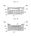
- Fig. 17 is a cross-sectional view showing a through/series capacitance switching element 36 taken along the line A-A' shown in Fig. 15 when no voltage is applied to a control electrode 43.
- the metal 47, the first high frequency signal transmission line 48a, and the second dielectric support film 45 form a capacitance. Also, the metal 47, the second signal line 48b, and the second dielectric support film 45 also form a capacitance. In other words, a series capacitance state is obtained.
- Fig. 18 is a cross-sectional view showing a through/series capacitance switching element 36 taken along the line A-A' shown in Fig. 15 when a voltage is applied to a first control electrode 43.
- An electrostatic attraction force is exerted between a first ground metal 49a and the first control electrode 43 and between a second ground metal 49b and the first control electrode 43 so that the second dielectric support film 45 is displaced toward the bottom surface of the second cavity 42.
- the first high signal transmission line 48a and the second high signal transmission line 48b are rendered conductive through the contact metal 44 to obtain the through state.
- Fig. 19 is an exploded diagram showing the detailed structure of a through/shunt capacitance switching element 37 shown in Fig. 15.
- a second control electrode 51 and a ground metal 52 are formed on a bottom surface of a third cavity 50 which is embedded from one surface of the substrate 41 through a fine machining technique and on the substrate 41.
- a third dielectric support film 53 is supported at the right and left end portions of the cavity 50 and exists in a hollow through an air layer.
- a third high frequency signal transmission line 54, a third ground metal 55a, and a fourth ground metal 55b are formed on an upper surface of the dielectric support film 53.
- the third high frequency signal transmission line 54, the ground metal 52, the third ground metal 55a, and the fourth ground metal 55b constitute a grounded coplanar line.
- An interval of several microns to several tens microns are defined between the bottom surface of the third cavity 50 and the third dielectric support film 53.
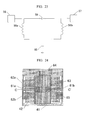
- Fig. 20 is a cross-sectional view showing the through/shunt capacitance switching element 37 taken along the line B-B' shown in Fig. 15 when a voltage is not applied to a second control electrode 51.
- the high frequency signal is transmitted through the grounded coplanar. In other words, the through state is obtained.
- Fig. 21 is a cross-sectional view showing a through/shunt capacitance switching element 37 taken along the line B-B' shown in Fig. 15 when a voltage is applied to the second control electrode 51.
- An electrostatic attraction force is exerted between a third ground metal 55a and the second control electrode 51 and between a fourth ground metal 55b and the second control electrode 51 so that the third dielectric support film 53 is displaced toward the bottom surface of the third cavity 50.
- the third high frequency signal transmission line 54 and the ground metal 52 are brought in contact with each other through the third dielectric support film 53. In other words, a state indicative of the capacitance with respect to the ground is obtained.
- Fig. 22 is an equivalent circuit diagram when the through/series capacitance switching element 36 is in a through state, and the through/shunt capacitance switching element 37 is in a through state, in the phase shift circuit shown in Fig. 15.
- a voltage is applied to the first control electrode 43, and no voltage is applied to the second control electrode 51 (the same potential as the ground).
- Reference symbol 56 denotes a terminal corresponding to the high frequency signal input terminal 33
- 57 is a terminal corresponding to the high frequency signal output terminal 34
- 58a is an inductor corresponding to the first meander line 38a
- 58b is an inductor corresponding to the second meander line 38b.
- the circuit shown in Fig. 22 can be regarded as a through circuit. Accordingly, a signal that is inputted from the high frequency signal input terminal 56 is outputted from the high frequency signal output terminal 57 without producing a phase change. In this situation, there is no reflection loss because the through circuit is matched in all of the frequencies.
- Fig. 23 is an equivalent circuit diagram when the through/series capacitance switching element 36 is in a series capacitance state, and the through/shunt capacitance switching element 37 is in a shunt capacitance state, in the phase shift circuit shown in Fig. 15. In this situation, no voltage is applied to the first control electrode 43 (the same potential as the ground), and a voltage is applied to the second control electrode 51.
- the same parts as or the corresponding parts to those shown in Fig. 22 are denoted by identical reference symbols, and their duplex descriptions will be omitted.
- a capacitor 59 is exhibited when the through/series capacitance switching element 36 is in the series capacitance state, and a capacitor 60 is a capacitor with respect to the ground which is exhibited when the through/shunt capacitance switching element 37 is in the shunt capacitance state.
- the circuit shown in Fig. 23 can be regarded as an all pass network that is composed of the inductor 58a, the inductor 58b, the capacitor 59, and the capacitor 60.
- the signal that is inputted from the high frequency signal input terminal 56 is outputted from the high frequency signal output terminal 57 with a phase delay caused by the all pass network.
- the phase shift circuit according to the sixth embodiment shown in Fig. 15 switches between the through state and the all pass network state due to the switching operation of the through/series capacitance switching element 36 and the switching operation of the through/shunt capacitance switching element 37, and changes the pass phase occurring when the signal that is inputted from the high frequency signal input terminal 56 is outputted to the high frequency signal output terminal 57.
- the inductance L, the capacitance C1, and the capacitance C2 are appropriately set, thereby making it possible to obtain a desired phase shift amount over a broadband.
- the phase shift circuit that operates over the broader band than the conventional example.
- phase shift circuit according to the sixth embodiment shown in Fig. 15 obtains the same effects as those in the first to fifth embodiments.
- the lower loss is obtained as compared with a case of using the switching element of a semiconductor as in the second to fifth embodiments by using the fine machining technique because the through/series capacitance switching element and the through/shunt capacitance switching element which are mechanically driven are used for the switching element.
- the hollow structure is applied by using the fine machining technique, the high frequency characteristic is hardly affected by the substrate.
- an inexpensive substrate such as a low resistance silicon substrate or a glass substrate can be used, which can reduce the costs as compared with a case of using a semiconductor substrate.
- a hollow structure meander line of a cavity which is formed by fining one side of the substrate is applied as the inductor.
- a spiral inductor that is formed by patterning both surfaces of the dielectric support film may be applied.
- the meander line may be formed on the substrate.
- the high frequency signal transmission line is formed on the dielectric support film.
- a dielectric support film is further formed on the high frequency signal transmission line to constitute a three layer structure.
- Fig. 24 is a top view showing the details of a through/series capacitance switching element in a phase shift circuit according to a seventh embodiment of the present invention.
- the same parts as or the corresponding parts to those shown in Fig. 16 are denoted by identical reference symbols, and their duplex descriptions will be omitted.
- a fifth high frequency signal transmission line 61 a, a sixth high frequency signal transmission line 61 b, a fifth ground metal 62a, and a sixth ground metal 62b are formed on the bottom surface of the cavity 42 that is embedded in only one surface of the substrate 41 to constitute a coplanar line having a gap in the center thereof.
- a fourth dielectric support film 63 is supported by ends of the cavity 42 and exists in a hollow through an air layer of the cavity 42.
- a third control electrode 64 is formed on the fourth dielectric support film 63, and a contact metal 65 is formed on a rear surface of the fourth dielectric support film 63.
- An interval of several microns to several tens microns are formed between the bottom surface of the cavity 42 and the fourth dielectric support film 63.
- Fig. 25 is a cross-sectional view taken along the line C-C' shown in Fig. 24 when no voltage is applied to the third control electrode 64.
- a metal 67 is formed on a dielectric film 66, and the metal 67, the fifth high frequency signal transmission line 61 a, and the dielectric film 66 form a capacitance.
- the metal 67, the sixth high frequency signal transmission line 61 b, and the dielectric film 66 form a capacitance. In other words, a series capacitance state is obtained.
- Fig. 26 is a cross-sectional view taken along the line C-C' shown in Fig. 24 when a voltage is applied to the third control electrode 64.
- an electrostatic attraction force is exerted between the fifth ground metal 62a and the third control electrode 64 and between the sixth ground metal 62b and the third control electrode 64 so that the fourth dielectric support film 63 is displaced toward the bottom surface of the cavity 42.
- the fifth signal transmission line 61 a and the sixth signal transmission line 61 b are rendered conductive through the contact metal 65 to obtain the through state.
- Fig. 27 is a top view showing the details of a through/shunt capacitance switching element in a phase shift circuit according to the seventh embodiment of the present invention.
- a seventh high frequency signal transmission line 68, a seventh ground metal 69a, and an eighth ground metal 69b are formed on the bottom surface of the cavity 42 that is embedded in only one surface of the substrate 41, to thereby constitute a coplanar line.
- a fifth dielectric support film 70 is supported by the ends of the cavity 42 and exists in a hollow through the air layer.
- a metal 71 and a fourth control electrode 72 are formed on the fifth dielectric support film 70.
- An interval between the bottom surface of the cavity 42 and the dielectric support film 70 is several microns to several tens microns.
- the metal 71, the seventh ground metal 69a, and the eighth ground metal 69b are connected to each other on the substrate 41, and the metal 71 has the same potential as the ground.
- Fig. 28 is a cross-sectional view taken along the line D-D' when no voltage is applied to a fourth control electrode 72 shown in Fig. 27.
- the high frequency signal is transmitted through the coplanar line on the bottom surface of the cavity 42. In other words, the through state is obtained.
- Fig. 29 is a cross-sectional view taken along the line D-D' when a voltage is applied to the fourth control electrode 72 shown in Fig. 27.
- An electrostatic attraction force is exerted between the seventh ground metal 69a and the fourth control electrode 72 and between the eighth ground metal 69b and the fourth control electrode 72 so that the fourth dielectric support film 70 is displaced toward the bottom surface of the cavity 42.
- the seventh signal transmission line 68 and the metal 71 are brought in contact with each other through the fifth dielectric support film 70. In other words, a state indicative of the capacitance with respect to the ground is obtained.
- the through/series capacitance switching element 36 is replaced with the through/series capacitance switching element shown in Fig. 24, and the through/shunt capacitance switching element 37 is replaced with the through/shunt capacitance switching element shown in Fig. 27.
- the operation is identical with that in the phase shift circuit according to the sixth embodiment.
- the phase shift circuit according to the seventh embodiment obtains the same effects as those in the first to sixth embodiments.
- the lower loss is obtained as compared with a case of using the switching element of a semiconductor as in the second to fifth embodiments by using the fine machining technique because the through/series capacitance switching element and the through/shunt capacitance switching element which are mechanically driven are used for the switching element.
- the hollow structure is applied by using the fine machining technique, the high frequency characteristic is hardly affected by the substrate.
- an inexpensive substrate such as a low resistance silicon substrate or a glass substrate can be used, which can reduce the costs as compared with a case of using a semiconductor substrate.
- a hollow structure meander line of a cavity which is formed by fining one side of the substrate is applied as the inductor.
- a spiral inductor that is formed by patterning both surfaces of the dielectric support film may be applied.
- the meander line may be formed on the substrate.
- a metal pattern is formed on the dielectric support film.
- a dielectric support film is further formed on the metal pattern to constitute a three layer structure.
- FIG. 30 is a block diagram showing a structure of a phase shifter according to an eighth embodiment of the present invention.
- a plurality of phase shift circuits 75 (75a, 75b, 75c) for one bit are connected in a multistage manner between a high frequency signal input terminal 73 and a high frequency signal output terminal 74.
- the phase shift circuits 75 use the phase shift circuits of the first to seventh embodiments.
- the phase shift circuits 75 for one bit are connected in the multistage manner to constitute the phase shifter, thereby making it possible to realize a phase shifter that operates with multi-bits.
- phase shift circuit which is downsized and has a broadband phase shift amount characteristic
- a high frequency switch that is used for the phase shift circuit.
- multi-bit phase shifter which is downsized and has a broadband phase shift amount characteristic.
Landscapes
- Networks Using Active Elements (AREA)
- Electronic Switches (AREA)
Abstract
Provided is a small-size phase shift circuit having a broad band characteristic. The phase shift circuit includes: a first switching element for switching between a through path and a capacitance capacity; a second switching element for switching the capacitance capacity for the through path and the ground; and a first and a second inductor having inductance. One end of the first switching element is connected to one end of the second switching element by the first inductor while the other ends of the first and the second switching element are connected to each other by the second inductor. One end of the first switching element is connected to a high-frequency signal input terminal while the other end of the first switching element is connected to a high-frequency signal output terminal. Thus, it is possible to constitute a phase device satisfying a predetermined condition.
Description
- The present invention relates to a downsized phase shift circuit having a broadband phase shift amount characteristic, and a high frequency switch and a phase shifter which are used for the phase shift circuit.
- Fig. 31 is a circuit diagram showing a phase shift circuit disclosed in
US 6137377 as a first conventional example. - In the phase shift circuit shown in Fig. 31, a first field effect transistor (hereinafter referred to as "FET") 103 operates as a switch for switching between an on state and an off state, and a
first bias terminal 118 is connected to a gate electrode of the first field effect transistor through afirst resistor 113. - When a potential same as that of a drain voltage and a source voltage of the
FET 103 is applied to thebias terminal 118, theFET 103 turns on and exhibits a resistivity (hereinafter referred to as "on resistance"). - On the other hands, when a gate voltage equal to or lower than a pinch off voltage is applied to the
bias terminal 118, theFET 103 turns off and exhibits a capacitivity (hereinafter referred to as "off capacitance"). An FET 104 and an FET 105 operate in the same manner as the FET 103. - A
first resistor 113, asecond resistor 114, athird resistor 115, afourth resistor 116, and afifth resistor 117 have such a sufficiently large resistance that a high frequency signal inputted from a high frequencysignal input terminal 101 cannot pass through the resistors. - A voltage (disclosed as -5V in
US 6137377 ) equal to or lower than the pinch off voltage is constantly applied to abias terminal 118 and abias terminal 120. A voltage of 0 V or equal to or lower than the pinch off voltage is applied to abias terminal 119. - Subsequently, a description will be given of an operation of the phase shift circuit shown in Fig. 31.
- Fig. 32 is an equivalent circuit diagram in which a voltage equal to or lower than the pinch off voltage is applied to the
bias terminal 119. In this situation, the FET 103 turns on and exhibits an onresistance 122, and the FET 105 turns off and exhibits an offcapacitance 123. - The circuit shown in Fig. 32 can be regarded as a high pass filter (hereinafter referred to as "HPF") which is composed of a
first capacitor 109, asecond capacitor 110, afirst inductor 106, and asecond inductor 107. The HPF causes a signal inputted from the high frequencysignal input terminal 101 to have a phase lead, and the signal is then outputted from a high frequencysignal output terminal 102. - Also, Fig. 33 is an equivalent circuit diagram in which 0 V is applied to the
bias terminal 119. In this situation, the FET 103 turns off and exhibits an offcapacitance 124, the FET 104 turns off and exhibits an offcapacitance 125, and the FET 105 turns on and exhibits an onresistance 126. - The circuit shown in Fig. 33 can be regarded as a low pass filter (hereinafter referred to as "LPF") which is composed of the
first inductor 106, thesecond inductor 107, and the offcapacitance 125. The LPF causes a signal inputted from the high frequencysignal input terminal 101 to have a phase delay, and the signal is then outputted from the high frequencysignal output terminal 102. - A difference between the phase lead that is caused by the HPF and the phase delay that is caused by the LPF corresponds to a required phase shift amount. When the voltage of 0 V, or equal to or lower than the pinch off voltage is applied to the
bias terminal 119, the signal inputted from the high frequencysignal input terminal 101 switches over the respective on/off state of theFET 103, theFET 104, and theFET 105 according to the voltage applied to thebias terminal 119, to thereby obtain a desired phase shift amount, and the signal is outputted from the high frequencysignal output terminal 102. In other words, of the bias terminals, thebias terminal 119 is the only one that gives a control signal for switching each of the states of HPF and LPF. - Then, Fig. 34 is a circuit diagram showing a phase shift circuit according to a second conventional example disclosed in IEEE IMS2000 Proceedings, "A Compact 5-Bit Phase Shifter MMIC for K-Band Satellite Communication Systems".
- In the phase shift circuit shown in Fig. 34, a
first FET 127 operates as a switch for switching between the on state and the off state, and when a voltage of a potential same as that of a drain voltage and a source voltage of thefirst FET 127 is applied to a gate terminal of thefirst FET 127, thefirst FET 127 turns on, and exhibits the resistivity (hereinafter referred to as "on resistance"). On the other hand, when a voltage equal to or lower than the pinch off voltage is applied to the gate terminal, thefirst FET 127 turns off and exhibits the capacitivity (hereinafter referred to as "off capacitance"). A second FET 128 also operates in the same manner as the first FET 127. - Subsequently, a description will be given of an operation of the phase shift circuit shown in Fig. 34.
- Fig. 35 is an equivalent circuit diagram when the
first FET 127 is turned off and thesecond FET 128 is turned on. Acapacity 134 exhibits a synthetic capacity of the off capacitance of thefirst FET 127 and thecapacitor 132, and aresistor 135 exhibits the on resistance of thesecond FET 128. In this situation, the circuit shown in Fig. 35 can be regarded as a high pass filter (hereinafter referred to as "HPF") which is composed of asynthetic capacity 134, afirst inductor 129, and asecond inductor 130. The HPF causes a signal inputted from the high frequencysignal input terminal 101 to have a phase lead, and the signal is then outputted from the high frequencysignal output terminal 102. - Also, Fig. 36 is an equivalent circuit diagram when the
first FET 127 is turned on and thesecond FET 128 is turned off. Aresistor 136 exhibits the on resistance of thefirst FET 127, and acapacity 137 exhibits the off capacitance of thesecond FET 128. A parallel circuit composed of thethird inductor 131 and the offcapacitance 137 enters a parallel resonance state at a desired frequency f0. - In this situation, the circuit shown in Fig. 36 can be regarded as a band pass filter (hereinafter referred to as "BPF") which allows a high frequency signal in the vicinity of the frequency f0 to pass therethrough when reactances of the
first inductor 129 and of thesecond inductor 130 are sufficiently large. The BPF causes a signal inputted from the high frequencysignal input terminal 101 to have a phase changed by substantially 0, and the signal is then outputted from the high frequencysignal output terminal 102. - A difference between the phase lead caused by the HPF and the phase change caused by the BPF corresponds to a required phase shift amount. The signal inputted from the high frequency
signal input terminal 101 switches between the respective on/off state of thefirst FET 127 and thesecond FET 128, to thereby obtain a desired phase shift amount, and is outputted from the high frequencysignal output terminal 102. - As described above, the phase shift circuit according to the first conventional example shown in Fig. 31 involves such a problem that a large number of circuit structural elements included in the circuit leads to an increased size thereof.
- Also, the phase shift circuit according to the second conventional example shown in Fig. 34 involves such a problem that a phase shift amount that is equal to or higher than 90° is not obtained because the phase circuit has a structure in which the states of the HPF and the BPF are switched. In addition, it is necessary to set a cutoff frequency of the HPF to be lower than a desired frequency band, which leads to such a problem that the circuit is increased in size as the frequency becomes lower. Also, it is necessary to set the cutoff frequency of the HPF to be lower as the phase shift amount becomes smaller, which leads to an increased size of the circuit.
- The present invention has been made to solve the above problems, and therefore has an object to provide a phase shift circuit which is downsized and has a broadband characteristic, and a high frequency switch and a phase shifter which are used for the phase shift circuit.
- A phase shift circuit according to the present invention includes: a first switching element for switching between a through path and a capacitor of a capacitance C1; a second switching element for switching between a through path and a capacitor of a capacitance C2 with respect to a ground; and first and second inductors each having an inductance L, in which one ends of the first and second switching elements are connected to each other through the first inductor, the other ends of the first and second switching elements are connected to each other through the second inductor, the one end of the first switching element is connected to a high frequency signal input terminal, the other end of the first switching element is connected to a high frequency signal output terminal, and following expressions are satisfied assuming that a characteristic impedance of the high frequency signal input terminal and the high frequency output terminal is Z0:


- Also, the phase shift circuit is characterized in that the first switching element is constituted by a switching element that is indicative of a through state at a time of on and a capacitivity at a time of off, the second switching element is constituted by a parallel circuit in which an inductor is connected in parallel with a switching element that is indicative of a through state at the time of on and a capacitivity at the time of off, and a series circuit composed of the parallel circuit and the capacitance of the capacitor, and one end of the series circuit is connected to the ground, and the other end of the series circuit is connected to the other ends of the first end second inductors.
- Also, the phase shift circuit is characterized in that the capacitance of the capacitor is constituted by a switching element indicative of the through state at the time of on and the capacitivity at the time of off.
- Also, the phase shift circuit is characterized in that the parallel circuit is replaced with a switching element indicative of the through state at the time of on and the capacitivity at the time of off.
- Also, the phase shift circuit is characterized in that the switching element indicative of the through state at the time of on and the capacitivity at the time of off is replaced with a parallel circuit that includes a switching element indicative of the through state at the time of on and the capacitivity at the time of off, and a capacitor.
- Also, a high frequency switch according to the present invention includes: a first conductor and a control electrode that are formed on a bottom surface of a cavity embedded in only one surface of a substrate; a dielectric support film that is supported by end portions of the cavity and exists in a hollow through an air layer; a pair of high frequency signal transmission lines formed to be apart from each other at an interval on the support film surface; and a second conductor that is disposed on the rear surface of the support film and forms a parallel plane capacitor between the pair of high frequency signal transmission paths, in which each of the pair of high frequency signal transmission lines has a conductive projection penetrating a part of the support film, and when a voltage is applied to the control electrode, the support film is displaced toward the bottom surface of the cavity, and each of the conductive projections is brought in contact with the first conductor to provide a through state, such that a through/series capacitance switching element that is mechanically driven is structured.
- Also, a high frequency switch according to another invention includes: a ground conductor and a control electrode which are formed on a bottom surface of a cavity embedded in only one surface of a substrate; a dielectric support film that is supported by end portions of the cavity and exists in a hollow through an air layer; and a high frequency signal transmission line that is formed on the support film surface, in which when a voltage is applied to the control electrode, the support film is displaced toward the bottom surface of the cavity and the support film is brought in contact with the ground conductor to provide a state indicative of the capacitance with respect to the ground, such that a through/series capacitance switching element that is mechanically driven is structured.
- Also, a high frequency switch according to further another invention includes: a pair of high frequency signal transmission lines formed to be apart from each other at an interval on a bottom surface of a cavity that is embedded in only one surface of a substrate and have a conductive projection, respectively; a dielectric film that is formed on the pair of high frequency signal transmission lines to extend across the pair of high frequency signal transmission lines; a first conductor formed on the dielectric film; a dielectric support film supported by end portions of the cavity and exists in a hollow through an air layer; a second conductor formed on a rear surface of the support film; and a control electrode formed on the support film surface, in which when a voltage is applied to the control electrode, the support film is displaced toward the bottom surface of the cavity and the second conductor is brought in contact with the respective conductive projections to provide a through state, such that a through/series capacitance switching element that is mechanically driven is structured.
- Also, a high frequency switch according to still further another invention includes: a high frequency signal transmission line that is formed on a bottom surface of a cavity embedded in only one surface of a substrate; a dielectric support film that is supported by end portions of the cavity and exists in a hollow through an air layer; and a ground conductor and a control electrode that are formed on the support film surface, in which when a voltage is applied to the control electrode, the support film is displaced toward the bottom surface of the cavity, and the support film is brought in contact with the high frequency signal transmission line to provide a state indicative of a capacitance with respect to the ground, such that a through/series capacitance switching element that is mechanically driven is structured.
- Also, a phase shift circuit according to the present invention is characterized in that the first switching element is composed of a high frequency switch that constitutes the through/series capacitance switching element, and the second switching element is composed of a high frequency switch that constitutes the through/shunt capacitance switching element.
- Further, a phase shifter according to the present invention is characterized in that the above-mentioned phase sift circuits are combined together to constitute a multi-bit phase shifter.
-
- Fig. 1 is a circuit diagram showing a structure of a phase shift circuit according to a first embodiment of the present invention;
- Fig. 2 is an equivalent circuit diagram in which a
first switching element 3 of Fig. 1 is in a through state and asecond switching element 4 of Fig. 1 is in a through state; - Fig. 3 is an equivalent circuit diagram in which the
first switching element 3 is in a state indicative of a capacitivity and thesecond switching element 4 is in a state indicative of a capacitivity with respect to the ground; - Fig. 4 is a circuit diagram showing a structure of a phase shift circuit according to a second embodiment of the present invention;
- Fig. 5 is an equivalent circuit diagram showing a phase shift circuit according to the second embodiment of the present invention;
- Fig. 6 is an equivalent circuit diagram in which an
FET 8a of Fig. 5 is in an on state and anFET 8b of Fig. 5is in an off state; - Fig. 7 is an equivalent circuit diagram in which the
FET 8a of Fig. 5 is in an off state and theFET 8b of Fig. 5 is in an on state; - Fig. 8 is a circuit diagram showing a structure of a phase shift circuit according to a third embodiment of the present invention;
- Fig. 9 is an equivalent circuit diagram in which the
FET 8a of Fig. 8 is in an on state, theFET 8b of Fig. 8 is in an off state and theFET 28 of Fig. 8 is in an on state; - Fig. 10 is an equivalent circuit diagram in which the
FET 8a of Fig. 8 is in an off state, theFET 8b of Fig. 8 is in an on state, and theFET 28 of Fig. 8 is in an off state; - Fig. 11 is a circuit diagram showing a structure of a phase shift circuit according to a fourth embodiment of the present invention;
- Fig. 12 is an equivalent circuit diagram in which the
FET 8a of Fig. 11 is in an on state and theFET 8b of Fig. 11 is in an off state; - Fig. 13 is an equivalent circuit diagram in which the
FET 8a of Fig. 11 is in an off state and theFET 8b of Fig. 11 is in an on state; - Fig. 14 is a circuit diagram showing a structure of a phase shift circuit according to a fifth embodiment of the present invention;
- Fig. 15 is a top view showing a structure of a phase shift circuit according to a sixth embodiment of the present invention that is formed on a substrate;
- Fig. 16 is an exploded diagram showing a detailed structure of a through/series
capacitance switching element 36 shown in Fig. [15; - Fig. 17 is a cross-sectional view showing the through/series
capacitance switching element 36 taken along the line A-A' shown in Fig. 15 in which no voltage is applied to acontrol electrode 43; - Fig. 18 is a cross-sectional view showing the through/series
capacitance switching element 36 taken along the line A-A' shown in Fig. 15 in which a voltage is applied to afirst control electrode 43; - Fig. 19 is an exploded diagram showing a detailed structure of the through/shunt
capacitance switching element 37 shown in Fig. 15; - Fig. 20 is a cross-sectional view showing a through/shunt
capacitance switching element 37 taken along the line B-B' shown in Fig. 15 in which no voltage is applied to asecond control electrode 51; - Fig. 21 is a cross-sectional view showing the through/shunt
capacitance switching element 37 taken along the line B-B' shown in Fig. 15 in which a voltage is applied to thesecond control electrode 51; - Fig. 22 is an equivalent circuit diagram in which the through/series
capacitance switching element 36 is in a through state and the through/shuntcapacitance switching element 37 is in a through state in the phase shift circuit shown in Fig. 15; - Fig. 23 is an equivalent circuit diagram in which the through/series
capacitance switching element 36 is in a series capacitance state and the through/shuntcapacitance switching element 37 is in a shunt capacitance state in the phase shift circuit shown in Fig. 15; - Fig. 24 is a top view showing details of a through/series capacitance switching element in a phase shift circuit according to a seventh embodiment of the present invention;
- Fig. 25 is a cross-sectional view taken along the line C-C' shown in Fig. 24 in which no voltage is applied to the
third control electrode 64; - Fig. 26 is a cross-sectional view taken along the line C-C' shown in Fig. 24 in which a voltage is applied to the
third control electrode 64; - Fig. 27 is a top view showing the details of a through/shunt capacitance switching element in the phase shift circuit according to the seventh embodiment of the present invention;
- Fig. 28 is a cross-sectional view taken along the line D-D' shown in Fig. 27 in which no voltage is applied to a
fourth control electrode 72; - Fig. 29 is a cross-sectional view taken along the line D-D' shown in Fig. 27 in which a voltage is applied to the
fourth control electrode 72; - Fig. 30 is a block diagram showing a structure of a phase shifter according to an eighth embodiment of the present invention;
- Fig. 31 is a circuit diagram showing a phase shift circuit disclosed in
US 6137377 ; - Fig. 32 is an equivalent circuit diagram in which a voltage equal to or lower than a pinch off voltage is applied to a
bias terminal 119 of Fig. 31; - Fig. 33 is an equivalent circuit diagram in which 0 V is applied to the
bias terminal 119 of Fig. 31; - Fig. 34 is a circuit diagram showing a conventional phase shift circuit disclosed in IEEE IMS2000 Proceedings, "A Compact 5-Bit Phase Shifter MMIC for K-Band Satellite Communication Systems";
- Fig. 35 is an equivalent circuit diagram in which a
first FET 127 of Fig. 34 is turned off, and asecond FET 128 of Fig. 34 is turned on; and - Fig. 36 is an equivalent circuit diagram in which the
first FET 127 of Fig. 34 is turned on and thesecond FET 128 of Fig. 34 is turned off. - Fig. 1 is a circuit diagram showing a structure of a phase shift circuit according to a first embodiment of the present invention. The phase shift circuit shown in Fig. 1 includes, between a high frequency
signal input terminal 1 and a high frequency signal input/output terminal 2, afirst switching element 3 for switching between a through path and the capacity of a capacitance C1, asecond switching element 4 for switching between the through path and the capacity of a capacitance C2 with respect to a ground, afirst inductor 6a, and asecond inductor 6b.Reference numeral 5 denotes the ground. - Subsequently, a description will be given of the operation of the phase shift circuit shown in Fig. 1.
- Fig. 2 is an equivalent circuit diagram when a
first switching element 3 is in a through state and asecond switching element 4 is in a through state. In this example, when it is assumed that the reactance of thefirst inductor 6a and thesecond inductor 6b is sufficiently large, the circuit shown in Fig. 2 can be regarded as a through circuit. Accordingly, a signal that is inputted from the high frequencysignal input terminal 1 is outputted from the high frequencysignal output terminal 2 without producing a phase change. In this situation, there is no reflection loss because the through circuit is matched in all of the frequencies. - Fig. 3 is an equivalent circuit diagram when the
first switching element 3 is in a state indicative of the capacitivity, and thesecond switching element 4 is in a state indicative of the capacitivity with respect to the ground. The circuit shown in Fig. 3 can be regarded as an all pass network that is composed of thefirst inductor 6a, thesecond inductor 6b, afirst capacitor 7, and asecond capacitor 8, thefirst capacitor 3 exhibiting a capacitivity to form thefirst capacitor 7, thesecond switching element 4 also exhibiting a capacitivity to form thesecond capacitor 8. As a result, the signal that is inputted from the high frequencysignal input terminal 1 is outputted from the high frequencysignal output terminal 2 with a phase delay caused by the all pass network. - In this example, it is assumed that the following expressions (1) and (2) are satisfied when the capacitance of the
first capacitor 7 is C1, the capacitance of thesecond capacitor 8 is C2, the inductance of thefirst inductor 6a and thesecond inductor 6b is L, and the characteristic impedance of the high frequencysignal input terminal 1 and the high frequencysignal output terminal 2 are Z0.

- In this situation, there is no reflection loss because the all pass network is matched in all of the frequencies. In addition, the capacitance C1 (or C2) is appropriately set, thereby making it possible to obtain a desired phase delay.
- As described above, the phase shift circuit according to the first embodiment shown in Fig. 1 switches between the through state and the all pass network state due to the switching operation of the
first switching element 3 and the switching operation of thesecond switching element 4, and changes a pass phase that occurs when the signal which is inputted from the high frequencysignal input terminal 1 is outputted to the high frequencysignal output terminal 2. - Therefore, according to the phase shift circuit of the first embodiment, the inductance L, the capacitance C1, and the capacitance C2 are appropriately set, thereby making it possible to obtain a desired phase shift amount over a broadband. In other words, there is obtained the phase shift circuit that operates over the broader band than the conventional example.
- Fig. 4 is a circuit diagram showing a structure of a phase shift circuit according to a second embodiment of the present invention. Referring to Fig. 4, the same parts as or the corresponding parts to those shown in Fig. 1 are denoted by identical reference symbols, and their duplex descriptions will be omitted. The phase shift circuit shown in Fig. 4 is structured on a
semiconductor substrate 18 in a monolithic fashion, and correspondences of the respective structural elements shown in Fig. 4 to the respective structural elements shown in Fig. 1 are stated below. That is, afirst FET 8a corresponds to thefirst switch element 3, asecond FET 8b corresponds to thesecond switching element 4, afirst spiral inductor 9 corresponds to thefirst inductor 6a, and asecond spiral inductor 10 corresponds to thesecond inductor 6b, respectively. - A control electrode of the
first FET 8a is connected with a firstcontrol signal terminal 16 through afirst resistor 13, and a control electrode of thesecond FET 8b is connected with a secondcontrol signal terminal 17 through asecond resistor 14. Also, thesecond FET 8b is connected in parallel with athird spiral inductor 11 to constitute a parallel circuit, and the parallel circuit is connected in series to anMIM capacitor 12 to constitute a series circuit. One end of the series circuit is connected to the ground through a throughhole 15, and the other end of the series circuit is connected to a node between the first andsecond spiral inductors - Fig. 5 is an equivalent circuit diagram showing a phase shift circuit according to the second embodiment shown in Fig. 4. In the equivalent circuit shown in Fig. 5, the same parts as or the corresponding parts to those shown in Fig. 4 are denoted by identical reference symbols, and their duplex descriptions will be omitted. An
inductor 19 corresponds to thespiral inductor 9, aninductor 20 corresponds to thesecond spiral inductor 10, aninductor 21 corresponds to thethird spiral inductor 11, acapacitor 22 corresponds to theMIM capacitor 12, and aground 23 corresponds to the throughhole 15, respectively. - The
FET 8a and theFET 8b function as switches for switching over the on/off states. In theFET 8a, when a voltage of the same potential as the drain voltage and the source voltage is applied to the gate terminal, theFET 8a becomes in an on state and exhibits the resistivity (hereinafter referred to as "on resistance"). On the other hand, when a voltage that is equal to or lower than the pinch off voltage is applied to the gate terminal, theFET 8a becomes in an off state and exhibits the capacitivity (hereinafter referred to as "off capacitance"). TheFET 8b also conducts the same operation. - Subsequently, a description will be given of the operation of the phase shift circuit according to the second embodiment with reference to Fig. 5 that is an equivalent circuit diagram of Fig. 4.
- Fig. 6 is an equivalent circuit diagram when the
FET 8a is in an on state and theFET 8b is in an off state in Fig. 5. As shown in Fig. 6, theFET 8a is expressed as an onresistance 24 in an on state, and theFET 8b is expressed as an offcapacitance 25 in an off state. - In this example, a parallel circuit composed of the
inductor 21 and theoff capacitance 25 is set in a parallel resonance (open) state at a desired frequency f0. Also, since a reactance caused by theinductor 19 and theinductor 20 is sufficiently large, the circuit shown in Fig. 6 can be regarded as a band pass filter circuit that has frequencies in the vicinity of the desired frequency f0 as a pass band. When the onresistance 24 is sufficiently small, the phase change hardly occurs. Therefore, at the desired frequency f0, the signal that is inputted from the high frequencysignal input terminal 1 is outputted from the high frequencysignal output terminal 2 with no phase change. - Fig. 7 is an equivalent circuit diagram when the
FET 8a is in an off state and theFET 8b is in an on state in Fig. 5. As shown in Fig. 7, theFET 8a is expressed as an offcapacitance 26 in an off state, and theFET 8b is expressed as an onresistance 27 in an on state. - In this example, when the reactance caused by the
inductor 21 is sufficiently larger than the onresistance 27, a parallel circuit composed of the onresistance 27 and theinductor 21 can be regarded as a circuit composed of only the onresistance 27. Accordingly, the circuit shown in Fig. 7 can be regarded as an all pass network that is composed of theinductor 19, theinductor 20, theoff capacitance 26, and thecapacitor 22. Therefore, the signal that is inputted from the high frequencysignal input terminal 1 is outputted from the high frequencysignal output terminal 2 with a phase delay which is caused by the all pass network. - In this example, it is assumed that the expression (1) and the expression (2) are satisfied when the capacitance of the
off capacitance 26 is C1, the capacitance of thecapacitor 22 is C2, the inductance of theinductor 19 and theinductor 20 is L, and the characteristic impedance of the high frequencysignal input terminal 1 and the high frequencysignal output terminal 2 are Z0. In this case, there is no reflection loss because the all pass network is matched in all of the frequencies. In addition, the capacitance C1 (or C2) is appropriately set, thereby making it possible to obtain a desired phase delay at a desired frequency. - As described above, the phase shift circuit according to the second embodiment shown in Fig. 4 switches between the band pass filter circuit and the all pass network due to the on/off switching operation of the
FET 8a and theFET 8b to change the pass phase from the high frequencysignal input terminal 1 to the high frequencysignal output terminal 2. - Therefore, in the phase shift circuit according to the second embodiment of the present invention, a desired phase shift amount can be obtained by a change in the pass phase. In other words, because the circuit can be structured by two FETs, three inductors, one capacitor, and one through hole, the circuit is downsized as compared with the first conventional example.
- Also, in the second conventional example, it is necessary that the cutoff frequency of the high pass filter is set to be lower than a desired center frequency. However, because the cutoff frequency (a frequency at which the characteristic of the low pass filter and the characteristic of the high pass filter switch from one to another) of the all pass network is higher than the desired center frequency, the inductance and the capacitance can be reduced as compared with those in the second conventional example, to thereby make it possible to downsize the circuit.
- Also, since the all pass network is matched in all of the frequencies by appropriately setting the circuit constant, the phase shift circuit is broadened in the band as compared with the first and second conventional examples.
- Also, a change in pass phase which is obtained by the low pass filter and the high pass filter is 90° at the maximum. However, since the all pass network is matched in all of the frequencies by appropriately setting the circuit constant, an arbitrary pass phase change, that is, an arbitrary phase shift amount can be obtained.
- In the phase shift circuit according to the second embodiment shown in Fig. 4, the
FET 8a and theFET 8b are used as the switching elements. However, an element of any type can be applied as long as the element has a switching function that is capable of switching over the on/off states. - Also, the phase shift circuit according to the second embodiment shown in Fig. 4 is structured on the
semiconductor substrate 18 in a monolithic fashion. Alternatively, it is possible that a passive element is formed on a dielectric substrate, an active element is formed on a semiconductor substrate, and both of those substrates are electrically connected to each other by a metal wire, a metal bump, or the like to constitute a phase shift circuit. - Fig. 8 is a circuit diagram showing a structure of a phase shift circuit according to a third embodiment of the present invention. Referring to Fig. 8, the same parts as or the corresponding parts to those shown in Fig. 5 are denoted by identical reference symbols, and their duplex descriptions wiii be omitted. In the phase shift circuit according to the third embodiment shown in Fig. 8, the
capacitor 22 in the phase shift circuit according to the second embodiment shown in Fig. 5 is replaced with anFET 28. TheFET 28 functions as a switch for switching the on/off state, and conducts the same operation as theFET 8a and theFET 8b. - Subsequently, a description will be given of the operation of the phase shift circuit according to the third embodiment.
- Fig. 9 is an equivalent circuit diagram when the
FET 8a is in an on state, theFET 8b is in an off state, and theFET 28 is in an on state in Fig. 8. As shown in Fig. 9, theFET 8a is expressed as an onresistance 24 in an on state, theFET 8b is expressed as an offcapacitance 25 in an off state, and theFET 28 is expressed as an onresistance 29 in an on state. - In this example, as an equivalent circuit diagram shown in FIG. 6, a parallel circuit composed of the
inductor 21 and theoff capacitance 25 is set in a parallel resonance (open) state at a desired frequency f0. Since a reactance caused by theinductor 19 and theinductor 20 is sufficiently large, the circuit shown in Fig. 9 can be regarded as a band pass filter circuit that has frequencies in the vicinity of the desired frequency f0 as a pass band. When the onresistance 24 is sufficiently small, the phase change hardly occurs. Therefore, at the desired frequency f0, the signal that is inputted from the high frequencysignal input terminal 1 is outputted from the high frequencysignal output terminal 2 with no phase change. - The equivalent circuit shown in Fig. 6 has a series circuit that is mainly composed of the
inductor 19, theinductor 21, and thecapacitor 22, which may be in a series resonance state at a frequency lower than the desired frequency f0, and may affect the characteristic of the phase shift circuit in the vicinity of f0. However, the circuit shown in Fig. 9 has thecapacitor 22 replaced with the onresistance 29 so as to prevent series resonance, thereby not affecting the characteristic of the phase shift circuit in the vicinity of f0 with an excellent characteristic. - Fig. 10 is an equivalent circuit diagram when the
FET 8a is in an off state, theFET 8b is in an on state, and theFET 28 is in an off state in Fig. 8. As shown in Fig. 10, theFET 8a is expressed as an offcapacitance 26 in an off state, theFET 8b is expressed as an onresistance 27 in an on state, and theFET 28 is expressed as an offcapacitance 30 in an off state. - In this example, as an equivalent circuit diagram shown in FIG. 7, when the reactance caused by the
inductor 21 is sufficiently larger than the onresistance 27, a parallel circuit composed of the onresistance 27 and theinductor 21 can be regarded as a circuit composed of only the onresistance 27. Accordingly, the circuit shown in Fig. 10 can be regarded as an all pass network that is composed of theinductor 19, theinductor 20, theoff capacitance 26, and theoff capacitance 30. Therefore, the signal that is inputted from the high frequencysignal input terminal 1 is outputted from the high frequencysignal output terminal 2 with a phase delay which is caused by the all pass network. - In this example, it is assumed that the expression (1) and the expression (2) are satisfied when the capacitance of the
off capacitance 26 is C1, the capacitance of theoff capacitance 30 is C2, the inductance of theinductor 19 and theinductor 20 is L, and the characteristic impedance of the high frequencysignal input terminal 1 and the high frequencysignal output terminal 2 are Z0. In this case, there is no reflection loss because the all pass network is matched in all of the frequencies. In addition, the capacitance C1 (or C2) is appropriately set, thereby making it possible to obtain a desired phase delay at a desired frequency. - As described above, the phase shift circuit according to the third embodiment shown in Fig. 8 switches between the band pass filter circuit and the all pass network due to the on/off switching operation of the
FET 8a, theFET 8b, and theFET 28 to change the pass phase from the high frequencysignal input terminal 1 to the high frequencysignal output terminal 2. - Therefore, in the phase shift circuit according to the third embodiment, the same effects as those in the phase shift circuit according to the second embodiment can be obtained. Also, because the series resonance at the frequency that is equal to or lower than the desired frequency f0 does not occur in the state of the band pass filter circuit, there is an advantage in that the phase shift circuit does not affect the characteristic of the phase shift circuit in the vicinity of f0.
- In the phase shift circuit according to the third embodiment shown in Fig. 8, the
FET 8a,FET 8b, and theFET 28 are used as the switching elements. However, an element of any type can be applied as long as the element has a switching function that is capable of switching over the on/off states. - Also, the phase shift circuit according to the third embodiment shown in Fig. 8 may be structured on the semiconductor substrate in a monolithic fashion. Alternatively, it is possible that a passive element is formed on a dielectric substrate, an active element is formed on a semiconductor substrate, and both of those substrates are electrically connected to each other by a metal wire, a metal bump, or the like to constitute a phase shift circuit.
- Fig. 11 is a circuit diagram showing a structure of a phase shift circuit according to a fourth embodiment of the present invention. Referring to Fig. 11, the same parts as or the corresponding parts to those shown in Fig. 5 are denoted by identical reference symbols, and their duplex descriptions will be omitted. In the phase shift circuit according to the fourth embodiment shown in Fig. 11, the parallel circuit composed of an
inductor 21 and anFET 8b in the phase shift circuit according to the second embodiment shown in Fig. 5 is replaced only with theFET 8b. - Subsequently, a description will be given of the operation of the phase shift circuit according to the fourth embodiment.
- Fig. 12 is an equivalent circuit diagram when the
FET 8a is in an on state and theFET 8b is in an off state in Fig. 11. As shown in Fig. 12, theFET 8a is expressed as an onresistance 24 in an on state, and theFET 8b is expressed as an offcapacitance 25 in an off state. - In this example, the synthetic capacity of the
capacitor 22 and theoff capacitance 25 is set in a substantially open state. Also, the circuit shown in Fig. 12 can be regarded as a through circuit caused by the onresistance 24 since the reactance of theinductor 19 and theinductor 20 is sufficiently large. When the onresistance 24 is sufficiently small, the phase change hardly occurs. Therefore, the signal that is inputted from the high frequencysignal input terminal 1 is outputted from the high frequencysignal output terminal 2 with no phase change. - Fig. 13 is an equivalent circuit diagram when the
FET 8a is in an off state and theFET 8b is in an on state in Fig. 11. As shown in Fig. 13, theFET 8a is expressed as an offcapacitance 26 in an off state, and theFET 8b is expressed as an onresistance 27 in an on state. Accordingly, the circuit shown in Fig. 13 can be regarded as an all pass network that is composed of theinductor 19, theinductor 20, thecapacitor 22, and theoff capacitance 26. Therefore, the signal that is inputted from the high frequencysignal input terminal 1 is outputted from the high frequencysignal output terminal 2 with a phase delay which is caused by the all pass network. - In this example, it is assumed that the expression (1) and the expression (2) are satisfied when the capacitance of the
off capacitance 26 is C1, the capacitance of thecapacitor 22 is C2, the inductance of theinductor 19 and theinductor 20 is L, and the characteristic impedance of the high frequencysignal input terminal 1 and the high frequencysignal output terminal 2 are Z0. In this case, there is no reflection loss because the all pass network is matched in all of the frequencies. In addition, C1 (or C2) is appropriately set, thereby making it possible to obtain a desired phase delay at a desired frequency. - As described above, the phase shift circuit according to the fourth embodiment shown in Fig. 11 switches between the band pass filter circuit and the all pass network due to the on/off switching operation of the
FET 8a and theFET 8b to change the pass phase from the high frequencysignal input terminal 1 to the high frequencysignal output terminal 2. - Therefore, according to the phase shift circuit of the fourth embodiment, the same effects as those in the phase shift circuit according to the second embodiment can be obtained, and the number of inductors can be reduced by one as compared with the phase shift circuit according to the second embodiment, to thereby make it possible to downsize the phase shift circuit.
- In the phase shift circuit according to the fourth embodiment shown in Fig. 11, the
FET 8a and theFET 8b are used as the switching elements. However, an element of any type can be applied as long as the element has a switching function that is capable of switching over the on/off states. - Also, the phase shift circuit according to the fourth embodiment shown in Fig. 11 may be structured on the semiconductor substrate in a monolithic fashion. Alternatively, it is possible that a passive element is formed on a dielectric substrate, an active element is formed on a semiconductor substrate, and both of those substrates are electrically connected to each other by a metal wire, a metal bump, or the like to constitute a phase shift circuit.
- Fig. 14 is a circuit diagram showing a structure of a phase shift circuit according to a fifth embodiment of the present invention. Referring to Fig. 14, the same parts as or the corresponding parts to those shown in Fig. 5 are denoted by identical reference symbols, and their duplex descriptions will be omitted. ¥In the phase shift circuit according to the fifth embodiment shown in Fig. 14, the
FET 8a of the phase shift circuit according to the second embodiment shown in Fig. 5 is connected in parallel with thecapacitor 31, and theFET 8b is connected in parallel with thecapacitor 32. - In the circuit shown in Fig. 14, the same operation as that in Fig. 6 is conducted when the
FET 8a is in an on state and theFET 8b is in an off state. In this situation, in the case of realizing the same capacitance as that of theoff capacitance 25, the off capacitance of theFET 8b can be reduced by adding thecapacitor 32 as compared with the case of oneFET 8b. In other words, the size of theFET 8b can be reduced. - In addition, the same operation as that in Fig. 7 is conducted when the
FET 8a is in an off state and theFET 8b is in an on state. In this situation, in the case of realizing the same capacitance as that of theoff capacitance 26, the off capacitance of theFET 8a can be reduced by adding thecapacitor 31 as compared with the case of oneFET 8a. In other words, the size of theFET 8a can be reduced. - As described above, in the phase shift circuit according to the fifth embodiment shown in Fig. 14, the same effects as those in the second embodiment can be obtained, and the size of the FET can be reduced as compared with the phase shift circuit according to the second embodiment, to thereby make it possible to realize the phase shift circuit.
- In the phase shift circuit according to the fifth embodiment shown in Fig. 14, the
FET 8a and theFET 8b are used as the switching elements. However, an element of any type can be applied as long as the element has a switching function that is capable of switching over the on/off states. - Also, the phase shift circuit according to the fifth embodiment shown in Fig. 14 may be structured on the semiconductor substrate in a monolithic fashion. Alternatively, it is possible that a passive element is formed on a dielectric substrate, an active element is formed on a semiconductor substrate, and both of those substrates are electrically connected to each other by a metal wire, a metal bump, or the like to constitute a phase shift circuit.
- Fig. 15 is a top view showing the structure of a phase shift circuit that is formed on a substrate according to a sixth embodiment of the present invention.
- Fig. 15 shows the structure in the case of a coplanar line structure. In the structure, a first
dielectric support film 40 is supported by an end portion of afirst cavity 39 that is embedded from one surface of thesubstrate 35 through a fine machining technique, and exists in a hollow through an air layer. Formed on thedielectric support film 40 are afirst meander line 38a and asecond meander line 38b. An interval between a bottom surface of thecavity 39 and thedielectric support film 40 is several microns to several tens microns. The bottom surface of thecavity 39 may be covered with a metal or not.Reference numeral reference numeral substrate 35. - Fig. 16 is an exploded diagram showing the detailed structure of the through/series
capacitance switching element 36 shown in Fig. 15. As shown in Fig. 16, acontrol electrode 43 and acontact metal 44 are formed on a bottom surface of asecond cavity 42 which is embedded from one surface of a substrate 41 (the same as thesubstrate 35 shown in Fig. 15) through a fine machining technique. - Through
holes dielectric support film 45 that is supported at right and left end portions of thesecond cavity 42 and exists in the hollow through an air layer, and ametal 47 is formed on a lower surface (back surface) of the seconddielectric support film 45. First and second high frequencysignal transmission lines dielectric support film 45 at a distance, and first andsecond ground metals dielectric support film 45. - The first high frequency
signal transmission line 48a, the second high frequencysignal transmission line 48b, thefirst ground metal 49a, and thesecond ground metal 49b form a coplanar line having a gap in the center thereof. The coplanar line is formed on an upper surface of the seconddielectric support film 45. The first high frequencysignal transmission line 48a has a metal pattern passing through the seconddielectric support film 45 in the throughhole 46a portion. Likewise, the second high frequencysignal transmission line 48b has a metal pattern passing through the seconddielectric support film 45 in the throughhole 46b portion. The seconddielectric support film 45 having the coplanar line exists in a hollow through the air layer of thesecond cavity 42, and an interval between the bottom surface of thesecond cavity 42 and the seconddielectric support film 45 is several microns to several tens microns. - Then, the operation of the through/series
capacitance switching element 36 shown in Fig. 15 will be described. - Fig. 17 is a cross-sectional view showing a through/series
capacitance switching element 36 taken along the line A-A' shown in Fig. 15 when no voltage is applied to acontrol electrode 43. Themetal 47, the first high frequencysignal transmission line 48a, and the seconddielectric support film 45 form a capacitance. Also, themetal 47, thesecond signal line 48b, and the seconddielectric support film 45 also form a capacitance. In other words, a series capacitance state is obtained. - Also, Fig. 18 is a cross-sectional view showing a through/series
capacitance switching element 36 taken along the line A-A' shown in Fig. 15 when a voltage is applied to afirst control electrode 43. An electrostatic attraction force is exerted between afirst ground metal 49a and thefirst control electrode 43 and between asecond ground metal 49b and thefirst control electrode 43 so that the seconddielectric support film 45 is displaced toward the bottom surface of thesecond cavity 42. In this situation, the first highsignal transmission line 48a and the second highsignal transmission line 48b are rendered conductive through thecontact metal 44 to obtain the through state. - Then, the operation of the through/
shunt switching element 37 shown in Fig. 15 will be described. - Fig. 19 is an exploded diagram showing the detailed structure of a through/shunt
capacitance switching element 37 shown in Fig. 15. As shown in Fig. 19, asecond control electrode 51 and aground metal 52 are formed on a bottom surface of athird cavity 50 which is embedded from one surface of thesubstrate 41 through a fine machining technique and on thesubstrate 41. Then, a thirddielectric support film 53 is supported at the right and left end portions of thecavity 50 and exists in a hollow through an air layer. Then, a third high frequencysignal transmission line 54, athird ground metal 55a, and afourth ground metal 55b are formed on an upper surface of thedielectric support film 53. - The third high frequency
signal transmission line 54, theground metal 52, thethird ground metal 55a, and thefourth ground metal 55b constitute a grounded coplanar line. An interval of several microns to several tens microns are defined between the bottom surface of thethird cavity 50 and the thirddielectric support film 53. - Then, a description will be given of the operation of the through/shunt
capacitance switching element 37 shown in Fig. 15. Fig. 20 is a cross-sectional view showing the through/shuntcapacitance switching element 37 taken along the line B-B' shown in Fig. 15 when a voltage is not applied to asecond control electrode 51. In this case, the high frequency signal is transmitted through the grounded coplanar. In other words, the through state is obtained. - Fig. 21 is a cross-sectional view showing a through/shunt
capacitance switching element 37 taken along the line B-B' shown in Fig. 15 when a voltage is applied to thesecond control electrode 51. An electrostatic attraction force is exerted between athird ground metal 55a and thesecond control electrode 51 and between afourth ground metal 55b and thesecond control electrode 51 so that the thirddielectric support film 53 is displaced toward the bottom surface of thethird cavity 50. In this situation, the third high frequencysignal transmission line 54 and theground metal 52 are brought in contact with each other through the thirddielectric support film 53. In other words, a state indicative of the capacitance with respect to the ground is obtained. - Subsequently, the operation of the phase shift circuit shown in Fig. 15 will be described.
- Fig. 22 is an equivalent circuit diagram when the through/series
capacitance switching element 36 is in a through state, and the through/shuntcapacitance switching element 37 is in a through state, in the phase shift circuit shown in Fig. 15. In this situation, a voltage is applied to thefirst control electrode 43, and no voltage is applied to the second control electrode 51 (the same potential as the ground).Reference symbol 56 denotes a terminal corresponding to the high frequencysignal input terminal signal output terminal first meander line second meander line 38b. - When it is assumed that the reactance of the
inductor 58a and theinductor 58b is sufficiently large, the circuit shown in Fig. 22 can be regarded as a through circuit. Accordingly, a signal that is inputted from the high frequencysignal input terminal 56 is outputted from the high frequencysignal output terminal 57 without producing a phase change. In this situation, there is no reflection loss because the through circuit is matched in all of the frequencies. - Also, Fig. 23 is an equivalent circuit diagram when the through/series
capacitance switching element 36 is in a series capacitance state, and the through/shuntcapacitance switching element 37 is in a shunt capacitance state, in the phase shift circuit shown in Fig. 15. In this situation, no voltage is applied to the first control electrode 43 (the same potential as the ground), and a voltage is applied to thesecond control electrode 51. Referring to Fig. 23, the same parts as or the corresponding parts to those shown in Fig. 22 are denoted by identical reference symbols, and their duplex descriptions will be omitted. Acapacitor 59 is exhibited when the through/seriescapacitance switching element 36 is in the series capacitance state, and acapacitor 60 is a capacitor with respect to the ground which is exhibited when the through/shuntcapacitance switching element 37 is in the shunt capacitance state. - The circuit shown in Fig. 23 can be regarded as an all pass network that is composed of the
inductor 58a, theinductor 58b, thecapacitor 59, and thecapacitor 60. As a result, the signal that is inputted from the high frequencysignal input terminal 56 is outputted from the high frequencysignal output terminal 57 with a phase delay caused by the all pass network. - In this example, it is assumed that the expression (1) and the expression (2) are satisfied when the capacitance of the
capacitor 59 is C1, the capacitance of thecapacitor 60 is C2, the inductance of theinductor 58a and theinductor 58b is L, and the characteristic impedance of the high frequencysignal input terminal 56 and the high frequencysignal output terminal 57 are Z0. - In this situation, there is no reflection loss because the all pass network is matched in all of the frequencies. In addition, the capacitance C1 (or C2) is appropriately set, thereby making it possible to obtain a desired phase delay.
- With the above structure, the phase shift circuit according to the sixth embodiment shown in Fig. 15 switches between the through state and the all pass network state due to the switching operation of the through/series
capacitance switching element 36 and the switching operation of the through/shuntcapacitance switching element 37, and changes the pass phase occurring when the signal that is inputted from the high frequencysignal input terminal 56 is outputted to the high frequencysignal output terminal 57. - Therefore, according to the phase shift circuit of the sixth embodiment, the inductance L, the capacitance C1, and the capacitance C2 are appropriately set, thereby making it possible to obtain a desired phase shift amount over a broadband. In other words, there is obtained the phase shift circuit that operates over the broader band than the conventional example.
- Also, the phase shift circuit according to the sixth embodiment shown in Fig. 15 obtains the same effects as those in the first to fifth embodiments. In addition, the lower loss is obtained as compared with a case of using the switching element of a semiconductor as in the second to fifth embodiments by using the fine machining technique because the through/series capacitance switching element and the through/shunt capacitance switching element which are mechanically driven are used for the switching element.
- In addition, because the hollow structure is applied by using the fine machining technique, the high frequency characteristic is hardly affected by the substrate. In other words, an inexpensive substrate such as a low resistance silicon substrate or a glass substrate can be used, which can reduce the costs as compared with a case of using a semiconductor substrate.
- In the phase shift circuit according to the sixth embodiment shown in Fig. 15, a hollow structure meander line of a cavity which is formed by fining one side of the substrate is applied as the inductor. Alternatively, a spiral inductor that is formed by patterning both surfaces of the dielectric support film may be applied. In addition, not the hollow structure but the meander line may be formed on the substrate.
- Also, in the through/series capacitance switching element and the through/shunt capacitance switching element, the high frequency signal transmission line is formed on the dielectric support film. Alternatively, a dielectric support film is further formed on the high frequency signal transmission line to constitute a three layer structure. With the above structure, because the metal pattern is interposed between the dielectric support films, a stress is vertically symmetrical and is flat.
- Also, it is possible that another substrate where a cavity is formed covers the phase shift circuit from above to provide a package state. As a result, the through/series capacitance switching element and the through/shunt capacitance switching element which are mechanically driven can be shielded from humidity or the like, thereby making it possible to enhance the reliability.
- Fig. 24 is a top view showing the details of a through/series capacitance switching element in a phase shift circuit according to a seventh embodiment of the present invention. The same parts as or the corresponding parts to those shown in Fig. 16 are denoted by identical reference symbols, and their duplex descriptions will be omitted. As shown in Fig. 24, a fifth high frequency
signal transmission line 61 a, a sixth high frequencysignal transmission line 61 b, afifth ground metal 62a, and asixth ground metal 62b are formed on the bottom surface of thecavity 42 that is embedded in only one surface of thesubstrate 41 to constitute a coplanar line having a gap in the center thereof. - A fourth
dielectric support film 63 is supported by ends of thecavity 42 and exists in a hollow through an air layer of thecavity 42. Athird control electrode 64 is formed on the fourthdielectric support film 63, and acontact metal 65 is formed on a rear surface of the fourthdielectric support film 63. An interval of several microns to several tens microns are formed between the bottom surface of thecavity 42 and the fourthdielectric support film 63. - Subsequently, a description will be given of the operation of the through/series capacitance switching element.
- Fig. 25 is a cross-sectional view taken along the line C-C' shown in Fig. 24 when no voltage is applied to the
third control electrode 64. As shown in Fig. 25, ametal 67 is formed on adielectric film 66, and themetal 67, the fifth high frequencysignal transmission line 61 a, and thedielectric film 66 form a capacitance. Also, themetal 67, the sixth high frequencysignal transmission line 61 b, and thedielectric film 66 form a capacitance. In other words, a series capacitance state is obtained. - Also, Fig. 26 is a cross-sectional view taken along the line C-C' shown in Fig. 24 when a voltage is applied to the
third control electrode 64. As shown in Fig. 26, an electrostatic attraction force is exerted between thefifth ground metal 62a and thethird control electrode 64 and between thesixth ground metal 62b and thethird control electrode 64 so that the fourthdielectric support film 63 is displaced toward the bottom surface of thecavity 42. In this situation, the fifthsignal transmission line 61 a and the sixthsignal transmission line 61 b are rendered conductive through thecontact metal 65 to obtain the through state. - Fig. 27 is a top view showing the details of a through/shunt capacitance switching element in a phase shift circuit according to the seventh embodiment of the present invention. Referring to Fig. 27, the same parts as or the corresponding parts to those shown in Fig. 24 are denoted by identical reference symbols, and their duplex descriptions will be omitted. As shown in Fig. 27, a seventh high frequency
signal transmission line 68, aseventh ground metal 69a, and aneighth ground metal 69b are formed on the bottom surface of thecavity 42 that is embedded in only one surface of thesubstrate 41, to thereby constitute a coplanar line. A fifthdielectric support film 70 is supported by the ends of thecavity 42 and exists in a hollow through the air layer. - A
metal 71 and afourth control electrode 72 are formed on the fifthdielectric support film 70. An interval between the bottom surface of thecavity 42 and thedielectric support film 70 is several microns to several tens microns. Themetal 71, theseventh ground metal 69a, and theeighth ground metal 69b are connected to each other on thesubstrate 41, and themetal 71 has the same potential as the ground. - Then, a description will be given of the operation of the through/shunt capacitance switching element.
- Fig. 28 is a cross-sectional view taken along the line D-D' when no voltage is applied to a
fourth control electrode 72 shown in Fig. 27. In this situation, the high frequency signal is transmitted through the coplanar line on the bottom surface of thecavity 42. In other words, the through state is obtained. - Also, Fig. 29 is a cross-sectional view taken along the line D-D' when a voltage is applied to the
fourth control electrode 72 shown in Fig. 27. An electrostatic attraction force is exerted between theseventh ground metal 69a and thefourth control electrode 72 and between theeighth ground metal 69b and thefourth control electrode 72 so that the fourthdielectric support film 70 is displaced toward the bottom surface of thecavity 42. In this situation, the seventhsignal transmission line 68 and themetal 71 are brought in contact with each other through the fifthdielectric support film 70. In other words, a state indicative of the capacitance with respect to the ground is obtained. - In the phase shift circuit according to the seventh embodiment, in Fig. 15 showing the phase shift circuit according to the sixth embodiment, the through/series
capacitance switching element 36 is replaced with the through/series capacitance switching element shown in Fig. 24, and the through/shuntcapacitance switching element 37 is replaced with the through/shunt capacitance switching element shown in Fig. 27. The operation is identical with that in the phase shift circuit according to the sixth embodiment. - As described above, the phase shift circuit according to the seventh embodiment obtains the same effects as those in the first to sixth embodiments. In addition, the lower loss is obtained as compared with a case of using the switching element of a semiconductor as in the second to fifth embodiments by using the fine machining technique because the through/series capacitance switching element and the through/shunt capacitance switching element which are mechanically driven are used for the switching element.
- In addition, because the hollow structure is applied by using the fine machining technique, the high frequency characteristic is hardly affected by the substrate. In other words, an inexpensive substrate such as a low resistance silicon substrate or a glass substrate can be used, which can reduce the costs as compared with a case of using a semiconductor substrate.
- In the phase shift circuit according to the seventh embodiment, a hollow structure meander line of a cavity which is formed by fining one side of the substrate is applied as the inductor. Alternatively, a spiral inductor that is formed by patterning both surfaces of the dielectric support film may be applied. In addition, not the hollow structure but the meander line may be formed on the substrate.
- Also, in the through/series capacitance switching element and the through/shunt capacitance switching element, a metal pattern is formed on the dielectric support film. Alternatively, a dielectric support film is further formed on the metal pattern to constitute a three layer structure. With the above structure, because the metal pattern is interposed between the dielectric support films, a stress is vertically symmetrical and is flat.
- Also, it is possible that another substrate where a cavity is formed covers the phase shift circuit from above to provide a package state. As a result, the through/series capacitance switching element and the through/shunt capacitance switching element which are mechanically driven can be shielded from humidity or the like, thereby making it possible to enhance the reliability. Eighth Embodiment Fig. 30 is a block diagram showing a structure of a phase shifter according to an eighth embodiment of the present invention. In the phase shifter shown in Fig. 30, a plurality of phase shift circuits 75 (75a, 75b, 75c) for one bit are connected in a multistage manner between a high frequency
signal input terminal 73 and a high frequencysignal output terminal 74. In this example, the phase shift circuits 75 use the phase shift circuits of the first to seventh embodiments. The phase shift circuits 75 for one bit are connected in the multistage manner to constitute the phase shifter, thereby making it possible to realize a phase shifter that operates with multi-bits. - As described above, according to the present invention, it is possible to obtain a phase shift circuit which is downsized and has a broadband phase shift amount characteristic, and a high frequency switch that is used for the phase shift circuit. Also, it is possible to realize a multi-bit phase shifter which is downsized and has a broadband phase shift amount characteristic.
Claims (12)
- A phase shift circuit, comprising:a first switching element for switching between a through path and a capacitor of a capacitance C1;a second switching element for switching between a through path and a capacitor of a capacitance C2 with respect to a ground; andfirst and second inductors each having an inductance L,wherein one ends of the first and second switching elements are connected to each other through the first inductor, the other ends of the first and second switching elements are connected to each other through the second inductor, the one end of the first switching element is connected to a high frequency signal input terminal, the other end of the first switching element is connected to a high frequency signal output terminal, and following expressions are satisfied assuming that a characteristic impedance of the high frequency signal input terminal and the high frequency output terminal is Z0:


- The phase shift circuit according to claim 1, characterized in that:the first switching element is constituted by a switching element that is indicative of a through state at a time of on and a capacitivity at a time of off;the second switching element is constituted by a parallel circuit in which an inductor is connected in parallel with a switching element indicative of a through state at the time of on and a capacitivity at the time of off, and a series circuit composed of the parallel circuit and the capacitance of the capacitor; andone end of the series circuit is connected to the ground, and the other end of the series circuit is connected to the other ends of the first and second inductors.
- The phase shift circuit according to claim 2, characterized in that
the capacitance of the capacitor is constituted by a switching element indicative of the through state at the time of on and the capacitivity at the time of off. - The phase shift circuit according to claim 2, characterized in that
the parallel circuit is replaced with a switching element indicative of the through state at the time of on and the capacitivity at the time of off. - The phase shift circuit according to claim 2, characterized in that
the switching element indicative of the through state at the time of on and the capacitivity at the time of off is replaced with a parallel circuit that includes a switching element indicative of the through state at the time of on and the capacitivity at the time of off, and a capacitor. - A high frequency switch, comprising:a first conductor and a control electrode that are formed on a bottom surface of a cavity embedded in only one surface of a substrate;a dielectric support film that is supported by end portions of the cavity and exists in a hollow through an air layer;a pair of high frequency signal transmission lines formed to be apart from each other at an interval on the support film surface; anda second conductor that is disposed on a rear surface of the support film and forms a parallel plane capacitor between the pair of high frequency signal transmission paths,wherein each of the pair of high frequency signal transmission lines has a conductive projection penetrating a part of the support film, and when a voltage is applied to the control electrode, the support film is displaced toward the bottom surface of the cavity and each of the conductive projections is brought in contact with the first conductor to provide a through state, such that a through/series capacitance switching element that is mechanically driven is structured.
- A high frequency switch, comprising:a ground conductor and a control electrode which are formed on a bottom surface of a cavity embedded in only one surface of a substrate;a dielectric support film that is supported by end portions of the cavity and exists in a hollow through an air layer; anda high frequency signal transmission line that is formed on the support film surface,wherein when a voltage is applied to the control electrode, the support film is displaced toward the bottom surface of the cavity and the support film is brought in contact with the ground conductor to provide a state indicative of the capacitance with respect to the ground, such that a through/shunt capacitance switching element that is mechanically driven is structured.
- A high frequency switch, comprising:a pair of high frequency signal transmission lines formed to be apart from each other at an interval on a bottom surface of a cavity that is embedded in only one surface of a substrate and have a conductive projection, respectively;a dielectric film that is formed on the pair of high frequency signal transmission lines to extend across the pair of high frequency signal transmission lines;a first conductor formed on the dielectric film;a dielectric support film supported by end portions of the cavity and exists in a hollow through an air layer;a second conductor formed on a rear surface of the support film; anda control electrode formed on the support film surface,wherein when a voltage is applied to the control electrode, the support film is displaced toward the bottom surface of the cavity and the second conductor is brought in contact with the respective conductive projections to provide a through state, such that a through/series capacitance switching element that is mechanically driven is structured.
- A high frequency switch, comprising:a high frequency signal transmission line that is formed on a bottom surface of a cavity embedded in only one surface of a substrate;a dielectric support film that is supported by end portions of the cavity and exists in a hollow through an air layer; anda ground conductor and a control electrode that are formed on the support film surface,wherein when a voltage is applied to the control electrode, the support film is displaced toward the bottom surface of the cavity, and the support film is brought in contact with the high frequency signal transmission line to provide a state indicative of a capacitance with respect to a ground, such that a through/shunt capacitance switching element that is mechanically driven is structured.
- The phase shift circuit according to claim 1, characterized in that:the first switching element comprises the high frequency switch according to claim 6 or 8; andthe second switching element comprises the high frequency switch according to claim 7 or 9.
- A multi-bit phase shifter characterized by comprising a combination of the phase shift circuits according to any one of claims 1 to 5.
- A multi-bit phase shifter characterized by comprising a combination of the phase shift circuits according to claim 10.
Applications Claiming Priority (1)
| Application Number | Priority Date | Filing Date | Title |
|---|---|---|---|
| PCT/JP2004/004243 WO2005093951A1 (en) | 2004-03-26 | 2004-03-26 | Phase circuit, high-frequency switch, and phase device |
Publications (2)
| Publication Number | Publication Date |
|---|---|
| EP1729411A1 true EP1729411A1 (en) | 2006-12-06 |
| EP1729411A4 EP1729411A4 (en) | 2009-07-15 |
Family
ID=35056528
Family Applications (1)
| Application Number | Title | Priority Date | Filing Date |
|---|---|---|---|
| EP04723718A Withdrawn EP1729411A4 (en) | 2004-03-26 | 2004-03-26 | PHASE CIRCUIT, HIGH FREQUENCY SWITCH, AND PHASE DEVICE |
Country Status (4)
| Country | Link |
|---|---|
| US (1) | US7495529B2 (en) |
| EP (1) | EP1729411A4 (en) |
| JP (1) | JP4814089B2 (en) |
| WO (1) | WO2005093951A1 (en) |
Cited By (1)
| Publication number | Priority date | Publication date | Assignee | Title |
|---|---|---|---|---|
| WO2020062858A1 (en) * | 2018-09-30 | 2020-04-02 | 华为技术有限公司 | Phase shifter, antenna feed system and communication device |
Families Citing this family (26)
| Publication number | Priority date | Publication date | Assignee | Title |
|---|---|---|---|---|
| EP1739828A4 (en) | 2004-07-27 | 2010-01-27 | Mitsubishi Electric Corp | PHASE SHIFTING CIRCUIT AND MULTIBIT PHASE DECAL |
| JP5399075B2 (en) * | 2005-12-22 | 2014-01-29 | エプコス アクチエンゲゼルシャフト | MEMS device apparatus having capacitors connected in series |
| JP5071079B2 (en) * | 2007-12-05 | 2012-11-14 | ソニー株式会社 | Power control device |
| JP5522908B2 (en) * | 2008-07-02 | 2014-06-18 | 三菱電機株式会社 | Phase shift circuit |
| EP2251927A1 (en) * | 2009-05-14 | 2010-11-17 | Thomson Licensing | Dual-response stopband filter |
| US9438129B2 (en) | 2011-10-06 | 2016-09-06 | Cesar Ladron de Guevara | Input/output power and signal transfer isolator device |
| WO2013119181A1 (en) * | 2012-02-06 | 2013-08-15 | Nanyang Technological University | A switch |
| DE102012208555B4 (en) * | 2012-05-22 | 2023-07-27 | Rohde & Schwarz GmbH & Co. Kommanditgesellschaft | Switchable crossover and signal generator |
| US9319021B2 (en) | 2012-11-30 | 2016-04-19 | Qualcomm Incorporated | Digitally controlled phase shifter |
| JP2014110605A (en) * | 2012-12-04 | 2014-06-12 | Mitsubishi Electric Corp | Phase shift circuit |
| US9160296B2 (en) * | 2014-01-21 | 2015-10-13 | Qualcomm Incorporated | Passive switch-based phase shifter |
| JP6058224B1 (en) * | 2015-12-09 | 2017-01-11 | 三菱電機株式会社 | High frequency switch |
| DE102016107309B3 (en) | 2016-04-20 | 2017-08-31 | Snaptrack, Inc. | multiplexer |
| RU2684442C1 (en) * | 2018-05-03 | 2019-04-09 | Акционерное общество "Научно-исследовательский институт Приборостроения имени В.В. Тихомирова" | Shf phase shifter for the decimeter wavelength range transmission lines microstrip lines |
| CN108649922A (en) * | 2018-05-30 | 2018-10-12 | 南京国博电子有限公司 | A kind of temperature compensating type phase shifter |
| CN111384477B (en) * | 2018-12-27 | 2022-05-10 | 财团法人工业技术研究院 | Broadband Phase Shifter and Phase Array Module Using It |
| US10566952B1 (en) | 2018-12-27 | 2020-02-18 | Industrial Technology Research Institute | Phase shifter with broadband and phase array module using the same |
| TWI669908B (en) * | 2018-12-27 | 2019-08-21 | 財團法人工業技術研究院 | Phase shifter with broadband and phase array module using the same |
| JP7034385B2 (en) * | 2019-05-24 | 2022-03-11 | 三菱電機株式会社 | Delay circuit and line switching type phase shifter |
| CN110098818B (en) * | 2019-05-29 | 2024-08-23 | 中电国基南方集团有限公司 | Digital phase shifter |
| US10763827B1 (en) | 2019-08-29 | 2020-09-01 | Nxp B.V. | Delay line with controllable phase-shifting cells |
| TWI695581B (en) | 2019-11-28 | 2020-06-01 | 財團法人工業技術研究院 | Switch-type phase shifter |
| CN120188392A (en) * | 2022-12-06 | 2025-06-20 | 华为技术有限公司 | Phase shift circuit, antenna feed system and communication equipment |
| CN117277990B (en) * | 2023-11-17 | 2024-02-09 | 四川益丰电子科技有限公司 | Miniaturized low-loss ultra-wideband phase-inversion phase shifter |
| CN118740088B (en) * | 2024-09-04 | 2024-12-06 | 成都航天博目电子科技有限公司 | A microwave digitally controlled delay device chip |
| CN119652286B (en) * | 2025-02-20 | 2025-05-16 | 合肥芯谷微电子股份有限公司 | Ultra-wideband digitally controlled phase shifter, phase shifting method and receiver |
Family Cites Families (18)
| Publication number | Priority date | Publication date | Assignee | Title |
|---|---|---|---|---|
| JPS5543613B2 (en) * | 1973-12-11 | 1980-11-07 | ||
| US4682128A (en) * | 1986-01-22 | 1987-07-21 | Sproul Robert W | Phase shifter |
| JP2656284B2 (en) * | 1988-02-08 | 1997-09-24 | 株式会社東芝 | Monolithic microwave phase shifter |
| JPH02151113A (en) * | 1988-12-01 | 1990-06-11 | Nec Corp | Lpf/hpf phase shifter |
| JPH0733026A (en) | 1993-07-23 | 1995-02-03 | Daifuku Co Ltd | Transportation carriage |
| JPH0733026U (en) * | 1993-11-30 | 1995-06-16 | 日本無線株式会社 | Phase shifter |
| US5604375A (en) | 1994-02-28 | 1997-02-18 | Sumitomo Electric Industries, Ltd. | Superconducting active lumped component for microwave device application |
| JP3853855B2 (en) * | 1995-03-15 | 2006-12-06 | 三菱電機株式会社 | Phase shifter |
| US5731965A (en) * | 1996-06-21 | 1998-03-24 | Wisconsin Alumni Research Foundation | Power line harmonic reduction by hybrid parallel active/passive filter system with square wave inverter and DC bus control |
| US6020848A (en) | 1998-01-27 | 2000-02-01 | The Boeing Company | Monolithic microwave integrated circuits for use in low-cost dual polarization phased-array antennas |
| JP3137108B2 (en) * | 1999-04-02 | 2001-02-19 | 日本電気株式会社 | Micro machine switch |
| JP2001326558A (en) * | 2000-05-16 | 2001-11-22 | Mitsubishi Electric Corp | Phase shifter |
| EP1351388B1 (en) * | 2001-01-09 | 2013-08-28 | Mitsubishi Denki Kabushiki Kaisha | Phase shifter and multibit phase shifter |
| JP3469563B2 (en) * | 2001-05-14 | 2003-11-25 | 三菱電機株式会社 | Phase shifters and multi-bit phase shifters |
| JP3818176B2 (en) | 2002-03-06 | 2006-09-06 | 株式会社村田製作所 | RFMEMS element |
| JP3783635B2 (en) | 2002-03-08 | 2006-06-07 | 株式会社村田製作所 | Shunt switch element |
| EP1343190A3 (en) | 2002-03-08 | 2005-04-20 | Murata Manufacturing Co., Ltd. | Variable capacitance element |
| JP3910500B2 (en) * | 2002-07-09 | 2007-04-25 | 三菱電機株式会社 | High frequency switch, single pole double throw switch and multipole multi throw switch |
-
2004
- 2004-03-26 EP EP04723718A patent/EP1729411A4/en not_active Withdrawn
- 2004-03-26 WO PCT/JP2004/004243 patent/WO2005093951A1/en not_active Ceased
- 2004-03-26 JP JP2006519098A patent/JP4814089B2/en not_active Expired - Lifetime
- 2004-03-26 US US10/584,187 patent/US7495529B2/en not_active Expired - Lifetime
Cited By (2)
| Publication number | Priority date | Publication date | Assignee | Title |
|---|---|---|---|---|
| WO2020062858A1 (en) * | 2018-09-30 | 2020-04-02 | 华为技术有限公司 | Phase shifter, antenna feed system and communication device |
| US11545756B2 (en) | 2018-09-30 | 2023-01-03 | Huawei Technologies Co., Ltd. | Phase shifter, antenna system, and communications device |
Also Published As
| Publication number | Publication date |
|---|---|
| US20070188264A1 (en) | 2007-08-16 |
| WO2005093951A1 (en) | 2005-10-06 |
| JPWO2005093951A1 (en) | 2007-08-30 |
| US7495529B2 (en) | 2009-02-24 |
| JP4814089B2 (en) | 2011-11-09 |
| EP1729411A4 (en) | 2009-07-15 |
Similar Documents
| Publication | Publication Date | Title |
|---|---|---|
| EP1729411A1 (en) | Phase circuit, high-frequency switch, and phase device | |
| US6992366B2 (en) | Stacked variable inductor | |
| US7541894B2 (en) | Phase-shifting circuit and multibit phase shifter | |
| JP2005508096A (en) | Circuit configuration for DC bias capacitor | |
| US7206551B2 (en) | High frequency switch module and multi-layer substrate for high frequency switch module | |
| JPH1174703A (en) | Switch circuit and semiconductor device | |
| US6674341B2 (en) | Phase shifter and multibit phase shifter | |
| US7265604B2 (en) | High-frequency switch circuit arrangement | |
| WO2002093743A1 (en) | Phase shifter and multibit phase shifter | |
| JPH11195960A (en) | Semiconductor phase shifter | |
| US12424724B2 (en) | Quadrature couplers and methods of operation | |
| US20100142117A1 (en) | Variable capacitive element | |
| EP1440511A1 (en) | Compact 180 degree phase shifter | |
| JP4963241B2 (en) | Phase shift circuit | |
| US9300270B2 (en) | RF device and method for tuning an RF device | |
| JP3634223B2 (en) | Phase shifter | |
| US7167064B2 (en) | Phase shift circuit and phase shifter | |
| JP2005269129A (en) | High frequency switch circuit | |
| JP2006109356A (en) | High frequency switch circuit | |
| JP2001352204A (en) | Circuit element using transmission line, electronic circuit using the same element and line, and electronic device using the same | |
| JPS5980974A (en) | High frequency switch | |
| JP4644968B2 (en) | Semiconductor switch circuit and semiconductor device | |
| JP2002164703A (en) | Broadband power switch | |
| JPH03123201A (en) | Microwave semiconductor switch | |
| JP2005020284A (en) | Phase shift circuit and phase shifter |
Legal Events
| Date | Code | Title | Description |
|---|---|---|---|
| PUAI | Public reference made under article 153(3) epc to a published international application that has entered the european phase |
Free format text: ORIGINAL CODE: 0009012 |
|
| 17P | Request for examination filed |
Effective date: 20060621 |
|
| AK | Designated contracting states |
Kind code of ref document: A1 Designated state(s): DE FR GB IT |
|
| DAX | Request for extension of the european patent (deleted) | ||
| RBV | Designated contracting states (corrected) |
Designated state(s): DE FR GB IT |
|
| A4 | Supplementary search report drawn up and despatched |
Effective date: 20090612 |
|
| STAA | Information on the status of an ep patent application or granted ep patent |
Free format text: STATUS: THE APPLICATION HAS BEEN WITHDRAWN |
|
| 18W | Application withdrawn |
Effective date: 20090824 |