EP1729384A1 - Surface-emitting laser element and laser module using same - Google Patents
Surface-emitting laser element and laser module using same Download PDFInfo
- Publication number
- EP1729384A1 EP1729384A1 EP05719916A EP05719916A EP1729384A1 EP 1729384 A1 EP1729384 A1 EP 1729384A1 EP 05719916 A EP05719916 A EP 05719916A EP 05719916 A EP05719916 A EP 05719916A EP 1729384 A1 EP1729384 A1 EP 1729384A1
- Authority
- EP
- European Patent Office
- Prior art keywords
- laser element
- emitting laser
- multilayer mirror
- gigahertz
- reflection
- Prior art date
- Legal status (The legal status is an assumption and is not a legal conclusion. Google has not performed a legal analysis and makes no representation as to the accuracy of the status listed.)
- Withdrawn
Links
- 230000010355 oscillation Effects 0.000 claims abstract description 109
- 238000004891 communication Methods 0.000 claims abstract description 46
- 230000003287 optical effect Effects 0.000 claims abstract description 31
- 230000004888 barrier function Effects 0.000 claims abstract description 23
- 229910052799 carbon Inorganic materials 0.000 claims abstract description 8
- OKTJSMMVPCPJKN-UHFFFAOYSA-N Carbon Chemical compound [C] OKTJSMMVPCPJKN-UHFFFAOYSA-N 0.000 claims abstract description 7
- 229910001218 Gallium arsenide Inorganic materials 0.000 claims description 25
- 239000004065 semiconductor Substances 0.000 claims description 22
- 239000013307 optical fiber Substances 0.000 claims description 14
- 239000000758 substrate Substances 0.000 claims description 13
- 239000012535 impurity Substances 0.000 claims description 11
- 230000003647 oxidation Effects 0.000 claims description 7
- 238000007254 oxidation reaction Methods 0.000 claims description 7
- 238000002347 injection Methods 0.000 claims description 6
- 239000007924 injection Substances 0.000 claims description 6
- 239000002096 quantum dot Substances 0.000 claims description 4
- 229910052790 beryllium Inorganic materials 0.000 claims description 3
- 229910052749 magnesium Inorganic materials 0.000 claims description 3
- 229910052725 zinc Inorganic materials 0.000 claims description 3
- 229910052782 aluminium Inorganic materials 0.000 claims description 2
- XAGFODPZIPBFFR-UHFFFAOYSA-N aluminium Chemical compound [Al] XAGFODPZIPBFFR-UHFFFAOYSA-N 0.000 claims description 2
- 230000001590 oxidative effect Effects 0.000 claims description 2
- JBRZTFJDHDCESZ-UHFFFAOYSA-N AsGa Chemical compound [As]#[Ga] JBRZTFJDHDCESZ-UHFFFAOYSA-N 0.000 claims 1
- FYYHWMGAXLPEAU-UHFFFAOYSA-N Magnesium Chemical compound [Mg] FYYHWMGAXLPEAU-UHFFFAOYSA-N 0.000 claims 1
- HCHKCACWOHOZIP-UHFFFAOYSA-N Zinc Chemical compound [Zn] HCHKCACWOHOZIP-UHFFFAOYSA-N 0.000 claims 1
- ATBAMAFKBVZNFJ-UHFFFAOYSA-N beryllium atom Chemical compound [Be] ATBAMAFKBVZNFJ-UHFFFAOYSA-N 0.000 claims 1
- 239000011777 magnesium Substances 0.000 claims 1
- 239000011701 zinc Substances 0.000 claims 1
- 230000003247 decreasing effect Effects 0.000 abstract description 4
- 230000005540 biological transmission Effects 0.000 description 16
- 239000000463 material Substances 0.000 description 13
- 229910052581 Si3N4 Inorganic materials 0.000 description 10
- HQVNEWCFYHHQES-UHFFFAOYSA-N silicon nitride Chemical compound N12[Si]34N5[Si]62N3[Si]51N64 HQVNEWCFYHHQES-UHFFFAOYSA-N 0.000 description 10
- 230000007423 decrease Effects 0.000 description 8
- 230000008878 coupling Effects 0.000 description 7
- 238000010168 coupling process Methods 0.000 description 7
- 238000005859 coupling reaction Methods 0.000 description 7
- 239000000203 mixture Substances 0.000 description 6
- 229910000980 Aluminium gallium arsenide Inorganic materials 0.000 description 5
- 238000005530 etching Methods 0.000 description 5
- 238000000034 method Methods 0.000 description 5
- 239000004642 Polyimide Substances 0.000 description 3
- 238000005253 cladding Methods 0.000 description 3
- 238000001020 plasma etching Methods 0.000 description 3
- 229920001721 polyimide Polymers 0.000 description 3
- 238000001228 spectrum Methods 0.000 description 3
- 238000010586 diagram Methods 0.000 description 2
- 230000000694 effects Effects 0.000 description 2
- 239000007789 gas Substances 0.000 description 2
- 238000004519 manufacturing process Methods 0.000 description 2
- 238000005268 plasma chemical vapour deposition Methods 0.000 description 2
- 239000004033 plastic Substances 0.000 description 2
- VEXZGXHMUGYJMC-UHFFFAOYSA-M Chloride anion Chemical compound [Cl-] VEXZGXHMUGYJMC-UHFFFAOYSA-M 0.000 description 1
- 239000012298 atmosphere Substances 0.000 description 1
- 238000005229 chemical vapour deposition Methods 0.000 description 1
- 230000001427 coherent effect Effects 0.000 description 1
- 238000003780 insertion Methods 0.000 description 1
- 230000037431 insertion Effects 0.000 description 1
- 238000010884 ion-beam technique Methods 0.000 description 1
- 229910052751 metal Inorganic materials 0.000 description 1
- 239000002184 metal Substances 0.000 description 1
- 239000012299 nitrogen atmosphere Substances 0.000 description 1
- 238000000206 photolithography Methods 0.000 description 1
- 229920002120 photoresistant polymer Polymers 0.000 description 1
- XLYOFNOQVPJJNP-UHFFFAOYSA-N water Chemical compound O XLYOFNOQVPJJNP-UHFFFAOYSA-N 0.000 description 1
Images



Classifications
-
- H—ELECTRICITY
- H01—ELECTRIC ELEMENTS
- H01S—DEVICES USING THE PROCESS OF LIGHT AMPLIFICATION BY STIMULATED EMISSION OF RADIATION [LASER] TO AMPLIFY OR GENERATE LIGHT; DEVICES USING STIMULATED EMISSION OF ELECTROMAGNETIC RADIATION IN WAVE RANGES OTHER THAN OPTICAL
- H01S5/00—Semiconductor lasers
- H01S5/30—Structure or shape of the active region; Materials used for the active region
- H01S5/34—Structure or shape of the active region; Materials used for the active region comprising quantum well or superlattice structures, e.g. single quantum well [SQW] lasers, multiple quantum well [MQW] lasers or graded index separate confinement heterostructure [GRINSCH] lasers
- H01S5/343—Structure or shape of the active region; Materials used for the active region comprising quantum well or superlattice structures, e.g. single quantum well [SQW] lasers, multiple quantum well [MQW] lasers or graded index separate confinement heterostructure [GRINSCH] lasers in AIIIBV compounds, e.g. AlGaAs-laser, InP-based laser
- H01S5/34313—Structure or shape of the active region; Materials used for the active region comprising quantum well or superlattice structures, e.g. single quantum well [SQW] lasers, multiple quantum well [MQW] lasers or graded index separate confinement heterostructure [GRINSCH] lasers in AIIIBV compounds, e.g. AlGaAs-laser, InP-based laser with a well layer having only As as V-compound, e.g. AlGaAs, InGaAs
-
- B—PERFORMING OPERATIONS; TRANSPORTING
- B82—NANOTECHNOLOGY
- B82Y—SPECIFIC USES OR APPLICATIONS OF NANOSTRUCTURES; MEASUREMENT OR ANALYSIS OF NANOSTRUCTURES; MANUFACTURE OR TREATMENT OF NANOSTRUCTURES
- B82Y20/00—Nanooptics, e.g. quantum optics or photonic crystals
-
- H—ELECTRICITY
- H01—ELECTRIC ELEMENTS
- H01S—DEVICES USING THE PROCESS OF LIGHT AMPLIFICATION BY STIMULATED EMISSION OF RADIATION [LASER] TO AMPLIFY OR GENERATE LIGHT; DEVICES USING STIMULATED EMISSION OF ELECTROMAGNETIC RADIATION IN WAVE RANGES OTHER THAN OPTICAL
- H01S2301/00—Functional characteristics
- H01S2301/02—ASE (amplified spontaneous emission), noise; Reduction thereof
-
- H—ELECTRICITY
- H01—ELECTRIC ELEMENTS
- H01S—DEVICES USING THE PROCESS OF LIGHT AMPLIFICATION BY STIMULATED EMISSION OF RADIATION [LASER] TO AMPLIFY OR GENERATE LIGHT; DEVICES USING STIMULATED EMISSION OF ELECTROMAGNETIC RADIATION IN WAVE RANGES OTHER THAN OPTICAL
- H01S5/00—Semiconductor lasers
- H01S5/06—Arrangements for controlling the laser output parameters, e.g. by operating on the active medium
- H01S5/065—Mode locking; Mode suppression; Mode selection ; Self pulsating
- H01S5/0658—Self-pulsating
-
- H—ELECTRICITY
- H01—ELECTRIC ELEMENTS
- H01S—DEVICES USING THE PROCESS OF LIGHT AMPLIFICATION BY STIMULATED EMISSION OF RADIATION [LASER] TO AMPLIFY OR GENERATE LIGHT; DEVICES USING STIMULATED EMISSION OF ELECTROMAGNETIC RADIATION IN WAVE RANGES OTHER THAN OPTICAL
- H01S5/00—Semiconductor lasers
- H01S5/10—Construction or shape of the optical resonator, e.g. extended or external cavity, coupled cavities, bent-guide, varying width, thickness or composition of the active region
- H01S5/12—Construction or shape of the optical resonator, e.g. extended or external cavity, coupled cavities, bent-guide, varying width, thickness or composition of the active region the resonator having a periodic structure, e.g. in distributed feedback [DFB] lasers
- H01S5/1221—Detuning between Bragg wavelength and gain maximum
-
- H—ELECTRICITY
- H01—ELECTRIC ELEMENTS
- H01S—DEVICES USING THE PROCESS OF LIGHT AMPLIFICATION BY STIMULATED EMISSION OF RADIATION [LASER] TO AMPLIFY OR GENERATE LIGHT; DEVICES USING STIMULATED EMISSION OF ELECTROMAGNETIC RADIATION IN WAVE RANGES OTHER THAN OPTICAL
- H01S5/00—Semiconductor lasers
- H01S5/10—Construction or shape of the optical resonator, e.g. extended or external cavity, coupled cavities, bent-guide, varying width, thickness or composition of the active region
- H01S5/18—Surface-emitting [SE] lasers, e.g. having both horizontal and vertical cavities
- H01S5/183—Surface-emitting [SE] lasers, e.g. having both horizontal and vertical cavities having only vertical cavities, e.g. vertical cavity surface-emitting lasers [VCSEL]
- H01S5/18308—Surface-emitting [SE] lasers, e.g. having both horizontal and vertical cavities having only vertical cavities, e.g. vertical cavity surface-emitting lasers [VCSEL] having a special structure for lateral current or light confinement
- H01S5/18311—Surface-emitting [SE] lasers, e.g. having both horizontal and vertical cavities having only vertical cavities, e.g. vertical cavity surface-emitting lasers [VCSEL] having a special structure for lateral current or light confinement using selective oxidation
-
- H—ELECTRICITY
- H01—ELECTRIC ELEMENTS
- H01S—DEVICES USING THE PROCESS OF LIGHT AMPLIFICATION BY STIMULATED EMISSION OF RADIATION [LASER] TO AMPLIFY OR GENERATE LIGHT; DEVICES USING STIMULATED EMISSION OF ELECTROMAGNETIC RADIATION IN WAVE RANGES OTHER THAN OPTICAL
- H01S5/00—Semiconductor lasers
- H01S5/20—Structure or shape of the semiconductor body to guide the optical wave ; Confining structures perpendicular to the optical axis, e.g. index or gain guiding, stripe geometry, broad area lasers, gain tailoring, transverse or lateral reflectors, special cladding structures, MQW barrier reflection layers
- H01S5/22—Structure or shape of the semiconductor body to guide the optical wave ; Confining structures perpendicular to the optical axis, e.g. index or gain guiding, stripe geometry, broad area lasers, gain tailoring, transverse or lateral reflectors, special cladding structures, MQW barrier reflection layers having a ridge or stripe structure
- H01S5/2205—Structure or shape of the semiconductor body to guide the optical wave ; Confining structures perpendicular to the optical axis, e.g. index or gain guiding, stripe geometry, broad area lasers, gain tailoring, transverse or lateral reflectors, special cladding structures, MQW barrier reflection layers having a ridge or stripe structure comprising special burying or current confinement layers
- H01S5/2213—Structure or shape of the semiconductor body to guide the optical wave ; Confining structures perpendicular to the optical axis, e.g. index or gain guiding, stripe geometry, broad area lasers, gain tailoring, transverse or lateral reflectors, special cladding structures, MQW barrier reflection layers having a ridge or stripe structure comprising special burying or current confinement layers based on polyimide or resin
-
- H—ELECTRICITY
- H01—ELECTRIC ELEMENTS
- H01S—DEVICES USING THE PROCESS OF LIGHT AMPLIFICATION BY STIMULATED EMISSION OF RADIATION [LASER] TO AMPLIFY OR GENERATE LIGHT; DEVICES USING STIMULATED EMISSION OF ELECTROMAGNETIC RADIATION IN WAVE RANGES OTHER THAN OPTICAL
- H01S5/00—Semiconductor lasers
- H01S5/20—Structure or shape of the semiconductor body to guide the optical wave ; Confining structures perpendicular to the optical axis, e.g. index or gain guiding, stripe geometry, broad area lasers, gain tailoring, transverse or lateral reflectors, special cladding structures, MQW barrier reflection layers
- H01S5/22—Structure or shape of the semiconductor body to guide the optical wave ; Confining structures perpendicular to the optical axis, e.g. index or gain guiding, stripe geometry, broad area lasers, gain tailoring, transverse or lateral reflectors, special cladding structures, MQW barrier reflection layers having a ridge or stripe structure
- H01S5/2205—Structure or shape of the semiconductor body to guide the optical wave ; Confining structures perpendicular to the optical axis, e.g. index or gain guiding, stripe geometry, broad area lasers, gain tailoring, transverse or lateral reflectors, special cladding structures, MQW barrier reflection layers having a ridge or stripe structure comprising special burying or current confinement layers
- H01S5/2214—Structure or shape of the semiconductor body to guide the optical wave ; Confining structures perpendicular to the optical axis, e.g. index or gain guiding, stripe geometry, broad area lasers, gain tailoring, transverse or lateral reflectors, special cladding structures, MQW barrier reflection layers having a ridge or stripe structure comprising special burying or current confinement layers based on oxides or nitrides
-
- H—ELECTRICITY
- H01—ELECTRIC ELEMENTS
- H01S—DEVICES USING THE PROCESS OF LIGHT AMPLIFICATION BY STIMULATED EMISSION OF RADIATION [LASER] TO AMPLIFY OR GENERATE LIGHT; DEVICES USING STIMULATED EMISSION OF ELECTROMAGNETIC RADIATION IN WAVE RANGES OTHER THAN OPTICAL
- H01S5/00—Semiconductor lasers
- H01S5/30—Structure or shape of the active region; Materials used for the active region
- H01S5/305—Structure or shape of the active region; Materials used for the active region characterised by the doping materials used in the laser structure
- H01S5/3054—Structure or shape of the active region; Materials used for the active region characterised by the doping materials used in the laser structure p-doping
-
- H—ELECTRICITY
- H01—ELECTRIC ELEMENTS
- H01S—DEVICES USING THE PROCESS OF LIGHT AMPLIFICATION BY STIMULATED EMISSION OF RADIATION [LASER] TO AMPLIFY OR GENERATE LIGHT; DEVICES USING STIMULATED EMISSION OF ELECTROMAGNETIC RADIATION IN WAVE RANGES OTHER THAN OPTICAL
- H01S5/00—Semiconductor lasers
- H01S5/30—Structure or shape of the active region; Materials used for the active region
- H01S5/305—Structure or shape of the active region; Materials used for the active region characterised by the doping materials used in the laser structure
- H01S5/3086—Structure or shape of the active region; Materials used for the active region characterised by the doping materials used in the laser structure doping of the active layer
-
- H—ELECTRICITY
- H01—ELECTRIC ELEMENTS
- H01S—DEVICES USING THE PROCESS OF LIGHT AMPLIFICATION BY STIMULATED EMISSION OF RADIATION [LASER] TO AMPLIFY OR GENERATE LIGHT; DEVICES USING STIMULATED EMISSION OF ELECTROMAGNETIC RADIATION IN WAVE RANGES OTHER THAN OPTICAL
- H01S5/00—Semiconductor lasers
- H01S5/30—Structure or shape of the active region; Materials used for the active region
- H01S5/32—Structure or shape of the active region; Materials used for the active region comprising PN junctions, e.g. hetero- or double- heterostructures
- H01S5/323—Structure or shape of the active region; Materials used for the active region comprising PN junctions, e.g. hetero- or double- heterostructures in AIIIBV compounds, e.g. AlGaAs-laser, InP-based laser
- H01S5/3235—Structure or shape of the active region; Materials used for the active region comprising PN junctions, e.g. hetero- or double- heterostructures in AIIIBV compounds, e.g. AlGaAs-laser, InP-based laser emitting light at a wavelength longer than 1000 nm, e.g. InP-based 1300 nm and 1500 nm lasers
- H01S5/32358—Structure or shape of the active region; Materials used for the active region comprising PN junctions, e.g. hetero- or double- heterostructures in AIIIBV compounds, e.g. AlGaAs-laser, InP-based laser emitting light at a wavelength longer than 1000 nm, e.g. InP-based 1300 nm and 1500 nm lasers containing very small amounts, usually less than 1%, of an additional III or V compound to decrease the bandgap strongly in a non-linear way by the bowing effect
- H01S5/32366—(In)GaAs with small amount of N
-
- H—ELECTRICITY
- H01—ELECTRIC ELEMENTS
- H01S—DEVICES USING THE PROCESS OF LIGHT AMPLIFICATION BY STIMULATED EMISSION OF RADIATION [LASER] TO AMPLIFY OR GENERATE LIGHT; DEVICES USING STIMULATED EMISSION OF ELECTROMAGNETIC RADIATION IN WAVE RANGES OTHER THAN OPTICAL
- H01S5/00—Semiconductor lasers
- H01S5/30—Structure or shape of the active region; Materials used for the active region
- H01S5/34—Structure or shape of the active region; Materials used for the active region comprising quantum well or superlattice structures, e.g. single quantum well [SQW] lasers, multiple quantum well [MQW] lasers or graded index separate confinement heterostructure [GRINSCH] lasers
- H01S5/3407—Structure or shape of the active region; Materials used for the active region comprising quantum well or superlattice structures, e.g. single quantum well [SQW] lasers, multiple quantum well [MQW] lasers or graded index separate confinement heterostructure [GRINSCH] lasers characterised by special barrier layers
-
- H—ELECTRICITY
- H01—ELECTRIC ELEMENTS
- H01S—DEVICES USING THE PROCESS OF LIGHT AMPLIFICATION BY STIMULATED EMISSION OF RADIATION [LASER] TO AMPLIFY OR GENERATE LIGHT; DEVICES USING STIMULATED EMISSION OF ELECTROMAGNETIC RADIATION IN WAVE RANGES OTHER THAN OPTICAL
- H01S5/00—Semiconductor lasers
- H01S5/30—Structure or shape of the active region; Materials used for the active region
- H01S5/34—Structure or shape of the active region; Materials used for the active region comprising quantum well or superlattice structures, e.g. single quantum well [SQW] lasers, multiple quantum well [MQW] lasers or graded index separate confinement heterostructure [GRINSCH] lasers
- H01S5/343—Structure or shape of the active region; Materials used for the active region comprising quantum well or superlattice structures, e.g. single quantum well [SQW] lasers, multiple quantum well [MQW] lasers or graded index separate confinement heterostructure [GRINSCH] lasers in AIIIBV compounds, e.g. AlGaAs-laser, InP-based laser
- H01S5/34306—Structure or shape of the active region; Materials used for the active region comprising quantum well or superlattice structures, e.g. single quantum well [SQW] lasers, multiple quantum well [MQW] lasers or graded index separate confinement heterostructure [GRINSCH] lasers in AIIIBV compounds, e.g. AlGaAs-laser, InP-based laser emitting light at a wavelength longer than 1000nm, e.g. InP based 1300 and 1500nm lasers
Definitions
- the present invention relates to a vertical cavity surface-emitting laser (VCSEL) (hereinafter, “surface-emitting laser element”), and more particularly, to a surface-emitting laser element that can improve critical back-reflection tolerance and a laser module using the surface-emitting laser element.
- VCSEL vertical cavity surface-emitting laser
- a surface-emitting laser element has been used in a high-speed communication system with communication speed of 2.5 Gbps to 10 Gbps.
- a pair of semiconductor multilayer mirrors that use GaAs/AlGaAs or the like are formed on a semiconductor substrate of GaAs, InP, or the like.
- An active layer serving as a light-emitting region is provided between the pair of semiconductor multilayer mirrors.
- the surface-emitting laser element emits a laser light in a direction perpendicular to the semiconductor substrate.
- Patent Document 1 Japanese Patent Application Laid-Open No. 2004-15027
- Back-reflection to a light source is caused by reflection in a coupling portion of a light source such as a surface-emitting laser element and an optical fiber or reflection from an optical transmission line such as an optical fiber. This back-reflection causes noise in the light source.
- an isolator or the like is inserted in the coupling portion or the like to prevent the back-reflection from being made incident on the light source.
- the surface-emitting laser element has been considered to be resistible against back-reflection because reflectance thereof is as high as 99.5%.
- the surface-emitting laser element is not always resistible against back-reflection because a cavity length thereof is short.
- cost of a laser module, which uses the surface-emitting laser element is increased by the insertion of the isolator.
- the present invention has been devised in view of the above circumstances and it is an object of the present invention to provide a surface-emitting laser element that can improve back-reflection tolerance without reducing an optical output and can realize reduction in cost and a laser module using the surface-emitting laser element.
- a surface-emitting laser element includes a cavity formed by a lower multilayer mirror and an upper multilayer mirror and an active layer arranged between the lower multilayer mirror and the upper multilayer mirror.
- a relaxation oscillation frequency at a bias point in the cavity is set to exceed an optical communication frequency for modulating a laser light output from the surface-emitting laser element.
- the relaxation oscillation frequency is set by increasing a differential gain.
- a p-type impurity is doped in a barrier layer forming the active layer.
- a concentration of the doping is in a range between 1 ⁇ 10 18 cm -3 and 2 ⁇ 10 19 cm -3
- the p-type impurity includes at least one selected from a group consisting of C, Be, Zn, and Mg.
- the cavity is formed by a lower multilayer mirror and an upper multilayer mirror and an active layer is arranged between the lower multilayer mirror and the upper multilayer mirror, and a detuning from a gain peak wavelength at a room temperature to an oscillation wavelength at an operation is performed toward a short wavelength side.
- a value of the detuning is a value with which at least a differential gain is increased after the detuning.
- a value of the detuning is an energy shift value obtained by converting a wavelength into energy and is a value equal to or less than 20 meV.
- an oscillation frequency is in a range between 300 nm and 1600 nm.
- the surface-emitting laser element according to the present invention includes a selective oxidation layer obtained by oxidizing a part of a current confinement layer containing at least aluminum and arsenide, to confine an injection current.
- a well layer or a barrier layer forming the active layer uses any one of Ga x1 In 1-x1 N y1 As y2 Sb 1-y1-y2 (0 ⁇ x1, y1, y2 ⁇ 1), Al x2 Ga x3 In 1-x2-x3 As (0 ⁇ x2, x3 ⁇ 1), and Tl x4 Ga x5 In 1-x4-x5 As y3 P 1-y3 (0 ⁇ x4, x5, y4 ⁇ 1).
- the active layer has any one of a quantum well structure, a quantum wire structure, and a quantum dot structure.
- both the upper multilayer mirror and the lower multilayer mirror are semiconductor multilayer films or dielectric multilayer films, or one of the upper multilayer mirror and the lower multilayer mirror is a semiconductor multilayer film and other of the upper multilayer mirror and the lower multilayer mirror is a dielectric multilayer film.
- the upper multilayer mirror, the active layer, and the lower multilayer mirror are formed on a GaAs substrate, and the upper multilayer mirror and the lower multilayer mirror are a plurality of pairs of multilayer films of Al x6 Ga 1-x6 As (0 ⁇ x6 ⁇ 1) and Al x7 Ga 1-7x As (0 ⁇ x7 ⁇ 1, x6 ⁇ x7) set as a pair.
- a critical back-reflection with which a value of relative intensity noise becomes -115 dB/Hz in a region of the optical communication frequency of 0 GHz to 2 GHz, is equal to or larger than -30 dB, and the relaxation oscillation frequency at the bias point is equal to or higher than 5 GHz.
- a critical back-reflection with which a value of relative intensity noise becomes -115 dB/Hz in a region of the optical communication frequency of 0 GHz to 8 GHz, is equal to or larger than -20 dB, the relaxation oscillation frequency at the bias point is equal to or higher than 10 GHz, and an oscillation wavelength is in a 1300-nm band.
- a critical back-reflection with which a value of relative intensity noise becomes -115 dB/Hz in a region of the optical communication frequency of 0 GHz to 8 GHz, is equal to or larger than -30 dB, the relaxation oscillation frequency at the bias point is equal to or higher than 10 GHz, and an oscillation wavelength is in a 1550-nm band.
- a laser module includes a surface-emitting laser element according to any one of claims 1 to 17, and outputs a laser light emitted from the surface-emitting laser element to outside via an optical fiber.
- the laser module according to the present invention further includes a CAN-type package.
- the laser module according to the present invention further includes an optical fiber receptacle.
- the laser module according to the present invention further includes an optical fiber pigtail.
- a critical back-reflection with which a value of relative intensity noise becomes -115 dB/Hz in a region of the optical communication frequency of 0 GHz to 2 GHz, is equal to or larger than -30 dB, and the relaxation oscillation frequency at the bias point is equal to or higher than 5 GHz.
- a critical back-reflection with which a value of relative intensity noise becomes -115 dB/Hz in a region of the optical communication frequency of 0 GHz to 8 GHz, is equal to or larger than -20 dB, the relaxation oscillation frequency at the bias point is equal to or higher than 10 GHz, and an oscillation wavelength is in a 1300-nm band.
- a critical back-reflection with which a value of relative intensity noise becomes -115 dB/Hz in a region of the optical communication frequency of 0 GHz to 8 GHz, is equal to or larger than -30 dB, the relaxation oscillation frequency at the bias point is equal to or higher than 10 GHz, and an oscillation wavelength is in a 1550-nm band.
- a relaxation oscillation frequency at the bias point in the cavity is set to exceed an optical communication frequency for modulating a laser light output from the surface-emitting leaser element.
- a p-type impurity is doped in the barrier layer forming the active layer or detuning to an oscillation wavelength at the time of an operation from a gain peak wavelength at the time of the room temperature is performed toward a short wavelength side. Consequently, a differential gain is increased, the relaxation oscillation frequency is increased to be set to exceed the optical communication frequency, and back-reflection tolerance is improved.
- a surface-emitting laser element and a laser module using the surface-emitting laser element which are best modes for carrying out the present invention, are explained below.
- a lower multilayer mirror 12 an active region 13
- an upper multilayer mirror 16 including a current confinement layer 15, and a contact layer 17 are stacked on an n-GaAs substrate 11 of a (001) surface one after another
- an n-side electrode 21 is provided below the n-GaAs substrate 11
- the active region 13, the upper multilayer mirror 16, and the p-side electrode 18 form a cylindrical mesa post with the periphery thereof removed.
- a sidewall of the mesa post and an upper portion of the lower multilayer mirror 12 are covered with a silicon nitride film 19.
- the periphery of the mesa post is filled with a polyimide 22 via the silicon nitride film 19.
- the lower multilayer mirror 12 has a structure in which 25.5 pairs of multilayer films with AlAs and GaAs set as a pair are stacked from the n-GaAs substrate 11 side and ten pairs of multilayer films with Al 10.9 Ga 0.1 As and GaAs set as a pair are stacked above the 25.5 pairs of multilayer films.
- the active region 13 has an active layer 32 sandwiched by Cladding layers 31 and 33.
- the upper multilayer mirror 16 has a structure in which twenty-three or twenty-six multilayer films with Al 0.9 Ga 0.1 As and GaAs set as a pair is stacked.
- An oscillation wavelength of the surface-emitting laser element 10 is about 1310 nm.
- MOCVD metal organic chemical vapor deposition
- the current confinement layer 15 formed of AlAs with thickness of 20 nm is stacked as a lowermost layer of the upper multilayer mirror 12.
- a silicon nitride film is formed on a growing surface of the contact layer 17 according to the plasma CVD method.
- a circular pattern with a diameter of about 40 ⁇ m to 45 ⁇ m is transferred onto the silicon nitride film using the photolithography by a photoresist.
- the silicon nitride film is etched using the circular resist mask transferred according to the reactive ion etching (RIE) method that uses a CF 4 gas.
- RIE reactive ion etching
- the etching is further performed according to the reactive ion beam etching (RIBE) method that uses a chloride gas until the etching reaches the lower multilayer mirror 12 to form a mesa post of a columnar structure. Depth of the etching by the RIBE method is set to stop the etching in the lower multilayer mirror 12.
- the stacked layers are heated to 400°C in a water vapor atmosphere and left as they are to selectively oxidize the current confinement layer 15 in the lowermost layer of the upper multilayer mirror 16. Consequently, a selective oxidation layer 14 is formed.
- a current injection path of the current confinement layer 15 in which the selective oxidation layer 14 is not formed is 3 ⁇ m to 10 ⁇ m in diameter.
- a silicon nitride film is formed over the entire surface again according to the plasma CVD method. Thereafter, the silicon nitride film in the upper portion of the mesa post is removed in a circular shape.
- the electrode pad 20 of Ti/Pt/Au is formed for electrode leading. An area of the electrode pad 20 is 300 ⁇ m2.
- the AuGeNi/Au electrode is deposited on the surface of the n-GaAs substrate 11. Finally, the stacked layers are annealed at about 400°C in a nitrogen atmosphere.
- Fig. 2 is a diagram of a sectional structure near the active region 13.
- the active layer 32 has a triple quantum well structure in which three quantum well layers 42a to 42c made of Ga 0.63 In 0.37 N 0.01 As 0.974 Sb 0.016 with thickness of 7.3 nm are sandwiched among four barrier layers 41a to 41d made of GaAs 0.93 P 0.07 with thickness of 15 nm.
- the Cladding layers 31 and 33 with thickness of 128 nm are provided above and below the active layer 32. Thickness of each of the upper multilayer mirror 16 and the lower multilayer mirror 12 is ⁇ /4.
- the surface-emitting laser element 10 it is possible to increase back-reflection tolerance by doping the p-type impurity in the barrier layers 41a to 41d.
- a noise level at which noise suddenly increases depends on a characteristic of the semiconductor laser element.
- ⁇ L is a light confinement time of a cavity
- C e is efficiency of coupling with back-reflection at a laser emission end
- K is a K factor
- fr is a relaxation oscillation frequency
- ⁇ e is an electron life
- ⁇ is a spectral-linewidth enhancement factor.
- Fig. 3 is a diagram of relaxation-oscillation-frequency fr dependency of the critical back-reflection fextc. As shown in Fig. 3, the critical back-reflection fextc increases according to an increase in the relaxation frequency fr. For example, when the relaxation frequency fr is 5 GHz, the critical back-reflection fextc is about -30 dB.
- the critical back-reflection fextc increases to about -10 dB. In other words, even if there is back-reflection as large as -10 dB, it is possible to control noise that occurs in the surface-emitting laser element.
- the relaxation oscillation frequency fr has a relation expressed by fr ⁇ a dg / dn ⁇ I - Ith 1 / 2 Therefore, to increase the relaxation oscillation frequency fr, a differential gain (dg/dn) and a current injection amount (I-Ith) only have to be increased.
- the current injection amount (I-Ith) is a dynamic amount of an electric current injected into the surface-emitting laser element. Thus, it is seen that the differential gain (dg/dn) only has to be increased.
- Fig. 4 is a graph of modulation-doping-amount dependency of the critical back-reflection fextc.
- the critical back-reflection fextc increases.
- an opening area formed by the selective oxidation layer 14 is 30 ⁇ m 2 .
- Continuous wave at a threshold current of 1 mA, slope efficiency of 0.3 W/A, and 100°C was obtained.
- the relaxation oscillation frequency fr in this case was 6 GHz at a bias current of 5 mA when modulation doping for the barrier layers was not performed.
- the relaxation oscillation frequency fr was successfully increased to 9 GHz by performing the modulation doping. In other words, as shown in Fig. 3, a critical back-reflection was successfully increased from -28 dB to -22 dB.
- the RIN increases according to an increase in back-reflection.
- One critical point is a critical point ⁇ c where mode competition between a cavity mode of the surface-emitting laser element itself and an external cavity mode.
- the other critical point is a critical point (critical back-reflection) fextc due to coherent collapse.
- critical point ⁇ c and fextc are closer to each other.
- the RIN slightly increases when the RIN passes the critical point ⁇ c according to the increase in the back-reflection.
- a characteristic curve of the RIN and the back-reflection is deformed to an increasing side of the back-reflection.
- This critical point fextc is the critical back-reflection fextc described above.
- Fig. 6 is a graph of a frequency characteristic of the RIN. As shown in Fig. 6, the RIN takes a large value near the relaxation oscillation frequency fr. In Fig. 6, since the relaxation oscillation frequency fr is 5 GHz, a value of the RIN near the relaxation oscillation frequency fr is large.
- transmission speed of the optical communication is about 2 GHz, it is possible to perform communication without being affected by the relaxation oscillation frequency fr.
- the relaxation oscillation frequency of 5 GHz affects communication as noise.
- the relaxation oscillation frequency is shifted to a relaxation oscillation frequency fr' that exceeds a communication frequency band E R of 0 to 8 GHz and at which noise due to a relaxation oscillation frequency does not affect the communication frequency band E H , a value of the RIN decreases and it is possible to perform satisfactory communication.
- the relaxation oscillation frequency is successfully shifted from 6 GHz to 9 GHz, it is possible to hold down a value of the RIN at the time of communication with transmission speed of, for example, about 8 GHz.
- a differential gain is increased by the modulation doping, a relaxation oscillation frequency is increased by the increase in the differential gain, and a value of the RIN is reduced by the increase in the relaxation oscillation frequency. This makes it possible to increase critical back-reflection tolerance.
- Fig. 7 is a graph of dependency on reflectance of a critical back-reflection at the time when a relaxation oscillation frequency is set as a parameter. As shown in Fig. 7, the critical back-reflection not only increases according to the increase in the relaxation oscillation frequency but also increases according to the increase in the reflectance of the upper multilayer mirror 16.
- the increase in the reflectance means reduction of an output of the surface-emitting laser element. On the other hand, it is not easy to increase an output of the surface-emitting laser element.
- the increase in the relaxation oscillation frequency by the modulation doping makes it possible to increase back-reflection tolerance without decreasing an optical output of the surface-emitting laser element and also makes it possible to perform satisfactory high-speed communication.
- the relaxation oscillation frequency is set to 10 GHz
- -24 dB of a critical back-reflection standard for a DFB laser element in the present situation is cleared by setting the reflectance to 0.995 and setting the relaxation oscillation frequency to 10 GHz.
- Examples of the surface-emitting laser element subjected to the modulation doping include the following.
- a surface-emitting laser element in a long wavelength band that has the critical back-reflection fextc, with which a value of the RIN at 0 GHz to 2 GHz becomes -115 dB/Hz, equal to or larger than -30 dB and the relaxation oscillation frequency fr at a bias point equal to or higher than 5 GHz is realized. This makes it possible to satisfactorily perform communication at transmission speed of 2.6 Gbps.
- a surface-emitting laser element in a 1.55- ⁇ m band that has the critical back-reflection fextc, with which a value of the RIN at 0 GHz to 8 GHz becomes - 115 dB/Hz, equal to or larger than -30 dB and the relaxation oscillation frequency fr at a bias point equal to or higher than 10 GHz is realized. This makes it possible to satisfactorily perform communication at transmission speed of 10 Gbps.
- carbon is used as the p-type impurity for performing p--type doping.
- the p-type impurity is not limited to carbon. Be, Zn, Mg, or the like may be used as the p-type impurity. These kinds of materials may be simultaneously used.
- the semiconductor film is used for both the upper multilayer mirror 16 and the lower multilayer mirror 12.
- the multilayer mirrors are not limited to the semiconductor film.
- a dielectric film may be used.
- the lower multilayer mirror is formed by the multilayer films with AlAs/GaAs set as a pair and the upper multilayer mirror is formed by the multilayer films with Al 0.9 Ga 0.1 As/GaAs set as a pair.
- it is also possible to provide gradient composition layers in which compositions are gradually changed may be provided among these respective layers.
- GaInNAsSb is used as the quantum well layers 42a to 42c.
- a material of the quantum well layers 42a to 42c is not limited to this material.
- an AlGaInAs semiconductor material, a GaInAsP semiconductor material, an InGaAsSb semiconductor material, a TlGaInAsP semiconductor material, or the like may be used.
- the active layer 32 has the quantum well structure.
- the active layer 32 is not limited to this structure.
- the active layer 32 may have a quantum wire structure or a quantum dot structure.
- the surface-emitting laser element is the surface-emitting laser element having an oscillation wavelength of about 1310 nm.
- a surface-emitting laser element having other oscillation wavelengths for example, an oscillation wavelength in a 300-nm to 1600-nm band.
- a surface-emitting laser element having an oscillation wavelength in an 850-nm band is formed of GaAs or AlGaInAs.
- back-reflection tolerance of the surface-emitting laser element itself is described.
- the present invention is not limited to this back-reflection tolerance. It is also possible to apply the present invention to back-reflection tolerance with a laser module including this surface-emitting laser element set as a unit.
- the laser module the surface-emitting laser element is bonded to a CAN packet, other plastic packages, or the like.
- An optical fiber receptacle or a pigtail is attached to the laser module.
- the back-reflection tolerance is high, an optical element such as an isolator does not have to be mounted. Thus, it is possible to realize reduction in cost of the laser module itself.
- this laser module When this laser module is set as a unit, since a loss due to coupling of the surface-emitting laser element and an optical fiber is intrinsic, a critical back-reflection decreases in appearance. When the loss due to coupling is about 3 dB, the critical back-reflection increases by a loss of 6 dB from the surface-emitting laser element to the optical fiber and vice versa.
- a second embodiment of the present invention is explained.
- the modulation doping is applied to the barrier layers 41a to 41d as means for increasing the relaxation oscillation frequency fr.
- detuning is performed to increase a differential gain, whereby the relaxation oscillation frequency fr is increased.
- Fig. 8 is a graph for explaining an increase in a differential gain by the detuning.
- a gain of a laser light has wavelength dependency and temperature dependency.
- a gain curve L11 at the time of a room temperature operation a gain decreases to a short wavelength side and a long wavelength side with a gain peak wavelength ⁇ g1 as a peak.
- a gain curve L12 at the time of a low temperature operation a gain decreases to a short wavelength side and a long wavelength side with a gain peak wavelength ⁇ g2 as a peak.
- An oscillation wavelength ⁇ 1 is an oscillation wavelength at the time of the room temperature operation and coincides with the gain peak wavelength ⁇ g1.
- An oscillation wavelength ⁇ 2 is an oscillation wavelength of oscillation shifted to the short wavelength side by the detuning at the time of the low temperature operation. The oscillation wavelength ⁇ 2 may coincide with the gain peak wavelength ⁇ g2.
- the detuning according to the second embodiment is different from usual detuning.
- a gain curve is shifted to the long wavelength side at the time of a high temperature operation and an oscillation wavelength is shifted to a high temperature side.
- this deviation is corrected to adjust the oscillation wavelength to a high gain state at the time of the high temperature operation.
- an oscillation wavelength is shifted to the short wavelength side.
- Dc ⁇ g- ⁇ lasing
- a gain spectrum L11 at the time of low current inject at the time of the room temperature a gain spectrum L12 at the time of high current injection, and set oscillation wavelength ⁇ lasing1 and ⁇ lasing2 at the room temperature are shown.
- the differential gain (dg/dn) is ⁇ g/ ⁇ n at the oscillation wavelength ⁇ lasing. As shown in Fig. 8, the differential gain (dg/dn) is larger when the gain peak wavelength ⁇ g is set larger than the oscillation wavelength ⁇ lasing.
- Fig. 9 is a graph of detuning-amount dependency of the critical back-reflection. As shown in Fig. 9, according to an increase in a detuning amount shifted to the short wavelength side, the critical back-reflection increases. It is possible to obtain critical back-reflection equal to or higher than -30 dB. In particular, when the detuning amount is set as large as 50 nm, it is possible to increase the critical back-reflection to near - 20 dB.
- a surface-emitting laser element which was the surface-emitting laser element described according to the first embodiment and was not subjected to the modulation doping, was manufactured.
- barrier layers corresponding to the barrier layers 41a to 41d were formed of GaAs, thickness of the barrier layers was set to 20 nm, a cavity length was adjusted, the oscillation wavelength ⁇ lasing at the time of the room temperature operation was set to 1300 nm, and the gain peak wavelength ⁇ g was set to 1325 nm. Thickness of the respective multilayer films of the upper multilayer mirror 16 and the lower multilayer mirror 12 is also adjusted to be ⁇ /4.
- This surface-emitting laser element has an opening area of 30 ⁇ m 2 and continuously oscillates at a threshold current of 1.5 mA and slope efficiency of 0.25 W/A.
- the relaxation oscillation frequency fr increased from 6 GHz to 10 GHz.
- optical communication of 10 Gbps was actually performed, satisfactory communication was successfully performed without any jitter or the like in an eye pattern.
- Fig. 10 is a graph for explaining a range of a detuning amount on the wafer.
- a characteristic curve R1 indicates reflectance of the upper multilayer mirror 16
- a characteristic curve R2 indicates reflectance of the lower multilayer mirror 12
- a characteristic curve Rm indicates a geometric mean of the upper multilayer mirror 16 and the lower multilayer mirror 12.
- a black circle mark indicates a gain peak wavelength at the time of the room temperature operation and an X mark indicates an oscillation wavelength at the time of the room temperature operation.
- the gain peak wavelength is shifted to the short wavelength side as a radius (a distance) from the center of the wafer increases.
- the oscillation wavelength is shifted to the long wavelength side as the distance from the center of the wafer increases.
- a value calculated by subtracting an oscillation wavelength at the time of the room temperature operation from a gain peak wavelength at the time of the room temperature operation is a detuning amount.
- a largest detuning amount Dcmax is obtained in a surface-emitting laser element placed at a distance from the center of about 3 mm. Therefore, in the surface-emitting laser element in the 1.3- ⁇ m band, it is possible to perform the detuning to about 0 nm to 25 nm, or about 0 meV to 20 meV.
- the respective surface-emitting laser elements on the wafer are elements in the 1.3- ⁇ m band. However, it is possible to apply the detuning to about 0 nm to 35 nm (about 0 meV to 20 meV) to a surface-emitting laser element in the 1.55- ⁇ m band. This indicates that a detuning amount (a wavelength) in the 1.3- ⁇ m band only has to be converted into energy and set as an energy shift amount. This means that it is possible to apply detuning for causing energy shift of 20 meV to the respective surface-emitting laser element in the 1.3- ⁇ m band and the 1.55- ⁇ m band.
- the surface-emitting leaser element described above is a surface-emitting laser element in the 1.3- ⁇ m band.
- it goes without saying that it is also possible to increase a differential gain by applying the detuning to the short wavelength side to the surface-emitting laser element in the 1.55- ⁇ m band and increase a relaxation oscillation frequency to thereby increase back-reflection tolerance.
- a surface-emitting laser element which was the surface-emitting laser element described according to the first embodiment and was not subjected to the modulation doping, was manufactured.
- the quantum well layers 42a to 42c were formed of Ga 0.55 In 0.45 N 0.025 As 0.945 Sb 0.03
- barrier layers corresponding to the barrier layers 41a to 41d were formed of GaN 0.02 As 0.9 Sb 0.08
- thickness of the quantum well layers and the barrier layers was set to 20 nm
- a cavity length was adjusted, and the gain peak wavelength ⁇ g at the time of the room temperature operation was set to 1580 nm and the oscillation wavelength ⁇ lasing at the time of the room temperature operation was set to 1550 nm.
- Thickness of the respective multilayer films of the upper multilayer mirror 16 and the lower multilayer mirror 12 is also adjusted to be ⁇ /4.
- This surface-emitting laser element has an opening area of 30 ⁇ m 2 and continuously oscillates at a threshold current of 1.5 mA and slope efficiency of 0.25 W/A.
- the relaxation oscillation frequency fr increased from 6 GHz to 10 GHz.
- optical communication of 10 Gbps was actually performed, satisfactory communication was successfully performed without any jitter or the like in an eye pattern.
- a differential gain is increased by performing the detuning to the short wavelength side and the relaxation oscillation frequency fr is increased by the increase in the differential gain, whereby a surface-emitting laser element with large back-reflection tolerance is realized without decreasing an output.
- the modulation doping described according to the first embodiment is not applied.
- the modulation doping may be applied according to the second embodiment. This makes it possible to further improve a differential gain and, as a result, realize a surface-emitting laser element with larger back-reflection tolerance without decreasing an output.
- a surface-emitting laser element in the long wavelength band that has the critical back-reflection fextc, with which a value of the RIN at 0 GHz to 2 GHz becomes -115 dB/Hz, equal to or larger than -30 dB and the relaxation oscillation frequency fr at a bias point equal to or higher than 5 GHz is realized. This makes it possible to satisfactorily perform communication at transmission speed of 2.5 Gbps.
- a surface-emitting laser element in the 1.55- ⁇ m band that has the critical back-reflection fextc, with which a value of the RIN at 0 GHz to 8 GHz becomes -115 dB/Hz, equal to or larger than -30 dB and the relaxation oscillation frequency fr at a bias point equal to or higher than 10 GHz is realized. This makes it possible to satisfactorily perform communication at transmission speed of 10 Gbps.
- the semiconductor film is used for both the upper multilayer mirror 16 and the lower multilayer mirror 12.
- the multilayer mirrors are not limited to the semiconductor film.
- a dielectric film may be used.
- the lower multilayer mirror is formed by the multilayer films with AlAs/GaAs set as a pair and the upper multilayer mirror is formed by the multilayer films with Al 0.9 Ga 0.1 As/GaAs set as a pair.
- it is also possible to provide gradient composition layers in which compositions are gradually changed may be provided among these respective layers.
- GaInNAsSb is used as the quantum well layers 42a to 42c.
- a material of the quantum well layers 42a to 42c is not limited to this material.
- an AlGaInAs semiconductor material, a GaInAsP semiconductor material, an InGaAsSb semiconductor material, a TlGaInAsP semiconductor material, or the like may be used.
- the active layer 32 has the quantum well structure.
- the active layer 32 is not limited to this structure.
- the active layer 32 may have a quantum wire structure or a quantum dot structure.
- the surface-emitting laser element is the surface-emitting laser element having an oscillation wavelength in the 1310-nm band and the 1550-nm band.
- a surface-emitting laser element having other oscillation wavelengths for example, an oscillation wavelength in a 300-nm to 1600-nm band.
- a surface-emitting laser element having an oscillation wavelength in an 850-nm band is formed of GaAs.
- back-reflection tolerance of the surface-emitting laser element itself is described.
- the present invention is not limited to this back-reflection tolerance. It is also possible to apply the present invention to back-reflection tolerance with a laser module including this surface-emitting laser element set as a unit.
- the laser module the surface-emitting laser element is bonded to a CAN packet, other plastic packages, or the like.
- An optical fiber receptacle or a pigtail is attached to the laser module.
- the back-reflection tolerance is high, an optical element such as an isolator does not have to be mounted. Thus, it is possible to realize reduction in cost of the laser module itself.
- this laser module When this laser module is set as a unit, since a loss due to coupling of the surface-emitting laser element and an optical fiber is intrinsic, a critical back-reflection decreases in appearance. When the loss due to coupling is about 3 dB, in the laser module, the critical back-reflection increases by a loss of 6 dB from the surface-emitting laser element to the optical fiber and vice versa.
- the surface-emitting laser element is the surface-emitting laser element formed on the n-type substrate.
- the surface-emitting laser element is not limited to this surface-emitting laser element.
- the surface laser element may be a surface-emitting laser element formed on a p-type substrate.
- the selective oxidation layer 14 is provided on a p-side, that is, the lower multilayer mirror side and performs current confinement.
- the present invention relates to a vertical cavity surface-emitting laser and, in particular, is useful for a surface-emitting laser element that can improve critical back-reflection tolerance and a laser module using the surface-emitting laser element.
Landscapes
- Physics & Mathematics (AREA)
- Optics & Photonics (AREA)
- Chemical & Material Sciences (AREA)
- Engineering & Computer Science (AREA)
- Nanotechnology (AREA)
- Condensed Matter Physics & Semiconductors (AREA)
- General Physics & Mathematics (AREA)
- Electromagnetism (AREA)
- Life Sciences & Earth Sciences (AREA)
- Biophysics (AREA)
- Crystallography & Structural Chemistry (AREA)
- Semiconductor Lasers (AREA)
Abstract
Description
- The present invention relates to a vertical cavity surface-emitting laser (VCSEL) (hereinafter, "surface-emitting laser element"), and more particularly, to a surface-emitting laser element that can improve critical back-reflection tolerance and a laser module using the surface-emitting laser element.
- In recent years, a surface-emitting laser element has been used in a high-speed communication system with communication speed of 2.5 Gbps to 10 Gbps. In this surface-emitting laser element, a pair of semiconductor multilayer mirrors that use GaAs/AlGaAs or the like are formed on a semiconductor substrate of GaAs, InP, or the like. An active layer serving as a light-emitting region is provided between the pair of semiconductor multilayer mirrors. The surface-emitting laser element emits a laser light in a direction perpendicular to the semiconductor substrate.
- Patent Document 1:
Japanese Patent Application Laid-Open No. 2004-15027 - Back-reflection to a light source is caused by reflection in a coupling portion of a light source such as a surface-emitting laser element and an optical fiber or reflection from an optical transmission line such as an optical fiber. This back-reflection causes noise in the light source. Thus, an isolator or the like is inserted in the coupling portion or the like to prevent the back-reflection from being made incident on the light source.
- On the other hand, the surface-emitting laser element has been considered to be resistible against back-reflection because reflectance thereof is as high as 99.5%. However, it has been found that the surface-emitting laser element is not always resistible against back-reflection because a cavity length thereof is short. In this case, although it is possible to control the back-reflection by inserting an isolator, cost of a laser module, which uses the surface-emitting laser element, is increased by the insertion of the isolator.
- The present invention has been devised in view of the above circumstances and it is an object of the present invention to provide a surface-emitting laser element that can improve back-reflection tolerance without reducing an optical output and can realize reduction in cost and a laser module using the surface-emitting laser element.
- To solve the above problems, and to achieve the object, a surface-emitting laser element according to one aspect of the present invention includes a cavity formed by a lower multilayer mirror and an upper multilayer mirror and an active layer arranged between the lower multilayer mirror and the upper multilayer mirror. A relaxation oscillation frequency at a bias point in the cavity is set to exceed an optical communication frequency for modulating a laser light output from the surface-emitting laser element.
- In the surface-emitting laser element according to the present invention, the relaxation oscillation frequency is set by increasing a differential gain.
- In the surface-emitting laser element according to the present invention, a p-type impurity is doped in a barrier layer forming the active layer.
- In the surface-emitting laser element according to the present invention, a concentration of the doping is in a range between 1×1018cm-3 and 2×1019cm-3
- In the surface-emitting laser element according to the present invention, the p-type impurity includes at least one selected from a group consisting of C, Be, Zn, and Mg.
- In the surface-emitting laser element according to the present invention, the cavity is formed by a lower multilayer mirror and an upper multilayer mirror and an active layer is arranged between the lower multilayer mirror and the upper multilayer mirror, and a detuning from a gain peak wavelength at a room temperature to an oscillation wavelength at an operation is performed toward a short wavelength side.
- In the surface-emitting laser element according to the present invention, a value of the detuning is a value with which at least a differential gain is increased after the detuning.
- In the surface-emitting laser element according to the present invention, a value of the detuning is an energy shift value obtained by converting a wavelength into energy and is a value equal to or less than 20 meV.
- In the surface-emitting laser element according to the present invention, an oscillation frequency is in a range between 300 nm and 1600 nm.
- The surface-emitting laser element according to the present invention includes a selective oxidation layer obtained by oxidizing a part of a current confinement layer containing at least aluminum and arsenide, to confine an injection current.
- In the surface-emitting laser element according to the present invention, a well layer or a barrier layer forming the active layer uses any one of Gax1In1-x1Ny1Asy2Sb1-y1-y2 (0≤x1, y1, y2≤1), Alx2Gax3In1-x2-x3As (0≤x2, x3≤1), and Tlx4Gax5In1-x4-x5Asy3P1-y3 (0≤x4, x5, y4≤1).
- In the surface-emitting laser element according to the present invention, the active layer has any one of a quantum well structure, a quantum wire structure, and a quantum dot structure.
- In the surface-emitting laser element according to the present invention, both the upper multilayer mirror and the lower multilayer mirror are semiconductor multilayer films or dielectric multilayer films, or one of the upper multilayer mirror and the lower multilayer mirror is a semiconductor multilayer film and other of the upper multilayer mirror and the lower multilayer mirror is a dielectric multilayer film.
- In the surface-emitting laser element according to the present invention, the upper multilayer mirror, the active layer, and the lower multilayer mirror are formed on a GaAs substrate, and the upper multilayer mirror and the lower multilayer mirror are a plurality of pairs of multilayer films of Alx6Ga1-x6As (0≤x6<1) and Alx7Ga1-7xAs (0<x7≤1, x6<x7) set as a pair.
- In the surface-emitting laser element according to the present invention, a critical back-reflection, with which a value of relative intensity noise becomes -115 dB/Hz in a region of the optical communication frequency of 0 GHz to 2 GHz, is equal to or larger than -30 dB, and the relaxation oscillation frequency at the bias point is equal to or higher than 5 GHz.
- In the surface-emitting laser element according to the present invention, a critical back-reflection, with which a value of relative intensity noise becomes -115 dB/Hz in a region of the optical communication frequency of 0 GHz to 8 GHz, is equal to or larger than -20 dB, the relaxation oscillation frequency at the bias point is equal to or higher than 10 GHz, and an oscillation wavelength is in a 1300-nm band.
- In the surface-emitting laser element according to the present invention, a critical back-reflection, with which a value of relative intensity noise becomes -115 dB/Hz in a region of the optical communication frequency of 0 GHz to 8 GHz, is equal to or larger than -30 dB,
the relaxation oscillation frequency at the bias point is equal to or higher than 10 GHz, and
an oscillation wavelength is in a 1550-nm band. - A laser module according to another aspect of the present invention includes a surface-emitting laser element according to any one of
claims 1 to 17, and outputs a laser light emitted from the surface-emitting laser element to outside via an optical fiber. - The laser module according to the present invention further includes a CAN-type package.
- The laser module according to the present invention further includes an optical fiber receptacle.
- The laser module according to the present invention further includes an optical fiber pigtail.
- In the laser module according to the present invention, a critical back-reflection, with which a value of relative intensity noise becomes -115 dB/Hz in a region of the optical communication frequency of 0 GHz to 2 GHz, is equal to or larger than -30 dB, and the relaxation oscillation frequency at the bias point is equal to or higher than 5 GHz.
- In the laser module according to the present invention, a critical back-reflection, with which a value of relative intensity noise becomes -115 dB/Hz in a region of the optical communication frequency of 0 GHz to 8 GHz, is equal to or larger than -20 dB, the relaxation oscillation frequency at the bias point is equal to or higher than 10 GHz, and an oscillation wavelength is in a 1300-nm band.
- In the laser module according to the present invention, a critical back-reflection, with which a value of relative intensity noise becomes -115 dB/Hz in a region of the optical communication frequency of 0 GHz to 8 GHz, is equal to or larger than -30 dB, the relaxation oscillation frequency at the bias point is equal to or higher than 10 GHz, and an oscillation wavelength is in a 1550-nm band.
- In the surface-emitting laser element and the laser module using the surface-emitting laser element according to the present invention, a relaxation oscillation frequency at the bias point in the cavity is set to exceed an optical communication frequency for modulating a laser light output from the surface-emitting leaser element. Specifically, a p-type impurity is doped in the barrier layer forming the active layer or detuning to an oscillation wavelength at the time of an operation from a gain peak wavelength at the time of the room temperature is performed toward a short wavelength side. Consequently, a differential gain is increased, the relaxation oscillation frequency is increased to be set to exceed the optical communication frequency, and back-reflection tolerance is improved. Thus, there is an effect that it is possible to improve back-reflection tolerance without reducing an optical output by increasing reflectance and realize reduction in cost of the laser module.
-
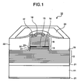
- Fig. 1 is a cross section of a surface-emitting laser element according to a first embodiment of the present invention viewed from an oblique direction;
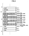
- Fig. 2 is a cross section of a detailed structure near an active layer;
- Fig. 3 is a graph of relaxation-oscillation-frequency dependency of critical back-reflection;
- Fig. 4 is a graph of modulation-doping-amount dependency of critical back-reflection;
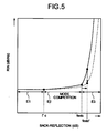
- Fig. 5 is a graph of a change in RIN with respect to the back-reflection;
- Fig. 6 is a graph of a frequency characteristic of RIN;
- Fig. 7 is a graph of reflectance dependency of critical back-reflection with a relaxation oscillation frequency set as a parameter;
- Fig. 8 is a graph of a gain spectrum for explaining detuning in a direction for increasing a differential gain;
- Fig. 9 is a graph of detuning-amount dependency of critical back-reflection; and
- Fig. 10 is a graph of a relation between detuning that occurs in a surface-emitting laser element formed on a wafer and an oscillation wavelength.
-
- 10
- Surface-emitting laser element
- 11
- n-GaAs substrate
- 12
- Lower multilayer mirror
- 13
- Active region
- 14
- Selective oxidation layer
- 15
- Current confinement layer
- 16
- Upper multilayer mirror
- 17
- Contact layer
- 18
- P-side electrode
- 19
- Silicon nitride film
- 20
- Electrode pad
- 21
- n-GaAs buffer layer
- 22
- Polyimide
- 31, 33
- Cladding layers
- 32
- Active layer
- 41a to 41d
- Barrier layers
- 42a to 42c
- Quantum well layers
- λg
- Gain peak wavelength.
- λlasing
- Oscillation wavelength
- L11, L12
- Gain curves
- A surface-emitting laser element and a laser module using the surface-emitting laser element, which are best modes for carrying out the present invention, are explained below.
- A surface-emitting laser element according to a first embodiment is explained. Fig. 1 is a cross section of the surface-emitting laser element according to the first embodiment of the present invention viewed from an oblique direction. In Fig. 1, a surface-emitting
laser element 10 has a structure in which an n-GaAs buffer layer (n=1×1018 cm-3) 21, alower multilayer mirror 12, anactive region 13, anupper multilayer mirror 16 including acurrent confinement layer 15, and acontact layer 17 are stacked on an n-GaAs substrate 11 of a (001) surface one after another, an n-side electrode 21 is provided below the n-GaAs substrate 11, and a ring-shaped p-side electrode 18 and anelectrode pad 20 for leading the p-side electrode 18 are provided above thecontact layer 17. Theactive region 13, theupper multilayer mirror 16, and the p-side electrode 18 form a cylindrical mesa post with the periphery thereof removed. A sidewall of the mesa post and an upper portion of thelower multilayer mirror 12 are covered with asilicon nitride film 19. The periphery of the mesa post is filled with apolyimide 22 via thesilicon nitride film 19. - The
lower multilayer mirror 12 has a structure in which 25.5 pairs of multilayer films with AlAs and GaAs set as a pair are stacked from the n-GaAs substrate 11 side and ten pairs of multilayer films with Al10.9Ga0.1As and GaAs set as a pair are stacked above the 25.5 pairs of multilayer films. Theactive region 13 has anactive layer 32 sandwiched by Claddinglayers active layer 32 forms a multiple quantum well structure of Ga0.63In0.37N0.01As0.974Sb0.016 (a quantum well layer)/GaAs0.93P0.07 (a barrier layer) and has three quantum well layers. Carbon with p=5×1018cm-3 is doped in the barrier layer. Theupper multilayer mirror 16 has a structure in which twenty-three or twenty-six multilayer films with Al0.9Ga0.1As and GaAs set as a pair is stacked. An oscillation wavelength of the surface-emittinglaser element 10 is about 1310 nm. - A method of manufacturing the surface-emitting
laser element 10 is explained. First, the n-GaAs buffer layer (n=1×1018cm-3) 21, thelower multilayer mirror 12, theactive region 13, theupper multilayer mirror 16, and thecontact layer 17 formed of GaAs are stacked on the n-GaAs substrate 11 one after another according to the metal organic chemical vapor deposition (MOCVD) method. Thecurrent confinement layer 15 formed of AlAs with thickness of 20 nm is stacked as a lowermost layer of theupper multilayer mirror 12. - Thereafter, a silicon nitride film is formed on a growing surface of the
contact layer 17 according to the plasma CVD method. A circular pattern with a diameter of about 40 µm to 45 µm is transferred onto the silicon nitride film using the photolithography by a photoresist. The silicon nitride film is etched using the circular resist mask transferred according to the reactive ion etching (RIE) method that uses a CF4 gas. The etching is further performed according to the reactive ion beam etching (RIBE) method that uses a chloride gas until the etching reaches thelower multilayer mirror 12 to form a mesa post of a columnar structure. Depth of the etching by the RIBE method is set to stop the etching in thelower multilayer mirror 12. - In this state, the stacked layers are heated to 400°C in a water vapor atmosphere and left as they are to selectively oxidize the
current confinement layer 15 in the lowermost layer of theupper multilayer mirror 16. Consequently, aselective oxidation layer 14 is formed. A current injection path of thecurrent confinement layer 15 in which theselective oxidation layer 14 is not formed is 3 µm to 10 µm in diameter. Thereafter, after completely removing the silicon nitride film according to the RIE method, the periphery of the mesa post is filled with thepolyimide 22. - Moreover, a silicon nitride film is formed over the entire surface again according to the plasma CVD method. Thereafter, the silicon nitride film in the upper portion of the mesa post is removed in a circular shape. The p-
side electrode 18, which is a ring-shaped AuGeNi/Au electrode, is formed in the portion where the silicon nitride film is removed. Theelectrode pad 20 of Ti/Pt/Au is formed for electrode leading. An area of theelectrode pad 20 is 300 µm2. Thereafter, after grinding the n-GaAs substrate 11 to about 200 µm, the AuGeNi/Au electrode is deposited on the surface of the n-GaAs substrate 11. Finally, the stacked layers are annealed at about 400°C in a nitrogen atmosphere. - Fig. 2 is a diagram of a sectional structure near the
active region 13. As shown in Fig. 2, theactive layer 32 has a triple quantum well structure in which three quantum well layers 42a to 42c made of Ga0.63In0.37N0.01As0.974Sb0.016 with thickness of 7.3 nm are sandwiched among fourbarrier layers 41a to 41d made of GaAs0.93P0.07 with thickness of 15 nm. As described above, carbon with p=5×1018cm-3 is doped in therespective barrier layers 41a to 41d. The Cladding layers 31 and 33 with thickness of 128 nm are provided above and below theactive layer 32. Thickness of each of theupper multilayer mirror 16 and thelower multilayer mirror 12 is λ/4. - In the surface-emitting
laser element 10, it is possible to increase back-reflection tolerance by doping the p-type impurity in the barrier layers 41a to 41d. When there is back-reflection to a semiconductor laser element, a noise level at which noise suddenly increases depends on a characteristic of the semiconductor laser element. In general, a critical back-reflection fextc in an edge emitting laser element is represented by
where τL is a light confinement time of a cavity, Ce is efficiency of coupling with back-reflection at a laser emission end, K is a K factor, fr is a relaxation oscillation frequency, τe is an electron life, and α is a spectral-linewidth enhancement factor. - Increasing the critical back-reflection fextc means increasing back-reflection tolerance. It has been found that, in the case of the surface-emitting laser element, to increase the critical back-reflection fextc without spoiling an optical output, an increase in the relaxation oscillation frequency fr contributes most. Fig. 3 is a diagram of relaxation-oscillation-frequency fr dependency of the critical back-reflection fextc. As shown in Fig. 3, the critical back-reflection fextc increases according to an increase in the relaxation frequency fr. For example, when the relaxation frequency fr is 5 GHz, the critical back-reflection fextc is about -30 dB. When the relaxation frequency fr is increased to 20 GHz, the critical back-reflection fextc increases to about -10 dB. In other words, even if there is back-reflection as large as -10 dB, it is possible to control noise that occurs in the surface-emitting laser element.
- The relaxation oscillation frequency fr has a relation expressed by

- It is possible to realize the increase of the differential gain (dg/dn) by doing an impurity in the barrier layers 41a to 41d of the
active layer 32. Fig. 4 is a graph of modulation-doping-amount dependency of the critical back-reflection fextc. As shown in Fig. 4, when a doping amount in the barrier layers 41a to 41d are increased, the critical back-reflection fextc increases. For example, when the modulation doping amount is changed from p=1×1017cm-3 to p=1×1019cm-3, it is possible to increase the critical back-reflection fextc by about 10 dB.
According to the first embodiment, carbon with p=5×1018cm-3 is doped. - In the surface-emitting
laser element 10 according to the first embodiment, an opening area formed by theselective oxidation layer 14 is 30 µm2. Continuous wave at a threshold current of 1 mA, slope efficiency of 0.3 W/A, and 100°C was obtained. The relaxation oscillation frequency fr in this case was 6 GHz at a bias current of 5 mA when modulation doping for the barrier layers was not performed. The relaxation oscillation frequency fr was successfully increased to 9 GHz by performing the modulation doping. In other words, as shown in Fig. 3, a critical back-reflection was successfully increased from -28 dB to -22 dB. - Back-reflection dependency of relative intensity noise that occurs in the surface-emitting
laser element 10 is considered. As shown in Fig. 5, the RIN increases according to an increase in back-reflection. There are two critical points of the RIN. One critical point is a critical point Γc where mode competition between a cavity mode of the surface-emitting laser element itself and an external cavity mode. The other critical point is a critical point (critical back-reflection) fextc due to coherent collapse. When a distance between the surface-emitting laser element and a reflection point of the back-reflection decreases, the critical point Γc and fextc are closer to each other. The RIN slightly increases when the RIN passes the critical point Γc according to the increase in the back-reflection. The RIN suddenly increases when the RIN passes the critical point fextc. Therefore, it is possible to control occurrence of large RIN by increasing a value of the critical point fextc. In other words, as shown in Fig. 5, when the critical point fextc is changed to a critical point fextc', a characteristic curve of the RIN and the back-reflection is deformed to an increasing side of the back-reflection. Thus, it is possible to expand back-reflection regions E1 and E2 where the value of the RIN is small and increase large back-reflection tolerance. This critical point fextc is the critical back-reflection fextc described above. - Optical communication performed using this surface-emitting laser element is considered. Fig. 6 is a graph of a frequency characteristic of the RIN. As shown in Fig. 6, the RIN takes a large value near the relaxation oscillation frequency fr. In Fig. 6, since the relaxation oscillation frequency fr is 5 GHz, a value of the RIN near the relaxation oscillation frequency fr is large. When transmission speed of the optical communication is about 2 GHz, it is possible to perform communication without being affected by the relaxation oscillation frequency fr. However, when the transmission speed of the optical communication is increased to about 8 GHz, the relaxation oscillation frequency of 5 GHz affects communication as noise. In this case, if the relaxation oscillation frequency is shifted to a relaxation oscillation frequency fr' that exceeds a communication frequency band ER of 0 to 8 GHz and at which noise due to a relaxation oscillation frequency does not affect the communication frequency band EH, a value of the RIN decreases and it is possible to perform satisfactory communication. According to the first embodiment, since the relaxation oscillation frequency is successfully shifted from 6 GHz to 9 GHz, it is possible to hold down a value of the RIN at the time of communication with transmission speed of, for example, about 8 GHz.
- A differential gain is increased by the modulation doping, a relaxation oscillation frequency is increased by the increase in the differential gain, and a value of the RIN is reduced by the increase in the relaxation oscillation frequency. This makes it possible to increase critical back-reflection tolerance.
- A critical back-reflection increases according to the increase in the relaxation oscillation frequency and also increases according to an increase in reflectance of the
upper multilayer mirror 16. Fig. 7 is a graph of dependency on reflectance of a critical back-reflection at the time when a relaxation oscillation frequency is set as a parameter. As shown in Fig. 7, the critical back-reflection not only increases according to the increase in the relaxation oscillation frequency but also increases according to the increase in the reflectance of theupper multilayer mirror 16. The increase in the reflectance means reduction of an output of the surface-emitting laser element. On the other hand, it is not easy to increase an output of the surface-emitting laser element. Therefore, the increase in the relaxation oscillation frequency by the modulation doping makes it possible to increase back-reflection tolerance without decreasing an optical output of the surface-emitting laser element and also makes it possible to perform satisfactory high-speed communication. For example, in Fig. 7, the relaxation oscillation frequency is set to 10 GHz, -24 dB of a critical back-reflection standard for a DFB laser element in the present situation is cleared by setting the reflectance to 0.995 and setting the relaxation oscillation frequency to 10 GHz. - Examples of the surface-emitting laser element subjected to the modulation doping include the following. A surface-emitting laser element in a long wavelength band that has the critical back-reflection fextc, with which a value of the RIN at 0 GHz to 2 GHz becomes -115 dB/Hz, equal to or larger than -30 dB and the relaxation oscillation frequency fr at a bias point equal to or higher than 5 GHz is realized. This makes it possible to satisfactorily perform communication at transmission speed of 2.6 Gbps. A surface-emitting leaser element in a 1.3-µm band that has the critical back-reflection fextc, with which a value of the RIN at 0 GHz to 8 GHz becomes -115 dB/Hz, equal to or larger than -20 dB and the relaxation oscillation frequency fr at a bias point equal to or higher than 10 GHz is realized. This makes it possible to satisfactorily perform communication at transmission speed of 10 Gbps. Moreover, a surface-emitting laser element in a 1.55-µm band that has the critical back-reflection fextc, with which a value of the RIN at 0 GHz to 8 GHz becomes - 115 dB/Hz, equal to or larger than -30 dB and the relaxation oscillation frequency fr at a bias point equal to or higher than 10 GHz is realized. This makes it possible to satisfactorily perform communication at transmission speed of 10 Gbps.
- According to the first embodiment, modulation doping density is p=5×1018cm-3. However, the modulation doping density is preferably set to p=1×1018cm-3 to p=2×1019cm-3. According to the first embodiment, carbon is used as the p-type impurity for performing p--type doping. However, the p-type impurity is not limited to carbon. Be, Zn, Mg, or the like may be used as the p-type impurity. These kinds of materials may be simultaneously used.
- Furthermore, according to the first embodiment, the semiconductor film is used for both the
upper multilayer mirror 16 and thelower multilayer mirror 12. However, the multilayer mirrors are not limited to the semiconductor film. For example, a dielectric film may be used. According to the first embodiment, the lower multilayer mirror is formed by the multilayer films with AlAs/GaAs set as a pair and the upper multilayer mirror is formed by the multilayer films with Al0.9Ga0.1As/GaAs set as a pair. However, it is also possible to form both the multilayer mirrors with multilayer films with AlGaAs/AlGaAs having different Al compositions set as a pair. Moreover, it is also possible to provide gradient composition layers in which compositions are gradually changed may be provided among these respective layers. - Moreover, according to the first embodiment, GaInNAsSb is used as the quantum well layers 42a to 42c. However, a material of the quantum well layers 42a to 42c is not limited to this material. For example, an AlGaInAs semiconductor material, a GaInAsP semiconductor material, an InGaAsSb semiconductor material, a TlGaInAsP semiconductor material, or the like may be used. According to the first embodiment, the
active layer 32 has the quantum well structure. However, theactive layer 32 is not limited to this structure. Theactive layer 32 may have a quantum wire structure or a quantum dot structure. - Furthermore, according to the first embodiment, the surface-emitting laser element is the surface-emitting laser element having an oscillation wavelength of about 1310 nm. However, it is also possible to form a surface-emitting laser element having other oscillation wavelengths, for example, an oscillation wavelength in a 300-nm to 1600-nm band. For example, it is also possible to form a surface-emitting laser element having an oscillation wavelength in an 850-nm band. However, in this case, a quantum well layer is formed of GaAs or AlGaInAs.
- Moreover, according to the first embodiment, back-reflection tolerance of the surface-emitting laser element itself is described. However, the present invention is not limited to this back-reflection tolerance. It is also possible to apply the present invention to back-reflection tolerance with a laser module including this surface-emitting laser element set as a unit. In the laser module, the surface-emitting laser element is bonded to a CAN packet, other plastic packages, or the like. An optical fiber receptacle or a pigtail is attached to the laser module. In this case, since the back-reflection tolerance is high, an optical element such as an isolator does not have to be mounted. Thus, it is possible to realize reduction in cost of the laser module itself.
- When this laser module is set as a unit, since a loss due to coupling of the surface-emitting laser element and an optical fiber is intrinsic, a critical back-reflection decreases in appearance. When the loss due to coupling is about 3 dB, the critical back-reflection increases by a loss of 6 dB from the surface-emitting laser element to the optical fiber and vice versa. As a result, a laser module having a surface-emitting laser element in the long wavelength band that has the critical back-reflection fextc, with which a value of the RIN at 0 GHz to 2 GHz becomes -115 dB/Hz, equal to or larger than -24 dB and the relaxation oscillation frequency fr at a bias point equal to or higher than 5 GHz is realized. This makes it possible to satisfactorily perform communication at transmission speed of 2.5 Gbps. A laser module having a surface-emitting laser element in the 1.3-µm band that has the critical back-reflection fextc, with which a value of the RIN at 0 GHz to 8 GHz becomes -115 dB/Hz, equal to or larger than -14 dB and the relaxation oscillation frequency fr at a bias point equal to or higher than 10 GHz is realized. This makes it possible to satisfactorily perform communication at transmission speed of 10 Gbps. Moreover, a laser module having a surface-emitting laser element in the 1.55-µm band that has the critical back-reflection, with which a value of the RIN at 0 GHz to 8 GHz becomes - 115 dB/Hz, equal to or larger than -24 dB and the relaxation oscillation frequency fr at a bias point equal to or higher than 10 GHz is realized. This makes it possible satisfactorily perform communication at transmission speed of 10 Gbps.
- A second embodiment of the present invention is explained. According to the first embodiment, the modulation doping is applied to the barrier layers 41a to 41d as means for increasing the relaxation oscillation frequency fr. However, according to the second embodiment, detuning is performed to increase a differential gain, whereby the relaxation oscillation frequency fr is increased.
- It is possible to increase the differential gain (dg/dn) of the relaxation oscillation frequency fr shown in Equation (2) not only with the demodulation doping but also with the detuning. Fig. 8 is a graph for explaining an increase in a differential gain by the detuning. In Fig. 8, a gain of a laser light has wavelength dependency and temperature dependency. On a gain curve L11 at the time of a room temperature operation, a gain decreases to a short wavelength side and a long wavelength side with a gain peak wavelength λg1 as a peak. Similarly, on a gain curve L12 at the time of a low temperature operation, a gain decreases to a short wavelength side and a long wavelength side with a gain peak wavelength λg2 as a peak. On the gain curve L12 at the time of the low temperature operation, a high gain is generally obtained compared with the gain curve L11 at the time of the room temperature operation. An oscillation wavelength λ1 is an oscillation wavelength at the time of the room temperature operation and coincides with the gain peak wavelength λg1. An oscillation wavelength λ2 is an oscillation wavelength of oscillation shifted to the short wavelength side by the detuning at the time of the low temperature operation. The oscillation wavelength λ2 may coincide with the gain peak wavelength λg2.
- The detuning according to the second embodiment is different from usual detuning. In the usual detuning, a gain curve is shifted to the long wavelength side at the time of a high temperature operation and an oscillation wavelength is shifted to a high temperature side. However, since respective shift amounts are different, this deviation is corrected to adjust the oscillation wavelength to a high gain state at the time of the high temperature operation. On the other hand, in the detuning according to the second embodiment, unlike the usual detuning, an oscillation wavelength is shifted to the short wavelength side.
- The detuning is defined as a difference Dc between a gain peak wavelength λg and an oscillation wavelength λlasing at the room temperature (Dc=λg-λlasing). In Fig. 8, a gain spectrum L11 at the time of low current inject at the time of the room temperature, a gain spectrum L12 at the time of high current injection, and set oscillation wavelength λlasing1 and λlasing2 at the room temperature are shown. The differential gain (dg/dn) is Δg/Δn at the oscillation wavelength λlasing. As shown in Fig. 8, the differential gain (dg/dn) is larger when the gain peak wavelength λg is set larger than the oscillation wavelength λlasing.
- Fig. 9 is a graph of detuning-amount dependency of the critical back-reflection. As shown in Fig. 9, according to an increase in a detuning amount shifted to the short wavelength side, the critical back-reflection increases. It is possible to obtain critical back-reflection equal to or higher than -30 dB. In particular, when the detuning amount is set as large as 50 nm, it is possible to increase the critical back-reflection to near - 20 dB.
- A surface-emitting laser element, which was the surface-emitting laser element described according to the first embodiment and was not subjected to the modulation doping, was manufactured. In the surface-emitting laser element, barrier layers corresponding to the barrier layers 41a to 41d were formed of GaAs, thickness of the barrier layers was set to 20 nm, a cavity length was adjusted, the oscillation wavelength λlasing at the time of the room temperature operation was set to 1300 nm, and the gain peak wavelength λg was set to 1325 nm. Thickness of the respective multilayer films of the
upper multilayer mirror 16 and thelower multilayer mirror 12 is also adjusted to be λ/4. This surface-emitting laser element has an opening area of 30 µm2 and continuously oscillates at a threshold current of 1.5 mA and slope efficiency of 0.25 W/A. When the detuning to the short wavelength side of +25 nm was performed, the relaxation oscillation frequency fr increased from 6 GHz to 10 GHz. When optical communication of 10 Gbps was actually performed, satisfactory communication was successfully performed without any jitter or the like in an eye pattern. - A result obtained by applying the detuning to a plurality of surface-emitting laser element formed on a wafer using an error in manufacturing is explained. Fig. 10 is a graph for explaining a range of a detuning amount on the wafer. In Fig. 10, a characteristic curve R1 indicates reflectance of the
upper multilayer mirror 16, a characteristic curve R2 indicates reflectance of thelower multilayer mirror 12, and a characteristic curve Rm indicates a geometric mean of theupper multilayer mirror 16 and thelower multilayer mirror 12. A black circle mark indicates a gain peak wavelength at the time of the room temperature operation and an X mark indicates an oscillation wavelength at the time of the room temperature operation. As shown in Fig. 10, the gain peak wavelength is shifted to the short wavelength side as a radius (a distance) from the center of the wafer increases. The oscillation wavelength is shifted to the long wavelength side as the distance from the center of the wafer increases. When the distance from the center of the wafer reaches near 20 mm, reflectance suddenly decreases and, according to the decrease, the surface-emitting laser elements stop oscillating. As described above, a value calculated by subtracting an oscillation wavelength at the time of the room temperature operation from a gain peak wavelength at the time of the room temperature operation is a detuning amount. Thus, in Fig. 10, a largest detuning amount Dcmax is obtained in a surface-emitting laser element placed at a distance from the center of about 3 mm. Therefore, in the surface-emitting laser element in the 1.3-µm band, it is possible to perform the detuning to about 0 nm to 25 nm, or about 0 meV to 20 meV. - The respective surface-emitting laser elements on the wafer are elements in the 1.3-µm band. However, it is possible to apply the detuning to about 0 nm to 35 nm (about 0 meV to 20 meV) to a surface-emitting laser element in the 1.55-µm band. This indicates that a detuning amount (a wavelength) in the 1.3-µm band only has to be converted into energy and set as an energy shift amount. This means that it is possible to apply detuning for causing energy shift of 20 meV to the respective surface-emitting laser element in the 1.3-µm band and the 1.55-µm band.
- The surface-emitting leaser element described above is a surface-emitting laser element in the 1.3-µm band. However, it goes without saying that it is also possible to increase a differential gain by applying the detuning to the short wavelength side to the surface-emitting laser element in the 1.55-µm band and increase a relaxation oscillation frequency to thereby increase back-reflection tolerance.
- For example, a surface-emitting laser element, which was the surface-emitting laser element described according to the first embodiment and was not subjected to the modulation doping, was manufactured. In the surface-emitting laser element, the quantum well layers 42a to 42c were formed of Ga0.55In0.45N0.025As0.945Sb0.03, barrier layers corresponding to the barrier layers 41a to 41d were formed of GaN0.02As0.9Sb0.08, thickness of the quantum well layers and the barrier layers was set to 20 nm, a cavity length was adjusted, and the gain peak wavelength λg at the time of the room temperature operation was set to 1580 nm and the oscillation wavelength λlasing at the time of the room temperature operation was set to 1550 nm. Thickness of the respective multilayer films of the
upper multilayer mirror 16 and thelower multilayer mirror 12 is also adjusted to be λ/4. This surface-emitting laser element has an opening area of 30 µm2 and continuously oscillates at a threshold current of 1.5 mA and slope efficiency of 0.25 W/A. When the detuning to the short wavelength side of +30 nm was performed, the relaxation oscillation frequency fr increased from 6 GHz to 10 GHz. When optical communication of 10 Gbps was actually performed, satisfactory communication was successfully performed without any jitter or the like in an eye pattern. - According to the second embodiment, a differential gain is increased by performing the detuning to the short wavelength side and the relaxation oscillation frequency fr is increased by the increase in the differential gain, whereby a surface-emitting laser element with large back-reflection tolerance is realized without decreasing an output.
- Furthermore, according to the second embodiment, the modulation doping described according to the first embodiment is not applied. However, the modulation doping may be applied according to the second embodiment. This makes it possible to further improve a differential gain and, as a result, realize a surface-emitting laser element with larger back-reflection tolerance without decreasing an output.
- When the detuning according to the second embodiment is applied, for example, a surface-emitting laser element in the long wavelength band that has the critical back-reflection fextc, with which a value of the RIN at 0 GHz to 2 GHz becomes -115 dB/Hz, equal to or larger than -30 dB and the relaxation oscillation frequency fr at a bias point equal to or higher than 5 GHz is realized. This makes it possible to satisfactorily perform communication at transmission speed of 2.5 Gbps. A surface-emitting laser element in the 1.3-µm band that has the critical back-reflection fextc, with which a value of the RIN at 0 GHz to 8 GHz becomes -115 dB/Hz, equal to or larger than -20 dB and the relaxation oscillation frequency fr at a bias point equal to or higher than 10 GHz is realized. This makes it possible to satisfactorily perform communication at transmission speed of 10 Gbps. Moreover, a surface-emitting laser element in the 1.55-µm band that has the critical back-reflection fextc, with which a value of the RIN at 0 GHz to 8 GHz becomes -115 dB/Hz, equal to or larger than -30 dB and the relaxation oscillation frequency fr at a bias point equal to or higher than 10 GHz is realized. This makes it possible to satisfactorily perform communication at transmission speed of 10 Gbps.
- Moreover, according to the second embodiment, the semiconductor film is used for both the
upper multilayer mirror 16 and thelower multilayer mirror 12. However, the multilayer mirrors are not limited to the semiconductor film. For example, a dielectric film may be used. According to the second embodiment, the lower multilayer mirror is formed by the multilayer films with AlAs/GaAs set as a pair and the upper multilayer mirror is formed by the multilayer films with Al0.9Ga0.1As/GaAs set as a pair. However, it is also possible to form both the multilayer mirrors with multilayer films with AlGaAs/AlGaAs having different Al compositions set as a pair. Moreover, it is also possible to provide gradient composition layers in which compositions are gradually changed may be provided among these respective layers. - Furthermore, according to the first embodiment, GaInNAsSb is used as the quantum well layers 42a to 42c. However, a material of the quantum well layers 42a to 42c is not limited to this material. For example, an AlGaInAs semiconductor material, a GaInAsP semiconductor material, an InGaAsSb semiconductor material, a TlGaInAsP semiconductor material, or the like may be used. According to the first embodiment, the
active layer 32 has the quantum well structure. However, theactive layer 32 is not limited to this structure. Theactive layer 32 may have a quantum wire structure or a quantum dot structure. - Moreover, according to the second embodiment, the surface-emitting laser element is the surface-emitting laser element having an oscillation wavelength in the 1310-nm band and the 1550-nm band. However, it is also possible to form a surface-emitting laser element having other oscillation wavelengths, for example, an oscillation wavelength in a 300-nm to 1600-nm band. For example, it is also possible to form a surface-emitting laser element having an oscillation wavelength in an 850-nm band. However, in this case, a quantum well layer is formed of GaAs.
- Furthermore, according to the second embodiment, back-reflection tolerance of the surface-emitting laser element itself is described. However, the present invention is not limited to this back-reflection tolerance. It is also possible to apply the present invention to back-reflection tolerance with a laser module including this surface-emitting laser element set as a unit. In the laser module, the surface-emitting laser element is bonded to a CAN packet, other plastic packages, or the like. An optical fiber receptacle or a pigtail is attached to the laser module. In this case, since the back-reflection tolerance is high, an optical element such as an isolator does not have to be mounted. Thus, it is possible to realize reduction in cost of the laser module itself.
- When this laser module is set as a unit, since a loss due to coupling of the surface-emitting laser element and an optical fiber is intrinsic, a critical back-reflection decreases in appearance. When the loss due to coupling is about 3 dB, in the laser module, the critical back-reflection increases by a loss of 6 dB from the surface-emitting laser element to the optical fiber and vice versa. As a result, a laser module having a surface-emitting laser element in the long wavelength band that has the critical back-refleation fextc, with which a value of the RIN at 0 GHz to 2 GHz becomes -115 dB/Hz, equal to or larger than -24 dB and the relaxation oscillation frequency fr at a bias point equal to or higher than 5 GHz is realized. This makes it possible to satisfactorily perform communication at transmission speed of 2.5 Gbps. A laser module having a surface-emitting laser element in the 1.3-µm band that has the critical back-reflection fextc, with which a value of the RIN at 0 GHz to 8 GHz becomes -115 dB/Hz, equal to or larger than -14 dB and the relaxation oscillation frequency fr at a bias point equal to or higher than 10 GHz is realized. This makes it possible to satisfactorily perform communication at transmission speed of 10 Gbps. Moreover, a laser module having a surface-emitting laser element in the 1.55-µm band that has the critical back-reflection, with which a value of the RIN at 0 GHz to 8 GHz becomes -115 dB/Hz, equal to or larger than -24 dB and the relaxation oscillation frequency fr at a bias point equal to or higher than 10 GHz is realized. This makes it possible satisfactorily perform communication at transmission speed of 10 Gbps.
- According to the first and the second embodiments, the surface-emitting laser element is the surface-emitting laser element formed on the n-type substrate. However, the surface-emitting laser element is not limited to this surface-emitting laser element. The surface laser element may be a surface-emitting laser element formed on a p-type substrate. In this case, the
selective oxidation layer 14 is provided on a p-side, that is, the lower multilayer mirror side and performs current confinement. - As described above, the present invention relates to a vertical cavity surface-emitting laser and, in particular, is useful for a surface-emitting laser element that can improve critical back-reflection tolerance and a laser module using the surface-emitting laser element.
Claims (26)
- A surface-emitting laser element in which a cavity is formed by a lower multilayer mirror and an upper multilayer mirror and an active layer is arranged between the lower multilayer mirror and the upper multilayer mirror, wherein
a relaxation oscillation frequency at a bias point in the cavity is set to exceed an optical communication frequency for modulating a laser light output from the surface-emitting laser element. - The surface-emitting laser element according to claim 1, wherein
the relaxation oscillation frequency is set by increasing a differential gain. - The surface-emitting laser element according to claim 1, wherein
a p-type impurity is doped in a barrier layer forming the active layer. - The surface-emitting laser element according to claim 3, wherein
a concentration of the doping is in a range between 1×1018cm-3 and 2×1019cm-3. - The surface-emitting laser element according to claim 3, wherein
the p-type impurity includes at least one selected from a group consisting of carbon, beryllium, zinc, and magnesium. - The surface-emitting laser element according to claim 1, wherein
in a setting of the relaxation oscillation frequency, a detuning from a gain peak wavelength at a room temperature to an oscillation wavelength at an operation is performed toward a short wavelength side. - The surface-emitting laser element according to claim 7, wherein
a value of the detuning is a value with which at least a differential gain is increased after the detuning. - The surface-emitting laser element according to claim 6, wherein
a value of the detuning is an energy shift value obtained by converting a wavelength into energy and is a value equal to or less than 20 milli-electron volts. - The surface-emitting laser element according to claim 1, wherein
an oscillation frequency is in a range between 300 nanometers and 1600 nanometers. - The surface-emitting laser element according to claim 1, wherein
a selective oxidation layer obtained by oxidizing a part of a current confinement layer containing at least aluminum and arsenide is provided to confine an injection current. - The surface-emitting laser element according to claim 1, wherein
a well layer or a barrier layer forming the active layer uses any one of Gax1In1-x1Ny1Asy2Sb1-y1-y2 (0≤x1, y1, y2≤1), Alx2Gax3In1-x2-x3As (0≤x2, x3≤1), and Tlx4Gax5In1-x4- x5Asy3P1-y3 (0≤x4, x5, y4≤1). - The surface-emitting laser element according to claim 1, wherein
the active layer has any one of a quantum well structure, a quantum wire structure, and a quantum dot structure. - The surface-emitting laser element according to claim 1, wherein
both the upper multilayer mirror and the lower multilayer mirror are semiconductor multilayer films or dielectric multilayer films, or one of the upper multilayer mirror and the lower multilayer mirror is a semiconductor multilayer film and other of the upper multilayer mirror and the lower multilayer mirror is a dielectric multilayer film. - The surface-emitting laser element according to claim 1, wherein
the upper multilayer mirror, the active layer, and the lower multilayer mirror are formed on a gallium arsenide substrate, and
the upper multilayer mirror and the lower multilayer mirror includes a plurality of pairs of multilayer films of Alx6Ga1-x6As (0≤x6<1) and Alx7Ga1-7xAs (0<x7≤1, x6<x7) set as a pair. - The surface-emitting laser element according to claim 1, wherein
a critical back-reflection, with which a value of relative intensity noise becomes -115 decibels per hertz in a region of the optical communication frequency of 0 gigahertz to 2 gigahertz, is equal to or larger than -30 decibels, and
the relaxation oscillation frequency at the bias point is equal to or higher than 5 gigahertz. - The surface-emitting laser element according to claim 1, wherein
a critical back-reflection, with which a value of relative intensity noise becomes -115 decibels per hertz in a region of the optical communication frequency of 0 gigahertz to 8 gigahertz, is equal to or larger than -20 decibels,
the relaxation oscillation frequency at the bias point is equal to or higher than 10 gigahertz, and
an oscillation wavelength is in a 1300-nanoineter band. - The surface-emitting laser element according to claim 1, wherein
a critical back-reflection, with which a value of relative intensity noise becomes -115 decibels per hertz in a region of the optical communication frequency of 0 gigahertz to 8 gigahertz, is equal to or larger than -30 decibels,
the relaxation oscillation frequency at the bias point is equal to or higher than 10 gigahertz, and
an oscillation wavelength is in a 1550-nanometer band. - A laser module comprising:a surface-emitting laser element in which a cavity is formed by a lower multilayer mirror and an upper multilayer mirror and an active layer is arranged between the lower multilayer mirror and the upper multilayer mirror, whereina relaxation oscillation frequency of the surface-emitting laser element at a bias point in the cavity is set to exceed an optical communication frequency for modulating a laser light output from the surface-emitting laser element, andthe laser light emitted from the surface-emitting laser element is output to outside via an optical fiber.
- The laser module according to claim 18, wherein
the relaxation oscillation frequency is set by doping a p-type impurity in a barrier layer forming the active layer to increase a differential gain. - The laser module according to claim 18, wherein
in a setting of the relaxation oscillation frequency, a detuning from a gain peak wavelength at a room temperature to an oscillation wavelength at an operation is performed toward a short wavelength side, and
a value of the detuning is a value with which at least a differential gain is increased after the detuning. - The laser module according to claim 18, further comprising:a CAN-type package.
- The laser module according to claim 18, further comprising:an optical fiber receptacle.
- The laser module according to claim 18, further comprising:an optical fiber pigtail.
- The laser module according to claim 18, wherein
a critical back-reflection, with which a value of relative intensity noise becomes -115 decibels per hertz in a region of the optical communication frequency of 0 gigahertz to 2 gigahertz, is equal to or larger than -30 decibels, and
the relaxation oscillation frequency at the bias point is equal to or higher than 5 gigahertz. - The laser module according to claim 18, wherein
a critical back-reflection, with which a value of relative intensity noise becomes -115 decibels per hertz in a region of the optical communication frequency of 0 gigahertz to 8 gigahertz, is equal to or larger than -20 decibels,
the relaxation oscillation frequency at the bias point is equal to or higher than 10 gigahertz, and
an oscillation wavelength is in a 1300-nanometer band. - The laser module according to claim 18, wherein
a critical back-reflection, with which a value of relative intensity noise becomes -115 decibels per hertz in a region of the optical communication frequency of 0 gigahertz to 8 gigahertz, is equal to or larger than -30 decibels,
the relaxation oscillation frequency at the bias point is equal to or higher than 10 gigahertz, and
an oscillation wavelength is in a 1550-nanometer band.
Applications Claiming Priority (2)
| Application Number | Priority Date | Filing Date | Title |
|---|---|---|---|
| JP2004061258A JP2005252032A (en) | 2004-03-04 | 2004-03-04 | Surface emitting laser device and laser module using the same |
| PCT/JP2005/003612 WO2005086301A1 (en) | 2004-03-04 | 2005-03-03 | Surface-emitting laser element and laser module using same |
Publications (3)
| Publication Number | Publication Date |
|---|---|
| EP1729384A1 true EP1729384A1 (en) | 2006-12-06 |
| EP1729384A8 EP1729384A8 (en) | 2007-03-21 |
| EP1729384A4 EP1729384A4 (en) | 2008-04-16 |
Family
ID=34918053
Family Applications (1)
| Application Number | Title | Priority Date | Filing Date |
|---|---|---|---|
| EP05719916A Withdrawn EP1729384A4 (en) | 2004-03-04 | 2005-03-03 | Surface-emitting laser element and laser module using same |
Country Status (4)
| Country | Link |
|---|---|
| US (1) | US20070030874A1 (en) |
| EP (1) | EP1729384A4 (en) |
| JP (1) | JP2005252032A (en) |
| WO (1) | WO2005086301A1 (en) |
Families Citing this family (21)
| Publication number | Priority date | Publication date | Assignee | Title |
|---|---|---|---|---|
| JP2007103576A (en) * | 2005-10-03 | 2007-04-19 | Furukawa Electric Co Ltd:The | Surface emitting laser module |
| JP2007194561A (en) * | 2006-01-23 | 2007-08-02 | Nec Corp | Surface emitting laser |
| JP2007311632A (en) * | 2006-05-19 | 2007-11-29 | Furukawa Electric Co Ltd:The | Surface emitting laser element |
| JP5027010B2 (en) | 2007-03-01 | 2012-09-19 | 古河電気工業株式会社 | Surface emitting laser element |
| US8144742B2 (en) | 2007-03-01 | 2012-03-27 | Furukawa Electric Co., Ltd. | Surface emitting laser device |
| US8031754B2 (en) * | 2008-04-24 | 2011-10-04 | The Furukawa Electric Co., Ltd. | Surface emitting laser element, surface emitting laser element array, method of fabricating a surface emitting laser element |
| JP5616009B2 (en) | 2008-09-22 | 2014-10-29 | アズビル株式会社 | Reflective photoelectric sensor and object detection method |
| JP2010251698A (en) | 2009-03-27 | 2010-11-04 | Furukawa Electric Co Ltd:The | Surface emitting laser element, surface emitting laser array element, surface emitting laser device, light source device, and optical module |
| JP5659476B2 (en) * | 2009-09-25 | 2015-01-28 | ソニー株式会社 | Correction circuit, drive circuit, and light emitting device |
| JP2011151357A (en) | 2009-12-21 | 2011-08-04 | Ricoh Co Ltd | Optical device, optical scanning apparatus, and image forming apparatus |
| JP5834414B2 (en) | 2010-03-18 | 2015-12-24 | 株式会社リコー | Surface emitting laser module, optical scanning device, and image forming apparatus |
| JP2011249763A (en) * | 2010-04-28 | 2011-12-08 | Ricoh Co Ltd | Light source unit, optical scanner and image forming apparatus |
| JP2012151441A (en) | 2010-12-28 | 2012-08-09 | Ricoh Co Ltd | Optical device, optical scanner, and image formation apparatus |
| WO2013110004A1 (en) * | 2012-01-20 | 2013-07-25 | The Regents Of The University Of California | Short cavity surface emitting laser with double high contrast gratings with and without airgap |
| JP2012156562A (en) * | 2012-05-21 | 2012-08-16 | Nec Corp | Surface emitting laser |
| US9082637B2 (en) | 2012-08-17 | 2015-07-14 | The University Of Connecticut | Optoelectronic integrated circuit |
| JP6012399B2 (en) * | 2012-10-25 | 2016-10-25 | 古河電気工業株式会社 | Optical module |
| KR102276422B1 (en) * | 2014-07-18 | 2021-07-12 | 삼성전자주식회사 | Transmission type high absorption optical modulator and method of manufacturing the same |
| CN105337166B (en) * | 2015-11-30 | 2019-01-11 | 武汉电信器件有限公司 | A kind of molecular beam epitaxy accretion method of high velocity vertical cavity surface emitting lasers |
| CN112393692B (en) * | 2019-08-14 | 2023-04-28 | Oppo广东移动通信有限公司 | Laser projection module, image acquisition module, depth camera and electronic equipment |
| CN119199259B (en) * | 2024-10-30 | 2025-06-20 | 浙江老鹰半导体技术有限公司 | VCSEL chip relaxation oscillation frequency estimation method, device, equipment, medium and program product |
Family Cites Families (13)
| Publication number | Priority date | Publication date | Assignee | Title |
|---|---|---|---|---|
| JP3010817B2 (en) * | 1991-08-22 | 2000-02-21 | 株式会社日立製作所 | Semiconductor optical device |
| JP4362873B2 (en) * | 1998-05-11 | 2009-11-11 | ソニー株式会社 | Semiconductor laser and optical disk apparatus |
| US6368890B1 (en) * | 1999-05-05 | 2002-04-09 | Mitel Semiconductor Ab | Top contact VCSEL with monitor |
| JP2000332341A (en) * | 1999-05-24 | 2000-11-30 | Sony Corp | Semiconductor laser |
| JP2001059923A (en) * | 1999-06-16 | 2001-03-06 | Seiko Epson Corp | Optical module and manufacturing method thereof, semiconductor device, and optical transmission device |
| US7004644B1 (en) * | 1999-06-29 | 2006-02-28 | Finisar Corporation | Hermetic chip-scale package for photonic devices |
| US6653662B2 (en) * | 2000-11-01 | 2003-11-25 | Matsushita Electric Industrial Co., Ltd. | Semiconductor light-emitting device, method for fabricating the same, and method for driving the same |
| US6803604B2 (en) * | 2001-03-13 | 2004-10-12 | Ricoh Company, Ltd. | Semiconductor optical modulator, an optical amplifier and an integrated semiconductor light-emitting device |
| JP2002359434A (en) * | 2001-03-29 | 2002-12-13 | Ricoh Co Ltd | Surface emitting laser element and surface emitting laser array using the surface emitting laser element |
| US7075954B2 (en) * | 2001-05-29 | 2006-07-11 | Nl Nanosemiconductor Gmbh | Intelligent wavelength division multiplexing systems based on arrays of wavelength tunable lasers and wavelength tunable resonant photodetectors |
| JP3981257B2 (en) * | 2001-10-23 | 2007-09-26 | ローム株式会社 | Surface emitting semiconductor laser |
| US6859481B2 (en) * | 2002-07-16 | 2005-02-22 | Applied Optoelectronics, Inc. | Optically-pumped multiple-quantum well active region with improved distribution of optical pumping power |
| KR101168283B1 (en) * | 2005-08-09 | 2012-07-30 | 삼성전자주식회사 | High power vertical external cavity surface emitting laser |
-
2004
- 2004-03-04 JP JP2004061258A patent/JP2005252032A/en active Pending
-
2005
- 2005-03-03 WO PCT/JP2005/003612 patent/WO2005086301A1/en not_active Ceased
- 2005-03-03 EP EP05719916A patent/EP1729384A4/en not_active Withdrawn
-
2006
- 2006-09-05 US US11/515,017 patent/US20070030874A1/en not_active Abandoned
Non-Patent Citations (6)
| Title |
|---|
| NOBUAKI HATORI ET AL: "An Over 10-Gb/s Transmission Experiment Using a p-Type Delta-Doped InGaAs-GaAs Quantum-Well Vertical-Cavity Surface-Emitting Laser" IEEE PHOTONICS TECHNOLOGY LETTERS, IEEE SERVICE CENTER, PISCATAWAY, NJ, US, vol. 10, no. 2, February 1998 (1998-02), XP011045902 ISSN: 1041-1135 * |
| OTSUKA N ET AL: "1.5-[mu]m strained-layer MQW-DFB lasers with high relaxation-oscillation frequency and low-chirp characteristics" IEEE JOURNAL OF QUANTUM ELECTRONICS IEEE USA, vol. 32, no. 7, July 1996 (1996-07), pages 1230-1236, XP002471747 ISSN: 0018-9197 * |
| See also references of WO2005086301A1 * |
| SEKI S ET AL: "Theoretical analysis of differential gain of 1.55 [mu]m InGaAsP/InP compressive-strained multiple-quantum-well lasers" JOURNAL OF APPLIED PHYSICS USA, vol. 75, no. 3, 1 February 1994 (1994-02-01), pages 1299-1303, XP002471748 ISSN: 0021-8979 * |
| SUNDGREN P ET AL: "High-performance 1.3 µm InGaAs vertical cavity surface emitting lasers" ELECTRONICS LETTERS, IEE STEVENAGE, GB, vol. 39, no. 15, 24 July 2003 (2003-07-24), pages 1128-1129, XP006020692 ISSN: 0013-5194 * |
| UOMI K ET AL: "MODULATION-DOPED MULTI-QUANTUM WELL (MD-MQW) LASERS. II. EXPERIMENT" JAPANESE JOURNAL OF APPLIED PHYSICS, JAPAN SOCIETY OF APPLIED PHYSICS, TOKYO, JP, vol. 29, no. 1, PART 1, January 1990 (1990-01), pages 88-94, XP000102156 ISSN: 0021-4922 * |
Also Published As
| Publication number | Publication date |
|---|---|
| EP1729384A8 (en) | 2007-03-21 |
| JP2005252032A (en) | 2005-09-15 |
| US20070030874A1 (en) | 2007-02-08 |
| WO2005086301A1 (en) | 2005-09-15 |
| EP1729384A4 (en) | 2008-04-16 |
Similar Documents
| Publication | Publication Date | Title |
|---|---|---|
| US20070030874A1 (en) | Surface-emitting laser element and laser module using the same | |
| US6890778B2 (en) | Vertical cavity surface emitting laser and a method of fabrication thereof | |
| EP1378039B1 (en) | Vertical cavity surface emitting laser | |
| Park et al. | Low-threshold oxide-confined 1.3-μm quantum-dot laser | |
| EP1389813B1 (en) | Wavelength tunable VCSEL | |
| US6144682A (en) | Spatial absorptive and phase shift filter layer to reduce modal reflectivity for higher order modes in a vertical cavity surface emitting laser | |
| US6674778B1 (en) | Electrically pumped edge-emitting photonic bandgap semiconductor laser | |
| US20020163950A1 (en) | Coupled cavity anti-guided vertical-cavity surface-emitting laser | |
| US20170005455A1 (en) | Tunable optical phase filter | |
| US6011811A (en) | Buried heterostructure with aluminum-free active layer and method of making same | |
| WO2002049171A9 (en) | Laser diode with nitrogen incorporating barrier | |
| EP3890127B1 (en) | Vcsel with increased wavelength dependence on driving current | |
| US7816163B2 (en) | Radiation-emitting semiconductor body for a vertically emitting laser and method for producing same | |
| US6924161B2 (en) | Protective side wall passivation for VCSEL chips | |
| EP0660472A2 (en) | Semiconductor laser device | |
| US20080232417A1 (en) | Semiconductor light emitting device and fabrication method for semiconductor light emitting device | |
| Cheng et al. | Lasing characteristics of high-performance narrow-stripe InGaAs-GaAs quantum-well lasers confined by AlAs native oxide | |
| US5953358A (en) | Semiconductor laser device | |
| US10516251B2 (en) | Reliable high-speed oxide-confined vertical-cavity surface-emitting laser | |
| JP2006019470A (en) | Surface emitting semiconductor laser and optical module | |
| JP2002111125A (en) | Distributed feedback semiconductor laser | |
| US11362486B2 (en) | High speed high bandwidth vertical-cavity surface-emitting laser with controlled overshoot | |
| CN1868099A (en) | Surface-emitting semiconductor laser comprising a structured waveguide | |
| Ries et al. | Visible‐spectrum (λ= 650 nm) photopumped (pulsed, 300 K) laser operation of a vertical‐cavity AlAs–AlGaAs/InAlP–InGaP quantum well heterostructure utilizing native oxide mirrors | |
| US6795469B2 (en) | Semiconductor laser element |
Legal Events
| Date | Code | Title | Description |
|---|---|---|---|
| PUAI | Public reference made under article 153(3) epc to a published international application that has entered the european phase |
Free format text: ORIGINAL CODE: 0009012 |
|
| 17P | Request for examination filed |
Effective date: 20060904 |
|
| AK | Designated contracting states |
Kind code of ref document: A1 Designated state(s): DE GB |
|
| RAP1 | Party data changed (applicant data changed or rights of an application transferred) |
Owner name: THE FURUKAWA ELECTRIC CO., LTD. |
|
| RIN1 | Information on inventor provided before grant (corrected) |
Inventor name: CASIMIRUS, SETIAGUNG,THE FURUKAWA ELECTRIC CO. L Inventor name: IWAI, NORIHIRO,THE FURUKAWA ELECTRIC CO., LTD. Inventor name: SHIMIZU, HITOSHI,THE FURUKAWA ELECTRIC CO., LTD. Inventor name: KOYAMA, FUMIO Inventor name: ARIGA, MAIKO,THE FURUKAWA ELECTRIC CO., LTD. Inventor name: ARAI, MASAKAZU |
|
| RIN1 | Information on inventor provided before grant (corrected) |
Inventor name: ARIGA, MAIKO,THE FURUKAWA ELECTRIC CO., LTD. Inventor name: CASIMIRUS, SETIAGUNG,THE FURUKAWA ELECTRIC CO. L Inventor name: KOYAMA, FUMIO Inventor name: IWAI, NORIHIRO,THE FURUKAWA ELECTRIC CO., LTD. Inventor name: ARAI, MASAKAZU Inventor name: SHIMIZU, HITOSHI,THE FURUKAWA ELECTRIC CO., LTD. |
|
| RIN1 | Information on inventor provided before grant (corrected) |
Inventor name: IWAI, NORIHIRO,THE FURUKAWA ELECTRIC CO., LTD. Inventor name: ARIGA, MAIKO,THE FURUKAWA ELECTRIC CO., LTD. Inventor name: ARAI, MASAKAZUPHOTONICS DEVICE LABORATORY Inventor name: SHIMIZU, HITOSHI,THE FURUKAWA ELECTRIC CO., LTD. Inventor name: KOYAMA, FUMIO Inventor name: CASIMIRUS, SETIAGUNG,THE FURUKAWA ELECTRIC CO. L |
|
| DAX | Request for extension of the european patent (deleted) | ||
| RBV | Designated contracting states (corrected) |
Designated state(s): DE GB |
|
| A4 | Supplementary search report drawn up and despatched |
Effective date: 20080319 |
|
| 17Q | First examination report despatched |
Effective date: 20081201 |
|
| STAA | Information on the status of an ep patent application or granted ep patent |
Free format text: STATUS: THE APPLICATION IS DEEMED TO BE WITHDRAWN |
|
| 18D | Application deemed to be withdrawn |
Effective date: 20090415 |