EP1729199A1 - Method for improving the data transfer in semi synchronous clock domains integrated circuits at any possible m/n clock ratio - Google Patents
Method for improving the data transfer in semi synchronous clock domains integrated circuits at any possible m/n clock ratio Download PDFInfo
- Publication number
- EP1729199A1 EP1729199A1 EP06011147A EP06011147A EP1729199A1 EP 1729199 A1 EP1729199 A1 EP 1729199A1 EP 06011147 A EP06011147 A EP 06011147A EP 06011147 A EP06011147 A EP 06011147A EP 1729199 A1 EP1729199 A1 EP 1729199A1
- Authority
- EP
- European Patent Office
- Prior art keywords
- data transfer
- clock
- frequency
- faster
- circuits
- Prior art date
- Legal status (The legal status is an assumption and is not a legal conclusion. Google has not performed a legal analysis and makes no representation as to the accuracy of the status listed.)
- Granted
Links
Images





Classifications
-
- G—PHYSICS
- G06—COMPUTING OR CALCULATING; COUNTING
- G06F—ELECTRIC DIGITAL DATA PROCESSING
- G06F1/00—Details not covered by groups G06F3/00 - G06F13/00 and G06F21/00
- G06F1/04—Generating or distributing clock signals or signals derived directly therefrom
- G06F1/12—Synchronisation of different clock signals provided by a plurality of clock generators
-
- H—ELECTRICITY
- H04—ELECTRIC COMMUNICATION TECHNIQUE
- H04L—TRANSMISSION OF DIGITAL INFORMATION, e.g. TELEGRAPHIC COMMUNICATION
- H04L7/00—Arrangements for synchronising receiver with transmitter
- H04L7/02—Speed or phase control by the received code signals, the signals containing no special synchronisation information
Definitions
- the present invention relates, in general, to a method for data transfer between semi synchronous clock circuits and, more specifically, for synchronizing two semi synchronous clock domains.
- the invention also relates to a data transfer system which comprises a Generic Frequency Converter for data exchange between two integrated processors or circuits in a System on Chip based on a synchronous interconnection protocol.
- SoC System on Chip
- these specific methods provide that the clock generator subsystem, for each synchronizer instantiated within the SoC, generates, routes and calibrates some control signals needed to store of some informations, for instance regarding the frequency ratio and other characteristics of the clock signals which are necessary for a correct data exchange.
- Such methods exploit conventional dual port RAM or other unconventional FIFO buffers (dual port based methods) where only two stage buffers are used, one of which being synchronous to the faster clock and the other to the slower clock.
- Such methods are based on the specific relationship of the two involved clocks, driving the swap of data from the input buffer to the output one in order to sinchronize data.
- a dual port RAM inevitably introduces some delay because of the need for the synchronization of the read and write ports that work at different frequencies.
- the technical problem underlying the present invention is that of providing a method and a corresponding system for improving data transfer in semi synchronous clock domain circuits and for synchronizing two semi synchronous clock domains according to a systematic approach without introducing latencies that drammatically reduce the throughput of the system and without using buffering techniques for storing data not ready to be processed.
- the solution idea on the basis of the present invention is to provide a method to know "a priori" a maximum possible data rate for a specific ratio m/n taking into account all the possible timing loss sources present in an interconnection line, thus providing a useful tool that stresses the constraints to be guaranteed in order to achieve a desired data rate, the method supporting a designer about the actual possibility to synthetize devices or integrated circuits on the basis of specific project parameters in order, not only to foresee the performance, but also to verify the feasibility of the synthetization phase.
- a method for synchronizing two semi synchronous clock domains for data transfer comprising the following phases: a) analysis, for each frequency ratio under test, to know a maximum possible data transfer rate as a function of all the possible input and output delays that may be tolerated, depending on critical technological parameters; b) providing a Generic Frequency Converter between a couple of integrated processors or circuits for data exchange that may be programmed for each frequency ratio m/n; c) configuring at least a scheduler for driving the data transfer.
- the method proposed works at the faster clock frequency and acts only on the communication (bus) control signals in such a way to schedule the transfer operation phases, in order to allow a reliable exchange for each frequency ratio m/n ( ⁇ 1), with the maximum possible data transfer rate and without the use of buffers.
- the present invention allows to introduce specific constraints in each case under study in order to supply the design engineer with an easy way to customize his design, with the view to matching the particular requirements of the case under test, in an easy and flexible way.
- SoC System on Chip
- Faster IP two integrated processors or circuits
- Slower IP each working with a corresponding clock signal Faster_clock with a frequency f faster and Slower_ lock with a frequency f slower , respectively.
- R F m / n ( ⁇ 1) be the clock frequencies ratio, with m and n integers with no common integer divider but one. This frequency constraint assures a periodic relationship between the rising edges of the two clock signals.
- this period will be referred to as synchronization period T s.
- T s the two clock signals are aligned.
- a Synch signal is supposed high for a Faster_clock cycle (being in such high logic level in a last cycle within the synchronization period Ts ), as shown in fig.3.
- T R T S 2 m n
- time resolution T R is used to derive:
- Tsu a Set up Time of the system
- the Set up Time T SU is the time required for the bus control signals to propagate from faster integrated processor or circuit to the slower one.
- p f and p s are two parameters generally ranging in [0, ⁇ ) which establish respectively how many Faster_clock and Slower_clock periods are required for signal propagation.
- Eq.1 may be replaced by: ⁇ m i n ⁇ + 1 ⁇ m i n ⁇ p f m n + p s
- ⁇ t i states when a set up time violation occurs for transfer operations generated by the Slower IP which begins in that cycle.
- Eq.2 may be rearranged as follows: ⁇ n j m ⁇ + 1 ⁇ n j m ⁇ p s n m + p f
- SIR Slower IP Ready to receive
- control signal generators 4 and 5 are responsible to know the state, cycle after cycle, of the three events (SUTV_F, SUTV_S and SIR) that are necessary to schedule a correct data transfer from a clock domain to another.
- the two control signal generators 4 and 5 By means of the Synch signal only, which is the unique signal requested to be generated by the clock generator subsystem, the two control signal generators 4 and 5 generate within the synchronization period Ts the correct sequences of the three events and output them as three control signals that drive the operation of the frequency conversion logics of the GFC.
- control signal generators 4 and 5 are capable of generating the correct sequence for the three events according to the constraints imposed by the specific application and they are also programmable by the design engineer in order to accommodate different frequencies ratios or ratios changing on the fly.
- control signals generator that produces the signals needed to correctly exchange data by means of the Up frequency converter logic is composed of three word generators.
- a block scheme of the control signal generator and of its interface is shown in figure 6.
- the up_EVENT_val signals are the preset signals and define the state of the particular event of interest for which realizing the timing sequence, in the i th cycle of the faster frequency clock within the synchronization period Ts.
- the up_EVENT_val[i] signal defines the event state in the i th cycle of Faster_clock within the synchronization period Ts and it is programmed according to the Set up time T su of the system which has been fixed for the implementation.
- An external block for instance one of the two integrated processor or circuit, provides these signals to the GFC and maintain them stable for the entire working time.
- the number n max is the maximum number among all the n i of the pre-defined set of frequency ratios.
- the integer i is such that 2 i is the smallest interger power of 2 that contains n max (2 (i-1) ⁇ n max ⁇ 2 i ). If the current frequency ratio that has to be managed is m k /n k then the current value of the mux_ctrl_signals must be set to n k -1.
- Word generators are realized by means of few building blocks connected in cascade. To implement a GFC that manages the set of frequency ratios m1/n1, m2/n2, ..., the number of the building blocks instantiated for implementing a word generator is determined by n max . All this is done for making the word generator flexible for managing different frequency ratios which may be dynamically changed during the working of the system.
- a multiplexer is implemented, which is needed to select the output of the flip flop whose output represents the desired control signal.
- the feedback from the output of the multiplexer to the input of the Block 4 (Block n max -1 in a general case) is useful if the synchronization or Synch signal is suddenly lost and it guarantees the correct operation of the generator in any way.
- the multiplexer dimensions (fan-in) is the smallest one that is capable of distinguishing among n max inputs, that is the fan in of the multiplexer is the smallest power of two that contains n max . All the other inputs are, for convenience, connected to the output of the Block 0.
- the control signals of the multiplexer are provided by the same integrated processor or circuit which the preset signals come from and they establish the output of the flip-flop that represents the control signal to be realized.
- the control signals of the multiplexer determine the current frequency ratio that the GFC has to handle. As said above, if m k /n k is the current frequency ratio of the pre-defined set of frequency ratios to be managed, then n k -1 is the value to be set for the control signals of the multiplexer.
- next[i] is reported to the output reg[i] of the flip flop.
- the current value of the next[i] signal is selected by the Synch signal. If the Synch signal is '0' then next[i] is equal to reg[i+l] signal, which is the output of the previous block of the word generator, while if the Synch is '1' next[i] is equal to up_val[i], which is the preset signal that comes from a block external to the GFC.
- the method according to the present invention solves the problem of data synchronization between two integrated processors or circuits working with semi-synchronous clock signals, automatically exploring the design space and implementation parameters.
- the present invention also relates to a definition and an implementation of a software platform capable of reducing as much as possible all practical issues in designing a generic synchronization device.
- EVENT_val signals that program the schedulers for the communication. For reliable transaction and for transaction with a given date transfer rate only well defined values are allowed, which are function of Set Up time of the system and of the constraints imposed by the application.
- the method according to the present invention provides for design space exploration, for example relating to design constraints (frequency ratio, faster clock, etc.) and to planning scheduling ( EVENT_val's ) and synthesis parameters.
- Such method interfaces to the synthesis system in such a way as reducing as much as possible front-end design time.
- the method according to the present invention is capable to provide with a high degree of confidence information on the possibility of synthesizing the device when design constraints and output parameters are given.
- the flow chart of the design platform operations and its interface to the synthesis tool is depicted in figure 9.
- the input parameters of the development platform are: the frequencies ratio (m, n), the Faster_clock ( f faster ), the maximum clocks skew (clks_skew), the GFC critical path ( bridge_delay ) and the resolution step ( resolution ), whose meaning will be made clear later on.
- the output parameters are the values for correctly programming the schedulers ( EVENT_val's ) and a script file which is imported into the synthesis tool.
- the method comprises three logical steps: simulation, output of the EVENT_val's and generation of a script file to be imported in a synthesis tool.
- the Set Up time of the system Tsu has been defined for convenience as the sum of two parts which are expressed for convenience as multiplies of clock periods.
- Two parameters ( p f and p s ) establish the weight that each part has in determining the Set Up time T su , which is the overall delay needed to safely communicate a signal generated by one integrated processor or circuit to the other one.
- this time consists of different delays, which are:
- the time p f T f is assumed to be composed of the propagation delay from faster IP interface to GFC interface, the faster IP clock-to-out delay (or faster IP set up time if the acknowledgement signal is considered) and the critical path delay of the GFC. It is worth to note that this last delay is a constant for a given implementation technology.
- the time p f T f may be considered as the sum of two parts one of which is a constant.
- p f del f + C
- C is a constant which depends on the process to be used for implementation
- del f is the fraction of T f which takes into account the delay from Faster IP interface to GFC interface and the faster IP clock-to-out delay (or Faster IP set up time if the acknowledgement signal is considered).
- the sum of these two last delays will be referred to as input (or output) delay for signals which are in the faster domain.
- the parameters del f and del s provide the user with the maximum possible values of input and output delays of the bus control signals that can be tolerated when implementing the synchronization device.
- the parameters del f and del s have an important role in the synthesis process and, therefore, they are correctly estimated in order to support the design engineer for developing projects employing the GFC. Setting the input parameters in a the simulator, it is possible to estimate with a high level of confidence the maximum input and output delays which may be set to the GFC input and output signals in all the possible situations in the synthesis process.
- Eqq. 1', 2' and 3' have been obtained by taking into account the two clock signals as if they were ideal and an elaboration time of GFC that was negligible, for practical evaluation of del f and del s also the clocks skew and the GFC delay are to be considered.
- the effect of real clocks and GFC delay may be considered as a loss in ⁇ t i and ⁇ t i with respect to an ideal case.
- the losses due to GFC propagation delay and clock uncertainties are strictly dependent on the maximum frequency, and they have been modelled by means of an empirical rule which linearly depends on the maximum frequency; the losses which are encountered for data flow generated by the integrated processor or circuit in the faster clock domain path may be modelled as: clks_skew + bridge_delay ⁇ f faster while the losses in the slower clock domain are: clks_skew ⁇ f faster ⁇ m n
- the simulators outputs other useful information which may facilitate the configuration of the synthesis parameters and indicate with high degree of confidence the possibility of synthesizing the block.
- the resolution step chosen for del f and del s is 5% of T f and T s .
- the method according to the present invention allows a design engineer to know "a priori" the value of the transfer data rate related to the input and output delays that may be guaranteed in the particular context of study.
- the table in figure 11 is related to the data flow generated by the Slower integrated processor or circuit and it has been obtained by applying for the losses the following equations: clock_skew + bridge_delay ⁇ f faster ⁇ m n clock_skew ⁇ f faster
- the equation 6 is applied to the slower domain and the equation 7 to the faster one.
- the inspection of the Table in figure 11 is analogous to that of Table 10.
- the design engineer has to start its choice by first selecting the input and output delays of the signal related to the slower clock domain in the column of the table and then follows the same procedure explained above to select the input and output delays of the signals related to the faster clock domain, in order to obtain the desired transfer rate.
- the proposed simulators provide for the user to set the constraints del f and del s which allow to obtain the desired transfer rate.
- constraints del f and del s which allow to obtain the desired transfer rate.
- the method according to the present invention also comprises an interface for generating a script file to be imported in a traditional synthesis tool.
- a script generator outputs a text file and alerts for any constraints configuration which is not compatible to correct data transfers and the metastability issues. Part of a script file generated in a case under test is schematically reported in figure 13.
- FIGS 14 and 15 show the down frequency conversion logic and the up frequency conversion block scheme.
- knowing "a priori" the possibility to synthetize, under a particular parameters selection and relatively to a given context, is particularly relevant when a system on chip comprises a plurality of devices, the synthetization being carried out by automatically and without further analysis on the context.
- the method improve the time and cost needed to syntetize the entire system on chip.
- this method overcomes the limits of the classical theories by a means of an approach that maintains the generality of the methodology that uses a dual port RAM but eliminatig the high impact in area and latency of which this standard technique soffers.
- the method of the invention do not introduce latencies and high area consumption compared to other methods dealing with data synchronization according to a philosophy that solves a specific frequency ratio in a specific and well defined scenario.
- the present invention also relates to a system for data transfer between two semi synchronous clock domains in a System on Chip, the system including at least corresponding first and second integrated processors or circuits respectively working at a first and a second frequency clock.
- the system comprises detection means for detecting, at each frequency ratio between the first and second frequency clock, a maximum rate of the data transfer.
- the data rate is a function of all the possible input and output delays supported by the System on Chip, depending on a plurality of technological parameters.
- the system also comprises a scheduler for driving the data transfer between the semi synchronous clock domains and a Generic Frequency Converter between the first and the second integrated processors or circuits for the data transfer.
- the system improves data transfer in semi synchronous clock domains including at least two integrated processors or circuits of a System on Chip based on a synchronous interconnection protocol.
- the system provides "a priori" a maximum possible data rate for a specific ratio m/n in order to exchange only the supported data for that specific ratio, programs correctly a scheduler that drives transfer operation and then provides a generic frequency converter between the integrated processors or circuits for data exchange, for each frequency ratio m/n according to the results of the previous phases.
Landscapes
- Engineering & Computer Science (AREA)
- Theoretical Computer Science (AREA)
- Physics & Mathematics (AREA)
- General Engineering & Computer Science (AREA)
- General Physics & Mathematics (AREA)
- Information Transfer Systems (AREA)
Abstract
Description
- The present invention relates, in general, to a method for data transfer between semi synchronous clock circuits and, more specifically, for synchronizing two semi synchronous clock domains.
- The invention also relates to a data transfer system which comprises a Generic Frequency Converter for data exchange between two integrated processors or circuits in a System on Chip based on a synchronous interconnection protocol.
- As it is well known in this specific technical field, the complexity of the System on Chip (SoC) designs is rising inexorably, with a concomitant increase in the number of integrated processors or circuits (IPs) working with different clock frequencies signals. Therefore, the SoC design strategy brings the problem to arrange an efficient interaction between separate processors or circuits in order to obtain also the maximum possible data transfer rate, with low impact on area.
- In literature, the problem of synchronizing two semi synchronous integrated processors or circuits (IPs) in a SoC and its various solutions are widely documented.
- At least in principle, it is possible to design a specific method supporting a correct data exchange between two semi synchronous clock integrated processors or circuits that work with respective frequency having a well defined ratio m/n.
- A few methods to synchronize semi-synchronous domains are known in literature for specific frequency ratios, each of which exploits an "ad hoc" simple circuitry to solve synchronization issues related to data exchange. However, these solutions are not susceptible for handling all possible frequency ratios m/n.
- Moreover, these specific methods often require several signals that must be generated by a clock generation subsystem in order to drive reliable transfers, further increasing post-layout simulation for chip validation.
- In fact, these specific methods provide that the clock generator subsystem, for each synchronizer instantiated within the SoC, generates, routes and calibrates some control signals needed to store of some informations, for instance regarding the frequency ratio and other characteristics of the clock signals which are necessary for a correct data exchange.
- For these reasons, it is expensive, at least in term of time and resources, to use such methods to synchronize semi-synchronous domains not only because they do not manage in a flexible and general way all the frequency ratios (thus solving the synchronization problem in a systematic and automatic way) but also because they requires a device having a high impact on the clock generator subsystem and on the area of the SoC as a whole.
- On the other hand, in the specific literature a few methods exist that solve the problem of providing a synchronization according to a systematic approach and without loading the clock generator subsystem.
- Such methods exploit conventional dual port RAM or other unconventional FIFO buffers (dual port based methods) where only two stage buffers are used, one of which being synchronous to the faster clock and the other to the slower clock.
- Such methods are based on the specific relationship of the two involved clocks, driving the swap of data from the input buffer to the output one in order to sinchronize data.
- Other similar methods exploit a double input buffer to reduce transfer latency and similarly swap the data to output buffer, avoiding metastability issues.
- However, methods that insure data synchronization by using a dual port RAM have the disadvatage of introducing large latencies that drammatically reduce the throughput of the system.
- According to the prior art, a dual port RAM inevitably introduces some delay because of the need for the synchronization of the read and write ports that work at different frequencies.
- This issue is partially solved in a method based on dual port RAM when a data stream is sent but an intrinsic delay remains when communication is burst. In fact, one datum always needs at least two clock cycles to be transmitted.
- Moreover, a method that uses a FIFO (with two or more stages) to buffer a wide data bus, as those generally present in a SoC, is inevitably much more area consuming and this may be a critical aspect that leads to limit as much as possible this solutions.
- At the state of the art, it is not known a synchronization method able to guarantee the maximum possible data transfer for each frequency ratio m/n, without introducing latencies for improper data-rate exchange and with a low impact on the clock generator subsystem and on the area.
- More particularly, it is not known a method managing only the bus communication control signals in a selective way while respecting the timing constraints imposed by the two involved integrated processors or circuits, by the wires buses, by the clocks frequencies and by the constraints of the technology implemented for the system.
- The technical problem underlying the present invention is that of providing a method and a corresponding system for improving data transfer in semi synchronous clock domain circuits and for synchronizing two semi synchronous clock domains according to a systematic approach without introducing latencies that drammatically reduce the throughput of the system and without using buffering techniques for storing data not ready to be processed.
- The solution idea on the basis of the present invention is to provide a method to know "a priori" a maximum possible data rate for a specific ratio m/n taking into account all the possible timing loss sources present in an interconnection line, thus providing a useful tool that stresses the constraints to be guaranteed in order to achieve a desired data rate, the method supporting a designer about the actual possibility to synthetize devices or integrated circuits on the basis of specific project parameters in order, not only to foresee the performance, but also to verify the feasibility of the synthetization phase.
- On the base of such solution idea, the technical problem is solved by a method for synchronizing two semi synchronous clock domains for data transfer comprising the following phases: a) analysis, for each frequency ratio under test, to know a maximum possible data transfer rate as a function of all the possible input and output delays that may be tolerated, depending on critical technological parameters; b) providing a Generic Frequency Converter between a couple of integrated processors or circuits for data exchange that may be programmed for each frequency ratio m/n; c) configuring at least a scheduler for driving the data transfer.
- More particularly, the method proposed, works at the faster clock frequency and acts only on the communication (bus) control signals in such a way to schedule the transfer operation phases, in order to allow a reliable exchange for each frequency ratio m/n (<1), with the maximum possible data transfer rate and without the use of buffers.
- In order to reach the purpose of the invention, few critical parameters are considered, which are strictly related to the silicon integration process and required for the device implementation.
- The present invention allows to introduce specific constraints in each case under study in order to supply the design engineer with an easy way to customize his design, with the view to matching the particular requirements of the case under test, in an easy and flexible way.
- The features and advantages of the method of the present invention will be apparent from the following description of an embodiment thereof given by way of non-limiting example with reference to the attached drawings.
-
- Figure 1 shows a simplified and schematic representation of a prior art system for synchronizing semi-synchronous domains.
- Figure 2 shows a simplified and schematic representation of an architecture of a Generic Frequency Converter of a data transfer system according to the present invention.
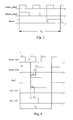
- Figure 3 shows the synchronization period Ts and the timing of the synchronization signal according to the present invention when the two clocks have a frequency ratio of 2/3.
- Figure 4 shows, in a simplified and schematic representation, a Set up time of the system in two different cases and the timing constraints that insure no set up time violations for data which is sent by a faster integrated processor or circuit toward a slower one.
- Figure 5 shows, in a simplified and schematic representation, the timing sequence of the event SIR within the synchronization period T S .
- Figure 6 shows a simplified and schematic representation of the Up control signals generator scheme according to the present invention.
- Figure 7 shows, in a simplified and schematic representation, an example of control signal generator according to the present invention.
- Figure 8 shows a simplified and schematic representation of the ith building block of word generators according to the present invention.
- Figure 9 shows a flow chart of the design environment of the method according to the present invention.
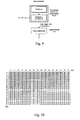
- Figure 10 shows a table representing the data transfer rates generated by a faster clock according to the present invention.
- Figure 11 shows a table representing the data transfer rates generated by a slower clock according to the present invention.
- Figure 12 shows a table representing an example of the preset values elaborated by the design tool according to the present invention.
- Figure 13 shows a fragment of the file script output of the design tool according to the present invention, which acts as interface with a standard synthesis tool.
- Figure 14 shows, in a simplified and schematic representation, the down frequency converter according to the present invention.
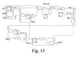
- Figure 15 shows, in a simplified and schematic representation, the up frequency converter according to the present invention.
- With reference to the drawing's view, and specifically to the example of Figure 2, is globally and schematically shown with numeral reference 1a Generic Frequency Converter according to the present invention, which is inserted between a couple of processor or circuits for data exchange.
- For correctly understanding the principles and the rules which the Generic Frequency Converter is based and implemented on, few considerations about the data transfer rate are made.
- Let's first consider a System on Chip (SoC) including two integrated processors or circuits, hereafter referred as a Faster IP and a Slower IP, each working with a corresponding clock signal Faster_clock with a frequency f faster and Slower_ lock with a frequency f slower, respectively.
- Let R F = m / n (≤ 1) be the clock frequencies ratio, with m and n integers with no common integer divider but one. This frequency constraint assures a periodic relationship between the rising edges of the two clock signals. Hereafter, for brevity, this period will be referred to as synchronization period Ts. Furthermore, for simplicity it is assumed that after each synchronization period Ts the two clock signals are aligned.
- According to these assumptions, within the synchronization period T S, n cycles of the Faster_clock and m cycles of Slower_clock occur, as schematically shown in figure 3 for m=2 and n=3. Within the synchronization period Ts, all the phase relationships that occur between the rising edges of the two clock signals are present, and they periodically repeat every synchronization period Ts.
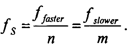
- In order to establish when the clock signals are aligned, a Synch signal is supposed high for a Faster_clock cycle (being in such high logic level in a last cycle within the synchronization period Ts), as shown in fig.3. As a consequence, the frequency fs̅ of the Sync signal is
- Starting from this hypothesis, it's possible to mathematically demonstrate that we must keep memory of only three events for correct data transfer from one integrated processor or circuit to the other one.
- Specifically, we must keep memory of the event which indicates the set up time violations for the signals forwarded by the faster integrated processor or circuit toward the slower one, the event which indicates the set up time violations for the signals forwarded by the slower integrated processor or circuit toward the faster one and finally the event which says when the slower integrated processor or circuit samples the data
- Thus, it is possible to demonstrate that these three events are just the only ones that we must take into consideration for correctly transferring data. Let Ts=1/fs=n/f faster =m/f slower be the synchronisation period.
- To know the instant when the positive edges of the two clocks are within the synchronization period Ts, a time resolution T R, which is the maximum common divider between the semi-periods of the clocks and, is defined as:

- More particularly, the time resolution T R is used to derive:
- The Faster_Clock period T faster, which is given by T faster =2mT R
- The Slower_Clock period T slower, which is given by T slower =2nT R
- The i th rising edge of the Faster_Clock within the the synchronization period Ts occurs at t i rf =2imT R (0≤ i<n);
- The j th rising edge of the Slower_Clock within the the synchronization period Ts occurs at t j rs =2jnT R (0≤j<m);
- In order to allow correct data communication, a Set up Time of the system, Tsu, is defined as follows:

- In other words, the Set up Time T SU is the time required for the bus control signals to propagate from faster integrated processor or circuit to the slower one. p f and p s are two parameters generally ranging in [0, ∞) which establish respectively how many Faster_clock and Slower_clock periods are required for signal propagation.
- More generally, if the bus is full duplex, with the buses having different lengths and characteristics, two Set up Times are defined, one for the command bus and one for the response bus.
- Let us now assume that the Faster IP starts an action at time


where i is the index indicating the period of the Faster_clock within the synchronization period T s . - Therefore, a data transmission which begins at the time instant


- For each i within the synchronization period T S, Eq.1 states when a set up time violation occurs for transfer operations generated by the Faster IP and beginning in that cycle, as depicted in figure 4. It is easy to verify that no set up time violation occurs in the case (a) shown in fig.4, while for an action which starts in the same cycle (i=1) when a different Set up Time T su is defined for the system (case b) no correct data transfer is possible.
- After easy calculations, Eq.1 may be replaced by:

- In the same way, let us assume that the Slower IP starts an action at time


where j is the index indicating the period of the Slower_clock within the synchronization period T s. Therefore, a data transmission which begins at the time instant


- For each j within the synchronization period Ts, Δt i states when a set up time violation occurs for transfer operations generated by the Slower IP which begins in that cycle. Eq.2 may be rearranged as follows:

- In the following, we will refer to these two events as SUTV_F and SUTV_S for the Set Up Time Violation for the signals forwarded by the Faster IP and Set Up Time Violation for signals forwarded by the Slower IP, respectively.
- The event which indicates the sampling of the request by the Slower IP or the sampling of the Ack signal when response data flow is considered occurs when:

- Eq.3 becomes:

- In the following, we will refer to this event as Slower IP Ready to receive (SIR). As it can be noted in the last relationship, this event never occurs for i=0 and always for i=n-1 when m / n ≤1. An example of SIR event is shown in figure 5 for the
frequency ratio 2/3, where the positive logic level indicates the sampling by the slower integrated processor or circuit. - Supposing that no transfer operation is pending, if the faster integrated processor or circuit starts an action at time

- 1. If SIR='1' and SUTV_F='0' at cycle i, directly connecting the Faster IP to the Slower one, and vice versa: in this situation signals coming from the IPs must not be elaborated in any way (Req_f=Req_s='1' and Ack_f=Ack_s='1'). In this case the operation ends in the same cycle i.
- 2. If SIR='0' and SUVT_F='0' at cycle i, the Req_f signal must be forwarded to the Slower IP with no elaboration, while the bridge must filter the Ack_s signal; in following cycles:
- · Req_s must maintain the logic level which Req_f had in the previous cycle;
- · Ack_s must be forbidden until the cycle k (k>i) in which SIR='1' and Req_f[k+1]='1'; at the end of this cycle, the action started at time ti rf completes;
- 3. If neither the case 1) nor the case 2) occur at cycle i, all the Slower and Faster IP signals must be filtered; all this, provided that we are not serving the situation 2).
- Now, let us suppose that the Slower IP starts an action at time tj rs (0≤j< m) within Ts, and that no pending requests are present. Note that the time t j rs (0≤ j< m) is always inside a cycle i of the faster clock but at the beginning of the synch period. The situations that may occur are:
- 1. SUTV_S='0' at the cycle i; in this case up conversion logic must always forward the request to the Faster IP and maintain it until the Faster IP samples it, that is until the end of the cycle; in the next cycles the signal must be forbidden. This is the starting point of the operation. Req_f='0' otherwise.
- 2. If SUTV_S='0' at the cycle i, then starting from this cycle, the actions of the GFC are identical to what explained for data exchange requested by the Faster IP.
- Note that it is possible to complete an operation in the same cycle which it is requested in, only if the cycle is the last of the synchronization period, for example only if Synch signal is at high logic level;
- The above considerations outline the importance of knowing the state, cycle after cycle, of the three events (SUTV_F, SUTV_S and SIR) that are necessary to schedule a correct data transfer from a clock domain to another.
- According to the present invention,
control signal generators - By means of the Synch signal only, which is the unique signal requested to be generated by the clock generator subsystem, the two
control signal generators - The
control signal generators - When two different data buses are encountered, each of which with its own length and constraints, accordingly two schedulers could be necessary, one for driving the down conversion logic and another for the up conversion, as reported in Fig.2.
- In fact, even if the two blocks use the same events it is possible to separate the implementation of the two buses and to match the requirements and constraints of a single frequency conversion block without conditioning the data transfer rate of the other one. Nevertheless, only one control signals generator (scheduler) may be used if the two buses have the same constraints.
- Here the implementation of the only Up control signal generator is described.
- More particularly, the control signals generator that produces the signals needed to correctly exchange data by means of the Up frequency converter logic is composed of three word generators. A block scheme of the control signal generator and of its interface is shown in figure 6.
- The up_EVENT_val signals are the preset signals and define the state of the particular event of interest for which realizing the timing sequence, in the ith cycle of the faster frequency clock within the synchronization period Ts.
- The up_EVENT_val[i] signal defines the event state in the i th cycle of Faster_clock within the synchronization period Ts and it is programmed according to the Set up time T su of the system which has been fixed for the implementation. An external block, for instance one of the two integrated processor or circuit, provides these signals to the GFC and maintain them stable for the entire working time.
- To implement a GFC that manages the set of frequency ratios m1/n1, m2/n2, ..., then the number nmax is the maximum number among all the ni of the pre-defined set of frequency ratios.
- The integer i is such that 2i is the smallest interger power of 2 that contains nmax (2(i-1)< nmax ≤2i). If the current frequency ratio that has to be managed is mk/nk then the current value of the mux_ctrl_signals must be set to nk-1.
- Word generators are realized by means of few building blocks connected in cascade. To implement a GFC that manages the set of frequency ratios m1/n1, m2/n2, ..., the number of the building blocks instantiated for implementing a word generator is determined by nmax. All this is done for making the word generator flexible for managing different frequency ratios which may be dynamically changed during the working of the system.
- In the figure 7 an example of a word generator in the case nmax=5 (for handling frequency ratios equal to m/5 with 1≤m<5) is reported.
- As it is schematically shown in figure 7, for each word generator, a multiplexer is implemented, which is needed to select the output of the flip flop whose output represents the desired control signal. The feedback from the output of the multiplexer to the input of the Block 4 (Block nmax-1 in a general case) is useful if the synchronization or Synch signal is suddenly lost and it guarantees the correct operation of the generator in any way.
- The multiplexer dimensions (fan-in) is the smallest one that is capable of distinguishing among nmax inputs, that is the fan in of the multiplexer is the smallest power of two that contains nmax. All the other inputs are, for convenience, connected to the output of the
Block 0. - The control signals of the multiplexer (mux_ctrl_signals) are provided by the same integrated processor or circuit which the preset signals come from and they establish the output of the flip-flop that represents the control signal to be realized.
- The control signals of the multiplexer determine the current frequency ratio that the GFC has to handle. As said above, if mk/nk is the current frequency ratio of the pre-defined set of frequency ratios to be managed, then nk-1 is the value to be set for the control signals of the multiplexer.
- In figure 8 the ith building block of the word generators is schematically represented. On every rising edge of the clock signal, the next[i] value is reported to the output reg[i] of the flip flop. The current value of the next[i] signal is selected by the Synch signal. If the Synch signal is '0' then next[i] is equal to reg[i+l] signal, which is the output of the previous block of the word generator, while if the Synch is '1' next[i] is equal to up_val[i], which is the preset signal that comes from a block external to the GFC.
- Advantageously, the method according to the present invention solves the problem of data synchronization between two integrated processors or circuits working with semi-synchronous clock signals, automatically exploring the design space and implementation parameters.
- The present invention, also relates to a definition and an implementation of a software platform capable of reducing as much as possible all practical issues in designing a generic synchronization device.
- In fact, the correct sequence within the synchronization period Ts of events SUTV_F, SUTV_S and SIR which depend on the specific frequency ratio under study and on the constraint given by the Set up time T su is crucial for a correct data transfer.
- The values of these events are defined by EVENT_val signals that program the schedulers for the communication. For reliable transaction and for transaction with a given date transfer rate only well defined values are allowed, which are function of Set Up time of the system and of the constraints imposed by the application.
- Moreover, when designing a complex integrated system, different options are possible in the placement and routing of different integrated processors or circuits, in such a way as to possibly obtain different values for p f and p s. Therefore, it is of primary importance to study from a rather general point of view the dependence of the maximum transfer rate on p f and p s.
- More particularly, it is necessary to find within which limits p f and p s may be chosen in order to obtain a given transfer rate, provided certain constraints on the propagation delays resulting from floor-planning limitations.
- In this case, it is necessary to know "a priori" what pairs of values p f and p s, if any, may guarantee the desired transfer data rate, and vice versa.
- More generally, it is necessary to implement a method which automatically allows the design engineer to configure the GFC for a specific application under study.
- Advantageously, the method according to the present invention provides for design space exploration, for example relating to design constraints (frequency ratio, faster clock, etc.) and to planning scheduling (EVENT_val's) and synthesis parameters.
- Moreover, such method interfaces to the synthesis system in such a way as reducing as much as possible front-end design time.
- Advantageously, the method according to the present invention is capable to provide with a high degree of confidence information on the possibility of synthesizing the device when design constraints and output parameters are given. The flow chart of the design platform operations and its interface to the synthesis tool is depicted in figure 9.
- The input parameters of the development platform are: the frequencies ratio (m, n), the Faster_clock (f faster), the maximum clocks skew (clks_skew), the GFC critical path (bridge_delay) and the resolution step (resolution), whose meaning will be made clear later on. The output parameters are the values for correctly programming the schedulers (EVENT_val's) and a script file which is imported into the synthesis tool.
- The method comprises three logical steps: simulation, output of the EVENT_val's and generation of a script file to be imported in a synthesis tool.
- The Set Up time of the system Tsu has been defined for convenience as the sum of two parts which are expressed for convenience as multiplies of clock periods. Two parameters (p f and p s) establish the weight that each part has in determining the Set Up time T su , which is the overall delay needed to safely communicate a signal generated by one integrated processor or circuit to the other one.
- More particularly, this time consists of different delays, which are:
- the time after which the signals generated by an integrated processor or circuit may be considered stable at its interface (clock-to-out);
- the wires bus delay;
- the GFC propagation delay;
- the set up time imposed by the receiver interface.
- Hence, the time p f T f is assumed to be composed of the propagation delay from faster IP interface to GFC interface, the faster IP clock-to-out delay (or faster IP set up time if the acknowledgement signal is considered) and the critical path delay of the GFC. It is worth to note that this last delay is a constant for a given implementation technology.
- Therefore, the time p f T f may be considered as the sum of two parts one of which is a constant. In order to take into consideration this fact, let us put:

where C is a constant which depends on the process to be used for implementation, and del f is the fraction of T f which takes into account the delay from Faster IP interface to GFC interface and the faster IP clock-to-out delay (or Faster IP set up time if the acknowledgement signal is considered). Hereafter, the sum of these two last delays will be referred to as input (or output) delay for signals which are in the faster domain. - At the same way, the timing component p s T s can be considered as it is composed of the bus propagation delay in slower domain and of the Slower IP set up time (or clock-to-out, if we consider the request signal). Accordingly, let us put:

where del s is the sum of these two delays and it will be indicated as input (or output) delay for signal in the slower clock domain. - In sum, the parameters del f and del s provide the user with the maximum possible values of input and output delays of the bus control signals that can be tolerated when implementing the synchronization device.
- The parameters del f and del s have an important role in the synthesis process and, therefore, they are correctly estimated in order to support the design engineer for developing projects employing the GFC. Setting the input parameters in a the simulator, it is possible to estimate with a high level of confidence the maximum input and output delays which may be set to the GFC input and output signals in all the possible situations in the synthesis process.
- Because Eqq. 1', 2' and 3' have been obtained by taking into account the two clock signals as if they were ideal and an elaboration time of GFC that was negligible, for practical evaluation of del f and del s also the clocks skew and the GFC delay are to be considered. The effect of real clocks and GFC delay may be considered as a loss in Δt i and Δt i with respect to an ideal case.
- More particularly, the losses due to GFC propagation delay and clock uncertainties are strictly dependent on the maximum frequency, and they have been modelled by means of an empirical rule which linearly depends on the maximum frequency; the losses which are encountered for data flow generated by the integrated processor or circuit in the faster clock domain path may be modelled as:

while the losses in the slower clock domain are:
- The result of simulators elaboration, schematically represented in Figures 10 and 11, provide the values of the transfer rate, expressed as a fraction of the slower clock frequency, as a function of the maximum possible values of input and output delays (delf and dels) of the signals of the GFC which may be tolerated.
- Moreover, the simulators outputs other useful information which may facilitate the configuration of the synthesis parameters and indicate with high degree of confidence the possibility of synthesizing the block.
- Tables in figures 10 and 11, represent a result obtained through an embodiment of the present invention in case of frequency ratio with m=2 and n=3, with the hypothesis that the maximum frequency involved is 300 MHz, the clocks skew is 0.22 ns and the elaboration time of the GFC is 0.6 ns.
- More particularly, the resolution step chosen for delf and dels is 5% of Tf and Ts.
- As it may be seen in figure 10, related to the data flow generated by the Faster integrated processor or circuit, on the first horizontal line the maximum possible values of input and output delays delf of the signals related to the faster clock domain (Req_f and Ack_f) are reported.
- In the same way, on the vertical axis, in the first column, there are reported the maximum possible values of the input and output delays dels of the signals related to the slower clock domain (Req_s and Ack_s).
- For all pairs of the parameters delf and dels the theoretical values of the maximum transfer data rate, which are expressed as a percentage of the slower clock frequency involved, are shown. Advantageously, the method according to the present invention allows a design engineer to know "a priori" the value of the transfer data rate related to the input and output delays that may be guaranteed in the particular context of study.
- Vice versa, if the requirements are much more directed to the certainty of a particular value of transfer rate, by means of the table in figure the design engineer is able to directly read the input and output delays values which have to be respected for achieving this goal.
- The table in figure 11 is related to the data flow generated by the Slower integrated processor or circuit and it has been obtained by applying for the losses the following equations:


- The
equation 6 is applied to the slower domain and theequation 7 to the faster one. The inspection of the Table in figure 11 is analogous to that of Table 10. In this case the design engineer has to start its choice by first selecting the input and output delays of the signal related to the slower clock domain in the column of the table and then follows the same procedure explained above to select the input and output delays of the signals related to the faster clock domain, in order to obtain the desired transfer rate. - The proposed simulators provide for the user to set the constraints del f and del s which allow to obtain the desired transfer rate. When these constraints have been defined, it is necessary to generate the values for the events SUTV_F, SUTV_S and SIR within T S which insure the correct scheduling operations in the case under study with the given assumptions.
- Advantageously, after defining the two parameters delf and dels, either for the down converter or for the up converter, according to the constraints and requirements of the particular scenario of study, all that we need in order to program the EVENT_val [i] values for each control signals is obtained.
- In fact, the design engineer only set as input parameters the constraints that have been selected from the tables described above (dels and delf, either for the down converter or for the up converter) and the method according to the invention allows to output these values in further tables.
- The table in figure 12 reports for simplicity the results of the elaboration of the tool for the up converter logic in the case m=2, n=3 with the assumptions resolution=5%, f faster=300 MHz, clks_skew=0.2 ns, bridge_delay=0.6 ns, delf=25% and dels=25%.
- The method according to the present invention also comprises an interface for generating a script file to be imported in a traditional synthesis tool.
- A script generator outputs a text file and alerts for any constraints configuration which is not compatible to correct data transfers and the metastability issues. Part of a script file generated in a case under test is schematically reported in figure 13.
- Figures 14 and 15 show the down frequency conversion logic and the up frequency conversion block scheme.
- The advantages achieved through the method according to the present invention are multiple:
- data transfer in semi synchronous clock domains circuit are flexible, general and systematic;
- acting only on a communication control signals only (Request and Grant) and without the use of data buffers, overcoming of traditional synchronization issues due to dual port RAM or dual port based method;
- setting and feasibly changing a few critical parameters, constraints and some other parameters of the technological process that are used for implementing the device;
- alerting a design engineer about the actual possibility to synthetize devices or integrated circuits on the basis of particular project parameters, that is the very same parameters set by the design engineer during the simulation phase.
- In this way a design engineer not only may foresee the performance but also verify the feasibility of synthetization phase. Even if the method of the present invention is based on a deterministic approach, while the rule for establishng the synthetizability is a statistic one in standard synthesis tools, the method according to the present invention guarantees a good level of accuracy.
- In fact, knowing "a priori" the possibility to synthetize, under a particular parameters selection and relatively to a given context, is particularly relevant when a system on chip comprises a plurality of devices, the synthetization being carried out by automatically and without further analysis on the context. The method improve the time and cost needed to syntetize the entire system on chip.
- Advantageously, this method overcomes the limits of the classical theories by a means of an approach that maintains the generality of the methodology that uses a dual port RAM but eliminatig the high impact in area and latency of which this standard technique soffers.
- Advantageously, the method of the invention do not introduce latencies and high area consumption compared to other methods dealing with data synchronization according to a philosophy that solves a specific frequency ratio in a specific and well defined scenario.
- Moreover, it solves the problem of synchronization for all frequency ratios in all the possible scenarios, giving to the design engineer the possibility of setting the most critical parameters for the synthesis and verifying all the possible maximum data rate as a function of the input and output delays of the control signals of the synchronous bus protocol.
- The present invention also relates to a system for data transfer between two semi synchronous clock domains in a System on Chip, the system including at least corresponding first and second integrated processors or circuits respectively working at a first and a second frequency clock.
- More particularly, the system comprises detection means for detecting, at each frequency ratio between the first and second frequency clock, a maximum rate of the data transfer.
- The data rate is a function of all the possible input and output delays supported by the System on Chip, depending on a plurality of technological parameters.
- More particularly, the system also comprises a scheduler for driving the data transfer between the semi synchronous clock domains and a Generic Frequency Converter between the first and the second integrated processors or circuits for the data transfer.
- Advantageously, the system improves data transfer in semi synchronous clock domains including at least two integrated processors or circuits of a System on Chip based on a synchronous interconnection protocol.
- In fact, the system provides "a priori" a maximum possible data rate for a specific ratio m/n in order to exchange only the supported data for that specific ratio, programs correctly a scheduler that drives transfer operation and then provides a generic frequency converter between the integrated processors or circuits for data exchange, for each frequency ratio m/n according to the results of the previous phases.
Claims (8)
- Method for data transfer between two semi synchronous clock domains in a System on Chip including at least a first and second integrated processors or circuits, respectively working at a first and a second frequency clock, characterized by comprising the phase of:a) detecting, for each frequency ratio between said first and second frequency clock, a maximum rate of said data transfer;b) programming a frequency conversion between said first and second integrated processors or circuits for said data transfer;c) scheduling said data transfer between said first and second integrated processors or circuits.
- Method according to claim 1 characterized in that said maximum rate is a function of all the possible input and output delays supported by said System on Chip.
- Method according to claim 2 characterized in that said function takes into account a plurality of technological parameters of said System on Chip.
- Method according to claim 1 characterized by comprising means to alert a human user about the synthetizability of said System on Chip on the basis of an output of said function.
- Method according to claim 1 characterized in that said phase of programming said frequency conversion includes the steps of:- generating within a synchronization period sequences of events;- converting said sequences of events in corresponding control signals;- driving said frequency conversion according to said corresponding control signals.
- Method according to claim 5 characterized in that said sequences of events and control signals are sequences of three events and three control signals.
- Method according to claim 6 characterized in that said control signals comprises the step of generating at least a word through a plurality of building blocks connected in cascade, a number of said building blocks in cascade being depending on a higher frequency between said first and said second frequency clock.
- Data transfer system between two semi synchronous clock domains in a System on Chip including at least a first and second integrated processors or circuits respectively working at a first and a second frequency clock, characterized by comprising:- detection means for detecting, at each frequency ratio between said first and second frequency clock, a maximum rate of said data transfer, said rate being a function of all the possible input and output delays supported by said System on Chip, depending on a plurality of technological parameters;- a scheduler, driving said data transfer between said semi synchronous clock domains;- a Generic Frequency Converter between said first and second integrated processors or circuits for said data transfer.
Priority Applications (1)
| Application Number | Priority Date | Filing Date | Title |
|---|---|---|---|
| EP06011147A EP1729199B1 (en) | 2005-05-31 | 2006-05-31 | Method for improving the data transfer in semi synchronous clock domains integrated circuits at any possible M/N clock ratio |
Applications Claiming Priority (2)
| Application Number | Priority Date | Filing Date | Title |
|---|---|---|---|
| EP05011697 | 2005-05-31 | ||
| EP06011147A EP1729199B1 (en) | 2005-05-31 | 2006-05-31 | Method for improving the data transfer in semi synchronous clock domains integrated circuits at any possible M/N clock ratio |
Publications (2)
| Publication Number | Publication Date |
|---|---|
| EP1729199A1 true EP1729199A1 (en) | 2006-12-06 |
| EP1729199B1 EP1729199B1 (en) | 2010-05-19 |
Family
ID=35056977
Family Applications (1)
| Application Number | Title | Priority Date | Filing Date |
|---|---|---|---|
| EP06011147A Not-in-force EP1729199B1 (en) | 2005-05-31 | 2006-05-31 | Method for improving the data transfer in semi synchronous clock domains integrated circuits at any possible M/N clock ratio |
Country Status (3)
| Country | Link |
|---|---|
| US (1) | US7676685B2 (en) |
| EP (1) | EP1729199B1 (en) |
| DE (1) | DE602006014327D1 (en) |
Families Citing this family (5)
| Publication number | Priority date | Publication date | Assignee | Title |
|---|---|---|---|---|
| US20080005402A1 (en) * | 2006-04-25 | 2008-01-03 | Samsung Electronics Co., Ltd. | Gals-based network-on-chip and data transfer method thereof |
| EP2026493A1 (en) * | 2007-08-16 | 2009-02-18 | STMicroelectronics S.r.l. | Method and systems for mesochronous communications in multiple clock domains and corresponding computer program product |
| GB2484295A (en) * | 2010-10-05 | 2012-04-11 | St Microelectronics Ltd | Circuit simulation |
| US9143315B2 (en) * | 2013-10-25 | 2015-09-22 | Advanced Micro Devices, Inc. | Predictive periodic synchronization using phase-locked loop digital ratio updates |
| FR3134462B1 (en) * | 2022-04-12 | 2024-11-08 | St Microelectronics Rousset | Method for transferring data between a first digital domain and a second digital domain, and corresponding system on chip. |
Citations (5)
| Publication number | Priority date | Publication date | Assignee | Title |
|---|---|---|---|---|
| WO1999019785A1 (en) * | 1997-10-10 | 1999-04-22 | Rambus Incorporated | Apparatus and method for generating a distributed clock signal using gear ratio techniques |
| US20020196886A1 (en) * | 2001-06-22 | 2002-12-26 | Adkisson Richard W. | SYNC pulse compensation and regeneration in a clock synchronizer controller |
| EP1347355A1 (en) * | 2002-03-22 | 2003-09-24 | STMicroelectronics S.r.l. | Frequency converter for interconnect buses |
| US20040223564A1 (en) | 2003-05-09 | 2004-11-11 | Adkisson Richard W. | Programmable clock synchronizer |
| US20040236979A1 (en) * | 2000-06-30 | 2004-11-25 | Wilcox Jeffrey R. | Method and apparatus for an integrated circuit having flexible-ratio frequency domain cross-overs |
Family Cites Families (4)
| Publication number | Priority date | Publication date | Assignee | Title |
|---|---|---|---|---|
| US5634041A (en) * | 1992-08-12 | 1997-05-27 | Massachusetts Institute Of Technology | Rationally clocked communication interface |
| SG47976A1 (en) * | 1994-05-10 | 1998-04-17 | Intel Corp | Method and apparatus for providing synchronous data transmission between digital devices operating at frequencies having a p/q integer ratio relationship |
| US5909563A (en) * | 1996-09-25 | 1999-06-01 | Philips Electronics North America Corporation | Computer system including an interface for transferring data between two clock domains |
| US7100065B2 (en) * | 2003-05-09 | 2006-08-29 | Hewlett-Packard Development Company, L.P. | Controller arrangement for synchronizer data transfer between a core clock domain and bus clock domain each having its own individual synchronizing controller |
-
2006
- 2006-05-31 DE DE602006014327T patent/DE602006014327D1/en not_active Expired - Fee Related
- 2006-05-31 EP EP06011147A patent/EP1729199B1/en not_active Not-in-force
- 2006-05-31 US US11/421,306 patent/US7676685B2/en not_active Expired - Fee Related
Patent Citations (5)
| Publication number | Priority date | Publication date | Assignee | Title |
|---|---|---|---|---|
| WO1999019785A1 (en) * | 1997-10-10 | 1999-04-22 | Rambus Incorporated | Apparatus and method for generating a distributed clock signal using gear ratio techniques |
| US20040236979A1 (en) * | 2000-06-30 | 2004-11-25 | Wilcox Jeffrey R. | Method and apparatus for an integrated circuit having flexible-ratio frequency domain cross-overs |
| US20020196886A1 (en) * | 2001-06-22 | 2002-12-26 | Adkisson Richard W. | SYNC pulse compensation and regeneration in a clock synchronizer controller |
| EP1347355A1 (en) * | 2002-03-22 | 2003-09-24 | STMicroelectronics S.r.l. | Frequency converter for interconnect buses |
| US20040223564A1 (en) | 2003-05-09 | 2004-11-11 | Adkisson Richard W. | Programmable clock synchronizer |
Also Published As
| Publication number | Publication date |
|---|---|
| US20060271806A1 (en) | 2006-11-30 |
| US7676685B2 (en) | 2010-03-09 |
| DE602006014327D1 (en) | 2010-07-01 |
| EP1729199B1 (en) | 2010-05-19 |
Similar Documents
| Publication | Publication Date | Title |
|---|---|---|
| US7290075B2 (en) | Performing arbitration in a data processing apparatus | |
| US8726219B2 (en) | Analysis of digital circuits with time division multiplexing | |
| US8286025B1 (en) | Selection of port adapters for clock crossing boundaries | |
| US7904859B2 (en) | Method and apparatus for determining a phase relationship between asynchronous clock signals | |
| US8290725B2 (en) | Synchronized reconfiguration of measurement modules | |
| Muttersbach | Globally-asynchronous locally-synchronous architectures for VLSI systems | |
| KR20120056255A (en) | Pseudo-synchronous time division multiplexing | |
| Bhadra et al. | A low power UART design based on asynchronous techniques | |
| JP2008532169A (en) | Electronic device and method for arbitrating shared resources | |
| JPWO2006030904A1 (en) | Semiconductor device and communication control method | |
| US8225259B1 (en) | Apparatus and methods for time-multiplex field-programmable gate arrays with multiple clocks | |
| JP2001016234A (en) | CAN controller and one-chip computer with built-in CAN controller | |
| EP2098969A1 (en) | Logic circuit designing device for asynchronous logic circuit, logic circuit designing method, and logic circuit designing program | |
| EP1729199B1 (en) | Method for improving the data transfer in semi synchronous clock domains integrated circuits at any possible M/N clock ratio | |
| US6961691B1 (en) | Non-synchronized multiplex data transport across synchronous systems | |
| JP2012099921A (en) | Circuit and method for data transfer with clock domain crossing | |
| Mekie et al. | Interface design for rationally clocked GALS systems | |
| WO2024066950A1 (en) | Signal processing method, signal processing apparatus, chip, and electronic device | |
| KR100734521B1 (en) | IP Module for System-on-Chip | |
| US20260126827A1 (en) | Adjusted-frequency synchronizer for clock domain crossing | |
| JP5057509B2 (en) | Behavioral synthesis apparatus, behavioral synthesis method, semiconductor integrated circuit manufacturing method, behavioral synthesis program, and readable storage medium | |
| Srihari et al. | A Novel Serial Peripheral Interface Master Core | |
| Mekie et al. | Interfaces for Rationally clocked Globally Asynchronous Locally Synchronous (GALS) systems | |
| Chakraborty et al. | Interfaces for Rationally clocked Globally Asynchronous Locally Synchronous (GALS) systems | |
| JP4817688B2 (en) | Semiconductor integrated circuit device |
Legal Events
| Date | Code | Title | Description |
|---|---|---|---|
| PUAI | Public reference made under article 153(3) epc to a published international application that has entered the european phase |
Free format text: ORIGINAL CODE: 0009012 |
|
| AK | Designated contracting states |
Kind code of ref document: A1 Designated state(s): AT BE BG CH CY CZ DE DK EE ES FI FR GB GR HU IE IS IT LI LT LU LV MC NL PL PT RO SE SI SK TR |
|
| AX | Request for extension of the european patent |
Extension state: AL BA HR MK YU |
|
| 17P | Request for examination filed |
Effective date: 20070524 |
|
| 17Q | First examination report despatched |
Effective date: 20070709 |
|
| AKX | Designation fees paid |
Designated state(s): DE FR GB IT |
|
| GRAP | Despatch of communication of intention to grant a patent |
Free format text: ORIGINAL CODE: EPIDOSNIGR1 |
|
| RAP1 | Party data changed (applicant data changed or rights of an application transferred) |
Owner name: STMICROELECTRONICS SRL |
|
| GRAS | Grant fee paid |
Free format text: ORIGINAL CODE: EPIDOSNIGR3 |
|
| GRAA | (expected) grant |
Free format text: ORIGINAL CODE: 0009210 |
|
| AK | Designated contracting states |
Kind code of ref document: B1 Designated state(s): DE FR GB IT |
|
| REG | Reference to a national code |
Ref country code: GB Ref legal event code: FG4D |
|
| REF | Corresponds to: |
Ref document number: 602006014327 Country of ref document: DE Date of ref document: 20100701 Kind code of ref document: P |
|
| PLBE | No opposition filed within time limit |
Free format text: ORIGINAL CODE: 0009261 |
|
| STAA | Information on the status of an ep patent application or granted ep patent |
Free format text: STATUS: NO OPPOSITION FILED WITHIN TIME LIMIT |
|
| 26N | No opposition filed |
Effective date: 20110222 |
|
| PG25 | Lapsed in a contracting state [announced via postgrant information from national office to epo] |
Ref country code: DE Free format text: LAPSE BECAUSE OF NON-PAYMENT OF DUE FEES Effective date: 20101201 |
|
| PGFP | Annual fee paid to national office [announced via postgrant information from national office to epo] |
Ref country code: FR Payment date: 20110621 Year of fee payment: 6 |
|
| PGFP | Annual fee paid to national office [announced via postgrant information from national office to epo] |
Ref country code: GB Payment date: 20120426 Year of fee payment: 7 |
|
| PGFP | Annual fee paid to national office [announced via postgrant information from national office to epo] |
Ref country code: IT Payment date: 20120424 Year of fee payment: 7 |
|
| REG | Reference to a national code |
Ref country code: FR Ref legal event code: ST Effective date: 20130131 |
|
| PG25 | Lapsed in a contracting state [announced via postgrant information from national office to epo] |
Ref country code: FR Free format text: LAPSE BECAUSE OF NON-PAYMENT OF DUE FEES Effective date: 20120531 |
|
| GBPC | Gb: european patent ceased through non-payment of renewal fee |
Effective date: 20130531 |
|
| PG25 | Lapsed in a contracting state [announced via postgrant information from national office to epo] |
Ref country code: IT Free format text: LAPSE BECAUSE OF NON-PAYMENT OF DUE FEES Effective date: 20130531 |
|
| PG25 | Lapsed in a contracting state [announced via postgrant information from national office to epo] |
Ref country code: GB Free format text: LAPSE BECAUSE OF NON-PAYMENT OF DUE FEES Effective date: 20130531 |