JP2008532169A - Electronic device and method for arbitrating shared resources - Google Patents
Electronic device and method for arbitrating shared resources Download PDFInfo
- Publication number
- JP2008532169A JP2008532169A JP2007557657A JP2007557657A JP2008532169A JP 2008532169 A JP2008532169 A JP 2008532169A JP 2007557657 A JP2007557657 A JP 2007557657A JP 2007557657 A JP2007557657 A JP 2007557657A JP 2008532169 A JP2008532169 A JP 2008532169A
- Authority
- JP
- Japan
- Prior art keywords
- arbitration
- electronic device
- shared resources
- network
- communication
- Prior art date
- Legal status (The legal status is an assumption and is not a legal conclusion. Google has not performed a legal analysis and makes no representation as to the accuracy of the status listed.)
- Withdrawn
Links
Images


Classifications
-
- H—ELECTRICITY
- H04—ELECTRIC COMMUNICATION TECHNIQUE
- H04L—TRANSMISSION OF DIGITAL INFORMATION, e.g. TELEGRAPHIC COMMUNICATION
- H04L12/00—Data switching networks
- H04L12/28—Data switching networks characterised by path configuration, e.g. LAN [Local Area Networks] or WAN [Wide Area Networks]
- H04L12/40—Bus networks
- H04L12/40006—Architecture of a communication node
-
- H—ELECTRICITY
- H04—ELECTRIC COMMUNICATION TECHNIQUE
- H04L—TRANSMISSION OF DIGITAL INFORMATION, e.g. TELEGRAPHIC COMMUNICATION
- H04L12/00—Data switching networks
- H04L12/28—Data switching networks characterised by path configuration, e.g. LAN [Local Area Networks] or WAN [Wide Area Networks]
- H04L12/40—Bus networks
- H04L12/407—Bus networks with decentralised control
- H04L12/417—Bus networks with decentralised control with deterministic access, e.g. token passing
Abstract
複数の第1の共有されたリソースSR1−SR4と、それぞれが前記複数の第1の共有されたリソースSR1−SR4の少なくとも1つについて調停を実行するための複数の調停ユニットAAU1−AAU4と、を有する電子装置が提供される。前記調停ユニットAAU1−AAU4間の通信は非同期に実行され、前記第1の共有されたリソース間のデータ通信は非同期に実行される。各前記調停ユニットAAU1−AAU4は、第1のグローバルな時間の基準を実装するため、少なくとも1つの隣接する調停ユニットAAU1−AAU4に第1のトークンTを送信し、少なくとも1つの隣接する調停ユニットAAU1−AAU4から第2のトークンTを受信するように構成される。 A plurality of first shared resources SR1-SR4 and a plurality of arbitration units AAU1-AAU4 each for performing arbitration on at least one of the plurality of first shared resources SR1-SR4; An electronic device is provided. Communication between the arbitration units AAU1-AAU4 is performed asynchronously, and data communication between the first shared resources is performed asynchronously. Each said arbitration unit AAU1-AAU4 transmits a first token T to at least one adjacent arbitration unit AAU1-AAU4 to implement a first global time reference, and at least one adjacent arbitration unit AAU1 -Configured to receive a second token T from AAU4.
Description
本発明は、共有されたリソースを調停するための電子装置及び方法に関する。 The present invention relates to an electronic device and method for arbitrating shared resources.
マルチホップ相互接続を持つ新規なシステムオンチップ(SoC)アーキテクチャのうち、1以上のダイ(「システムインパッケージ」)又はチップ上のルータ(又はスイッチ)及びネットワークインタフェースNI(又はアダプタ)から成るネットワークオンチップ(NOC)が、スケーラブルな相互接続基盤であることが分かっている。しかしながら、提案されるアーキテクチャのうち、保証されたスループット、待ち時間又はジッタのような、保証されたサービス(即ちサービスの品質(Quality of Service、QoS))を提供するものは一部のみである。 Among the new system-on-chip (SoC) architectures with multi-hop interconnects, a network-on consisting of one or more dies (“system in package”) or router (or switch) and network interface NI (or adapter) on the chip The chip (NOC) has been found to be a scalable interconnect base. However, only some of the proposed architectures provide guaranteed services (ie Quality of Service, QoS) such as guaranteed throughput, latency or jitter.
斯かるアーキテクチャの一例は、E. Rijpkema、K. Goossens及びP. Wielageによる「A router architecture for networks on silicon」(「2nd Workshop on Embedded Systems」、Proceedings of Progress 2001、オランダ国Veldhoven、2001年10月)に記載されたような、無衝突ルーティング又は分散TDMAを伴うAetherealアーキテクチャである。更なる例は、M. Millberg、E. Nilsson、R. Thid及びA. Jantschによる「Guaranteed bandwidth using looped containers in temporally disjoint networks within the Nostrum networks on chip」(「Automation and Test in Europe Conference and Exhibition (DATE)」、Proc. Design、2004年)に示されるような、コンテナを用いたホットポテト型ルーティングを用いるNostrumアーキテクチャである。J. Liang、S. Swaminathan及びR. Tessierによる「aSOC: A scalable, single-chip communications architecture」(「Int'l Conference on Parallel Architectures and Compilation Techniques」、Proc.、2000年)は、分散TDMAに対する変形を用いたaSOCを記載している。 An example of such an architecture is “A router architecture for networks on silicon” by E. Rijpkema, K. Goossens and P. Wielage (“2nd Workshop on Embedded Systems”, Proceedings of Progress 2001, Veldhoven, Netherlands, October 2001. Aethereal architecture with collision free routing or distributed TDMA as described in). A further example is `` Guaranteed bandwidth using looped containers in temporally disjoint networks within the Nostrum networks on chip '' by M. Millberg, E. Nilsson, R. Thid and A. Jantsch (`` Automation and Test in Europe Conference and Exhibition (DATE ””, Proc. Design, 2004), which is a Nostrum architecture that uses hot potato routing using containers. "ASOC: A scalable, single-chip communications architecture" ("Int'l Conference on Parallel Architectures and Compilation Techniques", Proc., 2000) by J. Liang, S. Swaminathan and R. Tessier is a variant on distributed TDMA. ASOC using is described.
しかしながら、これらのネットワークオンチップNOCは、パケット注入をスケジューリングすることにより、ネットワークオンチップNOCにおけるパケットの衝突を回避するために、グローバルな同期の基準(notion)を必要とする。一般に、これらネットワークオンチップは、(100%同期的に又はメソクロナス(mesochronously)的に、1つのグローバルなクロックを用いて)同期した態様で実装されてきた。 However, these network-on-chip NOCs require a global synchronization notion to avoid packet collisions at the network-on-chip NOC by scheduling packet injection. In general, these network-on-chips have been implemented in a synchronized manner (100% synchronously or mesochronously using a single global clock).
時間に関連するQoS(スループット、待ち時間、ジッタ)のない多くの他のネットワークオンチップNOCが報告されている。それ故、これらはグローバルな同期の基準を必要とせず、それにより実装が同期的であっても非同期的であっても良い。例は、P. Guerrierによる「Un Reseau D'Interconnexion pour Systemes Integres」(PhD thesis、Universite Paris VI、2000年3月)による同期SPINアーキテクチャ、Felicijanによる非同期ルータ、Arteris社の非同期NOC(www.arteris.net)、Sonics社のSilicon Backplane(www.sonicsinc.com)である。同期型の実装(例えばSPIN及びSonics)は、グローバルな調停(arbitration)方式を容易に実装することができる。非同期方式(Arteris、Felicijan)は、グローバルな調停方式を利用しない。 Many other network-on-chip NOCs have been reported that do not have time-related QoS (throughput, latency, jitter). Therefore, they do not require a global synchronization standard, so the implementation may be synchronous or asynchronous. Examples include synchronous SPIN architecture by P. Guerrier's “Un Reseau D'Interconnexion pour Systemes Integres” (PhD thesis, Universite Paris VI, March 2000), asynchronous router by Felicijan, Arteris asynchronous NOC (www.arteris. net), Sonics' Silicon Backplane (www.sonicsinc.com). Synchronous implementations (eg, SPIN and Sonics) can easily implement a global arbitration scheme. Asynchronous methods (Arteris, Felicijan) do not use global arbitration methods.
QoS、即ち保証されたスループット及び保証された待ち時間の実装のため、ネットワークオンチップのようなマルチホップ相互接続については、エンド・ツー・エンド(end-to-end)型の調停が必要とされる。これらマルチホップ相互接続は複数の調停器を必要とし、マスタとスレーブとの間、即ち要求者と応答者との間の全ての調停器が、エンド・ツー・エンド型の調停を可能とするために協働する必要がある。換言すれば、マスタとスレーブとの間において、グローバルな時間の基準が必要とされる。斯かるグローバルな時間の基準は、同期クロックを有するシステムオンチップSOC内で容易に実装されることができる。しかしながら、システムオンチップは、100%同期して実装されることはできない。このことは、GALS(globally asynchronous, locally synchronous)設計の手法に導いてきた。Jens Muttersbachによる「Globally-asynchronous locally-synchronous architecture for VLSI systems」(Series in Microelectronics、Volume 120、Hartung - Gorre Verlag Konstanz、2001年)において、GALSアーキテクチャの基本概念が記載されている。 Due to the implementation of QoS, ie guaranteed throughput and guaranteed latency, end-to-end arbitration is required for multi-hop interconnects such as network-on-chip. The These multi-hop interconnects require multiple arbiters, so that all arbiters between master and slave, i.e. between requester and responder, allow end-to-end arbitration. Need to work together. In other words, a global time reference is required between the master and the slave. Such a global time reference can be easily implemented in a system-on-chip SOC with a synchronous clock. However, the system on chip cannot be implemented 100% synchronously. This has led to a GALS (globally asynchronous, locally synchronous) design approach. “Globally-asynchronous locally-synchronous architecture for VLSI systems” by Jens Muttersbach (Series in Microelectronics, Volume 120, Hartung-Gorre Verlag Konstanz, 2001) describes the basic concept of the GALS architecture.
図23は、先行技術による、種々の相互接続の表現を示す。図23aにおいて、相互接続IMにより接続された3つのIPブロックを持つシステムオンチップが示されている。図23bにおいて、ネットワークオンチップNOCのようなマルチホップ相互接続が示されている。IPモジュールは、複数のルータR及びネットワークインタフェースNIを有するネットワークNに結合されている。図23cにおいて、複数のバスBを持つマルチホップ相互接続が示されている。該相互接続は2つのバスBを有し、IPブロックIPに結合されている。 FIG. 23 shows various interconnection representations according to the prior art. In FIG. 23a, a system on chip with three IP blocks connected by an interconnect IM is shown. In FIG. 23b, a multi-hop interconnect such as a network on chip NOC is shown. The IP module is coupled to a network N having a plurality of routers R and a network interface NI. In FIG. 23c, a multi-hop interconnect with multiple buses B is shown. The interconnect has two buses B and is coupled to an IP block IP.
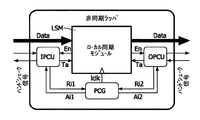
GALS構築ブロックの一般的なアーキテクチャが、図24に示されている。該アーキテクチャは、ローカル同期モジュールLSM(アイランド(island))の周囲の非同期ラッパ(wrapper)AWからなる。ラッパAWは、モジュールLSMの環境への通信を可能とし、同期モジュールLSM用のローカルなクロックを生成する。ネットワークオンチップNOCの環境において、ルータノードR及びネットワークインタフェースNI並びにIPブロック/クラスタは、斯かるラッピングされたモジュールAWにより実装される。クロックのローカルな生成は、環境との通信が進行中である場合又は要求される場合に、次のクロックサイクルを遅延させることを可能とする。ポートコントローラIPCU及びOPCUは、GALSシステム中のブロックの特定のポートにおける全てのデータ転送を管理するために備えられる。このことはモジュールLSMにより可能とされ、データ送信とローカルクロックの位相とを同期させるように働く。データを高速に且つ効率的に送信するため、ポートコントローラIPCU及びOPCUは、ローカルのクロック信号とは独立に動作する必要がある。このことは、これらコントローラを、非同期有限状態機械として実装することにより達成される。 The general architecture of the GALS building block is shown in FIG. The architecture consists of an asynchronous wrapper AW around the local synchronization module LSM (island). The wrapper AW enables communication to the environment of the module LSM and generates a local clock for the synchronization module LSM. In a network on chip NOC environment, the router node R and the network interface NI and the IP block / cluster are implemented by such a wrapped module AW. Local generation of the clock allows the next clock cycle to be delayed if communication with the environment is ongoing or required. Port controllers IPCU and OPCU are provided to manage all data transfers at specific ports of blocks in the GALS system. This is made possible by the module LSM and serves to synchronize the data transmission and the phase of the local clock. In order to transmit data at high speed and efficiently, the port controllers IPCU and OPCU need to operate independently of local clock signals. This is achieved by implementing these controllers as asynchronous finite state machines.
モジュール間通信についての多様な要求をカバーするため、ポートコントローラの2つのファミリ、即ちポール型ポート及びデマンド型ポートが有用である。ポール型(P型)ポートは、専ら準安定を防ぐためにクロック伸張のための要求を発行し、かくしてデータの正確さを確実にする。クロックは、可能な限り影響を受けない。デマンド型(D型)ポートもまた転送チャネル上でのデータの完全性を保証するが、クロックゲーティングに類似する特徴を加える。これがイネーブルとされるとすぐに、ローカルクロックを停止させ、要求された転送が起こるとすぐに解放する。 To cover the diverse requirements for inter-module communication, two families of port controllers are useful: poll type ports and demand type ports. A pole-type (P-type) port issues a request for clock expansion exclusively to prevent metastability, thus ensuring data accuracy. The clock is not affected as much as possible. Demand-type (D-type) ports also ensure data integrity on the transport channel, but add features similar to clock gating. As soon as this is enabled, the local clock is stopped and released as soon as the requested transfer occurs.
更に、入出力変形型におけるポート型の実装が図24に示されている。これらのポートコントローラは、2つのハンドシェーク対を持つ。一方はコントローラとクロック発生器との間にあり、他方はコントローラと対応するモジュールとの間にある。これらは、4位相ハンドシェーク(レベル信号)を利用する。更に、ポートイネーブルラインは、2位相プロトコル(遷移信号)を利用する。Taは、ポートコントローラからLSモジュールへの確認応答信号である。該信号のレベルは、データ語の転送が発生したか否かを示す。 Further, a port type implementation in the input / output variant is shown in FIG. These port controllers have two handshake pairs. One is between the controller and the clock generator, and the other is between the controller and the corresponding module. These utilize a 4-phase handshake (level signal). Further, the port enable line utilizes a two-phase protocol (transition signal). Ta is an acknowledgment signal from the port controller to the LS module. The level of the signal indicates whether or not a data word transfer has occurred.
図25において、図24の一時停止可能なクロック発生器のブロック図が示されている。一時停止可能なクロック発生器PCGは、GALSモジュールの重要な構成要素である。ここでは、テスト及びデバッグのための方法のない実装を示す。 In FIG. 25, a block diagram of the suspendable clock generator of FIG. 24 is shown. The pauseable clock generator PCG is an important component of the GALS module. Here we show an implementation without methods for testing and debugging.
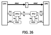
図26は、先行技術による、2つのローカルに同期したアイランド(LSM1、LSM2)の間の単一方向チャネルの実装を示す。上述したようなハンドシェークプロトコルが仮定される。ポートコントローラPCU間の接続は、ハンドシェーク信号Ap及びRpを介して確立される。ハンドシェーク確認応答信号Apにより制御されるデータラインdata1及びdata2上のラッチLは、通信モジュールLSM1及びLSM2を可能な限り分離する。転送チャネルにメモリを追加することは、受信側のクロックがデータを未だサンプリングしていなくても送信者が動作を再開することを可能とする。 FIG. 26 shows an implementation of a unidirectional channel between two locally synchronized islands (LSM1, LSM2) according to the prior art. A handshake protocol as described above is assumed. The connection between the port controller PCUs is established via handshake signals Ap and Rp. The latches L on the data lines data1 and data2 controlled by the handshake acknowledge signal Ap separate the communication modules LSM1 and LSM2 as much as possible. Adding memory to the transfer channel allows the sender to resume operation even if the receiving clock has not yet sampled the data.
図27は、D出力からP入力へのデータ転送の波形を示す。最初に、D出力がイネーブルにされ、自身のクロックを停止し、Rp+を発行する。このとき、受信ポートは未だイネーブルにされていない。このことが起こるとすぐに、該受信ポートがペンディング中のハンドシェークを検出し、自身のクロックを停止し、ハンドシェークに対して確認応答する。外部のハンドシェークが処理された後、両方のポート及び対応するモジュールLSMが、自身の動作を再開し得る。 FIG. 27 shows a waveform of data transfer from the D output to the P input. First, the D output is enabled, stops its own clock, and issues Rp +. At this time, the receiving port is not yet enabled. As soon as this happens, the receiving port detects a pending handshake, stops its clock, and acknowledges the handshake. After the external handshake is processed, both ports and the corresponding module LSM can resume their operation.
網掛けされたエリアは、データラッチLの透過位相(Ap=1)を示すものである。ラッチLが開いたとき受信クロックは非アクティブであり(Ai2=1)、その後ラッチの伝播遅延よりもかなり長い間非アクティブのままである。このことは、データライン上のイベントが受信側フリップフロップに安全に到達し、準安定が生じないことを確実にする。送信側クロックを停止したまま保つ(Ai1=1)ことは、ラッチが透過的である間data1が安定に保たれることを保証する。 The shaded area indicates the transmission phase (Ap = 1) of the data latch L. When latch L is opened, the receive clock is inactive (Ai2 = 1) and then remains inactive for much longer than the propagation delay of the latch. This ensures that events on the data line can safely reach the receiving flip-flop and metastability does not occur. Keeping the transmitting clock stopped (Ai1 = 1) ensures that data1 remains stable while the latch is transparent.
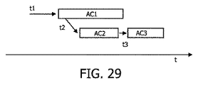
図28は、従来の非同期のシステムオンチップのブロック図を示す。3つの非同期回路AC1乃至AC3が示されている。非同期回路AC1乃至AC3のそれぞれは、自身の入力部の少なくとも1つにおいてデータが実際に存在するときにのみ起動される。従って、非同期回路AC1乃至AC3は時間の基準を持たないか、又は単にそれぞれの自身のローカルな時間の基準を持つ。 FIG. 28 shows a block diagram of a conventional asynchronous system-on-chip. Three asynchronous circuits AC1 to AC3 are shown. Each of the asynchronous circuits AC1 to AC3 is activated only when data is actually present in at least one of its own inputs. Thus, the asynchronous circuits AC1 to AC3 have no time reference or simply have their own local time reference.
図29は、3つの非同期回路AC1乃至AC3を持つ従来の非同期システムの実行追跡図を示す。ここで、非同期回路AC1乃至AC3は、時間の基準なく、個別にまた独立にトリガーされる。t1において、回路AC1用の入力が第1の回路AC1に到達する。t2において、第2の回路AC2用の入力が第1の回路AC1から到着する。t3において、第3の回路AC3用の入力が第2の回路AC2から到着する。 FIG. 29 shows an execution tracking diagram of a conventional asynchronous system having three asynchronous circuits AC1 to AC3. Here, the asynchronous circuits AC1 to AC3 are triggered individually and independently without a time reference. At t1, the input for the circuit AC1 reaches the first circuit AC1. At t2, the input for the second circuit AC2 arrives from the first circuit AC1. At t3, the input for the third circuit AC3 arrives from the second circuit AC2.
本発明の目的は、グローバルな同期クロックの非存在下でQoSを実装するための電子装置及び対応する方法を提供することにある。 It is an object of the present invention to provide an electronic device and corresponding method for implementing QoS in the absence of a global synchronous clock.
本目的は、請求項1による電子装置、請求項18による共有されたリソースを調停するための方法、及び請求項19による調停ユニット間で時間の基準を通信するためのトークンの使用により達成される。
This object is achieved by an electronic device according to
それ故、複数の第1の共有されたリソースと、それぞれが前記複数の第1の共有されたリソースの少なくとも1つについて調停を実行するための複数の調停ユニットと、を有する電子装置が提供される。前記調停ユニット間の通信は非同期に実行され、前記第1の共有されたリソース間のデータ通信は非同期に実行される。各前記調停ユニットは、第1のグローバルな時間の基準を実装するため、少なくとも1つの隣接する調停ユニットに第1のトークンを送信し、少なくとも1つの隣接する調停ユニットから第2のトークンを受信するように構成される。 Therefore, an electronic device is provided having a plurality of first shared resources and a plurality of arbitration units each for performing arbitration for at least one of the plurality of first shared resources. The Communication between the arbitration units is performed asynchronously, and data communication between the first shared resources is performed asynchronously. Each said arbitration unit transmits a first token to at least one adjacent arbitration unit and receives a second token from at least one adjacent arbitration unit to implement a first global time reference Configured as follows.
それ故、提案されるグローバルな調停方式は、調停ユニットの数においてスケーラブルであり、スケーラブルではない調停ユニット間の同期通信の使用に比して有利である。 Therefore, the proposed global arbitration scheme is scalable in the number of arbitration units and is advantageous over the use of synchronous communication between non-scalable arbitration units.
本発明の一態様によれば、前記電子装置は更に、複数のポートと、前記複数のポートを結合するための第1の共有されたリソースである非同期相互接続手段と、有する。前記相互接続手段は、それぞれが第2の共有されたリソースである複数の相互接続ユニットと、複数の調停ユニットと、を有し、前記複数の調停ユニットのそれぞれは、複数の前記第2の共有されたリソースの少なくとも1つについて調停を実行し、前記相互接続手段内の第2のグローバルな時間の基準を実装するため、少なくとも1つの隣接する相互接続構成要素へ第1のトークンを送信し、少なくとも1つの隣接する相互接続構成要素から第2のトークンを受信する。従って、非同期相互接続内で、及びそれ故ポート間で、QoSの実装を可能とする相互接続においてグローバルな時間の基準が実現される。 According to one aspect of the invention, the electronic device further comprises a plurality of ports and an asynchronous interconnect means that is a first shared resource for coupling the plurality of ports. The interconnection means includes a plurality of interconnection units, each of which is a second shared resource, and a plurality of arbitration units, each of the plurality of arbitration units being a plurality of the second shared resources. Sending a first token to at least one adjacent interconnect component to perform arbitration on at least one of the resources generated and implement a second global time reference in the interconnect means; A second token is received from at least one adjacent interconnect component. Thus, a global time reference is achieved in the interconnect that allows QoS implementation within the asynchronous interconnect and hence between ports.
本発明は更に、複数の共有されたリソースを持つ電子装置内で共有されたリソースを調停するための方法に関する。前記方法は、複数の第1の共有されたリソースの少なくとも1つについて、複数の調停が実行される。前記調停間の通信は、非同期に実行される。前記共有されたリソース間のデータ通信は、非同期に実行される。各前記調停するステップは、第1のグローバルな時間の基準を実装するため、少なくとも1つの隣接する調停に第1のトークンを送信するステップと、少なくとも1つの隣接する調停から第2のトークンを受信するステップと、を有する。 The invention further relates to a method for arbitrating a shared resource in an electronic device having a plurality of shared resources. The method performs a plurality of arbitrations for at least one of a plurality of first shared resources. Communication between the arbitrations is performed asynchronously. Data communication between the shared resources is executed asynchronously. Each said arbitrating step transmits a first token to at least one adjacent arbitration and receives a second token from at least one adjacent arbitration to implement a first global time reference. And a step of performing.
本発明は更に、電子装置における複数の第1の共有されたリソースの少なくとも1つについて複数の調停を実行するための調停ユニット間で時間の基準を通信するためのトークンの使用に関する。前記調停ユニット間の通信は、非同期に実行される。第1の共有されたリソース間のデータ通信は、非同期に実行される。このことは、トークンは通常単にデータを通信し、時間を通信しないため、有利である。 The invention further relates to the use of a token to communicate a time reference between arbitration units for performing a plurality of arbitrations for at least one of a plurality of first shared resources in an electronic device. Communication between the arbitration units is performed asynchronously. Data communication between the first shared resources is performed asynchronously. This is advantageous because tokens usually only communicate data and not time.
本発明は、分散されたグローバルな調停方式(例えばメモリコントローラ及びネットワークオンチップNOC調停方式、タイルベース方式における通信支援及びネットワークオンチップNOC調停方式)の非同期実装を提供するという発想に基づく。分散された態様において非同期で実装されることができる、グローバルな同期の基準(又は調停方式)が提供される。本発明はまた、レート制御された方式(例えば仮想回路キュー又は出力キュー)及びデッドラインベース方式のようなグローバルな同期の基準を必要とする他の調停方式を持つネットワークオンチップNOC(又はより一般的には、階層型/ブリッジされたバスのような通信基盤)に適用されることができる。根本的に、基本的な発想は、ネットワークオンチップNOCが、同期の論理的な単位(又は時間ステップ若しくはデータフロー射出)毎にトークンを交換する構成要素(例えばルータ、ネットワークインタフェース)から構成されることにより、グローバルな同期の基準(又はグローバルなスケジュール)を実装することができる点である。 The present invention is based on the idea of providing an asynchronous implementation of a distributed global arbitration scheme (eg memory controller and network on-chip NOC arbitration scheme, communication support in tile-based scheme and network on-chip NOC arbitration scheme). A global synchronization reference (or arbitration scheme) is provided that can be implemented asynchronously in a distributed manner. The present invention also provides network-on-chip NOC (or more general) with other arbitration schemes that require global synchronization criteria such as rate controlled schemes (eg virtual circuit queues or output queues) and deadline based schemes. In particular, it can be applied to a communication infrastructure such as a hierarchical / bridged bus). Fundamentally, the basic idea consists of components (e.g. routers, network interfaces) where the network-on-chip NOC exchanges tokens for every logical unit of synchronization (or time step or data flow injection). Thus, a global synchronization standard (or global schedule) can be implemented.
本発明は主に、(a)ネットワークオンチップNOCの同期レートの倍数又は約数でIPブロックを結合する非同期ネットワークオンチップNOC(即ち要求駆動型)、(b)ネットワークオンチップNOCの同期レートの倍数又は約数で動作しないIPブロックを結合する非同期ネットワークオンチップNOC(即ちデータ駆動型)、及び(c)ネットワークオンチップNOCの同期レートの倍数又は約数で動作しないIPブロックを結合する非同期ネットワークオンチップNOC(即ちイベント駆動型)、のケースに向けられたものである。 The present invention mainly includes (a) an asynchronous network-on-chip NOC (ie, request-driven type) that combines IP blocks at a multiple or a divisor of the network-on-chip NOC synchronization rate, Asynchronous network on-chip NOC that combines IP blocks that do not operate at multiples or divisors (ie, data driven), and (c) Asynchronous network that combines IP blocks that do not operate at multiples or divisors of network-on-chip NOC synchronization rates It is intended for the case of on-chip NOC (ie event driven).
本発明の更なる態様は、従属請求項に記載される。 Further aspects of the invention are set out in the dependent claims.
本発明のこれらの及び他の態様は、以下に説明される実施例を参照しながら、及び添付図面に関連して説明され明らかとなるであろう。 These and other aspects of the invention will be apparent from and elucidated with reference to the embodiments described hereinafter and in conjunction with the accompanying drawings.
QoS(とりわけ有限の待ち時間)を提供する本方法は、E. Rijpkema、K. Goossens及びP. Wielageによる「A router architecture for networks on silicon」(「2nd Workshop on Embedded Systems」、Proceedings of Progress 2001、オランダ国Veldhoven、2001年10月)に記載されたような、無衝突ルーティングの背景にあるデータフローモデルに存する。E. Rijpkema、K. G. W. Goossens、A. Radulescu、J. Dielissen、J. van Meerbergen、P. Wielage及びE. Waterlanderによる「Trade offs in the design of a router with both guaranteed and best-effort services for networks on chip」(「Automation and Test in Europe Conference and Exibition (DATE)、Proc. Design、350-355頁、2003年3月」により説明されているように、同期の論理単位はフリット(flit)であっても良い。本方式は、引用された論文において説明されているように、同期ベースで実装されても良いが、本発明により非同期実装のために実装されても良い。 This method of providing QoS (especially finite latency) is described by E. Rijpkema, K. Goossens and P. Wielage in “A router architecture for networks on silicon” (“2nd Workshop on Embedded Systems”, Proceedings of Progress 2001, Lies in the data flow model behind collision-free routing, as described in Veldhoven, October 2001). `` Trade offs in the design of a router with both guaranteed and best-effort services for networks on chip '' by E. Rijpkema, KGW Goossens, A. Radulescu, J. Dielissen, J. van Meerbergen, P. Wielage and E. Waterlander (As explained by "Automation and Test in Europe Conference and Exibition (DATE), Proc. Design, pp. 350-355, March 2003", the logical unit of synchronization may be a flit. This scheme may be implemented on a synchronous basis as described in the cited paper, but may also be implemented for asynchronous implementation according to the present invention.
図1は、本発明の第1の実施例による非同期システムのブロック図を示す。本システムは、幾つかの共有されたリソースSR1乃至SR4及び幾つかの調停ユニットAAU1乃至AAU4を有する。調停器間の通信、即ち調停器と調停器との間の通信は、非同期に実行される。共有されたリソースSR1乃至SR4は、これらリソース間でデータを通信しても良い。調停ユニットAAU1乃至AAU4のそれぞれは、自身の入力部にトークンTが存在するときに起動する。従って、非同期の調停器AAU1乃至AAU3は、グローバルで且つ共有された時間の基準を持つ。結果として、調停ユニットAAUは、該調停ユニットに関連する共有されたリソースを調停(断続線を参照)することができる。とりわけ、調停ユニットAAU1は共有されたリソースSR1に関連し、該共有されたリソースSR1を調停する。調停ユニットAAU2は共有されたリソースSR2に関連し、該共有されたリソースSR2を調停する。調停ユニットAAU3は共有されたリソースSR3及びSR5に関連し、該共有されたリソースSR3及びSR5を調停する。調停ユニットAAU4は共有されたリソースSR4に関連し、該共有されたリソースSR4を調停する。調停ユニットAAU1乃至AAU4の調停は、グローバルに同期された態様で、即ち協調した態様で実行される。共有されたリソースSR1乃至SR4は、これらリソース間でデータを通信しても良い。調停ユニットAAU1乃至AAU4は単に、グローバルな時間の基準を実装するため、隣接する調停ユニットと通信する。それ故、提案されるグローバルな調停方式は、調停ユニットの数においてスケーラブルであり、このことは、スケーラブルでない調停ユニット間の同期通信の使用に比して有利である。 FIG. 1 shows a block diagram of an asynchronous system according to a first embodiment of the present invention. The system has several shared resources SR1 to SR4 and several arbitration units AAU1 to AAU4. Communication between arbiters, that is, communication between the arbiter and the arbiter is performed asynchronously. Shared resources SR1 to SR4 may communicate data between these resources. Each of the arbitration units AAU1 to AAU4 is activated when the token T is present in its input unit. Thus, asynchronous arbiters AAU1 through AAU3 have a global and shared time reference. As a result, the arbitration unit AAU can arbitrate (see interrupted line) shared resources associated with the arbitration unit. In particular, the arbitration unit AAU1 is associated with the shared resource SR1 and arbitrates the shared resource SR1. The arbitration unit AAU2 is associated with the shared resource SR2, and arbitrates the shared resource SR2. The arbitration unit AAU3 is associated with the shared resources SR3 and SR5 and arbitrates the shared resources SR3 and SR5. The arbitration unit AAU4 is associated with the shared resource SR4 and arbitrates the shared resource SR4. The arbitration of the arbitration units AAU1 to AAU4 is performed in a globally synchronized manner, that is, in a coordinated manner. Shared resources SR1 to SR4 may communicate data between these resources. Arbitration units AAU1 through AAU4 simply communicate with neighboring arbitration units to implement a global time reference. The proposed global arbitration scheme is therefore scalable in the number of arbitration units, which is advantageous compared to the use of synchronous communication between non-scalable arbitration units.
グローバルな時間の基準とは、(ことによると全ての)調停ユニットが、(全ての)他の調停ユニットの状況又は状態を知っている状況を示す。それ故、或る調停ユニットがステップ3にある場合、他の全ての調停ユニットもステップ3にあることとなる。
A global time reference refers to a situation where (possibly all) arbitration units know the status or status of (all) other arbitration units. Therefore, if a mediation unit is in
図2(a)及び2(b)は、第1の実施例による幾つかのIPブロックを結合するマルチホップ相互接続IMのブロック図を示す。相互接続IMは、幾つかのルータRと、該ルータをIPブロックIPに接続させるための相互接続構成要素又は相互接続ノードとしてのネットワークインタフェースNIとを有する。 2 (a) and 2 (b) show block diagrams of a multi-hop interconnect IM that combines several IP blocks according to the first embodiment. The interconnection IM has several routers R and a network interface NI as an interconnection component or interconnection node for connecting the routers to the IP block IP.
ルータR(又は他のネットワークオンチップNOCの構成要素)の非同期の実装は、起動/リセット時に、最初に、全ての出力部、即ち図2aに示されたような他のネットワークオンチップNOC構成要素への各リンクにおけるトークンTの生成に帰着し、次いで(永久に又はリセットまで)全ての入力部からトークンを読み出し、図2bに示されるようにトークンを処理し、全ての出力部においてトークンTを生成する。このようにして、全てのルータが、例えば同一のTDMAスロットにおいて、横並びで進行する。このことは、ローカルである傾向がある隣接するものへの非同期のハンドシェークのみを用いたグローバルな調停方式を実装する効果を持つ。トークンを生成し消費することは、要求駆動(要求−確認応答)型のインタラクション(ハンドシェーク)に対応する。 Asynchronous implementation of router R (or other network-on-chip NOC components) first starts up / reset, all outputs, ie other network-on-chip NOC components as shown in FIG. 2a. Resulting in the generation of token T at each link to, then reading the token from all inputs (permanently or until reset), processing the token as shown in FIG. Generate. In this way, all routers proceed side by side, for example in the same TDMA slot. This has the effect of implementing a global arbitration scheme that uses only asynchronous handshaking to neighbors that tend to be local. Generating and consuming tokens corresponds to a request-driven (request-acknowledgement) type interaction (handshake).
この概念は、レート制御された及びデッドラインベースのグローバルな調停方式にも利用されることができる。トークンTは、データを含むか、又は空であることに留意されたい。データがない場合であっても、これらトークンは同期の基準を維持するために送信される必要がある。 This concept can also be utilized for rate controlled and deadline based global arbitration schemes. Note that the token T contains data or is empty. Even in the absence of data, these tokens need to be sent to maintain synchronization criteria.
非同期相互接続IMのためのQoSの実装が、ここで説明される。ネットワークオンチップNOC構成要素は、最も低速な構成要素と同じように低速に進み、全体としてネットワークオンチップNOCの同期レートを構成する。1秒ごとの繰り返しの回数は、「実クロック速度」に関連する。例えば、同期ステップは3個のクロックサイクルに対応しても良い。同期レートがネットワークオンチップNOCにおいて内部的に、即ち最も低速な構成要素によって生成され、(完全に同期的なネットワークオンチップNOCにおけるように)外部の既知のクロックにより課せられるものではないという事実は、問題となるものではなく、QoSの概念を無効化するものではない。なぜなら、該ネットワーク内の全ての非同期の構成要素が、考慮される動作の特定の目標周波数で設計されるからである。 A QoS implementation for the asynchronous interconnect IM will now be described. The network-on-chip NOC component goes to the low speed in the same way as the slowest component and constitutes the network-on-chip NOC synchronization rate as a whole. The number of repetitions per second is related to the “real clock speed”. For example, the synchronization step may correspond to 3 clock cycles. The fact that the synchronization rate is generated internally in the network-on-chip NOC, ie by the slowest component, and not imposed by an external known clock (as in a fully synchronous network-on-chip NOC) This is not a problem and does not invalidate the QoS concept. This is because all asynchronous components in the network are designed with a specific target frequency of operation to be considered.
説明のための例として、目標周波数は、166M同期/秒、即ち166メガフリット/秒であっても良い。ここでフリットとは、それぞれが32ビットの3個のワードであっても良い。例えば20%のような適切なマージンをとる(即ち「オーバ・デザイニング」)ことにより、構成要素は200M同期/秒即ち200Mフリット/秒で動作するが、最も低速な構成要素は意図された166M同期/秒即ち500Mワード/秒よりも確実に高速に動作し、少なくとも166M同期/秒即ち500Mワード/秒の保証されたスループットに導き、潜在的により高速に動作するネットワークオンチップNOCに導く。実際のマージンは、チップの処理の正確さ、ワーストケースの動作条件等に依存するものとなるであろう。この論法は同期及び非同期のモジュール/ICについて等しく受け入れられる。 As an illustrative example, the target frequency may be 166M sync / sec, or 166 megafrit / sec. Here, the flit may be three words each having 32 bits. By taking an appropriate margin, eg 20% (ie “over-designing”), the component will operate at 200M sync / second or 200M flits / sec, while the slowest component will be the intended 166M sync It operates reliably and faster than 500M words / second, leading to a guaranteed throughput of at least 166M sync / second or 500M words / second, leading to a potentially faster operating network-on-chip NOC. The actual margin will depend on the accuracy of the chip processing, the worst case operating conditions, and the like. This reasoning is equally acceptable for synchronous and asynchronous modules / ICs.
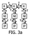
図3乃至dは、第2の実施例による、ルータR及び、相互接続としてのネットワークインタフェースNI、並びにそれぞれのネットワークインタフェースNIに結合されたIPブロックIPを持つネットワークオンチップを示す。IPブロックは、種々のトークンレートを利用して、倍数のレート(又は約数のレート)で動作し得る。従って、ネットワークオンチップNOCの同期レートの倍数又は約数で動作するIPブロックIPとの非同期マルチホップ相互接続IMのQoSが示されている。図3aにおいて、IPブロックIPは相互接続の倍のレートで動作し、それ故、ルータR及びネットワークインタフェースNIが単に単一のトークンTを生成する間に、2つの動作トークンTを生成する。 FIGS. 3 to d show a network-on-chip having a router R and a network interface NI as an interconnection and an IP block IP coupled to each network interface NI according to the second embodiment. An IP block may operate at multiple rates (or divisor rates) utilizing various token rates. Thus, the QoS of an asynchronous multi-hop interconnect IM with an IP block IP operating at multiples or divisors of the network-on-chip NOC synchronization rate is shown. In FIG. 3a, the IP block IP operates at twice the rate of interconnection, so it generates two operational tokens T while the router R and the network interface NI simply generate a single token T.
両方のケースにおいて、本方法は、ネットワークオンチップNOCの周波数の倍数又は約数で動作するIPブロックにのみ適用可能である。更に、同期の場合には、ネットワークオンチップNOCに接続された全てのIPブロックのために動作する単一の同期クロックを持つことはもはや実現可能ではない。 In both cases, the method is only applicable to IP blocks that operate at multiples or divisors of the network-on-chip NOC frequency. Furthermore, in the case of synchronization, it is no longer feasible to have a single synchronization clock that operates for all IP blocks connected to the network on chip NOC.
同期の場合には、IP及びネットワークオンチップNOC(1つのクロックで動作する)のための複数の独立したクロックの使用は、データの同期、即ち或る(IPの)クロックドメインから他のもの(ネットワークオンチップNOCのもの)への交差又はその逆のための直列の2つのフリップフロップの利用に依存する。このことは、データ駆動型同期と呼ばれる。斯かる方法は動作するが最適ではない。なぜなら、他のクロックドメインからサンプリングデータが来たときにエラーが発生し得るからである。該状態は、両方の周波数が増大するにつれて更に悪化する。 In the case of synchronization, the use of multiple independent clocks for IP and network-on-chip NOCs (running with one clock) is the synchronization of data, ie from one (IP) clock domain to another ( Depends on the use of two flip-flops in series for crossing to the network on-chip NOC) and vice versa. This is called data driven synchronization. Such a method works but is not optimal. This is because an error may occur when sampling data comes from another clock domain. The condition gets worse as both frequencies increase.
非同期の場合には、同期の論理的な基準により動作するIP及びネットワークオンチップNOCのための複数の独立したクロックの同期は、要求駆動型同期、データ同期又はイベント駆動型同期により解決されることができる。第1の方法は、全てのクロック比、可変クロック等に対処することはできない。第2の方法は、不正確なデータの可能性を導く。第3の方法は、どちらの問題も持たない。 In the case of asynchronous, synchronization of multiple independent clocks for IP and network-on-chip NOCs operating on the logical basis of synchronization should be resolved by request driven synchronization, data synchronization or event driven synchronization Can do. The first method cannot cope with all clock ratios, variable clocks, and the like. The second method introduces the possibility of inaccurate data. The third method does not have either problem.
データ駆動型の同期の場合においては、他のモジュールへの通信ラインの全てにおける全てのモジュールが、クロックを進めるときにラインをサンプリングする。このことは、二重フリップフロップ方式により為され得る。不正確なデータサンプルという潜在的な問題が導かれる。とりわけ、2つのフリップフロップを利用してサンプリングされたビットが不正確である可能性がある。より多くのフリップフロップを利用することにより、増大される待ち時間と引き換えに、この可能性は低減させられる。ここで、本システム上の全てのデータ駆動型ポート/リンクについて該エラーの可能性が存在し、エラーが互いを相殺しない即ち互いを補償しないという意味で、これらの可能性が合算されることに留意されたい。 In the case of data driven synchronization, all modules in all of the communication lines to other modules sample the line as they advance the clock. This can be done by a double flip-flop scheme. A potential problem of inaccurate data samples is introduced. In particular, bits sampled using two flip-flops can be inaccurate. By utilizing more flip-flops, this possibility is reduced at the expense of increased latency. Here, the possibility of the error exists for all data-driven ports / links on the system, and these possibilities are summed in the sense that the errors do not cancel each other, ie do not compensate each other. Please keep in mind.
要求駆動型の同期が図2及び図3に示され、ネットワークオンチップNOCモジュール(NI及びルータ)間の実施例を構成する。送信されるデータにおいてエラーは発生しない。 Request-driven synchronization is illustrated in FIGS. 2 and 3 and constitutes an embodiment between network on-chip NOC modules (NI and router). No error occurs in the transmitted data.
図4は、第2の実施例による、3つのIPブロックIPを結合するためのネットワークオンチップNOCのブロック図を示す。該ネットワークオンチップは、3つのルータRと共に、3つのネットワークインタフェースNIを有する。ルータR及びネットワークインタフェースNIは、D型ポートDを介して通信する。 FIG. 4 shows a block diagram of a network on chip NOC for combining three IP blocks IP according to the second embodiment. The network on chip has three network interfaces NI together with three routers R. The router R and the network interface NI communicate via a D-type port D.
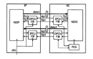
図5は、IPブロックIP、ネットワークインタフェースNI及びルータRのブロック図を示す。IPブロックIPとネットワークインタフェースNIとの間のインタフェースは適切なクロック方式に基づいて実装され、ネットワークインタフェースNIとルータRとの間のインタフェースは要求駆動型の同期に基づいて実装される。IPブロックIPからネットワークインタフェースNIへの通信は、IPブロックからの要求信号ip2ni_valid、及びネットワークインタフェースからの応答信号ip2ni_ack、並びに要求データreqdataにより実装される。ネットワークインタフェースNIからIPブロックIPへの通信は、ネットワークインタフェースNIからの要求信号ni2ip_valid、及びIPブロックIPからの応答信号ni2ip_ack、並びに応答データrespdataにより実装される。更に、ネットワークインタフェースNIからルータRへの通信は、ネットワークインタフェースNIからの要求信号ni2r_valid、及びルータRからの応答信号r2ni_ack、並びにni2r_dataにより実装される。ルータRからネットワークインタフェースNIへの通信は、ルータからの要求信号r2ni_valid、及びネットワークインタフェースからの応答信号r2ni_ack、並びにデータr2ni_dataにより実装される。 FIG. 5 shows a block diagram of the IP block IP, the network interface NI, and the router R. The interface between the IP block IP and the network interface NI is implemented based on an appropriate clock system, and the interface between the network interface NI and the router R is implemented based on request-driven synchronization. Communication from the IP block IP to the network interface NI is implemented by a request signal ip2ni_valid from the IP block, a response signal ip2ni_ack from the network interface, and request data reqdata. Communication from the network interface NI to the IP block IP is implemented by a request signal ni2ip_valid from the network interface NI, a response signal ni2ip_ack from the IP block IP, and response data respdata. Further, communication from the network interface NI to the router R is implemented by a request signal ni2r_valid from the network interface NI, a response signal r2ni_ack from the router R, and ni2r_data. Communication from the router R to the network interface NI is implemented by a request signal r2ni_valid from the router, a response signal r2ni_ack from the network interface, and data r2ni_data.
ネットワークインタフェースNIは、相互排斥ユニットmutexに接続された排他的ORユニットXORを有し、該相互排斥ユニットmutexはトグルユニットTUに接続されている。トグルユニットTUの出力部は論理ユニットLUに接続され、応答信号ip2ni_ackを構成する。遅延ライン及びインバータDLIを持つフィードバックループは、相互排斥ユニットmutexに結合されている。2入力相互排斥要素mutexは、標準的な非同期構築ブロックである。 The network interface NI has an exclusive OR unit XOR connected to the mutual exclusion unit mutex, which is connected to the toggle unit TU. The output unit of the toggle unit TU is connected to the logical unit LU and constitutes a response signal ip2ni_ack. A feedback loop having a delay line and an inverter DLI is coupled to the mutual rejection unit mutex. The two-input mutual exclusion element mutex is a standard asynchronous building block.
ネットワークインタフェースNIの応答部は、遅延及びインバータDLIのない対応する態様で構成される。 The response part of the network interface NI is configured in a corresponding manner without delay and inverter DLI.
基本的に、IPからの外部イベントがNIに到達したときにはいつでも、状態要素が該情報(IPが通信したもの)を保存するためにトグルされ、それにより該情報が論理ブロックにより利用されることができる。該イベントは次いで、IPブロックIPへの信号ip2ni_ackにより確認応答される。IPブロックに対する確認応答はクリティカルパス上にあり、可能な限り迅速である必要がある。この理由のため、トグル要素TUは、潜在的に非常に低速なIPブロックからのいずれのインタラクションをも必要とすることなく、即座に、(相互排斥要素へと向かう)要求ラインをローにする。IPブロックは次いで、都合の良いときに確認応答に応答する。論理ユニットLUは、例えば要求データを読み出すために、要求ラインip2ni_validがハイであるという情報を利用する。 Basically, whenever an external event from IP reaches NI, the state element is toggled to store the information (what the IP communicated with), so that the information is used by the logic block. it can. The event is then acknowledged by a signal ip2ni_ack to the IP block IP. Acknowledgments for IP blocks are on the critical path and need to be as quick as possible. For this reason, the toggle element TU immediately pulls the request line (toward the mutual exclusion element) low without requiring any interaction from a potentially very slow IP block. The IP block then responds with an acknowledgment when convenient. The logical unit LU uses information that the request line ip2ni_valid is high in order to read out the request data, for example.
図6は、図5によるIPブロックIP、ネットワークインタフェースNI及びルータRのブロック図を示す。しかしながら、図6によれば、同期NIコアNSNIが再利用されても良い。図6の他の構成は、図5の構成に対応する。換言すれば、非同期のネットワークインタフェースが実装されるべき場合には、このことは同期ネットワークインタフェースの典型的な構造を利用することにより達成され、斯かる典型的な構造の上端においてIPブロックIPへの通信を可能とするための一種の内部シェルを提供する。 FIG. 6 shows a block diagram of the IP block IP, network interface NI and router R according to FIG. However, according to FIG. 6, the synchronous NI core NSNI may be reused. The other configuration in FIG. 6 corresponds to the configuration in FIG. In other words, if an asynchronous network interface is to be implemented, this is achieved by utilizing the typical structure of a synchronous network interface and at the top of such a typical structure to the IP block IP. Provide a kind of internal shell to enable communication.
上述の動作は通常、NIの内部的に生成されたクロックを全く停止させないことは留意されるべきである。 It should be noted that the above operations typically do not stop the NI's internally generated clock at all.
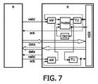
図7は、図4の2つの隣接するルータのより詳細なブロック図を示す。ルータR間のインタフェースは、要求駆動型の同期に基づいて実装される。ルータ間の通信は、要求信号valid及び応答信号ack並びに要求データdataにより実装される。 FIG. 7 shows a more detailed block diagram of the two adjacent routers of FIG. The interface between routers R is implemented based on request driven synchronization. Communication between routers is implemented by a request signal valid, a response signal ack, and request data data.
前記ルータは相互排斥ユニットmutexに接続された排他的ORユニットXORを有し、該相互排斥ユニットmutexはトグルユニットTUに接続されている。トグルユニットTUの出力部は、同期ルータコアNSRに接続されている。遅延ライン及びインバータDLIを持つフィードバックループは、相互排斥ユニットmutexに結合されている。2入力相互排斥要素mutexは、標準的な非同期構築ブロックである。 The router has an exclusive OR unit XOR connected to a mutual exclusion unit mutex, which is connected to a toggle unit TU. The output unit of the toggle unit TU is connected to the synchronous router core NSR. A feedback loop having a delay line and an inverter DLI is coupled to the mutual rejection unit mutex. The two-input mutual exclusion element mutex is a standard asynchronous building block.
図8は、図4の2つの隣接するルータの更に詳細なブロック図を示す。該ルータは、通常の同期ルータコアNSR及び一時停止可能なクロック発生器PCGを有する。 FIG. 8 shows a more detailed block diagram of the two adjacent routers of FIG. The router has a normal synchronous router core NSR and a clock generator PCG that can be paused.
図9は、第2の実施例による図4のルータRのブロック図を示す。ルータRは、ルータRを隣接するルータR、及びことによると隣接するネットワークインタフェースNIへと結合させる、要求駆動型のインタフェースを有するであろう。ルータRは、入力ポート制御ユニットIPCU及び出力ポート制御ユニットOPCUを持つコアとして、通常の同期ルータNSRを有する。入力ポート制御ユニットIPCU及び出力ポート制御ユニットOPCUは、D型ポートとして実装される。2つのポート制御ユニットIPCU及びOPCUは、一時停止可能なクロック発生器PCGに結合される。ルータRと隣接するルータとの間の通信は、ルータRの入力側においてハンドシェーク信号AP1及びRP1を介して実行され、ルータは入力データdata1を受信する。ルータRの出力側においては、隣接するルータRへの通信はハンドシェーク信号AP2及びRP2を介して実行され、data2が後続するルータへと転送される。 FIG. 9 shows a block diagram of the router R of FIG. 4 according to the second embodiment. Router R will have a request driven interface that couples router R to an adjacent router R and possibly to an adjacent network interface NI. The router R has a normal synchronous router NSR as a core having an input port control unit IPCU and an output port control unit OPCU. The input port control unit IPCU and the output port control unit OPCU are implemented as D-type ports. The two port control units IPCU and OPCU are coupled to a suspendable clock generator PCG. Communication between the router R and the adjacent router is performed on the input side of the router R via the handshake signals AP1 and RP1, and the router receives the input data data1. On the output side of the router R, communication to the adjacent router R is executed via the handshake signals AP2 and RP2, and data2 is transferred to the subsequent router.
図10の上部において、ネットワークオンチップの一部のブロック図が示される。図10は、第2の実施例によるネットワークオンチップの一部を示す。ここで、マスタIPブロックMIP(マスタとして動作する)、マスタネットワークインタフェースmNI、1以上のルータR、スレーブネットワークインタフェース、及びスレーブIPブロックSIP(スレーブとして動作する)が示されている。これらのユニットは、論理的に同期した、即ち同一のクロックドメイン中にある又は固定されたレートで同期している、リンクL1、L2、L3及びL4により接続される。換言すれば、IPブロックMIP及びSIP並びに相互接続mNI、R及びsNIは、論理的に同期している。いずれの時間に関連するQoSも、マスタIPブロックMIPからスレーブIPブロックSIPへと達することができる。 In the upper part of FIG. 10, a block diagram of a part of the network on chip is shown. FIG. 10 shows a part of the network on chip according to the second embodiment. Here, a master IP block MIP (operating as a master), a master network interface mNI, one or more routers R, a slave network interface, and a slave IP block SIP (operating as a slave) are shown. These units are connected by links L1, L2, L3 and L4 which are logically synchronized, ie in the same clock domain or synchronized at a fixed rate. In other words, the IP blocks MIP and SIP and the interconnections mNI, R and sNI are logically synchronized. Any time-related QoS can reach from the master IP block MIP to the slave IP block SIP.
図10は、該図の下部において、ネットワークオンチップの同一の部分を示すが、ここでは相互接続IM、マスタネットワークインタフェースmNI、ルータR及びスレーブネットワークインタフェースsNIのみが論理的に同期している。いずれの時間に関連するQoSもが、マスタネットワークインタフェースmNIからスレーブネットワークインタフェースsNIへと達する。即ち、リンクL1とL4とが同期していないため、マスタIPブロックMIPからスレーブIPブロックSIPまでは達しない。データ駆動型同期を可能とするためにこれらリンクL1及びL4を通る通信のためのデータがサンプリングされる必要があるか、又はイベント駆動型同期を可能とするためにそれぞれのクロックが同期される必要がある。 FIG. 10 shows the same part of the network on chip in the lower part of the figure, but here only the interconnect IM, master network interface mNI, router R and slave network interface sNI are logically synchronized. The QoS associated with any time reaches from the master network interface mNI to the slave network interface sNI. That is, since the links L1 and L4 are not synchronized, the master IP block MIP does not reach the slave IP block SIP. Data for communication over these links L1 and L4 needs to be sampled to enable data driven synchronization or the respective clocks need to be synchronized to enable event driven synchronization There is.
ここで、ネットワークオンチップNOC(同期又は非同期)とIPブロックとの間のインタラクションが考慮される。ネットワークオンチップNOCにより実装されるようなQoS(例えば保証された待ち時間)は、マスタmNIからスレーブmNIまでのみ亘る。マスタ(又はスレーブ)及びネットワークオンチップNOC(即ち(マスタ(又はスレーブ)NI)が同期して動作する場合、即ち同一の又は導出されたクロックドメインにある場合(即ちクロックドメインの交差がない場合)、QoSの保証はマスタからスレーブまで達する。同様に、ネットワークオンチップNOCが非同期である場合、マスタ(又はスレーブ)は全ての(固定された倍数)時間ステップをマスタ(又はスレーブ)NIと同期させ、QoSはマスタMIPからスレーブSIPへと達する。従って、このことは非同期(マルチレートSDF)状態、即ち要求駆動型同期に対応することとなる。 Here, the interaction between the network on chip NOC (synchronous or asynchronous) and the IP block is considered. The QoS (eg, guaranteed latency) as implemented by the network on chip NOC extends only from the master mNI to the slave mNI. When the master (or slave) and the network on chip NOC (ie (master (or slave) NI) operate synchronously, ie in the same or derived clock domain (ie there is no clock domain crossing)) QoS guarantees reach from master to slave Similarly, if the network-on-chip NOC is asynchronous, the master (or slave) synchronizes all (fixed multiple) time steps with the master (or slave) NI. , QoS reaches from the master MIP to the slave SIP, so this corresponds to an asynchronous (multi-rate SDF) state, ie request driven synchronization.
図11において、第3の実施例によるネットワークオンチップの一部のブロック図が示される。単に本発明を説明するため、1つのIPブロックIP、1つのネットワークインタフェースNI、及び単に1つのルータRが示されている。IPブロックIPとネットワークインタフェースとの間の通信は、IPブロックIP及びネットワークインタフェースNIにおけるD型ポートDを用いてD型インタフェースを介して実行される。ネットワークインタフェースNIと関連するルータRとの間の通信もまた、D型ポートDを用いてD型インタフェースに基づいて実行される。このことは、ルータ間通信にも当てはまる。従って、ネットワークオンチップNOCとIPブロックIPとの間の要求駆動型通信が示される。ここでIPブロックは、ネットワークオンチップのレートと同一または倍数若しくは約数のレートで処理を実行する。 FIG. 11 shows a block diagram of a part of the network on chip according to the third embodiment. Only one IP block IP, one network interface NI, and only one router R are shown for illustrative purposes only. Communication between the IP block IP and the network interface is performed via the D-type interface using the D-type port D in the IP block IP and the network interface NI. Communication between the network interface NI and the associated router R is also performed based on the D interface using the D port D. This is also true for inter-router communication. Thus, request driven communication between the network on chip NOC and the IP block IP is shown. Here, the IP block executes processing at the same rate, a multiple or a divisor rate as the network on-chip rate.
図12において、IPブロックIP及びネットワークインタフェースNIのより詳細なブロック図が示される。IPブロックIPは、通常の同期IPコアNSIPを有する。入力ポート制御ユニットIPCU及び出力ポート制御ユニットOPCUは、通常同期IPユニットNSIPに結合されている。これらユニットは共に、D型ポートとして実装される。これらポート制御ユニットは、一時停止可能なクロック発生器PCGに結合される。ネットワークインタフェースNIは、入力ポート制御ユニットIPCU及び出力ポート制御ユニットOPCUを伴う、通常同期ネットワークインタフェースコアNSNIを有する。これらポート制御ユニットは共に、一時停止可能なクロック発生器PCGに結合される。IPブロックからネットワークインタフェースNIへの通信はハンドシェーク信号AP1及びRP1を介して処理され、データdata1がIPブロックIPからネットワークインタフェースNIへと転送される。ネットワークインタフェースからIPブロックへの通信は第2のハンドシェーク信号AP2及びRP2を介して処理され、データdata2がネットワークインタフェースNIからIPブロックIPへと転送される。従って、要求駆動型インタフェースが、IPブロックIPとネットワークインタフェースNIとの間に実装される。 In FIG. 12, a more detailed block diagram of the IP block IP and the network interface NI is shown. The IP block IP has a normal synchronous IP core NSIP. The input port control unit IPCU and the output port control unit OPCU are coupled to the normal synchronous IP unit NSIP. Both units are implemented as D-type ports. These port control units are coupled to a suspendable clock generator PCG. The network interface NI has a normal synchronous network interface core NSNI with an input port control unit IPCU and an output port control unit OPCU. Both of these port control units are coupled to a suspendable clock generator PCG. Communication from the IP block to the network interface NI is processed via the handshake signals AP1 and RP1, and the data data1 is transferred from the IP block IP to the network interface NI. Communication from the network interface to the IP block is processed via the second handshake signals AP2 and RP2, and the data data2 is transferred from the network interface NI to the IP block IP. Therefore, a request driven interface is implemented between the IP block IP and the network interface NI.
図13は、図11のネットワークインタフェースのより詳細なブロック図を示す。該ネットワークインタフェースは、D型ポートとして実装されるルータ及びIPの両方に対する要求駆動型インタフェースを有する。 FIG. 13 shows a more detailed block diagram of the network interface of FIG. The network interface has a request driven interface for both routers and IP implemented as D-type ports.
図14は、第4の実施例によるネットワークオンチップのブロック図部分を示す。該ネットワークオンチップの基本構造は、図11による構造に対応する。しかしながら、IPブロックIPとネットワークインタフェースNIとの間のインタフェースは、P型インタフェースである。それ故、IPブロックは2つのP型ポートを有し、ネットワークインタフェースNIもまた2つのP型ポートを有する。ネットワークインタフェースとルータとの間の通信及びルータ間通信は、D型ルータを用いたD型インタフェースに基づく。 FIG. 14 shows a block diagram portion of a network-on-chip according to the fourth embodiment. The basic structure of the network on chip corresponds to the structure according to FIG. However, the interface between the IP block IP and the network interface NI is a P-type interface. Therefore, the IP block has two P-type ports and the network interface NI also has two P-type ports. Communication between a network interface and a router and communication between routers are based on a D-type interface using a D-type router.
図15は、第4の実施例による図14によるIPブロックIP及びネットワークインタフェースのより詳細なブロック図を示す。図15のIPブロック及びネットワークインタフェースの基本構造は、図12によるネットワークインタフェース及びIPブロックの構造に対応する。しかしながら、P型ポート制御ユニットとしてポート制御ユニットOPCU及びIPCUが実装され、これによりP型インタフェースがIPブロックとネットワークインタフェースとの間に実装される。従って、IPブロックIPとネットワークインタフェースNIとの間にイベント駆動型インタフェースが実装される。IPブロックからネットワークインタフェースへの通信は第1のハンドシェーク信号AP1及びRP1並びにdata1を介して制御され、ネットワークインタフェースからIPブロックへの通信は第2のハンドシェーク信号AP2及びRP2並びにネットワークインタフェースNIからIPブロックIPへ転送されるdata2を介して制御される。 FIG. 15 shows a more detailed block diagram of the IP block IP and network interface according to FIG. 14 according to the fourth embodiment. The basic structure of the IP block and the network interface in FIG. 15 corresponds to the structure of the network interface and the IP block according to FIG. However, port control units OPCU and IPCU are mounted as P-type port control units, and thereby the P-type interface is mounted between the IP block and the network interface. Accordingly, an event driven interface is implemented between the IP block IP and the network interface NI. Communication from the IP block to the network interface is controlled via the first handshake signals AP1 and RP1 and data1, and communication from the network interface to the IP block is from the second handshake signals AP2 and RP2 and the network interface NI to the IP block IP. Controlled via data2 transferred to.
図16は、図14のネットワークインタフェースのより詳細なブロック図を示す。ネットワークインタフェースは、それぞれがP型ポート及びD型ポートとして実装された、1つのイベント駆動型インタフェース(IPへの通信用)及び要求駆動型インタフェース(ルータへの通信用)を有する。 FIG. 16 shows a more detailed block diagram of the network interface of FIG. The network interface has one event-driven interface (for communication to IP) and request-driven interface (for communication to router), each implemented as a P-type port and a D-type port.
図17は、第5の実施例によるIPブロックに結合されたネットワークオンチップの一部のブロック図を示す。該ネットワークオンチップ及びIPブロックの構造は、図11及び図14の構造に対応する。ネットワークインタフェースNIとルータとの間の通信及びルータ間通信は、D型ポートを用いたD型インタフェースに基づく。しかしながら、IPブロックとネットワークインタフェースとの間の通信はデータ駆動型インタフェースを用いて実行され、IPブロックはS型ポートを有し、ネットワークインタフェースはP型ポートを有する。ここで、IPブロックはネットワークオンチップのレートとは独立したレートで動作しても良い。 FIG. 17 shows a block diagram of a part of a network on chip coupled to an IP block according to a fifth embodiment. The structure of the network-on-chip and the IP block corresponds to the structure of FIGS. Communication between the network interface NI and the router and communication between routers are based on a D-type interface using a D-type port. However, communication between the IP block and the network interface is performed using a data driven interface, the IP block has an S-type port, and the network interface has a P-type port. Here, the IP block may operate at a rate independent of the network-on-chip rate.
図18は、図17のIPブロックIP及びネットワークインタフェースNIのより詳細なブロック図を示す。図18のIPブロック及びネットワークインタフェースの基本構造は、図12及び図16の基本構造に対応する。しかしながら、IPブロックはS型ポート制御ユニットOPCU及びIPCUを有し、ネットワークインタフェースはP型ポート制御ユニットIPCU及びOPCUを有する。 18 shows a more detailed block diagram of the IP block IP and network interface NI of FIG. The basic structure of the IP block and network interface in FIG. 18 corresponds to the basic structure in FIGS. However, the IP block has S-type port control units OPCU and IPCU, and the network interface has P-type port control units IPCU and OPCU.
図19は、図17のネットワークインタフェースのより詳細なブロック図を示す。該ネットワークインタフェースは、それぞれがS型ポート及びP型ポートとして実装された、1つの要求駆動型インタフェース及び要求駆動型インタフェースを有する。 FIG. 19 shows a more detailed block diagram of the network interface of FIG. The network interface has one request driven interface and a request driven interface, each implemented as an S-type port and a P-type port.
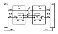
図20は、第7の実施例による、2つのローカルに同期したアイランド(LSM1、LSM2)間の単一方向チャネルの実装のブロック図を示す。出力ポート制御ユニットOPCUと入力ポート制御ユニットIPCUとの間の接続は、ハンドシェーク信号Ap及びRpを介して確立される。ハンドシェーク確認応答信号Apにより制御されるデータラインdata1及びdata2上のラッチLは、通信モジュールLSM1とLSM2とを可能な限り分離する。 FIG. 20 shows a block diagram of an implementation of a unidirectional channel between two locally synchronized islands (LSM1, LSM2) according to a seventh embodiment. The connection between the output port control unit OPCU and the input port control unit IPCU is established via handshake signals Ap and Rp. The latches L on the data lines data1 and data2 controlled by the handshake confirmation response signal Ap separate the communication modules LSM1 and LSM2 as much as possible.
ここで、停止されることができないクロックで動作するローカルに同期したアイランドLSM1及びLSM2用の出力及び入力ポートコントローラOPCU及びIPCUのために、S型ポートが利用される。斯かるクロックは一般に、外部的に生成されたクロックである。斯かるローカルに同期したアイランドLSM1及びLSM2は、一時停止可能なクロック発生器PCGを持たない。ローカルに同期したアイランドLSM1及びLSM2は、(En信号をトグルすることにより)S型ポートがデータ通信を実行することを可能とすることができる。信号Taがトグルするとき、データ通信が実行されている。S型ポートはいずれのクロックとも干渉しないため、S型ポートの実装は基本的に、自由に動作するP型ポートである。信号TaをLSMクロック信号と同期させるため、フリップフロップFFが利用される。それ故、P及びD型ポートにより利用されるクロック同期の代わりに、データ同期が利用される。 Here, S-type ports are used for the output and input port controllers OPCU and IPCU for the locally synchronized islands LSM1 and LSM2 operating with a clock that cannot be stopped. Such a clock is generally an externally generated clock. Such locally synchronized islands LSM1 and LSM2 do not have a suspendable clock generator PCG. Locally synchronized islands LSM1 and LSM2 can enable the S-type port to perform data communication (by toggling the En signal). Data communication is being performed when the signal Ta toggles. Since the S-type port does not interfere with any clock, the implementation of the S-type port is basically a P-type port that operates freely. A flip-flop FF is used to synchronize the signal Ta with the LSM clock signal. Therefore, instead of clock synchronization utilized by P and D type ports, data synchronization is utilized.
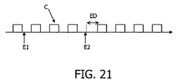
図21は、イベント駆動型の同期のためのタイミング信号の表現を示す。図21に示されるクロックCは、遅延ライン及びインバータDLIにより生成される。イベントE1がクロックのエッジよりも十分前に到達した場合、クロックCは遅延されない。なぜなら、準安定を回避するため、相互排斥ユニットmutexが該イベント及び離れたクロックエッジを受信するからである(イベントは最小の(一定の)時間内で発生する)。入力されるイベントE2がクロックエッジ近くで到達する場合にのみ(同時に、制限内で)、相互排斥要素が、何が最初に到達したか(又は厳密な一致の場合には何が最初に通過を許可されたか)を調停する必要がある。このことは(準安定のため)幾分かの時間を要し得、それ故クロックを遅延(ED)させ得る(即ち図14の第2のイベント)。このことは稀にしか起こらない。クロックが遅延された瞬間同士の間の時間は計算されることができ、IP及びNIのクロック速度に依存する(速くなるほど減少する)。 FIG. 21 shows a timing signal representation for event driven synchronization. The clock C shown in FIG. 21 is generated by the delay line and the inverter DLI. If event E1 arrives well before the clock edge, clock C is not delayed. This is because, in order to avoid metastability, the mutual exclusion unit mutex receives the event and the distant clock edge (the event occurs within a minimum (constant) time). Only when the incoming event E2 arrives close to the clock edge (at the same time, within the limits) what the mutual exclusion element has reached first (or what exactly passes in the case of an exact match) It is necessary to mediate. This can take some time (due to metastability) and therefore delay the clock (ED) (ie the second event in FIG. 14). This rarely happens. The time between the instants when the clock is delayed can be calculated and depends on the IP and NI clock speeds (decreasing with increasing speed).
応答経路は同様の態様で動作する。要求及び応答経路は、NIが一時停止可能(ただし短い時間の間のみ)であること(即ちローカルクロックが停止させられ得ること)を確実にするために、このように実装される。NIのみが停止させられ、結合されたいずれのルータのクロックも停止させられず、要求駆動型のハンドシェークのみが僅かに長く費やしても良いことは留意されたい。短い時間の間停止させられたNIが高速なルータに接続されている場合(例えば処理の変形又は温度差によって)、NIの瞬間的な失速は、ルータによって補償され得る。このようにして、分散非同期ネットワークオンチップNOCは、失速したNIによる全ての遅延流入が補償されることができないグローバルなクロックの同期ネットワークよりも、一時停止に対して優れた対応をすることができる。このことは待ち時間にのみ影響を与えスループットには影響を与えず、スループットは常に最も低速のフィードバックループへと減少させられる。 The response path operates in a similar manner. The request and response path is implemented in this way to ensure that the NI can be paused (but only for a short time) (ie the local clock can be stopped). Note that only the NI is stopped, the clocks of any combined routers are not stopped, and only the request driven handshake may be spent slightly longer. If a NI that has been stopped for a short period of time is connected to a fast router (eg, due to processing variations or temperature differences), the NI stall may be compensated by the router. In this way, the distributed asynchronous network-on-chip NOC can respond better to a pause than a global clock synchronous network where all delay inflows due to stalled NI cannot be compensated. . This only affects latency, not throughput, which is always reduced to the slowest feedback loop.
このとき、上述したデータ駆動型同期の場合に比べて、エラーのような入力されてくるイベントによるクロックの遅延を考慮すると、これらのエラーは合算されない。即ち、複数のNIが同時に遅延された場合、これら遅延の合計ではなく、これらの遅延のうち最も大きい遅延によってのみ、ネットワークオンチップNOC全体が遅延される。このことは、データ駆動型方式に対するイベント駆動型同期方式の利点である。 At this time, compared with the case of the data driven type synchronization described above, these errors are not summed up in consideration of a clock delay due to an input event such as an error. That is, when a plurality of NIs are delayed at the same time, the entire network-on-chip NOC is delayed only by the largest delay among these delays, not the sum of these delays. This is an advantage of the event-driven synchronization method over the data-driven method.
NI速度を例えば5%大きくすると、単一のクロック期間についての平均故障間隔は減少させられる。なぜなら、相互排斥要素mutexが安定化するために5%の付加的な時間が利用可能となるからである。複数の(例えば3個の)連続するクロック期間が考慮される場合、NIが1クロック期間の後に低速になり過ぎる確率よりも、NIが3クロック期間の後に低速になり過ぎる確率のほうが低い。なぜなら、1つの遅延イベントが3クロック期間で発生する場合、5%ではなく3×5%の安定化のためのたるみ(slack)を持つからである。3つの期間の間に2つの遅延イベントがある場合にも同様である(それぞれ1.5×5%のたるみを持つ)。3つの遅延イベントについて、付加的なたるみは利用可能ではない。このことは、データ駆動型方式に対するイベント駆動型同期方式の利点である。 Increasing the NI speed, for example by 5%, reduces the average failure interval for a single clock period. This is because 5% additional time is available to stabilize the mutual exclusion element mutex. When multiple (eg, three) consecutive clock periods are considered, the probability that NI is too slow after three clock periods is lower than the probability that NI is too slow after one clock period. This is because if one delay event occurs in 3 clock periods, it has a 3 × 5% stabilization slack instead of 5%. The same is true if there are two delay events between the three periods (each with a sag of 1.5 × 5%). For the three delay events, no additional sag is available. This is an advantage of the event-driven synchronization method over the data-driven method.
従って、ネットワークオンチップNOCの物理的な(タイミング及びクロック)側面は緩和される。即ち、ネットワークオンチップNOCのためのグローバルなクロックが必要とされない。ネットワークオンチップNOCは、構成要素の数という点で、即ち性能という点で、よりスケーラブルである。IP及びネットワークオンチップNOCは、(イベント駆動型IPNOC同期については)不正確なデータの虞なく、一方で失われた時間デッドラインの点で先験的に既知の平均故障間隔を伴い、任意の独立した速度で動作することができる。 Therefore, the physical (timing and clock) aspects of the network on chip NOC are relaxed. That is, no global clock for the network on chip NOC is required. Network-on-chip NOCs are more scalable in terms of the number of components, that is, in terms of performance. IP and network-on-chip NOCs (for event-driven IPNOC synchronization) do not have the risk of inaccurate data, while with a mean time interval known a priori in terms of lost time deadlines, any Can operate at independent speed.
一方で、非同期回路のテストは、同期回路についてのテストよりも困難となる。標準的なハードウェアバックエンドフロー(合成、タイミング確認等)は、非同期設計ではなく同期設計に、より適合される。 On the other hand, testing of asynchronous circuits is more difficult than testing of synchronous circuits. Standard hardware backend flows (synthesis, timing verification, etc.) are more adapted to synchronous design rather than asynchronous design.
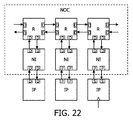
図22は、第6の実施例による、幾つかのIPブロックを結合するネットワークオンチップを示す。ネットワークインタフェースとルータとの間の通信及びルータ間通信は、D型ポートを用いたD型インタフェースに基づく。即ち、ネットワークオンチップの構成要素間のインタフェースは、要求駆動型である。それぞれのIPブロックと関連するネットワークインタフェースとの間のインタフェースは、第3(左)、第4(中)及び第5(右)の実施例によるインタフェースを呈する。従って、第3、第4及び第5の実施例によるインタフェースが、単一のネットワークオンチップにおいても適用されることができる。 FIG. 22 shows a network-on-chip combining several IP blocks according to a sixth embodiment. Communication between the network interface and the router and communication between routers are based on a D-type interface using a D-type port. That is, the interface between network on-chip components is request driven. The interface between each IP block and the associated network interface presents an interface according to the third (left), fourth (middle) and fifth (right) embodiments. Therefore, the interfaces according to the third, fourth and fifth embodiments can be applied even in a single network on chip.
第5の実施例による導入されたGALS技術に基づくネットワークオンチップNOCにおいて、NOCとIPとの間に要求駆動型通信を実装するため、NIとIPとの間のチャネルの両側においてD型ポートが利用される。全てのチャネルがD型のポートを利用するため、全てのブロックの整合のとれた進行が保証される。D型ポートは100%決定論的であるため、結果の性能もまた決定論的である。 In the network-on-chip NOC based on the introduced GALS technology according to the fifth embodiment, in order to implement request-driven communication between NOC and IP, D-type ports are provided on both sides of the channel between NI and IP. Used. Since all channels use D-type ports, a consistent progression of all blocks is guaranteed. Since the D-type port is 100% deterministic, the resulting performance is also deterministic.
QoSを提供するための他の方法(一般的なネットワークからの)が文献から知られている(特にH. Zhangによる「Service disciplines for guaranteed performance service in packet-switching networks」(IEEEのProceeding、83(10):1374-96、1995年10月)に記載されたようなレート制御された方式、及びJ. Rexfordによる「Tailoring Router Architectures to Performance Requirements in Cut-Through Networks」(PhD論文、University of Michigan、Department of Computer Science and Engineering、1999年)に記載されたようなデッドラインベースの方式)が、これらの方式を実装したネットワークオンチップNOCは報告されていない。これらの方法はまた、グローバルな同期の基準に依存している。 Other methods (from common networks) for providing QoS are known from the literature (especially “Service disciplines for guaranteed performance service in packet-switching networks” by H. Zhang (IEEE Proceeding, 83 ( 10): 1374-96, October 1995), and “Tailoring Router Architectures to Performance Requirements in Cut-Through Networks” by J. Rexford (PhD paper, University of Michigan, However, no network-on-chip NOC that implements these methods has been reported, as described in the Department of Computer Science and Engineering (1999)). These methods also rely on global synchronization criteria.
上述の実施例は本発明を限定するものではなく説明するものであって、当業者は添付する請求項の範囲から逸脱することなく多くの代替実施例を設計することが可能であろうことは留意されるべきである。請求項において、括弧に挟まれたいずれの参照記号も、請求の範囲を限定するものとして解釈されるべきではない。「有する(comprising)」なる語は、請求項に記載されたもの以外の要素又はステップの存在を除外するものではない。要素に先行する「1つの(a又はan)」なる語は、複数の斯かる要素の存在を除外するものではない。幾つかの手段を列記した装置請求項において、これら手段の幾つかは同一のハードウェアのアイテムによって実施化されても良い。特定の手段が相互に異なる従属請求項に列挙されているという単なる事実は、これら手段の組み合わせが有利に利用されることができないことを示すものではない。 The above-described embodiments are illustrative rather than limiting, and it will be appreciated by those skilled in the art that many alternative embodiments can be designed without departing from the scope of the appended claims. It should be noted. In the claims, any reference signs placed between parentheses shall not be construed as limiting the claim. The word “comprising” does not exclude the presence of elements or steps other than those listed in a claim. The word “a” or “an” preceding an element does not exclude the presence of a plurality of such elements. In the device claim enumerating several means, several of these means may be embodied by one and the same item of hardware. The mere fact that certain measures are recited in mutually different dependent claims does not indicate that a combination of these measured cannot be used to advantage.
更に、請求項におけるいずれの参照記号も、請求の範囲を限定するものと解釈されるべきではない。 Moreover, any reference signs in the claims shall not be construed as limiting the scope.
Claims (19)
それぞれが前記複数の第1の共有されたリソースの少なくとも1つについて調停を実行するための複数の調停ユニットと、
を有する電子装置であって、前記調停ユニット間の通信は非同期に実行され、前記第1の共有されたリソース間のデータ通信は非同期に実行され、
各前記調停ユニットは、第1のグローバルな時間の基準を実装するため、少なくとも1つの隣接する調停ユニットに第1のトークンを送信し、少なくとも1つの隣接する調停ユニットから第2のトークンを受信するように構成された、電子装置。 A plurality of first shared resources;
A plurality of arbitration units each for performing arbitration on at least one of the plurality of first shared resources;
The communication between the arbitration units is performed asynchronously, the data communication between the first shared resources is performed asynchronously,
Each said arbitration unit transmits a first token to at least one adjacent arbitration unit and receives a second token from at least one adjacent arbitration unit to implement a first global time reference An electronic device configured as described above.
前記複数のポートを結合するための第1の共有されたリソースである非同期相互接続手段と、
を更に有し、前記相互接続手段は、それぞれが第2の共有されたリソースである複数の相互接続ユニットと、複数の調停ユニットと、を有し、前記複数の調停ユニットのそれぞれは、複数の前記第2の共有されたリソースの少なくとも1つについて調停を実行し、前記相互接続手段内の第2のグローバルな時間の基準を実装するため、少なくとも1つの隣接する調停ユニットへ第1のトークンを送信し、少なくとも1つの隣接する調停ユニットから第2のトークンを受信する、請求項1に記載の電子装置。 Multiple ports,
An asynchronous interconnect means being a first shared resource for combining the plurality of ports;
The interconnection means includes a plurality of interconnection units, each of which is a second shared resource, and a plurality of arbitration units, wherein each of the plurality of arbitration units includes a plurality of A first token to at least one adjacent arbitration unit to perform arbitration on at least one of the second shared resources and implement a second global time reference in the interconnection means; The electronic device of claim 1, wherein the electronic device transmits and receives a second token from at least one adjacent arbitration unit.
複数の第1の共有されたリソースの少なくとも1つについて複数の調停を実行するステップを有し、
前記調停間の通信は非同期に実行され、前記共有されたリソース間のデータ通信は非同期に実行され、
各前記調停するステップは、第1のグローバルな時間の基準を実装するため、少なくとも1つの隣接する調停に第1のトークンを送信するステップと、少なくとも1つの隣接する調停から第2のトークンを受信するステップと、を有する方法。 A method for arbitrating a shared resource in an electronic device having a plurality of shared resources, the method comprising:
Performing a plurality of arbitrations for at least one of the plurality of first shared resources;
Communication between the arbitrations is executed asynchronously, data communication between the shared resources is executed asynchronously,
Each said arbitrating step transmits a first token to at least one adjacent arbitration and receives a second token from at least one adjacent arbitration to implement a first global time reference. And a step comprising:
Applications Claiming Priority (2)
| Application Number | Priority Date | Filing Date | Title |
|---|---|---|---|
| EP05101716 | 2005-03-04 | ||
| PCT/IB2006/050649 WO2006092768A1 (en) | 2005-03-04 | 2006-03-02 | Electronic device and a method for arbitrating shared resources |
Publications (1)
| Publication Number | Publication Date |
|---|---|
| JP2008532169A true JP2008532169A (en) | 2008-08-14 |
Family
ID=36571017
Family Applications (1)
| Application Number | Title | Priority Date | Filing Date |
|---|---|---|---|
| JP2007557657A Withdrawn JP2008532169A (en) | 2005-03-04 | 2006-03-02 | Electronic device and method for arbitrating shared resources |
Country Status (5)
| Country | Link |
|---|---|
| US (1) | US20080215786A1 (en) |
| EP (1) | EP1859575A1 (en) |
| JP (1) | JP2008532169A (en) |
| CN (1) | CN101133597A (en) |
| WO (1) | WO2006092768A1 (en) |
Families Citing this family (16)
| Publication number | Priority date | Publication date | Assignee | Title |
|---|---|---|---|---|
| JP2010500641A (en) * | 2006-08-08 | 2010-01-07 | コーニンクレッカ フィリップス エレクトロニクス エヌ ヴィ | Electronic device and communication synchronization method |
| WO2008038235A2 (en) * | 2006-09-27 | 2008-04-03 | Ecole Polytechnique Federale De Lausanne (Epfl) | Method to manage the load of peripheral elements within a multicore system |
| US7962786B2 (en) * | 2006-11-17 | 2011-06-14 | Nokia Corporation | Security features in interconnect centric architectures |
| EP2026493A1 (en) * | 2007-08-16 | 2009-02-18 | STMicroelectronics S.r.l. | Method and systems for mesochronous communications in multiple clock domains and corresponding computer program product |
| WO2009072038A2 (en) * | 2007-12-05 | 2009-06-11 | Nxp B.V. | Source-synchronous data link for system-on-chip design |
| US20090307408A1 (en) * | 2008-06-09 | 2009-12-10 | Rowan Nigel Naylor | Peer-to-Peer Embedded System Communication Method and Apparatus |
| US8543750B1 (en) | 2008-10-15 | 2013-09-24 | Octasic Inc. | Method for sharing a resource and circuit making use of same |
| US8689218B1 (en) | 2008-10-15 | 2014-04-01 | Octasic Inc. | Method for sharing a resource and circuit making use of same |
| US8270316B1 (en) * | 2009-01-30 | 2012-09-18 | The Regents Of The University Of California | On-chip radio frequency (RF) interconnects for network-on-chip designs |
| US8631213B2 (en) | 2010-09-16 | 2014-01-14 | Apple Inc. | Dynamic QoS upgrading |
| US8314807B2 (en) | 2010-09-16 | 2012-11-20 | Apple Inc. | Memory controller with QoS-aware scheduling |
| US9053058B2 (en) | 2012-12-20 | 2015-06-09 | Apple Inc. | QoS inband upgrade |
| US9229896B2 (en) | 2012-12-21 | 2016-01-05 | Apple Inc. | Systems and methods for maintaining an order of read and write transactions in a computing system |
| US10027433B2 (en) * | 2013-06-19 | 2018-07-17 | Netspeed Systems | Multiple clock domains in NoC |
| US9740235B1 (en) * | 2015-03-05 | 2017-08-22 | Liming Xiu | Circuits and methods of TAF-DPS based interface adapter for heterogeneously clocked Network-on-Chip system |
| SG10201600276YA (en) * | 2016-01-14 | 2017-08-30 | Huawei Int Pte Ltd | Device, method and system for routing global assistant signals in a network-on-chip |
Family Cites Families (13)
| Publication number | Priority date | Publication date | Assignee | Title |
|---|---|---|---|---|
| US5689644A (en) * | 1996-03-25 | 1997-11-18 | I-Cube, Inc. | Network switch with arbitration sytem |
| DE19620137C2 (en) * | 1996-05-07 | 2000-08-24 | Daimler Chrysler Ag | Protocol for security-critical applications |
| US5978578A (en) * | 1997-01-30 | 1999-11-02 | Azarya; Arnon | Openbus system for control automation networks |
| US6487213B1 (en) * | 1998-01-05 | 2002-11-26 | Polytechnic University | Methods and apparatus for fairly arbitrating contention for an output port |
| US6449283B1 (en) * | 1998-05-15 | 2002-09-10 | Polytechnic University | Methods and apparatus for providing a fast ring reservation arbitration |
| GB2374242B (en) * | 2001-04-07 | 2005-03-16 | Univ Dundee | Integrated circuit and related improvements |
| US7076595B1 (en) * | 2001-05-18 | 2006-07-11 | Xilinx, Inc. | Programmable logic device including programmable interface core and central processing unit |
| FI115015B (en) * | 2002-04-22 | 2005-02-15 | Metso Automation Oy | Procedure and system for securing a bus and control server |
| US7239669B2 (en) * | 2002-04-30 | 2007-07-03 | Fulcrum Microsystems, Inc. | Asynchronous system-on-a-chip interconnect |
| KR100488478B1 (en) * | 2002-10-31 | 2005-05-11 | 서승우 | Multiple Input/Output-Queued Switch |
| DE10303673A1 (en) * | 2003-01-24 | 2004-08-12 | IHP GmbH - Innovations for High Performance Microelectronics/Institut für innovative Mikroelektronik | Asynchronous envelope for a globally asynchronous, locally synchronous (GALS) circuit |
| US7467358B2 (en) * | 2004-06-03 | 2008-12-16 | Gwangju Institute Of Science And Technology | Asynchronous switch based on butterfly fat-tree for network on chip application |
| US8619554B2 (en) * | 2006-08-04 | 2013-12-31 | Arm Limited | Interconnecting initiator devices and recipient devices |
-
2006
- 2006-03-02 CN CNA2006800071212A patent/CN101133597A/en active Pending
- 2006-03-02 WO PCT/IB2006/050649 patent/WO2006092768A1/en not_active Application Discontinuation
- 2006-03-02 EP EP06711001A patent/EP1859575A1/en not_active Withdrawn
- 2006-03-02 JP JP2007557657A patent/JP2008532169A/en not_active Withdrawn
- 2006-03-02 US US11/817,060 patent/US20080215786A1/en not_active Abandoned
Also Published As
| Publication number | Publication date |
|---|---|
| EP1859575A1 (en) | 2007-11-28 |
| US20080215786A1 (en) | 2008-09-04 |
| CN101133597A (en) | 2008-02-27 |
| WO2006092768A1 (en) | 2006-09-08 |
Similar Documents
| Publication | Publication Date | Title |
|---|---|---|
| JP2008532169A (en) | Electronic device and method for arbitrating shared resources | |
| US7940666B2 (en) | Communication node architecture in a globally asynchronous network on chip system | |
| US10027433B2 (en) | Multiple clock domains in NoC | |
| US8352774B2 (en) | Inter-clock domain data transfer FIFO circuit | |
| US7925803B2 (en) | Method and systems for mesochronous communications in multiple clock domains and corresponding computer program product | |
| Agarwal et al. | Survey of network on chip (noc) architectures & contributions | |
| Dall'Osso et al. | Xpipes: a latency insensitive parameterized network-on-chip architecture for multi-processor SoCs | |
| US10355851B2 (en) | Methods and systems for synchronization between multiple clock domains | |
| CN101278528A (en) | Subscriber and communication controller of a communication system and method for implementing a gateway functionality in a subscriber of a communication system | |
| Hansson et al. | Enabling application-level performance guarantees in network-based systems on chip by applying dataflow analysis | |
| CN111971648A (en) | Asynchronous multi-clock domain data stream splicing and resynchronization system and method | |
| Chen et al. | ArSMART: An improved SMART NoC design supporting arbitrary-turn transmission | |
| US7792030B2 (en) | Method and system for full-duplex mesochronous communications and corresponding computer program product | |
| Ueter et al. | Simultaneous progressing switching protocols for timing predictable real-time network-on-chips | |
| WO2013101794A1 (en) | Link between chips using virtual channels and credit based flow control | |
| Yang et al. | NISAR: An AXI compliant on-chip NI architecture offering transaction reordering processing | |
| Song et al. | Asynchronous spatial division multiplexing router | |
| Gibiluka et al. | BAT-Hermes: a transition-signaling bundled-data NoC router | |
| Mekie et al. | Interface design for rationally clocked GALS systems | |
| CN114679423A (en) | Flow control mechanism-oriented deadlock-free extensible interconnected bare core structure | |
| Nambinina et al. | Extension of the lisnoc (network-on-chip) with an axi-based network interface | |
| Naqvi et al. | A multi-credit flow control scheme for asynchronous NoCs | |
| US11243856B1 (en) | Framing protocol supporting low-latency serial interface in an emulation system | |
| Sparso | Asynchronous design of networks-on-chip | |
| JP2002141922A (en) | Loop type path system |
Legal Events
| Date | Code | Title | Description |
|---|---|---|---|
| A300 | Application deemed to be withdrawn because no request for examination was validly filed |
Free format text: JAPANESE INTERMEDIATE CODE: A300 Effective date: 20090512 |