EP1723781B1 - Imaging system with adjusted dark floor correction - Google Patents
Imaging system with adjusted dark floor correction Download PDFInfo
- Publication number
- EP1723781B1 EP1723781B1 EP05724769A EP05724769A EP1723781B1 EP 1723781 B1 EP1723781 B1 EP 1723781B1 EP 05724769 A EP05724769 A EP 05724769A EP 05724769 A EP05724769 A EP 05724769A EP 1723781 B1 EP1723781 B1 EP 1723781B1
- Authority
- EP
- European Patent Office
- Prior art keywords
- dark
- dark floor
- floor values
- image
- values
- Prior art date
- Legal status (The legal status is an assumption and is not a legal conclusion. Google has not performed a legal analysis and makes no representation as to the accuracy of the status listed.)
- Active
Links
- 238000012937 correction Methods 0.000 title description 19
- 238000003384 imaging method Methods 0.000 title description 10
- 238000000034 method Methods 0.000 claims description 53
- 230000008569 process Effects 0.000 claims description 12
- 230000006870 function Effects 0.000 claims description 11
- 238000012545 processing Methods 0.000 claims description 9
- 230000002123 temporal effect Effects 0.000 claims description 3
- 238000012935 Averaging Methods 0.000 claims 1
- 230000007547 defect Effects 0.000 description 35
- 230000002950 deficient Effects 0.000 description 20
- 238000010586 diagram Methods 0.000 description 9
- 230000009471 action Effects 0.000 description 7
- 238000003672 processing method Methods 0.000 description 7
- 230000003190 augmentative effect Effects 0.000 description 5
- 230000004044 response Effects 0.000 description 3
- 230000000694 effects Effects 0.000 description 2
- 230000007613 environmental effect Effects 0.000 description 2
- 230000007246 mechanism Effects 0.000 description 2
- 238000013459 approach Methods 0.000 description 1
- 230000008859 change Effects 0.000 description 1
- 238000006243 chemical reaction Methods 0.000 description 1
- 239000003574 free electron Substances 0.000 description 1
- 238000005259 measurement Methods 0.000 description 1
- 238000012986 modification Methods 0.000 description 1
- 230000004048 modification Effects 0.000 description 1
- 230000003287 optical effect Effects 0.000 description 1
- 238000012552 review Methods 0.000 description 1
- 230000009897 systematic effect Effects 0.000 description 1
Images


Classifications
-
- H—ELECTRICITY
- H04—ELECTRIC COMMUNICATION TECHNIQUE
- H04N—PICTORIAL COMMUNICATION, e.g. TELEVISION
- H04N25/00—Circuitry of solid-state image sensors [SSIS]; Control thereof
- H04N25/60—Noise processing, e.g. detecting, correcting, reducing or removing noise
- H04N25/63—Noise processing, e.g. detecting, correcting, reducing or removing noise applied to dark current
-
- H—ELECTRICITY
- H04—ELECTRIC COMMUNICATION TECHNIQUE
- H04N—PICTORIAL COMMUNICATION, e.g. TELEVISION
- H04N25/00—Circuitry of solid-state image sensors [SSIS]; Control thereof
- H04N25/60—Noise processing, e.g. detecting, correcting, reducing or removing noise
- H04N25/67—Noise processing, e.g. detecting, correcting, reducing or removing noise applied to fixed-pattern noise, e.g. non-uniformity of response
- H04N25/671—Noise processing, e.g. detecting, correcting, reducing or removing noise applied to fixed-pattern noise, e.g. non-uniformity of response for non-uniformity detection or correction
-
- H—ELECTRICITY
- H04—ELECTRIC COMMUNICATION TECHNIQUE
- H04N—PICTORIAL COMMUNICATION, e.g. TELEVISION
- H04N25/00—Circuitry of solid-state image sensors [SSIS]; Control thereof
- H04N25/60—Noise processing, e.g. detecting, correcting, reducing or removing noise
- H04N25/68—Noise processing, e.g. detecting, correcting, reducing or removing noise applied to defects
Definitions
- This invention relates generally to electronic imaging systems and, more particularly, to methods and apparatus for removing the dark floor from a captured image.
- Image sensors generally exhibit a phenomenon known as dark signal in which an image signal is detected even in the absence of light.
- the amount of dark signal varies in a random fashion from pixel to pixel in the image sensor, and the dark signal is sensitive to environmental conditions, notably temperature, but the base level of dark signal for a given pixel is reasonably consistent for a given image capture condition.
- One typical approach to removing the dark signal is to capture a dark frame, an image captured with the shutter closed, in close temporal proximity to the actual image capture (called a contemporary dark frame). This contemporary dark frame is then subtracted on a pixel by pixel basis from the actual image.
- One shortcoming of this method is that there is a level of noise in the dark signal, so the noise in the dark signal in the image will add (in some fashion related to the noise distribution) to the noise in the dark signal of the dark frame, thereby increasing the noise in the final processed image at the same time the base level dark signal is removed.
- a further shortcoming is that the dark frame capture should have the same conditions as the actual image capture, notably exposure time. Hence, for a long exposure time in which the dark signal has a long time to accumulate, the dark frame exposure time will have to be equally long, doubling the amount of time required to capture an image.
- An alternative method for dark signal removal involves capturing a series of dark frames under some nominal conditions during a calibration process, perhaps at the time the electronic imaging system is manufactured.
- the series of dark frames is averaged together, thereby significantly reducing the noise component of the dark signal.
- This averaged dark frame is stored in a non-volatile memory and used as a baseline dark floor. Since the dark signal is sensitive to environmental and image capture conditions, the baseline dark floor would only be useful if the temperature and exposure time of an actual image capture matched the conditions under which the calibrated dark frames were captured.
- An image sensor generally has light shielded pixels that are used for general offset correction in image processing; the dark pixels from the actual image capture can be compared to the dark pixels from the baseline dark floor, and the result of the comparison can be used to adjust the baseline dark floor to match better the conditions of the actual image capture. This adjusted baseline dark floor is subtracted from the actual image. Although this reduces the additional noise and capture time associated with the previous dark floor removal method, it does have some shortcomings: the dark pixels are not uniformly distributed throughout the image sensor, so regional variations in the temperature of the sensor would not be detected; and some pixels may have a dark signal that behaves abnormally with respect to temperature or exposure time, so the baseline dark floor will not be adjusted correctly for those pixels.
- the present invention is directed to overcoming one or more of the problems set forth above.
- the invention provides a method for utilizing both a dark frame captured contemporaneously with the capture of an actual image and a stored, calibrated dark floor in order to provide a reduced noise, adjusted dark floor that can be subtracted from the image.
- the stored calibrated dark floor is used as a baseline dark floor that includes an average of a series of captured dark frames.
- the contemporary dark frame can be a function of the most recent captured dark frame and the stored baseline dark floor in order to improve the contemporary dark frame.
- the same stored baseline dark floor along with newly captured contemporary dark frames are used to compute the adjusted dark floor.
- a calibrated map of defective pixels can be used during the process of adjusting the dark floor to avoid defective pixels and thereby to improve the adjustment process.
- the process of adjusting the dark floor can also be used to identify pixels that have become faulty with time or due to capture conditions and these newly identified defective pixels can be used to adjust the defective pixel map.
- the adjusted defective pixel map can be used during the process of adjusting the dark floor at some subsequent time.
- the present invention has the advantages of removing the dark floor from a captured image without introducing other artifacts.
- an electronic imaging system has an optical assembly comprising the image sensor 1 which is exposed to light that first passes through the lens 2 and the shutter mechanism 3. As the sensor 1 is exposed to light, free electrons are generated and captured within the sensor's electronic structure. The resulting electronic charge at each pixel location is converted to a voltage which is digitized by the analog-to-digital converter 4 and the resulting data is stored in the raw image memory 5.
- a contemporary dark frame When a contemporary dark frame is generated, it first comes to the processor 6 by way of the raw image memory 5. The processor 6 can then move the dark frame to the contemporary dark frame memory 7. It is also possible that the electronic imaging system has a baseline dark floor memory 9. If so, the processor 6 can use the contemporary dark frame and the baseline dark floor to produce an adjusted dark floor which is stored in the adjusted dark floor memory 10.
- the electronic imaging system has a baseline defect map memory 11 which holds a list of sensor defects that must be corrected for each image. If so, the processor 6 can use the contemporary dark frame and the baseline defect map to produce an adjusted defect map which is stored in the adjusted defect map memory 12. In addition, it is possible for the electronic imaging system to have a processed image storage 8 that can used to store intermediate and final output from the processor 6.
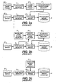
- FIG. 2a One well known method of accounting for dark current, shown in FIG. 2a , begins with a dark frame capture 20 that causes the dark frame data to be stored in the raw image memory 5. The next action is to store the dark frame 21 which moves the data from the raw image memory 5 to the contemporary dark frame memory 7. The next step is to capture an image 22, which puts the image data into the raw image memory 5. The action of processing the image 23 can now occur wherein the image data from the raw image memory 5 is combined with the contemporary dark frame data from the contemporary dark frame memory 7 to produce results that are stored in the processed image storage 8.
- FIG. 2b Another well known method of accounting for dark current, shown in FIG. 2b , begins with an image capture 22, which puts the image data into the raw image memory 5. The next step is to adjust the baseline dark floor 24, which takes data from the raw image memory 5 and from the baseline dark floor memory 9 to produce results which are put into the adjusted dark floor memory 10. The action of processing the image 23 can now occur wherein the image data from the raw image memory 5 is combined with the adjusted dark floor data from the adjusted dark floor memory 10 to produce results that are stored in the processed image storage 8.
- a well known method of accounting for sensor defects begins with an image capture 22, which puts the image data into the raw image memory 5.
- the next step is to process the image 23, which takes data from the baseline defect map memory 11 data and from the raw image memory 5, to produce results which are put into the processed image storage 8.
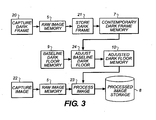
- the present invention addresses the problem that the contemporary dark frame has unwanted noise.
- One method of the present invention begins with a dark frame capture 20, which puts the dark frame image data into the raw image memory 5.
- the next step is to store the dark frame 21, which takes the data from the raw image memory 5 and puts it into the contemporary dark frame memory 7.
- the action of adjusting the baseline dark floor 24 can now occur wherein the baseline dark floor image data, taken from the baseline dark floor memory 9, is scaled in response to the statistics of the contemporary dark frame image data, which is taken from the contemporary dark frame memory 7.
- the scaled baseline dark floor image data is then compared on a pixel-by-pixel basis to the contemporary dark frame.
- the scaled dark floor image data is stored in the adjusted dark floor memory 10; if there is a sufficiently large difference between the scaled baseline dark floor image data and the contemporary dark frame data, then the contemporary dark frame data is stored in the adjusted dark floor memory 10.
- the function that selects between the scaled baseline dark floor memory and the contemporary dark frame data could simply select from one or the other based on comparing the difference between the two to a threshold limit value.
- the threshold could be based on the expected noise statistics of the contemporary dark frame data: if the difference is within the expected noise, the scaled baseline dark floor is chosen, but if the difference is greater than the expected noise then the contemporary dark frame data is chosen.
- the function could provide a weighted average of the values from the adjusted baseline dark floor memory and the contemporary dark frame data, wherein the weighting is a function of the difference between the two values.
- the image data is stored in the raw image memory 5.
- the action of the image processing 23 now occurs wherein the image data is taken from the raw image memory 5 and combined with the adjusted dark floor image data, which is taken from the adjusted dark floor memory 10, to produce results that are stored in the processed image storage 8.
- the method just described is very simple to implement, it is unresponsive to local variations in operating conditions for the sensor, notably local variations in temperature; to the extent that these local variations render incorrect the scale factor applied globally to the baseline dark floor, the method will erroneously favor the contemporary dark frame.
- Another method of the present invention addresses this shortcoming by adjusting the baseline dark floor image data in response to the local statistics of the contemporary dark frame image data. Referring again to FIG. 3 , this alternative process of adjusting the baseline dark floor 24 is now disclosed.
- the contemporary dark frame data is a direct measurement of dark current noise under current conditions. Because there are often local thermal gradients, a correction scale factor needs to be determined at a number of positions on the sensor face.
- the correction scale factor can be interpolated at each pixel location using a standard interpolation method such as bicubic interpolation.
- the adjusted dark floor image data is then produced by multiplying, at each pixel location, the dark floor pixel value M by the pixel correction scale factor ⁇ .
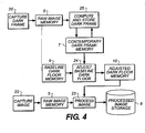
- FIG. 4 an augmented form of the method of FIG. 3 is shown.
- the augmented method begins with a dark frame capture 20, which puts the dark frame image data into the raw image memory 5.
- the next step is to compute and store the dark frame 25 wherein the data from the raw image memory 5 and existing contemporary dark frame data, taken from the contemporary dark frame memory 7, are combined and put back into the contemporary dark frame memory 7. Multiple dark frame capture may be made at this time if so desired.
- the action of adjusting the baseline dark floor 24 can now occur and the remaining steps in FIG. 4 are identical to those shown in FIG. 3 .
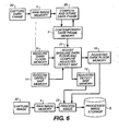
- FIG. 5 an augmented form of the method of FIG. 4 is shown.
- the method shown in FIG. 5 is identical to that of FIG. 4 up to the step of adjusting the baseline dark floor 24, wherein the baseline dark floor image data, taken from the baseline dark floor memory 9, is locally adjusted in response jointly to the local statistics of the contemporary dark frame image data, taken from the contemporary dark frame memory 7, and to the baseline defect map data, taken from the baseline defect map memory 11.
- the adjusted baseline dark floor image data is then stored in the adjusted dark floor memory 10.
- the image data is stored in the raw image memory 5.
- the action of the image processing 23 now occurs wherein the image data is taken from the raw image memory 5 and combined jointly with the adjusted dark floor image data, taken from the adjusted dark floor memory 10, and with the baseline defect map data, taken from the baseline defect map memory 11, to produce results that are stored in the processed image storage 8.
- the role of the baseline defect map data is now disclosed.
- the baseline defect map data identifies defective pixels known to produce unreliable image data.
- computing the statistics of a contemporary dark frame excludes data from the defective pixels.
- raw image data from these same defective pixels are corrected before being used to form the processed image data which is stored in the processed image storage 8.
- FIG. 6 an augmented form of the method of FIG. 5 is shown.
- the method shown in FIG. 6 is identical to that of FIG. 5 up through the step of compute and store dark frame 25.
- a new step, adjusting the baseline dark floor and computing the adjusted defect map 27, is performed wherein the baseline dark floor data and the baseline defect map data are jointly adjusted to produce results that are stored in the adjusted dark floor memory 10 and the adjusted defect map memory 12, respectively.
- the final step of processing the image 23 now uses adjusted defect map data, taken from the adjusted defect map memory 12, instead of baseline defect map data, taken from baseline defect map memory 11, as was the case in FIG. 5 .
- FIG. 7 an augmented form of the method of FIG. 6 is shown.
- the method shown in FIG. 7 is identical to that of FIG. 6 except that the step of adjusting the baseline dark floor and computing the adjusted defect map 27 also uses the adjusted defect map data from a previous capture, taken from the adjusted defect map memory 12.
- the baseline defective map data identifies defective pixels that existed at some remote time in the past, such as when the camera was , calibrated. Since it is possible for some pixels to become defective after the baseline defect map was created, it is desirable to adjust the defect map to include the newly converted defective pixels. One method of discovering such a conversion is to notice a significant change in the contemporary dark frame noise statistics of a particular pixel.
- the adjusted defect map is more up to date than the baseline defect map and therefore better data.
Landscapes
- Engineering & Computer Science (AREA)
- Multimedia (AREA)
- Signal Processing (AREA)
- Image Processing (AREA)
- Image Input (AREA)
- Testing, Inspecting, Measuring Of Stereoscopic Televisions And Televisions (AREA)
- Transforming Light Signals Into Electric Signals (AREA)
Description
- This invention relates generally to electronic imaging systems and, more particularly, to methods and apparatus for removing the dark floor from a captured image.
- Electronic imaging systems often include a facility for removing the dark floor from a captured image. Image sensors generally exhibit a phenomenon known as dark signal in which an image signal is detected even in the absence of light. The amount of dark signal varies in a random fashion from pixel to pixel in the image sensor, and the dark signal is sensitive to environmental conditions, notably temperature, but the base level of dark signal for a given pixel is reasonably consistent for a given image capture condition. One typical approach to removing the dark signal (as described for example by
US 6 163 339 ) is to capture a dark frame, an image captured with the shutter closed, in close temporal proximity to the actual image capture (called a contemporary dark frame). This contemporary dark frame is then subtracted on a pixel by pixel basis from the actual image. One shortcoming of this method is that there is a level of noise in the dark signal, so the noise in the dark signal in the image will add (in some fashion related to the noise distribution) to the noise in the dark signal of the dark frame, thereby increasing the noise in the final processed image at the same time the base level dark signal is removed. A further shortcoming is that the dark frame capture should have the same conditions as the actual image capture, notably exposure time. Hence, for a long exposure time in which the dark signal has a long time to accumulate, the dark frame exposure time will have to be equally long, doubling the amount of time required to capture an image. - An alternative method for dark signal removal involves capturing a series of dark frames under some nominal conditions during a calibration process, perhaps at the time the electronic imaging system is manufactured. The series of dark frames is averaged together, thereby significantly reducing the noise component of the dark signal. This averaged dark frame is stored in a non-volatile memory and used as a baseline dark floor. Since the dark signal is sensitive to environmental and image capture conditions, the baseline dark floor would only be useful if the temperature and exposure time of an actual image capture matched the conditions under which the calibrated dark frames were captured. An image sensor generally has light shielded pixels that are used for general offset correction in image processing; the dark pixels from the actual image capture can be compared to the dark pixels from the baseline dark floor, and the result of the comparison can be used to adjust the baseline dark floor to match better the conditions of the actual image capture. This adjusted baseline dark floor is subtracted from the actual image. Although this reduces the additional noise and capture time associated with the previous dark floor removal method, it does have some shortcomings: the dark pixels are not uniformly distributed throughout the image sensor, so regional variations in the temperature of the sensor would not be detected; and some pixels may have a dark signal that behaves abnormally with respect to temperature or exposure time, so the baseline dark floor will not be adjusted correctly for those pixels.
- The present invention is directed to overcoming one or more of the problems set forth above. Briefly summarized, according to one aspect of the present invention, the invention provides a method for utilizing both a dark frame captured contemporaneously with the capture of an actual image and a stored, calibrated dark floor in order to provide a reduced noise, adjusted dark floor that can be subtracted from the image. The stored calibrated dark floor is used as a baseline dark floor that includes an average of a series of captured dark frames. According to another aspect of the invention, the contemporary dark frame can be a function of the most recent captured dark frame and the stored baseline dark floor in order to improve the contemporary dark frame. The same stored baseline dark floor along with newly captured contemporary dark frames are used to compute the adjusted dark floor. According to another aspect of the invention, a calibrated map of defective pixels can be used during the process of adjusting the dark floor to avoid defective pixels and thereby to improve the adjustment process. According to another aspect of the invention, the process of adjusting the dark floor can also be used to identify pixels that have become faulty with time or due to capture conditions and these newly identified defective pixels can be used to adjust the defective pixel map. According to another aspect of the invention, the adjusted defective pixel map can be used during the process of adjusting the dark floor at some subsequent time.
- These and other aspects, objects, features and advantages of the present invention will be more clearly understood and appreciated from a review of the following detailed description of the preferred embodiments and appended claims, and by reference to the accompanying drawings.
- The present invention has the advantages of removing the dark floor from a captured image without introducing other artifacts.
-
-
Fig. 1 is a block diagram of an electronic imaging system; -
Fig. 2a (prior art) is a flow diagram of a typical image processing method including dark floor correction using a dark frame that is captured contemporaneously with an actual image capture; -
Fig. 2b (prior art) is a flow diagram of a typical image processing , method including dark floor correction using a dark floor that is captured and
stored during a calibration process at some time prior to the actual image capture, then adjusted based on the actual image capture data before being applied to the image; -
Fig. 2c (prior art) is a flow diagram of a typical image processing method including defective pixel correction using a defect map to identify defective pixels that is captured and stored during a calibration process at some time prior to the actual image capture; -
Fig. 3 is a flow diagram of an image processing method including dark floor correction that utilizes both a contemporary dark frame and a calibrated dark floor to create a new, adjusted dark floor; -
Fig. 4 is a flow diagram of an image processing method including dark floor correction that expands onFig. 3 by allowing the contemporary dark frame to be a function of a number of contemporary dark frame captures; -
Fig. 5 is a flow diagram of a image processing method including dark floor correction and defective pixel correction with the defective pixel correction used both to adjust the dark floor (to avoid using defective pixels in adjusting the dark floor) and to identify pixels requiring replacement in the image; -
Fig. 6 is a flow diagram of an image processing method including dark floor correction and defective pixel correction that expands onFig. 5 by allowing the calibrated defect map to be adjusted to include additional or different defective pixels identified during the dark floor adjustment process; and -
Fig. 7 is a flow diagram of an image processing method including dark floor correction and defective pixel correction that expands onFig. 6 by allowing the adjustment of the calibrated defect map to include knowledge of previous adjustments to the defect map. - Since electronic imaging systems are well known, the present description will be directed in particular to elements forming part of, or cooperating directly with, apparatus and method in accordance with the present invention. Elements not specifically shown or described herein may be selected from those known in the art.
- Referring initially to
FIG. 1 , an electronic imaging system has an optical assembly comprising the image sensor 1 which is exposed to light that first passes through thelens 2 and theshutter mechanism 3. As the sensor 1 is exposed to light, free electrons are generated and captured within the sensor's electronic structure. The resulting electronic charge at each pixel location is converted to a voltage which is digitized by the analog-to-digital converter 4 and the resulting data is stored in theraw image memory 5. - When a contemporary dark frame is generated, it first comes to the
processor 6 by way of theraw image memory 5. Theprocessor 6 can then move the dark frame to the contemporary dark frame memory 7. It is also possible that the electronic imaging system has a baselinedark floor memory 9. If so, theprocessor 6 can use the contemporary dark frame and the baseline dark floor to produce an adjusted dark floor which is stored in the adjusteddark floor memory 10. - Again, referring to
FIG. 1 , it is possible that the electronic imaging system has a baselinedefect map memory 11 which holds a list of sensor defects that must be corrected for each image. If so, theprocessor 6 can use the contemporary dark frame and the baseline defect map to produce an adjusted defect map which is stored in the adjusteddefect map memory 12. In addition, it is possible for the electronic imaging system to have a processedimage storage 8 that can used to store intermediate and final output from theprocessor 6. - One well known method of accounting for dark current, shown in
FIG. 2a , begins with adark frame capture 20 that causes the dark frame data to be stored in theraw image memory 5. The next action is to store the dark frame 21 which moves the data from theraw image memory 5 to the contemporary dark frame memory 7. The next step is to capture animage 22, which puts the image data into theraw image memory 5. The action of processing theimage 23 can now occur wherein the image data from theraw image memory 5 is combined with the contemporary dark frame data from the contemporary dark frame memory 7 to produce results that are stored in the processedimage storage 8. - Another well known method of accounting for dark current, shown in
FIG. 2b , begins with animage capture 22, which puts the image data into theraw image memory 5. The next step is to adjust the baselinedark floor 24, which takes data from theraw image memory 5 and from the baselinedark floor memory 9 to produce results which are put into the adjusteddark floor memory 10. The action of processing theimage 23 can now occur wherein the image data from theraw image memory 5 is combined with the adjusted dark floor data from the adjusteddark floor memory 10 to produce results that are stored in the processedimage storage 8. - A well known method of accounting for sensor defects, shown in
FIG. 2c , begins with animage capture 22, which puts the image data into theraw image memory 5. The next step is to process theimage 23, which takes data from the baselinedefect map memory 11 data and from theraw image memory 5, to produce results which are put into the processedimage storage 8. - Now, referring to
FIG. 3 , the present invention addresses the problem that the contemporary dark frame has unwanted noise. One method of the present invention begins with adark frame capture 20, which puts the dark frame image data into theraw image memory 5. The next step is to store the dark frame 21, which takes the data from theraw image memory 5 and puts it into the contemporary dark frame memory 7. The action of adjusting the baselinedark floor 24 can now occur wherein the baseline dark floor image data, taken from the baselinedark floor memory 9, is scaled in response to the statistics of the contemporary dark frame image data, which is taken from the contemporary dark frame memory 7. The scaled baseline dark floor image data is then compared on a pixel-by-pixel basis to the contemporary dark frame. To the extent that the scaled baseline dark floor image data matches the contemporary dark frame data, the scaled dark floor image data is stored in the adjusteddark floor memory 10; if there is a sufficiently large difference between the scaled baseline dark floor image data and the contemporary dark frame data, then the contemporary dark frame data is stored in the adjusteddark floor memory 10. The function that selects between the scaled baseline dark floor memory and the contemporary dark frame data could simply select from one or the other based on comparing the difference between the two to a threshold limit value. The threshold could be based on the expected noise statistics of the contemporary dark frame data: if the difference is within the expected noise, the scaled baseline dark floor is chosen, but if the difference is greater than the expected noise then the contemporary dark frame data is chosen. Alternatively, the function could provide a weighted average of the values from the adjusted baseline dark floor memory and the contemporary dark frame data, wherein the weighting is a function of the difference between the two values. After theimage capture 22, the image data is stored in theraw image memory 5. The action of theimage processing 23 now occurs wherein the image data is taken from theraw image memory 5 and combined with the adjusted dark floor image data, which is taken from the adjusteddark floor memory 10, to produce results that are stored in the processedimage storage 8. - Although the method just described is very simple to implement, it is unresponsive to local variations in operating conditions for the sensor, notably local variations in temperature; to the extent that these local variations render incorrect the scale factor applied globally to the baseline dark floor, the method will erroneously favor the contemporary dark frame. Another method of the present invention addresses this shortcoming by adjusting the baseline dark floor image data in response to the local statistics of the contemporary dark frame image data. Referring again to
FIG. 3 , this alternative process of adjusting the baselinedark floor 24 is now disclosed. The contemporary dark frame data is a direct measurement of dark current noise under current conditions. Because there are often local thermal gradients, a correction scale factor needs to be determined at a number of positions on the sensor face. Focusing on a single region for the moment, consider a small region of 32x32 pixels containing a total of 1024 pixels. Let Mk denote the value at the kth pixel (1 ≤ k ≤ 1024) stored in the baseline dark floor image data. Likewise, let Xk denote the value at the kth pixel (1 ≤ k ≤ 1024) stored in the contemporary dark frame image data. The correction scale factor α for this 32x32 block of pixels is computed according to:
where in each case the summation index k runs from 1 to 1024. It should be noted that this method accounts for systematic effects such as exposure time as well as for local effects such as temperature differences across the sensor. Once the correction scale factor has been determined at a number locations, for example on the lattice points of a rectangular array, the correction scale factor can be interpolated at each pixel location using a standard interpolation method such as bicubic interpolation. The adjusted dark floor image data is then produced by multiplying, at each pixel location, the dark floor pixel value M by the pixel correction scale factor α. - Now, referring to
FIG. 4 , an augmented form of the method ofFIG. 3 is shown. The augmented method begins with adark frame capture 20, which puts the dark frame image data into theraw image memory 5. The next step is to compute and store thedark frame 25 wherein the data from theraw image memory 5 and existing contemporary dark frame data, taken from the contemporary dark frame memory 7, are combined and put back into the contemporary dark frame memory 7. Multiple dark frame capture may be made at this time if so desired. As before, the action of adjusting the baselinedark floor 24 can now occur and the remaining steps inFIG. 4 are identical to those shown inFIG. 3 . - Now, referring to
FIG. 5 , an augmented form of the method ofFIG. 4 is shown. The method shown inFIG. 5 is identical to that ofFIG. 4 up to the step of adjusting the baselinedark floor 24, wherein the baseline dark floor image data, taken from the baselinedark floor memory 9, is locally adjusted in response jointly to the local statistics of the contemporary dark frame image data, taken from the contemporary dark frame memory 7, and to the baseline defect map data, taken from the baselinedefect map memory 11. The adjusted baseline dark floor image data is then stored in the adjusteddark floor memory 10. After theimage capture 22, the image data is stored in theraw image memory 5. The action of theimage processing 23 now occurs wherein the image data is taken from theraw image memory 5 and combined jointly with the adjusted dark floor image data, taken from the adjusteddark floor memory 10, and with the baseline defect map data, taken from the baselinedefect map memory 11, to produce results that are stored in the processedimage storage 8. - The role of the baseline defect map data is now disclosed. The baseline defect map data identifies defective pixels known to produce unreliable image data. Thus, when adjusting the baseline
dark floor 24, computing the statistics of a contemporary dark frame excludes data from the defective pixels. Likewise, when processing theimage 23, raw image data from these same defective pixels are corrected before being used to form the processed image data which is stored in the processedimage storage 8. - Referring to
FIG. 6 , an augmented form of the method ofFIG. 5 is shown. The method shown inFIG. 6 is identical to that ofFIG. 5 up through the step of compute and storedark frame 25. After this, a new step, adjusting the baseline dark floor and computing the adjusteddefect map 27, is performed wherein the baseline dark floor data and the baseline defect map data are jointly adjusted to produce results that are stored in the adjusteddark floor memory 10 and the adjusteddefect map memory 12, respectively. The final step of processing theimage 23 now uses adjusted defect map data, taken from the adjusteddefect map memory 12, instead of baseline defect map data, taken from baselinedefect map memory 11, as was the case inFIG. 5 . - Now, referring to
FIG. 7 , an augmented form of the method ofFIG. 6 is shown. The method shown inFIG. 7 is identical to that ofFIG. 6 except that the step of adjusting the baseline dark floor and computing the adjusteddefect map 27 also uses the adjusted defect map data from a previous capture, taken from the adjusteddefect map memory 12. - The role of the adjusted defect map data, used in both
FIGS. 6 and7 , is now disclosed. The baseline defective map data identifies defective pixels that existed at some remote time in the past, such as when the camera was , calibrated. Since it is possible for some pixels to become defective after the baseline defect map was created, it is desirable to adjust the defect map to include the newly converted defective pixels. One method of discovering such a conversion is to notice a significant change in the contemporary dark frame noise statistics of a particular pixel. The adjusted defect map is more up to date than the baseline defect map and therefore better data. - The invention has been described with reference to a preferred embodiment. However, it will be appreciated that variations and modifications can be effected by a person of ordinary skill in the art without departing from the scope of the claims.
-
- 1
- Image Sensor
- 2
- Lens
- 3
- Shutter Mechanism
- 4
- Analog-to-Digital Converter
- 5
- Raw Image Memory
- 6
- Processor
- 7
- Contemporary Dark Frame Memory
- 8
- Processed Image Storage
- 9
- Baseline Dark Floor Memory
- 10
- Adjusted Dark Floor Memory
- 11
- Baseline Defect Map Memory
- 12
- Adjusted Defect Map Memory
- 20
- Capture Dark Frame Procedure Block
- 21
- Store Dark Frame Procedure Block
- 22
- Capture Image Procedure Block
- 23
- Process Image Procedure Block
- 24
- Adjust Baseline Dark Floor Procedure Block
- 25
- Compute and Store Dark Frame Procedure Block
- 27
- Compute and Store Dark Frame and Compute Adjusted Defect Map Procedure Block
Claims (10)
- A method for calibrating an image sensor having a array of pixels each used in capturing an image, the method comprising the steps of:(a) capturing a series of dark frames at a first time from all of the pixels in the array and averaging the series of dark frames together to generate a baseline dark floor comprising first dark floor values;(b) storing the first dark floor values;(c) capturing contemporary dark floor values at a second time from all of the pixels in the array, wherein the second time is subsequent to the first time;(d) using the first and contemporary dark floor values to compute third dark floor values, wherein the third dark floor values are used when processing one or more captured images; and(e) repeating steps (c) and (d), wherein the same first dark floor values are used to compute third dark floor values.
- The method as in claim 1, wherein step (c) includes capturing the second dark floor substantially close temporal proximity to the actual captured image.
- The method as in claim 1, wherein step (d) includes scaling the first dark floor values based on statistics from the second dark floor values and computing third dark floor values by selecting between the scaled first dark floor values and the second dark floor values.
- The method as in claim 3, wherein step (d) includes selecting between the scaled first dark floor values and the second dark floor values based on comparing the difference between the two values to a threshold value.
- The method as in claim 4, wherein step (d) includes computing third dark floor values by computing a weighted average between scaled first dark floor values and second dark floor values.
- The method as in claim 1, wherein step (d) includes computing a gain function based on both the first and second dark floors for substantially each pixel in the sensor.
- The method as in claim 6, wherein computing the gain function includes determining the gain function at a plurality of specified pixel neighborhoods and interpolating the gain function over the remaining pixels.
- The method as in claim 7, wherein the gain function is expressed by the equation:
 α is the gain function for a given pixel neighborhood,Mk is the value stored in the baseline dark floor image data for the kth pixel in the given pixel neighborhood, andXk is the value stored in the contemporary dark frame image data for the corresponding kth pixel in the given pixel neighborhood.
 - A camera comprising:(a) an image sensor (1) having an array of pixels each used in capturing an actual image;(b) memory (9) having a baseline dark floor comprising first dark floor values captured at a first time from all of the pixels in the array, wherein the baseline dark floor comprises an average of a series of captured dark frames;(c) a computational unit (6) for computing a sequence of third dark floor values, wherein for each computation the same first dark floor values and newly captured contemporary dark floor values are used to compute third dark floor values, and wherein particular third dark floor values are used to process one or more captured images.
- The camera as in claim 9, wherein the second dark floor values are captured substantially close temporal proximity to the actual captured image.
Applications Claiming Priority (2)
| Application Number | Priority Date | Filing Date | Title |
|---|---|---|---|
| US10/795,465 US7330208B2 (en) | 2004-03-08 | 2004-03-08 | Electronic imaging system with adjusted dark floor correction |
| PCT/US2005/007290 WO2005088959A1 (en) | 2004-03-08 | 2005-03-07 | Imaging system with adjusted dark floor correction |
Publications (2)
| Publication Number | Publication Date |
|---|---|
| EP1723781A1 EP1723781A1 (en) | 2006-11-22 |
| EP1723781B1 true EP1723781B1 (en) | 2010-04-21 |
Family
ID=34912461
Family Applications (1)
| Application Number | Title | Priority Date | Filing Date |
|---|---|---|---|
| EP05724769A Active EP1723781B1 (en) | 2004-03-08 | 2005-03-07 | Imaging system with adjusted dark floor correction |
Country Status (5)
| Country | Link |
|---|---|
| US (2) | US7330208B2 (en) |
| EP (1) | EP1723781B1 (en) |
| JP (1) | JP4657287B2 (en) |
| DE (1) | DE602005020748D1 (en) |
| WO (1) | WO2005088959A1 (en) |
Families Citing this family (17)
| Publication number | Priority date | Publication date | Assignee | Title |
|---|---|---|---|---|
| US7330208B2 (en) * | 2004-03-08 | 2008-02-12 | Eastman Kodak Company | Electronic imaging system with adjusted dark floor correction |
| US20050212936A1 (en) * | 2004-03-25 | 2005-09-29 | Eastman Kodak Company | Extended dynamic range image sensor with fixed pattern noise reduction |
| US7812867B2 (en) * | 2004-10-29 | 2010-10-12 | Canon Kabushiki Kaisha | Image processing apparatus adapted to correct image signal |
| US8081837B2 (en) * | 2006-02-07 | 2011-12-20 | Intel Corporation | Image sensor array leakage and dark current compensation |
| US20090153913A1 (en) * | 2007-12-18 | 2009-06-18 | Butler Jr William Joseph | Method For Providing Enhancement With An Imaging Apparatus |
| US8180167B2 (en) * | 2008-07-16 | 2012-05-15 | Seiko Epson Corporation | Model-based error resilience in data communication |
| US7832928B2 (en) * | 2008-07-24 | 2010-11-16 | Carestream Health, Inc. | Dark correction for digital X-ray detector |
| JP5124416B2 (en) * | 2008-10-14 | 2013-01-23 | Hoya株式会社 | Fixed pattern noise elimination unit, imaging unit, and electronic endoscope system |
| US8319861B2 (en) * | 2010-06-04 | 2012-11-27 | Apple Inc. | Compensation for black level changes |
| EP2909613B1 (en) | 2012-10-17 | 2020-09-02 | Bio-rad Laboratories, Inc. | Image capture for large analyte arrays |
| US9007490B1 (en) * | 2013-03-14 | 2015-04-14 | Amazon Technologies, Inc. | Approaches for creating high quality images |
| US10458938B2 (en) * | 2013-03-14 | 2019-10-29 | Ecolab Usa Inc. | System and method for monitoring of floor conditions |
| US9307148B1 (en) | 2013-05-15 | 2016-04-05 | Amazon Technologies, Inc. | Video enhancement techniques |
| US9269012B2 (en) | 2013-08-22 | 2016-02-23 | Amazon Technologies, Inc. | Multi-tracker object tracking |
| JP6525756B2 (en) * | 2015-06-15 | 2019-06-05 | キヤノン株式会社 | Radiation imaging apparatus and control method thereof |
| JP6917752B2 (en) * | 2017-04-03 | 2021-08-11 | キヤノン株式会社 | Radiation imaging device and its control method, program |
| US10397551B2 (en) * | 2017-07-26 | 2019-08-27 | Symbol Technologies, Llc | Temperature compensation for image acquisition and processing apparatus and methods |
Family Cites Families (22)
| Publication number | Priority date | Publication date | Assignee | Title |
|---|---|---|---|---|
| JPH04219063A (en) * | 1990-05-15 | 1992-08-10 | Ricoh Co Ltd | Image reader |
| CA2126064A1 (en) * | 1993-06-17 | 1994-12-18 | Jean-Francois Meunier | Apparatus and method for converting a visible image of an object into a digital representation |
| US5452338A (en) * | 1994-07-07 | 1995-09-19 | General Electric Company | Method and system for real time offset correction in a large area solid state x-ray detector |
| JPH0918793A (en) * | 1995-06-26 | 1997-01-17 | Nikon Corp | Image pickup device |
| US5757425A (en) * | 1995-12-19 | 1998-05-26 | Eastman Kodak Company | Method and apparatus for independently calibrating light source and photosensor arrays |
| WO1997024868A1 (en) * | 1995-12-27 | 1997-07-10 | Philips Electronics N.V. | X-ray examination apparatus including an image pick-up apparatus with a correction unit |
| US6061092A (en) * | 1997-12-05 | 2000-05-09 | Intel Corporation | Method and apparatus for dark frame cancellation for CMOS sensor-based tethered video peripherals |
| US6577775B1 (en) * | 1998-05-20 | 2003-06-10 | Cognex Corporation | Methods and apparatuses for normalizing the intensity of an image |
| JP4154081B2 (en) * | 1999-06-18 | 2008-09-24 | キヤノン株式会社 | Image processing apparatus, image processing method, and recording medium |
| US6614562B1 (en) * | 1999-06-30 | 2003-09-02 | Intel Corporation | Reducing dark current noise in an imaging system |
| US7009644B1 (en) * | 1999-12-15 | 2006-03-07 | Logitech Europe S.A. | Dynamic anomalous pixel detection and correction |
| US6753913B1 (en) * | 1999-09-03 | 2004-06-22 | Texas Instruments Incorporated | CMOS analog front end architecture with variable gain for digital cameras and camcorders |
| US6714241B2 (en) * | 2001-04-25 | 2004-03-30 | Hewlett-Packard Development Company, L.P. | Efficient dark current subtraction in an image sensor |
| US6663281B2 (en) * | 2001-09-25 | 2003-12-16 | Ge Medical Systems Global Technology Company, Llc | X-ray detector monitoring |
| JP2003298952A (en) * | 2002-03-29 | 2003-10-17 | Fuji Photo Film Co Ltd | Ccd imaging apparatus |
| US20030223539A1 (en) * | 2002-05-31 | 2003-12-04 | Granfors Paul R. | Method and apparatus for acquiring and storing multiple offset corrections for amorphous silicon flat panel detector |
| JP2004072438A (en) * | 2002-08-07 | 2004-03-04 | Victor Co Of Japan Ltd | Video camera using mechanical shutter |
| US7092017B2 (en) * | 2002-09-13 | 2006-08-15 | Eastman Kodak Company | Fixed pattern noise removal in CMOS imagers across various operational conditions |
| US7443431B2 (en) * | 2002-09-13 | 2008-10-28 | Eastman Kodak Company | Fixed pattern noise removal in CMOS imagers across various operational conditions |
| EP1429542A1 (en) * | 2002-12-11 | 2004-06-16 | Dialog Semiconductor GmbH | Fixed pattern noise compensation with low memory requirements |
| DE60333757D1 (en) | 2003-11-04 | 2010-09-23 | St Microelectronics Res & Dev | Improvements in or relating to image sensors |
| US7330208B2 (en) * | 2004-03-08 | 2008-02-12 | Eastman Kodak Company | Electronic imaging system with adjusted dark floor correction |
-
2004
- 2004-03-08 US US10/795,465 patent/US7330208B2/en active Active
-
2005
- 2005-03-07 WO PCT/US2005/007290 patent/WO2005088959A1/en not_active Application Discontinuation
- 2005-03-07 DE DE602005020748T patent/DE602005020748D1/en active Active
- 2005-03-07 EP EP05724769A patent/EP1723781B1/en active Active
- 2005-03-07 JP JP2007502887A patent/JP4657287B2/en active Active
-
2007
- 2007-12-20 US US11/961,223 patent/US7907192B2/en active Active
Also Published As
| Publication number | Publication date |
|---|---|
| JP2007528184A (en) | 2007-10-04 |
| EP1723781A1 (en) | 2006-11-22 |
| US20050195296A1 (en) | 2005-09-08 |
| JP4657287B2 (en) | 2011-03-23 |
| US7907192B2 (en) | 2011-03-15 |
| WO2005088959A1 (en) | 2005-09-22 |
| US20080094490A1 (en) | 2008-04-24 |
| US7330208B2 (en) | 2008-02-12 |
| DE602005020748D1 (en) | 2010-06-02 |
Similar Documents
| Publication | Publication Date | Title |
|---|---|---|
| EP1723781B1 (en) | Imaging system with adjusted dark floor correction | |
| EP1382194B1 (en) | Efficient dark current subtraction in an image sensor | |
| EP2015566B1 (en) | Method and apparatus for compensating handtrembling of camera | |
| US8879869B2 (en) | Image defect map creation using batches of digital images | |
| CN101764926B (en) | Apparatus and system for defect pixel detection and correction, method for detecting and correcting defect pixel | |
| US20070222870A1 (en) | Image pickup apparatus | |
| EP1261197B1 (en) | Image pickup apparatus | |
| JP4995193B2 (en) | X-ray diagnostic imaging equipment | |
| US7995133B2 (en) | Method, apparatus for correcting image signal from image sensor, and imaging system with apparatus | |
| US10931901B2 (en) | Method and apparatus for selectively correcting fixed pattern noise based on pixel difference values of infrared images | |
| JP2007505590A (en) | Sensor level image distortion reducing method and apparatus | |
| US10972676B2 (en) | Image processing method and electronic device capable of optimizing hdr image by using depth information | |
| US6563536B1 (en) | Reducing noise in an imaging system | |
| JPH08331463A (en) | Smear correction in ccd image pickup device using active picture element | |
| US20150363918A1 (en) | Image processing apparatus, method therefor, and image processing system | |
| US20030214590A1 (en) | System and method for adaptively compensating for dark current in an image capture device | |
| Chapman et al. | Tradeoffs in imager design with respect to pixel defect rates | |
| US8692926B2 (en) | Focus adjustment based on indicator of randomness of pixel values | |
| WO2006017544A2 (en) | Sensor apparatus and method for noise reduction | |
| US8259197B2 (en) | Imaging device | |
| US11153467B2 (en) | Image processing | |
| Leung et al. | Analyzing the impact of ISO on digital imager defects with an automatic defect trace algorithm | |
| JP2007028338A (en) | Imaging apparatus and control method thereof, program, and storage medium | |
| US20240196109A1 (en) | Global shutter sensor with parasitic light sensitivity compoensation | |
| JP2011135194A (en) | Imaging device, correction control method thereof, correction control program, and recording medium |
Legal Events
| Date | Code | Title | Description |
|---|---|---|---|
| PUAI | Public reference made under article 153(3) epc to a published international application that has entered the european phase |
Free format text: ORIGINAL CODE: 0009012 |
|
| 17P | Request for examination filed |
Effective date: 20060816 |
|
| AK | Designated contracting states |
Kind code of ref document: A1 Designated state(s): DE FR GB |
|
| DAX | Request for extension of the european patent (deleted) | ||
| RBV | Designated contracting states (corrected) |
Designated state(s): DE FR GB |
|
| 17Q | First examination report despatched |
Effective date: 20070605 |
|
| GRAP | Despatch of communication of intention to grant a patent |
Free format text: ORIGINAL CODE: EPIDOSNIGR1 |
|
| GRAS | Grant fee paid |
Free format text: ORIGINAL CODE: EPIDOSNIGR3 |
|
| GRAA | (expected) grant |
Free format text: ORIGINAL CODE: 0009210 |
|
| AK | Designated contracting states |
Kind code of ref document: B1 Designated state(s): DE FR GB |
|
| REG | Reference to a national code |
Ref country code: GB Ref legal event code: FG4D |
|
| REF | Corresponds to: |
Ref document number: 602005020748 Country of ref document: DE Date of ref document: 20100602 Kind code of ref document: P |
|
| PLBE | No opposition filed within time limit |
Free format text: ORIGINAL CODE: 0009261 |
|
| STAA | Information on the status of an ep patent application or granted ep patent |
Free format text: STATUS: NO OPPOSITION FILED WITHIN TIME LIMIT |
|
| 26N | No opposition filed |
Effective date: 20110124 |
|
| REG | Reference to a national code |
Ref country code: GB Ref legal event code: 732E Free format text: REGISTERED BETWEEN 20110704 AND 20110706 |
|
| REG | Reference to a national code |
Ref country code: DE Ref legal event code: R082 Ref document number: 602005020748 Country of ref document: DE Representative=s name: WAGNER & GEYER PARTNERSCHAFT PATENT- UND RECHT, DE |
|
| REG | Reference to a national code |
Ref country code: DE Ref legal event code: R079 Ref document number: 602005020748 Country of ref document: DE Free format text: PREVIOUS MAIN CLASS: H04N0005217000 Ipc: H04N0005361000 Effective date: 20120724 |
|
| REG | Reference to a national code |
Ref country code: FR Ref legal event code: PLFP Year of fee payment: 12 |
|
| REG | Reference to a national code |
Ref country code: FR Ref legal event code: PLFP Year of fee payment: 13 |
|
| REG | Reference to a national code |
Ref country code: FR Ref legal event code: PLFP Year of fee payment: 14 |
|
| REG | Reference to a national code |
Ref country code: DE Ref legal event code: R079 Ref document number: 602005020748 Country of ref document: DE Free format text: PREVIOUS MAIN CLASS: H04N0005361000 Ipc: H04N0025630000 |
|
| PGFP | Annual fee paid to national office [announced via postgrant information from national office to epo] |
Ref country code: DE Payment date: 20240209 Year of fee payment: 20 Ref country code: GB Payment date: 20240208 Year of fee payment: 20 |
|
| PGFP | Annual fee paid to national office [announced via postgrant information from national office to epo] |
Ref country code: FR Payment date: 20240209 Year of fee payment: 20 |