EP1722210A2 - Pressure sensor with a vibrating member - Google Patents
Pressure sensor with a vibrating member Download PDFInfo
- Publication number
- EP1722210A2 EP1722210A2 EP06113734A EP06113734A EP1722210A2 EP 1722210 A2 EP1722210 A2 EP 1722210A2 EP 06113734 A EP06113734 A EP 06113734A EP 06113734 A EP06113734 A EP 06113734A EP 1722210 A2 EP1722210 A2 EP 1722210A2
- Authority
- EP
- European Patent Office
- Prior art keywords
- microassembly
- vibrating
- pressure sensor
- frequency
- amplitude
- Prior art date
- Legal status (The legal status is an assumption and is not a legal conclusion. Google has not performed a legal analysis and makes no representation as to the accuracy of the status listed.)
- Withdrawn
Links
Images


Classifications
-
- G—PHYSICS
- G01—MEASURING; TESTING
- G01L—MEASURING FORCE, STRESS, TORQUE, WORK, MECHANICAL POWER, MECHANICAL EFFICIENCY, OR FLUID PRESSURE
- G01L9/00—Measuring steady of quasi-steady pressure of fluid or fluent solid material by electric or magnetic pressure-sensitive elements; Transmitting or indicating the displacement of mechanical pressure-sensitive elements, used to measure the steady or quasi-steady pressure of a fluid or fluent solid material, by electric or magnetic means
- G01L9/0098—Measuring steady of quasi-steady pressure of fluid or fluent solid material by electric or magnetic pressure-sensitive elements; Transmitting or indicating the displacement of mechanical pressure-sensitive elements, used to measure the steady or quasi-steady pressure of a fluid or fluent solid material, by electric or magnetic means using semiconductor body comprising at least one PN junction as detecting element
-
- G—PHYSICS
- G01—MEASURING; TESTING
- G01L—MEASURING FORCE, STRESS, TORQUE, WORK, MECHANICAL POWER, MECHANICAL EFFICIENCY, OR FLUID PRESSURE
- G01L9/00—Measuring steady of quasi-steady pressure of fluid or fluent solid material by electric or magnetic pressure-sensitive elements; Transmitting or indicating the displacement of mechanical pressure-sensitive elements, used to measure the steady or quasi-steady pressure of a fluid or fluent solid material, by electric or magnetic means
- G01L9/0001—Transmitting or indicating the displacement of elastically deformable gauges by electric, electro-mechanical, magnetic or electro-magnetic means
- G01L9/0008—Transmitting or indicating the displacement of elastically deformable gauges by electric, electro-mechanical, magnetic or electro-magnetic means using vibrations
- G01L9/0019—Transmitting or indicating the displacement of elastically deformable gauges by electric, electro-mechanical, magnetic or electro-magnetic means using vibrations of a semiconductive element
- G01L9/002—Optical excitation or measuring
Definitions
- the present invention relates to a pressure sensor.
- the present invention concerns a pressure sensor comprising a vibrating member, of which the oscillation frequency and amplitude are affected by the pressure conditions of the environment where the member is located, and can therefore be exploited to measure pressure variations in the surrounding environment.
- Pressure sensors or sensors of other physical quantities such as temperature, density and so on, employing a vibrating member are already known. Said sensors exploit the influence of the pressure, temperature and/or density conditions of the external environment on the oscillation frequency and amplitude of said vibrating member, and allow calculating the variations of the physical quantity of interest by measuring the deviations of the oscillation frequency and amplitude from the expected values.
- microelectromechanical devices MEMs
- manufacturing miniaturised sensors consisting of a substrate onto which a single-layer or multilayer vibrating microassembly is formed.
- Said substrate and said vibrating microassembly are made, for instance, of silicon, silicon oxide, molybdenum, aluminium, etc.
- a microelectromechanical device is illustrated by way of example in Fig. 1.
- Said microelectromechanical device 100 comprises a vibrating microassembly formed as a planar membrane 102 suspended above a cavity 104 formed in a supporting base 106.
- Said supporting base 106 is preferably a silicon substrate or wafer, where cavity 104 is formed by conventional etching techniques.
- Said membrane 102 has a substantially rectangular shape and is fastened to peripheral rim 108 surrounding cavity 104 in supporting base 106 at two rectangular fastening regions 110a, 110b adjacent to the minor sides of membrane 102.
- the membrane is further provided with a side extension 112 partly overlapping peripheral rim 108, so as to define a corresponding contact area 114.
- a metal control electrode 118 is located inside cavity 104, in contact with bottom 116 thereof, and is provided with a side extension 120 bent against side wall 122 of cavity 104. That extension partly covers peripheral rim 108 of supporting base 106 and defines a corresponding contact area 124.
- membrane 102 Under absolute vacuum conditions, membrane 102, suitably excited, will vibrate at the resonance frequency and amplitude corresponding to vacuum conditions (intrinsic frequency and amplitude), or, if said voltage signal is a sinusoidal signal whose frequencies are different from said resonance frequency, the membrane will vibrate at the frequency imposed by said signal.
- the presence of gas molecules or atoms in the environment surrounding said membrane will affect the frequency and amplitude of the membrane oscillations, since the free vibration of the membrane will be perturbed by the collisions with said atoms and molecules.
- Suitable materials for manufacturing membrane 102 may be aluminium, molybdenum, SiO 2 , Si 3 N 4 , Si (single crystalline).
- membranes made of dielectric material, such as SiO 2 and Si 3 N 4 will have a sandwich structure (dielectric - metal - dielectric), with a metal layer sandwiched between two dielectric layers, so that the membrane vibration can be controlled by the electric field.
- Miniaturised pressure sensors obtained by using microelectromechanical devices are disclosed, for instance, in US 5,528,939 , EP 1,026,491 and US 6,532,822 .
- the microelectromechanical member is inserted into an electric circuit, and the variations of the oscillation amplitude and/or frequency of the vibrating microassembly related with pressure variation are detected from the variations of an electric parameter of said circuit.
- a drawback of the prior art devices is that the measurement of the variations of the oscillation frequency and/or amplitude of the vibrating microassembly is a capacitive measurement: this prevents a direct detection of the variations, and hence, a precise and accurate measurement,
- the vibrating microassembly is placed between the plates of a capacitor belonging to said electric circuit or, possibly, the microassembly forms one of the plates of said capacitor, so that the variations in the frequency and/or amplitude of its oscillation entail capacitance variations. Yet, since measuring variations of a capacitance that is already variable per se because of the oscillatory motion of the vibrating microassembly would be an extremely complex operation, difficult to be performed in practice, a direct detection of the variations in the frequency and/or amplitude of said oscillatory motion is not performed.
- a pressure sensor comprising a vibrating microassembly, which sensor allows performing a direct detection of the deviations of the oscillation frequency and/or amplitude from the expected values, due to pressure variation in the surrounding environment.
- the detection of the variations of the oscillation frequency and/or amplitude of the vibrating microassembly is not a capacitive detection, by using the sensor according to the invention said frequency and/or said amplitude can be allowed to freely vary, by driving the control device with a constant frequency signal, and the variations of said oscillation frequency and amplitude can be directly measured.
- the direct detection of the variations of the oscillation amplitude and/or frequency of the vibrating microassembly may be performed in simple and cheap manner by analysing the variations of an electric quantity in said electric circuit, in particular of a current.
- said electric circuit may be at least partly integrated onto the supporting base of the vibrating microassembly.
- the direct measurement of the variations of the oscillation amplitude and/or frequency of the vibrating microassembly may be performed in simple and cheap manner by analysing the characteristics of the light beam reflected by said surface.
- FIG. 2 there is shown a first embodiment of the pressure sensor according to the invention.
- pressure sensor 201 includes a microelectromechanical device 203 consisting of a vibrating microassembly 205 fastened at one end 205a to a supporting base 207.
- Said vibrating microassembly 205 is preferably formed as a beam with a length in the range 200 to 800 micrometres, a width in the range 40 to 100 micrometres and a thickness in the range 1 to 50 micrometres,
- Supporting base 207 is joined with an electrode 209 allowing making microassembly 205 vibrate at known frequency and amplitude.
- electrode 209 is connected to a voltage generator (not shown), generating an electric signal with said known frequency.
- said voltage generator drives electrode 209 at constant frequency.
- Said known and constant frequency is preferably the theoretical resonance frequency of the vibrating microassembly under absolute vacuum conditions (intrinsic frequency), but it might also be another frequency imposed by the voltage generator.
- the means for detecting the deviations of the oscillation frequency and/or amplitude of vibrating microassembly 205 related with pressure variation in the surrounding environment comprise an electric circuit 211.
- vibrating microassembly 205 is used as gate G of a MOSFET transistor 213.
- a MOSFET transistor for instance of the N-channel type, comprises a low-doping P silicon substrate where two high-doping N regions (referred to as source S and drain D) are formed.
- a control electrode the so-called gate G
- the charge distribution and density in the underlying substrate region between source S and drain D are varied by electric field effect, thereby creating a so-called channel.
- the channel will be of N type, i.e. it will allow an electron current to flow.
- the channel created by the potential of gate G will allow a hole current to flow (P-type channel).
- the MOSFET is a device controlling current I D flowing therethrough, which current enters at a source S and flows out at a drain D, by a suitable biasing of the third pole, gate G.
- a resulting voltage signal will be the superposition of a constant d.c. signal and a frequency signal, since the gate channel extension will vary depending on the amplitude and frequency of the vibrating assembly oscillation.
- current I D varies, in intensity and frequency, proportionally to the variations of the amplitude and frequency of said oscillations, and the measurement of the current variations allow directly obtaining the frequency and amplitude variations of the vibration of vibrating microassembly 205, and consequently the pressure variations in the environment surrounding said assembly.
- drain D of said MOSFET 213 of which vibrating microassembly 205 forms gate G is connected to the drain of a second MOSFET 215 (parallel connection), identical to the first MOSFET 213 but having a non-variable gate.
- the sources of said MOSFETs 213, 215 are connected to the drains of third and fourth MOSFETs 217, 219, respectively (serial connection).
- Said third and fourth MOSFETs 217, 219 are identical and act as stabilising resistors making the circuit more stable.
- electric circuit 211 preferably comprises an amplifier 221 amplifying the output signal in order to increase the sensitivity of sensor 201.
- electric circuit 211 may be at least partly integrated onto supporting base 207, in order to further reduce the overall size of sensor 201. More particularly, both MOSFETs 213, 215, 217, 219 and amplifier 221 may be integrated onto said supporting base 207.
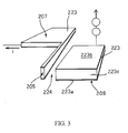
- Fig. 3 shows in detail vibrating microassembly 205 and electrode 209 of pressure sensor 201.
- Said vibrating microassembly 205, jointly with supporting base 207, and said electrode 209 are formed from a wafer 223 consisting of a first and a second silicon layer 223a, 223b, arranged parallel to each other, and of an intermediate layer 223c of silicon oxide (SOI wafer).
- SOI wafer silicon oxide
- Electrode 209 is formed from a portion of said first silicon layer 223a of said wafer 223.
- Vibrating microassembly 205 is formed near said portion of said first silicon layer 223a, and is made as a silicon beam arranged in a plane perpendicular to said first and second silicon layers 223a, 223b. It is formed by removing the surrounding portion of wafer 223, thereby creating a cavity 224 between microassembly 205 and electrode 209, within which cavity said microassembly can freely oscillate once excited.
- said microassembly 205 thanks to the electric field generated between it and electrode 209, vibrates in a direction parallel to said first and second silicon layers 223a, 223b and, ultimately, in a direction parallel to said electrode 209.
- Fig. 4 shows in detail vibrating microassembly 205 and electrode 209 of pressure sensor 201 according to a first variant embodiment.
- microassembly 205 vibrates in a direction perpendicular to said electrode 209.
- Said vibrating microassembly 205, jointly with supporting base 207, and said electrode 209 are formed from a wafer 225 consisting of a first and a second silicon layer 225a, 225b, arranged parallel to each other, and of an intermediate silicon oxide layer 225c (SOI wafer).
- Electrode 209 is formed from a portion of the first silicon layer 225a of said wafer 225, and vibrating microassembly 205 is formed from a corresponding portion of the second silicon layer 225b of said wafer 225, which portion is arranged above said electrode.
- Intermediate silicon oxide layer 225c in wafer 225 is correspondingly removed, so as to create a cavity 227 below microassembly 205, in order to allow said vibrating microassembly to freely oscillate.
- Both electrode 209 and microassembly 205 are equipped with contact areas 229 and 231, respectively, for connection to an electric circuit, more particularly an electric circuit like circuit 211 shown in Fig. 2.
- vibrating microassembly 205 is formed as a beam fastened at one end to supporting base 207.
- said beam is arranged in a plane parallel to said first and second silicon layers 225a, 225b, and it vibrates in a direction perpendicular to said first and second silicon layers 225a, 225b and, ultimately, in a direction perpendicular to said electrode 209.
- Fig. 5 shows in detail vibrating microassembly 205 and electrode 209 of pressure sensor 201 according to a second variant embodiment.
- microassembly 205 and electrode 209 are formed on two different wafers.
- Said vibrating microassembly 205 is formed from a wafer 233 consisting of a first and a second silicon layer 233a, 233b, arranged parallel to each other, and of an intermediate silicon oxide layer 233c (SOI wafer). More particularly, vibrating microassembly 205 is formed from a portion of second silicon layer 233b of said wafer 233. Intermediate layer 233c of silicon oxide of wafer 233 is correspondingly removed, so as to create a cavity 237 below microassembly 205, in order to allow said vibrating microassembly to freely oscillate.
- a wafer 233 consisting of a first and a second silicon layer 233a, 233b, arranged parallel to each other, and of an intermediate silicon oxide layer 233c (SOI wafer). More particularly, vibrating microassembly 205 is formed from a portion of second silicon layer 233b of said wafer 233. Intermediate layer 233c of silicon oxide of wafer 233 is correspondingly
- a Pyrex wafer 239 is coupled (by bonding) to SOI wafer 233, and more particularly to second silicon layer 233b in said wafer.
- the portion of said Pyrex wafer 239 located in correspondence with microassembly 205 is removed, so as to create a cavity 241 above said microassembly, in order to allow the latter to freely oscillate.
- vibrating microassembly 205 still formed as a beam, vibrates in a direction perpendicular to electrode 209.
- FIG. 6 there is shown a second embodiment of the pressure sensor according to the invention.
- pressure sensor 101 includes a microelectromechanical device 103 comprising a vibrating microassembly 105 fastened at one end 105a to a supporting base 107.
- Said vibrating microassembly 105 is preferably formed as a beam with a length in the range 200 to 800 micrometres, a width in the range 40 to 100 micrometres and a thickness in the range 1 to 50 micrometres,
- Supporting base 107 is joined, for instance by gluing, with a plate-shaped or disc-shaped piezoelectric element 109, allowing making microassembly 105 vibrate at known frequency and amplitude.
- piezoelectric element 109 is connected to a function generator (not shown), generating an electric signal for driving said piezoelectric element 109 at said known and constant frequency.
- said known and constant frequency is preferably the theoretical resonance frequency of the vibrating microassembly under absolute vacuum conditions (intrinsic frequency), but it might also be another frequency imposed by the function generator.
- the means for detecting the deviations of the oscillation frequency and/or amplitude of vibrating microassembly 105 due to pressure variations in the surrounding environment comprise an optical detection system 111.
- Said optical detection system 111 comprises a light source 113 directing an incoming light beam 115 onto the surface of said vibrating assembly 105, near free end 105b opposite to end 105a fastened to supporting base 107.
- Said light source 113 consists of a solid state laser diode 117 and a focussing lens 119 allowing focussing incoming beam 115 onto end 105b of vibrating microassembly 105.
- said laser diode 117 emits a radiation in the red spectral region, at a wavelength of about 670 nm.
- Optical detection system 111 further comprises a sensor 121 having a surface arranged to receive light beam 115' reflected by vibrating microassembly 105.
- sensor 121 is suitably associated with an electric circuit (not shown) providing an electric current value varying depending on the position of the point of incidence of said reflected beam 115' onto said surface 123.
- said electric circuit may further include a differential and transresistance amplifier in order to convert said electric current value into a voltage value varying depending on the position of the point of incidence of reflected beam 115' onto surface 123 of sensor 121.
- said electric circuit may further include, downstream said differential and transresistance amplifier, an amplifier equipped with a bandpass filter allowing passage of a very narrow frequency band centred about the resonance frequency of the vibration of the vibrating microassembly.
- reflected beam 115' will travel over paths of different lengths to impinge onto surface 123 of sensor 121. Due to the attenuation of beam 115', it might be possible to use, as an alternative to sensor 121, a sensor capable of supplying a current value varying depending on the intensity of said reflected beam 115', and not on the position of its point of incidence.
- Figs. 7 and 8 show the graphs of the oscillation frequency variation ( ⁇ f/f 0 ) and the quality factor (Q), respectively, as a function of the pressure in the environment surrounding sensor 101.
- Each graph includes different curves, corresponding to vibrating microassemblies made as beams with different sizes, more particularly (sizes in micrometres): Beam T1 T2 T3 T4 T5 T6 Length 800 200 400 400 600 800 Width 100 40 100 100 100 100 Thickness 5 5 10 5 5 10
- intrinsic frequency means the resonance frequency in the intrinsic pressure region (i.e., at pressure values lower than 10 -3 mbar), where the resonance frequency does not depend on the surrounding environment conditions; in other words, the intrinsic frequency may be intended as the resonance frequency expected under absolute vacuum conditions.
- the graph in Fig. 7 clearly shows the increment (in absolute value) of the frequency variation versus pressure in the pressure range between 1 and 10 3 mbar for all considered specimens.
- the pressure sensor according to the invention can be used with good reliability at pressures higher than 1 mbar.
- Fig. 7 clearly shows that the pressure sensor according to the invention attains the set aim, since it allows a direct measurement of the variation of the resonance frequency of the vibrating microassembly, said microassembly being allowed to freely vibrate at the frequency and amplitude set by the pressure in the surrounding environment, while keeping constant the value of the driving frequency of the control device as the pressure varies.
- the sensitivity of the pressure sensor according to the invention in terms of the slope of the frequency variation curve, increases as the microassembly thickness decreases, as it clearly appears from a comparison of the curves relating to specimens T3 and T4.
- said sensitivity increases as the microassembly surface area increases, as it clearly appears from a comparison of the curve relating to specimen T2 with the curves relating to specimens T1, T4 and T5.
- Fig. 8 there is shown the behaviour, as a function of pressure p (in millibars) of quality factor Q, defined as the ratio between the frequency value at the resonance peak and the half-height width of the resonance curve itself.
- the graph in Fig. 8 clearly shows the increment of quality factor Q as pressure decreases in the pressure range between 1 and 10 -3 mbar for almost all considered specimens. At pressures lower than 10 -3 mbar the above mentioned intrinsic region is entered and therefore no further increment in quality factor takes place.
- the pressure sensor according to the invention is utilisable with good reliability at pressures ranging from 10 3 to 10 -3 mbar.
- the sensitivity of the pressure sensor according to the invention increases as the microassembly thickness decreases, as it clearly appears from a comparison of the curves relating to specimens T1 and T6.
- said sensitivity increases as the microassembly surface area increases, as it clearly appears from a comparison of the curve relating to specimen T3 with the curves relating to specimens T1 and T5.
- the sensor according to the invention made according to any of the embodiments and the variants disclosed, attains the set aims: actually, since the detection of the variations of the oscillation frequency and/or amplitude of the vibrating microassembly is not a capacitive detection, it is possible to achieve a direct detection of the oscillation frequency and amplitude deviations from the expected values, due to pressure variations in the surrounding environment.
- the senor according to the invention can advantageously be utilised in several applications.
- the senor according to the invention in the field of vacuum pumps, and in particular vacuum pumps comprising a rotor and a stator co-operating together to obtain the pumping effect, thanks to its size, could be introduced into the vacuum pump and located between the stator and the rotor, without any difficulty depending on the size and without giving rise to significant perturbations.
Abstract
Description
- The present invention relates to a pressure sensor.
- More particularly, the present invention concerns a pressure sensor comprising a vibrating member, of which the oscillation frequency and amplitude are affected by the pressure conditions of the environment where the member is located, and can therefore be exploited to measure pressure variations in the surrounding environment.
- Pressure sensors, or sensors of other physical quantities such as temperature, density and so on, employing a vibrating member are already known. Said sensors exploit the influence of the pressure, temperature and/or density conditions of the external environment on the oscillation frequency and amplitude of said vibrating member, and allow calculating the variations of the physical quantity of interest by measuring the deviations of the oscillation frequency and amplitude from the expected values.
-
- In recent times, development of the technology of microelectromechanical devices (MEMs) has allowed manufacturing miniaturised sensors, consisting of a substrate onto which a single-layer or multilayer vibrating microassembly is formed. Said substrate and said vibrating microassembly are made, for instance, of silicon, silicon oxide, molybdenum, aluminium, etc.
- A microelectromechanical device is illustrated by way of example in Fig. 1.
- Said
microelectromechanical device 100 comprises a vibrating microassembly formed as aplanar membrane 102 suspended above acavity 104 formed in a supportingbase 106. Said supportingbase 106 is preferably a silicon substrate or wafer, wherecavity 104 is formed by conventional etching techniques. Saidmembrane 102 has a substantially rectangular shape and is fastened toperipheral rim 108 surroundingcavity 104 in supportingbase 106 at tworectangular fastening regions membrane 102. The membrane is further provided with aside extension 112 partly overlappingperipheral rim 108, so as to define acorresponding contact area 114. Ametal control electrode 118 is located insidecavity 104, in contact withbottom 116 thereof, and is provided with aside extension 120 bent againstside wall 122 ofcavity 104. That extension partly coversperipheral rim 108 of supportingbase 106 and defines acorresponding contact area 124. By applying a periodically modulated excitation voltage signal to saidareas control electrode 118 andmembrane 102, respectively, a variable electric field can be produced betweencontrol electrode 118 andmembrane 102, wherebymembrane 102 is made to vibrate. Under absolute vacuum conditions,membrane 102, suitably excited, will vibrate at the resonance frequency and amplitude corresponding to vacuum conditions (intrinsic frequency and amplitude), or, if said voltage signal is a sinusoidal signal whose frequencies are different from said resonance frequency, the membrane will vibrate at the frequency imposed by said signal. When departing from the ideal condition of absolute vacuum, the presence of gas molecules or atoms in the environment surrounding said membrane will affect the frequency and amplitude of the membrane oscillations, since the free vibration of the membrane will be perturbed by the collisions with said atoms and molecules. The higher the number of said atoms and molecules, hence the higher the pressure of the environment where the sensor is located, the stronger said influence. Consequently, by measuring the deviations of the frequency and/or amplitude of the vibration ofmembrane 102 from the expected values by means of a suitable detector, the pressure variations in the surrounding environment can be determined. Suitable materials formanufacturing membrane 102 may be aluminium, molybdenum, SiO2, Si3N4, Si (single crystalline). Moreover, membranes made of dielectric material, such as SiO2 and Si3N4, will have a sandwich structure (dielectric - metal - dielectric), with a metal layer sandwiched between two dielectric layers, so that the membrane vibration can be controlled by the electric field. - Miniaturised pressure sensors obtained by using microelectromechanical devices are disclosed, for instance, in
US 5,528,939 ,EP 1,026,491 andUS 6,532,822 . - Generally, in the prior art sensors, the microelectromechanical member is inserted into an electric circuit, and the variations of the oscillation amplitude and/or frequency of the vibrating microassembly related with pressure variation are detected from the variations of an electric parameter of said circuit.
- A drawback of the prior art devices is that the measurement of the variations of the oscillation frequency and/or amplitude of the vibrating microassembly is a capacitive measurement: this prevents a direct detection of the variations, and hence, a precise and accurate measurement,
- Actually, according to the prior art, the vibrating microassembly is placed between the plates of a capacitor belonging to said electric circuit or, possibly, the microassembly forms one of the plates of said capacitor, so that the variations in the frequency and/or amplitude of its oscillation entail capacitance variations. Yet, since measuring variations of a capacitance that is already variable per se because of the oscillatory motion of the vibrating microassembly would be an extremely complex operation, difficult to be performed in practice, a direct detection of the variations in the frequency and/or amplitude of said oscillatory motion is not performed. On the contrary, there is imposed the condition that the value of said capacitance keeps constant and equal to the theoretical value it would have if the vibrating microassembly would oscillate with the expected frequency and amplitude values, and there are measured the variations of the voltage signal exciting said vibrating microassembly, required to meet the aforementioned condition of constant capacitance.
- Thus, it is an object of the present invention to overcome the above limitation, by providing a pressure sensor comprising a vibrating microassembly, which sensor allows performing a direct detection of the deviations of the oscillation frequency and/or amplitude from the expected values, due to pressure variation in the surrounding environment.
- It is another object of the present invention to provide a pressure sensor that can be used with sufficient reliability within a wide range of pressure values.
- It is a further object of the present invention to provide a pressure sensor that exhibits a high detection sensitivity and repeatability.
- The above and other objects are achieved by the pressure sensor as claimed in the appended claims.
- Since the detection of the variations of the oscillation frequency and/or amplitude of the vibrating microassembly is not a capacitive detection, by using the sensor according to the invention said frequency and/or said amplitude can be allowed to freely vary, by driving the control device with a constant frequency signal, and the variations of said oscillation frequency and amplitude can be directly measured.
- In a preferred embodiment, thanks to the introduction of the vibrating microassembly into an electric circuit, the direct detection of the variations of the oscillation amplitude and/or frequency of the vibrating microassembly may be performed in simple and cheap manner by analysing the variations of an electric quantity in said electric circuit, in particular of a current.
- Advantageously, said electric circuit may be at least partly integrated onto the supporting base of the vibrating microassembly.
- In a second preferred embodiment, thanks to the use of a light source sending a light beam onto the surface of the vibrating microassembly, the direct measurement of the variations of the oscillation amplitude and/or frequency of the vibrating microassembly may be performed in simple and cheap manner by analysing the characteristics of the light beam reflected by said surface.
- Some preferred embodiments of the pressure sensor, given by way of non-limiting examples, will now be described in detail with reference to the accompanying drawings, in which:
- Fig. 1 is a perspective view of a microelectromechanical device (MEM) that can be employed in a pressure sensor;
- Fig. 2 schematically shows a first embodiment of the pressure sensor according to the invention;
- Fig. 3 is a schematic perspective view of the vibrating microassembly and the control device of the sensor shown in Fig. 2;
- Fig. 4 is a schematic cross-sectional view of the vibrating microassembly and the control device of the sensor shown in Fig. 2, according to a first variant;
- Fig. 5 is a schematic cross-sectional view of the vibrating microassembly and the control device of the sensor shown in Fig. 2, according to a second variant;
- Fig. 6 is schematic perspective view of a second embodiment of the pressure sensor according to the invention;
- Fig. 7 is a graph showing the behaviour of the oscillation frequency variation versus pressure in the pressure sensor shown in Fig. 6, for vibrating microassemblies with different sizes;
- Fig. 8 is a graph showing the behaviour of the quality factor versus pressure in the pressure sensor shown in Fig. 6, for vibrating microassemblies with different sizes.
- Referring to Fig. 2, there is shown a first embodiment of the pressure sensor according to the invention,
- According to said first embodiment,
pressure sensor 201 includes amicroelectromechanical device 203 consisting of a vibratingmicroassembly 205 fastened at oneend 205a to a supportingbase 207. - Said vibrating
microassembly 205 is preferably formed as a beam with a length in the range 200 to 800 micrometres, a width in the range 40 to 100 micrometres and a thickness in therange 1 to 50 micrometres, - Supporting
base 207 is joined with anelectrode 209 allowing makingmicroassembly 205 vibrate at known frequency and amplitude. - To this aim,
electrode 209 is connected to a voltage generator (not shown), generating an electric signal with said known frequency. - More particularly, according to the invention, said voltage generator drives
electrode 209 at constant frequency. - Said known and constant frequency is preferably the theoretical resonance frequency of the vibrating microassembly under absolute vacuum conditions (intrinsic frequency), but it might also be another frequency imposed by the voltage generator.
- According to this first embodiment of the invention, the means for detecting the deviations of the oscillation frequency and/or amplitude of vibrating
microassembly 205 related with pressure variation in the surrounding environment comprise anelectric circuit 211. - In
electric circuit 211, vibratingmicroassembly 205 is used as gate G of aMOSFET transistor 213. - As known, a MOSFET transistor, for instance of the N-channel type, comprises a low-doping P silicon substrate where two high-doping N regions (referred to as source S and drain D) are formed. A control electrode, the so-called gate G, is located between such regions. By varying the voltage applied to gate G, the charge distribution and density in the underlying substrate region between source S and drain D are varied by electric field effect, thereby creating a so-called channel. In the case described above, being the substrate of P type, the channel will be of N type, i.e. it will allow an electron current to flow. In case of N-type substrate, the channel created by the potential of gate G will allow a hole current to flow (P-type channel). Thus, the MOSFET is a device controlling current ID flowing therethrough, which current enters at a source S and flows out at a drain D, by a suitable biasing of the third pole, gate G. Should vibrating
microassembly 205 be used as gate G and said assembly be biased at a constant voltage VG, a resulting voltage signal will be the superposition of a constant d.c. signal and a frequency signal, since the gate channel extension will vary depending on the amplitude and frequency of the vibrating assembly oscillation. - Therefore, during the oscillations of the vibrating microassembly, current ID varies, in intensity and frequency, proportionally to the variations of the amplitude and frequency of said oscillations, and the measurement of the current variations allow directly obtaining the frequency and amplitude variations of the vibration of vibrating
microassembly 205, and consequently the pressure variations in the environment surrounding said assembly. - In the circuit shown in Fig. 2, drain D of said
MOSFET 213 of which vibratingmicroassembly 205 forms gate G, is connected to the drain of a second MOSFET 215 (parallel connection), identical to thefirst MOSFET 213 but having a non-variable gate. The sources of saidMOSFETs fourth MOSFETs fourth MOSFETs - Besides
MOSFETs electric circuit 211 preferably comprises anamplifier 221 amplifying the output signal in order to increase the sensitivity ofsensor 201. - It is to be appreciated that, advantageously,
electric circuit 211 may be at least partly integrated onto supportingbase 207, in order to further reduce the overall size ofsensor 201. More particularly, bothMOSFETs amplifier 221 may be integrated onto said supportingbase 207. - Fig. 3 shows in detail vibrating microassembly 205 and
electrode 209 ofpressure sensor 201. - Said vibrating microassembly 205, jointly with supporting
base 207, and saidelectrode 209 are formed from awafer 223 consisting of a first and asecond silicon layer intermediate layer 223c of silicon oxide (SOI wafer). -
Electrode 209 is formed from a portion of saidfirst silicon layer 223a of saidwafer 223. Vibrating microassembly 205 is formed near said portion of saidfirst silicon layer 223a, and is made as a silicon beam arranged in a plane perpendicular to said first andsecond silicon layers wafer 223, thereby creating acavity 224 betweenmicroassembly 205 andelectrode 209, within which cavity said microassembly can freely oscillate once excited. - Thus, said microassembly 205, thanks to the electric field generated between it and
electrode 209, vibrates in a direction parallel to said first andsecond silicon layers electrode 209. - Fig. 4 shows in detail vibrating microassembly 205 and
electrode 209 ofpressure sensor 201 according to a first variant embodiment. - Said variant embodiment differs from what has been shown and described with reference to Fig. 3 in that microassembly 205 vibrates in a direction perpendicular to said
electrode 209. - Said vibrating microassembly 205, jointly with supporting
base 207, and saidelectrode 209 are formed from awafer 225 consisting of a first and asecond silicon layer silicon oxide layer 225c (SOI wafer). -
Electrode 209 is formed from a portion of thefirst silicon layer 225a of saidwafer 225, and vibratingmicroassembly 205 is formed from a corresponding portion of thesecond silicon layer 225b of saidwafer 225, which portion is arranged above said electrode. Intermediatesilicon oxide layer 225c inwafer 225 is correspondingly removed, so as to create acavity 227 belowmicroassembly 205, in order to allow said vibrating microassembly to freely oscillate. - Both
electrode 209 and microassembly 205 are equipped withcontact areas circuit 211 shown in Fig. 2. - Also in this
variant vibrating microassembly 205 is formed as a beam fastened at one end to supportingbase 207. In the present case, however, said beam is arranged in a plane parallel to said first andsecond silicon layers second silicon layers electrode 209. - Fig. 5 shows in detail vibrating microassembly 205 and
electrode 209 ofpressure sensor 201 according to a second variant embodiment. - Said variant embodiment differs from what has been shown and described with reference to Fig. 4 in that
microassembly 205 andelectrode 209 are formed on two different wafers. - Said vibrating microassembly 205, jointly with supporting
base 207, is formed from awafer 233 consisting of a first and asecond silicon layer silicon oxide layer 233c (SOI wafer). More particularly, vibrating microassembly 205 is formed from a portion ofsecond silicon layer 233b of saidwafer 233.Intermediate layer 233c of silicon oxide ofwafer 233 is correspondingly removed, so as to create acavity 237 belowmicroassembly 205, in order to allow said vibrating microassembly to freely oscillate. - According to this variant, a
Pyrex wafer 239 is coupled (by bonding) toSOI wafer 233, and more particularly tosecond silicon layer 233b in said wafer. The portion of saidPyrex wafer 239 located in correspondence withmicroassembly 205 is removed, so as to create acavity 241 above said microassembly, in order to allow the latter to freely oscillate. -
Contact area 243 ofelectrode 209 for connection to an electric circuit, more particularly a circuit likecircuit 211 shown in Fig. 2, is provided inside saidcavity 241, more particularly in the wall above saidmicroassembly 205; asimilar contact area 245 is likewise applied to the face ofmicroassembly 205opposite electrode 209. - As in the variant shown in Fig. 4, also in this second variant vibrating microassembly 205, still formed as a beam, vibrates in a direction perpendicular to
electrode 209. - Referring to Fig. 6, there is shown a second embodiment of the pressure sensor according to the invention,
- According to said second embodiment,
pressure sensor 101 includes amicroelectromechanical device 103 comprising a vibrating microassembly 105 fastened at oneend 105a to a supportingbase 107. - Said vibrating microassembly 105 is preferably formed as a beam with a length in the range 200 to 800 micrometres, a width in the range 40 to 100 micrometres and a thickness in the
range 1 to 50 micrometres, - Supporting
base 107 is joined, for instance by gluing, with a plate-shaped or disc-shapedpiezoelectric element 109, allowing making microassembly 105 vibrate at known frequency and amplitude. - To this aim,
piezoelectric element 109 is connected to a function generator (not shown), generating an electric signal for driving saidpiezoelectric element 109 at said known and constant frequency. - More particularly, said known and constant frequency is preferably the theoretical resonance frequency of the vibrating microassembly under absolute vacuum conditions (intrinsic frequency), but it might also be another frequency imposed by the function generator.
- According to this second embodiment of the invention, the means for detecting the deviations of the oscillation frequency and/or amplitude of vibrating microassembly 105 due to pressure variations in the surrounding environment, comprise an
optical detection system 111. - Said
optical detection system 111 comprises alight source 113 directing anincoming light beam 115 onto the surface of said vibratingassembly 105, nearfree end 105b opposite to end 105a fastened to supportingbase 107. Saidlight source 113 consists of a solidstate laser diode 117 and a focussinglens 119 allowing focussingincoming beam 115 ontoend 105b of vibratingmicroassembly 105. - Preferably, said
laser diode 117 emits a radiation in the red spectral region, at a wavelength of about 670 nm. -
Optical detection system 111 further comprises asensor 121 having a surface arranged to receive light beam 115' reflected by vibratingmicroassembly 105. - It is clear that, as the oscillation frequency and/or amplitude of said vibrating microassembly 105 change, the position of the point of incidence of reflected beam 115' on
surface 123 ofsensor 121 will change. In order to detect such variations of the oscillation frequency and/or amplitude,sensor 121 is suitably associated with an electric circuit (not shown) providing an electric current value varying depending on the position of the point of incidence of said reflected beam 115' onto saidsurface 123. - Advantageously, said electric circuit may further include a differential and transresistance amplifier in order to convert said electric current value into a voltage value varying depending on the position of the point of incidence of reflected beam 115' onto
surface 123 ofsensor 121. - Also, said electric circuit may further include, downstream said differential and transresistance amplifier, an amplifier equipped with a bandpass filter allowing passage of a very narrow frequency band centred about the resonance frequency of the vibration of the vibrating microassembly.
- It is to be appreciated that, due to the variations of the oscillation amplitude and/or frequency of vibrating microassembly 105, reflected beam 115' will travel over paths of different lengths to impinge onto
surface 123 ofsensor 121. Due to the attenuation of beam 115', it might be possible to use, as an alternative tosensor 121, a sensor capable of supplying a current value varying depending on the intensity of said reflected beam 115', and not on the position of its point of incidence. - Figs. 7 and 8 show the graphs of the oscillation frequency variation (Δf/f0) and the quality factor (Q), respectively, as a function of the pressure in the
environment surrounding sensor 101. - Each graph includes different curves, corresponding to vibrating microassemblies made as beams with different sizes, more particularly (sizes in micrometres):
Beam T1 T2 T3 T4 T5 T6 Length 800 200 400 400 600 800 Width 100 40 100 100 100 100 Thickness 5 5 10 5 5 10 - Referring to Fig. 7, there is shown the behaviour, as a function of pressure p (in millibars), of the frequency variation, defined as:

where f(p) is the resonance frequency at pressure p
f0 is the intrinsic frequency. - Note that "intrinsic frequency" means the resonance frequency in the intrinsic pressure region (i.e., at pressure values lower than 10-3 mbar), where the resonance frequency does not depend on the surrounding environment conditions; in other words, the intrinsic frequency may be intended as the resonance frequency expected under absolute vacuum conditions.
- The graph in Fig. 7 clearly shows the increment (in absolute value) of the frequency variation versus pressure in the pressure range between 1 and 103 mbar for all considered specimens.
- At pressures of the order of or lower than 1 mbar, on the contrary, f(p) ≅ f0, and hence Δf quickly tends to 0.
- Thus, by relying on the measurement of the resonance frequency variation only, the pressure sensor according to the invention can be used with good reliability at pressures higher than 1 mbar.
- It is to be appreciated that Fig. 7 clearly shows that the pressure sensor according to the invention attains the set aim, since it allows a direct measurement of the variation of the resonance frequency of the vibrating microassembly, said microassembly being allowed to freely vibrate at the frequency and amplitude set by the pressure in the surrounding environment, while keeping constant the value of the driving frequency of the control device as the pressure varies.
- Also, by analysing the curves of the graph shown in Fig. 7, it is possible to appreciate that the sensitivity of the pressure sensor according to the invention, in terms of the slope of the frequency variation curve, increases as the microassembly thickness decreases, as it clearly appears from a comparison of the curves relating to specimens T3 and T4. Moreover, at constant thickness, said sensitivity increases as the microassembly surface area increases, as it clearly appears from a comparison of the curve relating to specimen T2 with the curves relating to specimens T1, T4 and T5.
- Turning now to Fig. 8, there is shown the behaviour, as a function of pressure p (in millibars) of quality factor Q, defined as the ratio between the frequency value at the resonance peak and the half-height width of the resonance curve itself.
- The graph in Fig. 8 clearly shows the increment of quality factor Q as pressure decreases in the pressure range between 1 and 10-3 mbar for almost all considered specimens. At pressures lower than 10-3 mbar the above mentioned intrinsic region is entered and therefore no further increment in quality factor takes place.
- Thus, by virtue of the combined measurement of the resonance frequency variation and the quality factor variation, the pressure sensor according to the invention is utilisable with good reliability at pressures ranging from 103 to 10-3 mbar.
- By analysing the curves of the graph shown in Fig. 8, it is possible to appreciate that the sensitivity of the pressure sensor according to the invention, also in terms of the slope of the quality factor curve, increases as the microassembly thickness decreases, as it clearly appears from a comparison of the curves relating to specimens T1 and T6. Moreover, at constant thickness, said sensitivity increases as the microassembly surface area increases, as it clearly appears from a comparison of the curve relating to specimen T3 with the curves relating to specimens T1 and T5.
- It is clear that the sensor according to the invention, made according to any of the embodiments and the variants disclosed, attains the set aims: actually, since the detection of the variations of the oscillation frequency and/or amplitude of the vibrating microassembly is not a capacitive detection, it is possible to achieve a direct detection of the oscillation frequency and amplitude deviations from the expected values, due to pressure variations in the surrounding environment.
- It is also clear that, thanks to the very reduced size, the satisfactory sensitivity and the possibility of operating in a wide pressure range (103 to 10-3 mbar), the sensor according to the invention can advantageously be utilised in several applications.
- By way of non-limiting example, in the field of vacuum pumps, and in particular vacuum pumps comprising a rotor and a stator co-operating together to obtain the pumping effect, the sensor according to the invention, thanks to its size, could be introduced into the vacuum pump and located between the stator and the rotor, without any difficulty depending on the size and without giving rise to significant perturbations.
Claims (34)
- A pressure sensor (201) comprising:- a vibrating microassembly (205) fastened to a supporting base (207);- a control device (209) for said microassembly, to make it oscillate relative to said supporting base at a known frequency and amplitude; and- means (211) for detecting the deviations of the frequency and/or amplitude of said oscillation of said microassembly from said known frequency and/or amplitude,
said control device (209) being driven by a constant frequency signal, characterised in that said means for detecting said frequency and/or amplitude deviations include an electric circuit (211) in which at least one electric parameter is variable depending on the oscillation amplitude and/or frequency of said vibrating microassembly (205). - A pressure sensor (201) as claimed in claim 1, wherein said electric parameter is a current.
- A pressure sensor (201) as claimed in claim 1 or 2, wherein said electric circuit includes a MOSFET transistor (213), said vibrating microassembly acting as control electrode or gate (G) of said MOSFET transistor.
- A pressure sensor (201) as claimed in claim 3, wherein said gate (G) is fed with a constant voltage.
- A pressure sensor (201) as claimed in claim 3, wherein said MOSFET transistor (213) comprising said vibrating assembly (205) as its gate is connected in parallel with a second MOSFET transistor (215).
- A pressure sensor (201) as claimed in claim 5, wherein said second MOSFET transistor (215) is identical to said first MOSFET transistor (213), except that it has a stationary gate.
- A pressure sensor (201) as claimed in claim 5 or 6, wherein said first and second MOSFET transistors (213, 215) are connected in series with a third and a fourth MOSFET transistor (217, 219), respectively, said third and fourth MOSFET transistors acting so as to make said circuit more stable.
- A pressure sensor (201) as claimed in claim 7, wherein said third and fourth MOSFET transistors (217, 219) are identical.
- A pressure sensor (201) as claimed in any of claims 1 to 8, wherein said electric circuit further comprises an amplifier for amplifying the variations of said electric parameter.
- A pressure sensor (201) as claimed in any of claims 1 to 9, wherein said electric circuit (211) is at least partly integrated onto said supporting base (207) of said vibrating microassembly (205).
- A pressure sensor (201) as claimed in claim 1, wherein said control device is a control electrode (209).
- A pressure sensor (201) as claimed in claim 11, wherein said vibrating microassembly (205) oscillates in a direction parallel to said control electrode (209).
- A pressure sensor (201) as claimed in claim 12, wherein said sensor comprises a wafer (223) consisting of a first and a second silicon layer (223a, 223b), arranged parallel to each other, and of an intermediate layer (223c) of silicon oxide, wherein said control electrode (209) is formed from a portion of said first silicon layer (223a), and wherein said vibrating microassembly (205) is formed near said portion of said first silicon layer (223a) as a silicon beam arranged in a plane perpendicular to said first and second silicon layers (223a, 223b), the surrounding portion of said wafer (223) being removed to create a cavity (224) between said microassembly (205) and said electrode (209), in order to allow said microassembly to freely oscillate.
- A pressure sensor (201) as claimed in claim 11, wherein said vibrating microassembly (205) oscillates in a direction perpendicular to said control electrode (209).
- A pressure sensor (201) as claimed in claim 14, wherein said sensor comprises a wafer (225) consisting of a first and a second silicon layer (225a, 225b), arranged parallel to each other, and of an intermediate layer (225c) of silicon oxide, wherein said control electrode (209) is formed from a portion of said first silicon layer (225a), and wherein said vibrating microassembly (205) is formed from a portion of said second silicon layer (225b) facing said portion of said first layer, the intermediate silicon oxide layer (225c) being correspondingly removed to create a cavity (227) below said vibrating microassembly (205) in order to allow said vibrating microassembly to freely oscillate.
- A pressure sensor (201) as claimed in claim 14, wherein said sensor comprises: a first wafer (233) consisting of a first and a second silicon layer (233a, 233b), arranged parallel to each other, and of an intermediate layer (233c) of silicon oxide, said vibrating microassembly (205) being formed from a portion of said second silicon layer (233) of said first wafer, the intermediate silicon oxide layer (233c) being correspondingly removed to create a cavity (237) below said vibrating microassembly (205); and a second wafer (239), made of Pyrex, superimposed to said second silicon layer (233b) in said fist wafer (233), a cavity (241) being formed in said second wafer (239), in correspondence with said vibrating microassembly (205), in order to allow said vibrating microassembly to freely oscillate, said control electrode (209) being located inside said cavity (241) of said second wafer (239).
- A pressure sensor (101) comprising:- a vibrating microassembly (105) fastened to a supporting base (107);- a control device (109) for said microassembly, to make it oscillate relative to said supporting base at a known frequency and amplitude; and- means (111) for detecting the deviations of the frequency and/or amplitude of said oscillation of said microassembly from said known frequency and/or amplitude,said control device (109) being driven by a constant frequency signal, characterised in that said means for detecting said frequency and/or amplitude deviations include an optical detection system (111).
- A pressure sensor (101) as claimed in claim 17, wherein said optical detection system (111) includes a light source (113) for directing an incoming light beam (115) onto the surface of said vibrating microassembly (105).
- A pressure sensor (101) as claimed in claim 18, wherein said light source comprises a solid state laser diode (117).
- A pressure sensor (101) as claimed in claim 18, wherein said laser diode (117) emits at a wavelength of about 670 nm.
- A pressure sensor (101) as claimed in claim 18, wherein said optical detection system (111) further comprises a sensor (121) having a surface (123) arranged to receive the light beam (115') reflected by said vibrating microassembly (105), and at least one electric contact providing a current value varying depending on the position of the point of incidence of said reflected beam (115') onto said surface (123).
- A pressure sensor (101) as claimed in claim 18, wherein said optical detection system (111) further includes a sensor (121) having a surface (123) arranged to receive the light beam (115') reflected by said vibrating microassembly (105), and at least one electric contact providing a current value varying depending on the intensity of said reflected beam (115') when impinging onto said surface (123).
- A pressure sensor (101) as claimed in claim 21 or 22, wherein said sensor further includes a differential and transresistance amplifier to convert said current value into a variable voltage value.
- A pressure sensor (101) as claimed in claim 23, wherein said sensor further includes, downstream said differential and transresistance amplifier, an amplifier equipped with a bandpass filter allowing the passage of a very narrow frequency band centred about the vibration resonance frequency of said vibrating microassembly.
- A pressure sensor (101) as claimed in claim 17, wherein said control device includes a piezoelectric element (109).
- A pressure sensor (101) as claimed in claim 25, wherein said piezoelectric element (109) is plate-shaped or disc-shaped.
- A pressure sensor (101) as claimed in claim 25 or 26, wherein said piezoelectric element (109) is joined to said supporting base (107) of said vibrating microassembly (105), for instance by gluing.
- A pressure sensor (101) as claimed in claim 25, wherein said control device (109) further includes a function generator for generating said electric signal for driving said piezoelectric element at a constant frequency.
- A pressure sensor (101) as claimed in any of claims 17 to 28, wherein said vibrating microassembly (105) is formed as a beam having a length in the range 200 to 800 micrometres, a width in the range 40 to 100 micrometres and a thickness in the range 1 to 50 micrometres.
- A pressure sensor (101) as claimed in any of claims 17 to 29, wherein the frequency of the signal driving said control device (109) is equal to the intrinsic frequency of said vibrating microassembly (105).
- A method of pressure detection, comprising the following steps:- providing a vibrating microassembly (105) fastened to a supporting base (107);- providing a control device (109) for making said microassembly oscillate relative to said supporting base at known frequency and amplitude, said control device being driven by a constant frequency signal;- providing a light source (113) to generate a light beam (115);- directing said light beam onto the surface of said vibrating microassembly;- providing a sensor (121) having a surface arranged to receive the light beam reflected by said vibrating microassembly, and at least one electric contact providing a value of an electric quantity varying depending on the position of the point of incidence and/or on the intensity of said reflected beam at said surface;- measuring the variations of said electric quantity to obtain the frequency and/or amplitude variations of said vibrating microassembly.
- A method of pressure detection as claimed in claim 31, further comprising a step of amplifying the variations of said electric quantity before measuring said variations.
- A method of pressure detection as claimed in claim 31 or 32, wherein said electric quantity is an electric current.
- A method of pressure detection as claimed in claim 31 or 32, wherein said electric quantity is an electric voltage.
Applications Claiming Priority (1)
| Application Number | Priority Date | Filing Date | Title |
|---|---|---|---|
| IT000316A ITTO20050316A1 (en) | 2005-05-10 | 2005-05-10 | PRESSURE SENSOR |
Publications (2)
| Publication Number | Publication Date |
|---|---|
| EP1722210A2 true EP1722210A2 (en) | 2006-11-15 |
| EP1722210A3 EP1722210A3 (en) | 2010-01-27 |
Family
ID=36615724
Family Applications (1)
| Application Number | Title | Priority Date | Filing Date |
|---|---|---|---|
| EP06113734A Withdrawn EP1722210A3 (en) | 2005-05-10 | 2006-05-09 | Pressure sensor with a vibrating member |
Country Status (4)
| Country | Link |
|---|---|
| US (1) | US7334481B2 (en) |
| EP (1) | EP1722210A3 (en) |
| JP (1) | JP2006322935A (en) |
| IT (1) | ITTO20050316A1 (en) |
Cited By (2)
| Publication number | Priority date | Publication date | Assignee | Title |
|---|---|---|---|---|
| US8256298B2 (en) | 2009-10-07 | 2012-09-04 | Nxp B.V. | MEMS pressure sensor |
| CN104339624A (en) * | 2014-10-23 | 2015-02-11 | 金都精密机械(大连)有限公司 | Profile extrusion setting table vacuum system and working method thereof |
Families Citing this family (6)
| Publication number | Priority date | Publication date | Assignee | Title |
|---|---|---|---|---|
| FR2888930B1 (en) * | 2004-12-27 | 2007-08-31 | Thales Sa | RESONATOR MEASURING DEVICE AND METHOD USING THE DEVICE |
| US7745296B2 (en) * | 2005-06-08 | 2010-06-29 | Globalfoundries Inc. | Raised source and drain process with disposable spacers |
| WO2010022038A2 (en) * | 2008-08-19 | 2010-02-25 | University Of Florida Research Foundation, Inc. | Pressure sensing |
| WO2012140846A1 (en) * | 2011-04-12 | 2012-10-18 | パナソニック株式会社 | Mems pressure sensor |
| GB2509105B (en) * | 2012-12-20 | 2017-02-22 | Oxsensis Ltd | Mechanical resonator sensor |
| DE102017215849B4 (en) * | 2017-09-08 | 2019-07-18 | Continental Automotive Gmbh | Method for checking the function of a pressure sensor in the air intake tract or exhaust gas outlet tract of an internal combustion engine in operation and engine control unit |
Citations (7)
| Publication number | Priority date | Publication date | Assignee | Title |
|---|---|---|---|---|
| US4841775A (en) | 1985-09-06 | 1989-06-27 | Yokogawa Electric Corporation | Vibratory transducer |
| EP0435553A2 (en) | 1989-12-29 | 1991-07-03 | Solartron Group Limited | Optical sensing systems |
| EP0505177A1 (en) | 1991-03-19 | 1992-09-23 | Lucas Industries Public Limited Company | Vibrating sensor |
| US5528939A (en) | 1995-03-21 | 1996-06-25 | Martin; Jacob H. | Micromechanical pressure gauge having extended sensor range |
| EP1026491A2 (en) | 1994-12-16 | 2000-08-09 | Honeywell Inc. | Integrated resonant microbeam sensor and transistor oscillator |
| US6532822B1 (en) | 2000-09-26 | 2003-03-18 | Clark Davis Boyd | Resonant torsion pendulum pressure sensor |
| EP1530036A1 (en) | 2003-11-07 | 2005-05-11 | VARIAN S.p.A. | Pressure sensor |
Family Cites Families (8)
| Publication number | Priority date | Publication date | Assignee | Title |
|---|---|---|---|---|
| SE414672B (en) * | 1978-11-16 | 1980-08-11 | Asea Ab | FIBEROPTICAL DON FOR Saturation of Physical Properties such as Force, Tensile, Pressure, Acceleration and Temperature |
| GB8701556D0 (en) * | 1987-01-24 | 1987-02-25 | Schlumberger Electronics Uk | Sensors |
| JP2641104B2 (en) * | 1989-01-10 | 1997-08-13 | 本田技研工業株式会社 | Semiconductor stress sensor |
| US5195374A (en) * | 1989-08-30 | 1993-03-23 | Schlumberger Industries Limited | Sensor systems |
| DE4031369A1 (en) * | 1990-10-04 | 1992-04-09 | Bosch Gmbh Robert | SENSOR |
| WO1995002173A1 (en) * | 1993-07-06 | 1995-01-19 | Seiko Epson Corporation | Method and device for measuring pressure using crystal resonator |
| US6085594A (en) * | 1998-09-04 | 2000-07-11 | The United States Of America As Represented By The Administrator Of The National Aeronautics And Space Administration | High resolution and large dynamic range resonant pressure sensor based on Q-factor measurement |
| JP4082907B2 (en) * | 2002-01-21 | 2008-04-30 | 正喜 江刺 | Vibration type pressure sensor |
-
2005
- 2005-05-10 IT IT000316A patent/ITTO20050316A1/en unknown
-
2006
- 2006-05-09 EP EP06113734A patent/EP1722210A3/en not_active Withdrawn
- 2006-05-09 US US11/430,403 patent/US7334481B2/en not_active Expired - Fee Related
- 2006-05-09 JP JP2006130489A patent/JP2006322935A/en not_active Withdrawn
Patent Citations (8)
| Publication number | Priority date | Publication date | Assignee | Title |
|---|---|---|---|---|
| US4841775A (en) | 1985-09-06 | 1989-06-27 | Yokogawa Electric Corporation | Vibratory transducer |
| EP0435553A2 (en) | 1989-12-29 | 1991-07-03 | Solartron Group Limited | Optical sensing systems |
| EP0505177A1 (en) | 1991-03-19 | 1992-09-23 | Lucas Industries Public Limited Company | Vibrating sensor |
| EP1026491A2 (en) | 1994-12-16 | 2000-08-09 | Honeywell Inc. | Integrated resonant microbeam sensor and transistor oscillator |
| EP1132728A2 (en) | 1994-12-16 | 2001-09-12 | Honeywell Inc. | Integrated resonant microbeam sensor and transistor oscillator |
| US5528939A (en) | 1995-03-21 | 1996-06-25 | Martin; Jacob H. | Micromechanical pressure gauge having extended sensor range |
| US6532822B1 (en) | 2000-09-26 | 2003-03-18 | Clark Davis Boyd | Resonant torsion pendulum pressure sensor |
| EP1530036A1 (en) | 2003-11-07 | 2005-05-11 | VARIAN S.p.A. | Pressure sensor |
Cited By (2)
| Publication number | Priority date | Publication date | Assignee | Title |
|---|---|---|---|---|
| US8256298B2 (en) | 2009-10-07 | 2012-09-04 | Nxp B.V. | MEMS pressure sensor |
| CN104339624A (en) * | 2014-10-23 | 2015-02-11 | 金都精密机械(大连)有限公司 | Profile extrusion setting table vacuum system and working method thereof |
Also Published As
| Publication number | Publication date |
|---|---|
| JP2006322935A (en) | 2006-11-30 |
| EP1722210A3 (en) | 2010-01-27 |
| US20060266124A1 (en) | 2006-11-30 |
| US7334481B2 (en) | 2008-02-26 |
| ITTO20050316A1 (en) | 2006-11-11 |
Similar Documents
| Publication | Publication Date | Title |
|---|---|---|
| EP1722210A2 (en) | Pressure sensor with a vibrating member | |
| US4841775A (en) | Vibratory transducer | |
| US20110107838A1 (en) | Mems pressure sensor | |
| JP3102320B2 (en) | Sensor device | |
| US20070074574A1 (en) | Micro-electro-mechanical pressure sensor | |
| JPH11271207A (en) | Sensor, particularly, sensor for measuring viscosity and density of medium | |
| EP1471340B1 (en) | Vibrating type pressure sensor | |
| US20220136957A1 (en) | Photoacoustic spectroscope having a vibrating structure as sound detector | |
| JP2002501620A (en) | Microsensor with resonator structure | |
| US5969257A (en) | Pressure measuring membrane with resonant element vibrating orthogonal to membrane movement | |
| CN114286935A (en) | MEMS-based photoacoustic cell | |
| EP1034415A1 (en) | Dynamic pressure sensor, photo acoustic gas detector, microphone, hydrophone and their manufacturing | |
| JPH0643179A (en) | Acceleration sensor and manufacture of said sensor | |
| EP1530036B1 (en) | Pressure sensor | |
| US20230048120A1 (en) | Resonant sensor using mems resonator, and detection method by resonant sensor | |
| Brand et al. | Ultrasound barrier microsystem for object detection based on micromachined transducer elements | |
| GB2297618A (en) | Angular velocity sensor and manufacturing process | |
| JPH0783756A (en) | Oscillatory type infrared sensor, oscillatory type infrared imager, and infrared-ray detecting method | |
| Beeby et al. | Thick-film PZT-silicon micromechanical resonator | |
| Hornung et al. | Micromachined ultrasound-based Proximity sensors | |
| US11757408B2 (en) | Electric field detector | |
| JPH11201788A (en) | Semi-conductor karman vortex flow rate sensor, and its manufacture | |
| JPH05203517A (en) | Sensor device | |
| JPH06268237A (en) | Semiconductor acceleration sensor | |
| JP2797742B2 (en) | Vibration transducer |
Legal Events
| Date | Code | Title | Description |
|---|---|---|---|
| PUAI | Public reference made under article 153(3) epc to a published international application that has entered the european phase |
Free format text: ORIGINAL CODE: 0009012 |
|
| AK | Designated contracting states |
Kind code of ref document: A2 Designated state(s): AT BE BG CH CY CZ DE DK EE ES FI FR GB GR HU IE IS IT LI LT LU LV MC NL PL PT RO SE SI SK TR |
|
| AX | Request for extension of the european patent |
Extension state: AL BA HR MK YU |
|
| PUAL | Search report despatched |
Free format text: ORIGINAL CODE: 0009013 |
|
| AK | Designated contracting states |
Kind code of ref document: A3 Designated state(s): AT BE BG CH CY CZ DE DK EE ES FI FR GB GR HU IE IS IT LI LT LU LV MC NL PL PT RO SE SI SK TR |
|
| AX | Request for extension of the european patent |
Extension state: AL BA HR MK YU |
|
| 17P | Request for examination filed |
Effective date: 20100719 |
|
| AKX | Designation fees paid |
Designated state(s): DE FR GB |
|
| RAP1 | Party data changed (applicant data changed or rights of an application transferred) |
Owner name: AGILENT TECHNOLOGIES ITALIA S.P.A. |
|
| RAP1 | Party data changed (applicant data changed or rights of an application transferred) |
Owner name: AGILENT TECHNOLOGIES ITALIA S.P.A. |
|
| RAP1 | Party data changed (applicant data changed or rights of an application transferred) |
Owner name: AGILENT TECHNOLOGIES, INC. |
|
| 17Q | First examination report despatched |
Effective date: 20121211 |
|
| STAA | Information on the status of an ep patent application or granted ep patent |
Free format text: STATUS: THE APPLICATION IS DEEMED TO BE WITHDRAWN |
|
| 18D | Application deemed to be withdrawn |
Effective date: 20130423 |