EP1026491A2 - Integrated resonant microbeam sensor and transistor oscillator - Google Patents
Integrated resonant microbeam sensor and transistor oscillator Download PDFInfo
- Publication number
- EP1026491A2 EP1026491A2 EP00201303A EP00201303A EP1026491A2 EP 1026491 A2 EP1026491 A2 EP 1026491A2 EP 00201303 A EP00201303 A EP 00201303A EP 00201303 A EP00201303 A EP 00201303A EP 1026491 A2 EP1026491 A2 EP 1026491A2
- Authority
- EP
- European Patent Office
- Prior art keywords
- transistor
- electrode
- terminal
- terminal connected
- microbeam
- Prior art date
- Legal status (The legal status is an assumption and is not a legal conclusion. Google has not performed a legal analysis and makes no representation as to the accuracy of the status listed.)
- Withdrawn
Links
- 239000000758 substrate Substances 0.000 claims abstract description 32
- 239000003990 capacitor Substances 0.000 claims abstract description 19
- 238000005452 bending Methods 0.000 claims abstract description 7
- 230000001419 dependent effect Effects 0.000 claims abstract description 6
- 230000005669 field effect Effects 0.000 claims description 7
- 230000008878 coupling Effects 0.000 claims description 5
- 238000010168 coupling process Methods 0.000 claims description 5
- 238000005859 coupling reaction Methods 0.000 claims description 5
- 230000006835 compression Effects 0.000 claims 9
- 238000007906 compression Methods 0.000 claims 9
- XUIMIQQOPSSXEZ-UHFFFAOYSA-N Silicon Chemical compound [Si] XUIMIQQOPSSXEZ-UHFFFAOYSA-N 0.000 description 8
- 238000000034 method Methods 0.000 description 8
- 229910052710 silicon Inorganic materials 0.000 description 8
- 239000010703 silicon Substances 0.000 description 8
- 230000008901 benefit Effects 0.000 description 7
- 229910021420 polycrystalline silicon Inorganic materials 0.000 description 7
- 229920005591 polysilicon Polymers 0.000 description 7
- 230000008569 process Effects 0.000 description 7
- 230000008859 change Effects 0.000 description 6
- 230000009977 dual effect Effects 0.000 description 6
- 238000004458 analytical method Methods 0.000 description 5
- 238000013459 approach Methods 0.000 description 5
- 238000006073 displacement reaction Methods 0.000 description 5
- 230000010355 oscillation Effects 0.000 description 5
- 238000004519 manufacturing process Methods 0.000 description 4
- 230000001133 acceleration Effects 0.000 description 3
- 238000006243 chemical reaction Methods 0.000 description 3
- 238000013461 design Methods 0.000 description 3
- 238000010586 diagram Methods 0.000 description 3
- 238000005516 engineering process Methods 0.000 description 3
- 229910044991 metal oxide Inorganic materials 0.000 description 3
- 150000004706 metal oxides Chemical class 0.000 description 3
- 239000004065 semiconductor Substances 0.000 description 3
- 230000003247 decreasing effect Effects 0.000 description 2
- 230000007774 longterm Effects 0.000 description 2
- 239000000463 material Substances 0.000 description 2
- 238000005259 measurement Methods 0.000 description 2
- 150000004767 nitrides Chemical class 0.000 description 2
- 230000010363 phase shift Effects 0.000 description 2
- 230000035945 sensitivity Effects 0.000 description 2
- 230000009471 action Effects 0.000 description 1
- 230000003321 amplification Effects 0.000 description 1
- 230000003190 augmentative effect Effects 0.000 description 1
- 230000015572 biosynthetic process Effects 0.000 description 1
- 230000000295 complement effect Effects 0.000 description 1
- 239000013078 crystal Substances 0.000 description 1
- 238000013016 damping Methods 0.000 description 1
- 238000009795 derivation Methods 0.000 description 1
- 238000009792 diffusion process Methods 0.000 description 1
- 230000000694 effects Effects 0.000 description 1
- 230000007613 environmental effect Effects 0.000 description 1
- 238000010438 heat treatment Methods 0.000 description 1
- 239000007943 implant Substances 0.000 description 1
- 238000002955 isolation Methods 0.000 description 1
- 238000005459 micromachining Methods 0.000 description 1
- 238000003199 nucleic acid amplification method Methods 0.000 description 1
- 238000012545 processing Methods 0.000 description 1
- 239000010453 quartz Substances 0.000 description 1
- 238000009877 rendering Methods 0.000 description 1
- 238000007789 sealing Methods 0.000 description 1
- VYPSYNLAJGMNEJ-UHFFFAOYSA-N silicon dioxide Inorganic materials O=[Si]=O VYPSYNLAJGMNEJ-UHFFFAOYSA-N 0.000 description 1
- 230000006641 stabilisation Effects 0.000 description 1
- 238000011105 stabilization Methods 0.000 description 1
Images






Classifications
-
- G—PHYSICS
- G01—MEASURING; TESTING
- G01P—MEASURING LINEAR OR ANGULAR SPEED, ACCELERATION, DECELERATION, OR SHOCK; INDICATING PRESENCE, ABSENCE, OR DIRECTION, OF MOVEMENT
- G01P15/00—Measuring acceleration; Measuring deceleration; Measuring shock, i.e. sudden change of acceleration
- G01P15/02—Measuring acceleration; Measuring deceleration; Measuring shock, i.e. sudden change of acceleration by making use of inertia forces using solid seismic masses
- G01P15/08—Measuring acceleration; Measuring deceleration; Measuring shock, i.e. sudden change of acceleration by making use of inertia forces using solid seismic masses with conversion into electric or magnetic values
- G01P15/097—Measuring acceleration; Measuring deceleration; Measuring shock, i.e. sudden change of acceleration by making use of inertia forces using solid seismic masses with conversion into electric or magnetic values by vibratory elements
-
- G—PHYSICS
- G01—MEASURING; TESTING
- G01L—MEASURING FORCE, STRESS, TORQUE, WORK, MECHANICAL POWER, MECHANICAL EFFICIENCY, OR FLUID PRESSURE
- G01L1/00—Measuring force or stress, in general
- G01L1/18—Measuring force or stress, in general using properties of piezo-resistive materials, i.e. materials of which the ohmic resistance varies according to changes in magnitude or direction of force applied to the material
- G01L1/183—Measuring force or stress, in general using properties of piezo-resistive materials, i.e. materials of which the ohmic resistance varies according to changes in magnitude or direction of force applied to the material by measuring variations of frequency of vibrating piezo-resistive material
-
- G—PHYSICS
- G01—MEASURING; TESTING
- G01L—MEASURING FORCE, STRESS, TORQUE, WORK, MECHANICAL POWER, MECHANICAL EFFICIENCY, OR FLUID PRESSURE
- G01L9/00—Measuring steady of quasi-steady pressure of fluid or fluent solid material by electric or magnetic pressure-sensitive elements; Transmitting or indicating the displacement of mechanical pressure-sensitive elements, used to measure the steady or quasi-steady pressure of a fluid or fluent solid material, by electric or magnetic means
- G01L9/0001—Transmitting or indicating the displacement of elastically deformable gauges by electric, electro-mechanical, magnetic or electro-magnetic means
- G01L9/0008—Transmitting or indicating the displacement of elastically deformable gauges by electric, electro-mechanical, magnetic or electro-magnetic means using vibrations
- G01L9/0019—Transmitting or indicating the displacement of elastically deformable gauges by electric, electro-mechanical, magnetic or electro-magnetic means using vibrations of a semiconductive element
Definitions
- RGT resonant gate transistor
- Previous RIMS sensors were based on the use of piezoresistors to sense a deflection of the microbeam.
- the present invention is based on the use of capacitive sensing of the microbeam displacement using a transistor, which in turn, drives the beam to maintain self-resonance.
- the terms "microbeam” and “beam” are sometimes used interchangeably in this specification.
- the use of a high DC impedance feedback resistor is also used to bias the amplifier into a linear region. Even though the transistor RIMS device requires cofabrication of a transistor on the same chip as the resonant microbeam, the whole fabrication is hardly more complicated than the piezoresistive RIMS structure since the piezoresistors are omitted.
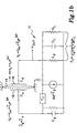
- Source 36 of FET 26 is connected to a reference terminal or ground 31.
- a feedback impedance 38 has one end connected to drain 24 and the other end connected to gate 28 of FET 26.
- Feedback impedance 38 provides a certain amount of negative feedback resulting in a stabilization of a gate bias to FET 26 so that FET 26 functions in a desired region of its performance characteristics.
- Feedback resistor 38 may be a resistor having a value on the order of about 10 8 ohms.
- the output of circuit 10 may be monitored at output 35.
- the description of the present invention is in the context of a field effect transistor or transistors; however, the invention also may be implemented with a bipolar transistor or transistors, or a combination of field effect and bipolar transistors.
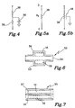
- Figures 5a-c show alternative equivalent circuits for feedback resistor 38.
- Feedback resistor 38 of figure 5a, which is approximately 10 8 ohms and can be implemented using undoped polysilicon, preferably has the polysilicon isolated by nitride to avoid high impedance DC paths to ground, especially at high temperatures. In order to prevent drain-to-gate feedback, low AC impedance paths to ground should be provided.
- the capacitance of nitride provides such a distributed capacitance 48 as indicated in figure 5b, but it may be necessary to provide additional capacitance 50 as indicated in figure 4.
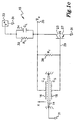
- Configuration 52 uses a twisting or bending mode of beam 54 which has oppositely-located side plates 56 and 53 attached like the wings of an airplane.
- Drive electrode 16 and sense electrode 18 are both located facing the same side (i.e., both above or both below wings 56 and 53, respectively, so that one capacitor is decreasing while the capacitor on the opposite side is increasing.
- the phase relationship is the same when electrodes 16 and 18 are located above and below the beam as in figure 2.
- Beam 54 and localized regions of the shell above beam 54 are grounded, so that there is good electrical isolation between the drive electrode 16 and sense electrode 18 or between gate 28 and drain 24, as desired.
- the above-provided analysis applies in the case of configuration 52.
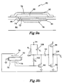
- Figure 9a is a side cross-section view of a double beam resonant integrated microbeam sensor 80.
- Device 80 may be micromachined using polysilicon films. Situated in substrate 82 is drive electrode 76. Proximate to substrate 82 is lower cavity 84, and adjacent to cavity 84 is a first microbeam 72 that is secured at both ends as it is an integral part of silicon 82. Parallel to first microbeam 72 is a second microbeam 74 which is a beam piggy-backed to beam 72. Microbeam 74 is secured at both ends as it is micromachined from the same piece of silicon as microbeam 72.
- Figure 9b shows an electronic circuit for double beam RIMS 80.
- Drive electrode 76 has a drive voltage signal causing microbeam 72 to vibrate in a mode at the resonant frequency of the beam.
- Beam 74 vibrates at the same frequency through mechanical coupling from beam 72.
- Beams 72 and 74 are connected to ground.
- the values of the resonant frequencies indicate an amount of longitudinal tension placed on beams 72 and 74 which may indicate a measurement of pressure, acceleration or other physical quantity.
- Sense electrode 78 is proximate to microbeam 74 and electrically detects the vibration of microbeam 74 and passes a vibration indicating signal on to a n-channel transistor 92.
- Transistor 92 amplifies the vibration indicating signal which is coupled with coupling capacitor 94 to a push-pull amplifier having a p-channel transistor 96 and a n-channel transistor 98.
- the gate of transistor 92 is connected to high impedance feedback resistor 102.
- Resistor 102 is connected to the gate of transistor 92.
- the value of resistor 102 is such that biasing of transistor 92 in the linear region is maintained.
- Load resistor 104 and load capacitor 106 are connected in parallel, and connect the drain of transistor 92 to a positive (5 to 12 volt) supply V+.
- the values of resistor 104 and capacitor 106 are dependent on the resonant frequency of microbeams 72 and 74.
- Adjacent to drive and sense lines 114, 116 and 118 is a lower cavity 126.
- microbeam segments 120, 122 and 124 which are in a same silicon layer or plane 132.
- Beam 120 is shown in figure 10a.
- Figures 10b and 10c illustrate the physical relationship of beams 120, 122 and 124.
- Adjacent to beams 120, 122 and 124 is upper cavity 128.
- Over and scaling the volume, that is, lower cavity 126 and upper cavity 128, enclosing beams 120, 122 and 124 is shell 130. Cavities 126 and 128 are maintained in a vacuum.
- Beams 120, 122 and 124 are each secured at both ends of the respective triple microbeam.
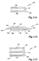
- FIGS 11a and 11b show a microbeam 144 that is connected to substrate 152 at only one end.
- Such microbeam structure 150 has application as a temperature sensor as the resonance frequency of structure 150 would change with respect to the temperature of structure 150.
- Microbeam structure 150 may also be used as an electromechanical filter described above.
- Drive electrode 146 is situated in substrate 152 for driving cantilever beam 144.
- Cantilever beam 144 is connected to pound and forms an electrode having capacitance relative to drive electrode 146, that varies according to distance between beam 144 and electrode 146. This distance varies as beam 144 moves or vibrates.
- Beam 144 is fabricated from a layer 154 with a gap 156. Between beam 144 and drive electrode 146 is a lower cavity 158.
- FIG. 12c A schematic of the dual cantilever beams and associated electronics is revealed by figure 12c.
- the output of the electronics drives beam 166 at a resonant frequency which varies according to the temperature of the beam 166 apparatus.
- the vibration of beam 166 through mechanical coupling, drives beam 168 into a resonant vibration at a frequency which is the same as that of beam 166.
- the vibration of beam 168 is sensed by sense electrode 178 which inputs a signal to the electronics.
- the output of the electronics goes to driver 176 to sustain the vibration of beam 166 and in turn beam 168.
- Electrodes 176 and 178 are on the same side of beams 166 and 168. Beams 166 and 168 vibrate 180 degrees out of phase relative to each other, and the sensed signals are not only amplified but inverted for sending to drive electrode 176.
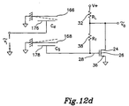
- a dual microbeam filter sensor is shown in figure 12d.
- the beam configuration is the same as that of figure 12c, except the electronics connections to electrodes 176 and 178 are different in that drive electrode 176 receives the signal that is to be filtered.
- This device is a filter at the resonant frequency of beam 166.
- the signal to be filtered goes to drive electrode 176 to drive beam 166.
- Signals having frequencies other than the resonant frequency of beam 166 do not vibrate beam 166 with any significance, and thus the vibration of beam 168 through mechanical coupling is insignificant, or nonexistent and an insignificant or no signal is detected by sense electrode 178.
Landscapes
- Physics & Mathematics (AREA)
- General Physics & Mathematics (AREA)
- Micromachines (AREA)
- Measuring Fluid Pressure (AREA)
- Piezo-Electric Or Mechanical Vibrators, Or Delay Or Filter Circuits (AREA)
Abstract
Description
The present structure makes it possible to take advantage of the greater-than-unity gain to realize a resonant strain transducer which can be augmented by an appropriate microstructure to measure pressure, acceleration, force and other applied stimuli.
then

Claims (52)
- A transistor resonant integrated microbeam structure comprising:a beam having a first end attached to a substrate;a first electrode proximate to said beam to form a first capacitance between said first electrode and said beam, such that when said beam vibrates the first capacitance varies; anda second electrode proximate to said beam to form a capacitance between said second electrode and said beam, such that when said beam vibrates the second capacitance varies 180 degrees out of phase from said first capacitance.
- The microbeam structure of Claim 1 further comprising an inverter having an input connected to said second electrode and having an output connected to said first electrode.
- The microbeam structure of Claim 2 wherein said inverter comprises:a transistor having a first terminal connected to said first electrode, a second terminal connected to said second electrode, and a third terminal connected to said beam; anda load impedance having a first terminal connected to the first terminal of said transistor and having a second terminal connected to a voltage terminal.
- The microbeam structure of Claim 3 further comprising a feedback impedance having a first terminal connected to the first terminal of said transistor and having a second terminal connected to the second terminal of said transistor.
- The microbeam structure of Claim 4 wherein:said first electrode is an electrostatic driver; andsaid second electrode is a capacitive sensor.
- A transistor resonant integrated microbeam structure comprising:a beam situated on a substrate and connected to a reference terminal, said beam having a first end and a second end fastened to the substrate, said beam having tension or compression between the first and second ends, caused by a bending of the substrate due to a magnitude of a physical parameter being measured, and said beam capable of vibrating at a resonant frequency dependent on the tension or compression of said beam, the resonant frequency indicating the magnitude of the physical parameter being measured;a first electrode situated near a first side of said beam, such that when said beam vibrates, a distance between said beam and said first electrode varies, and a first capacitance between said first electrode and said beam varies with vibration of said beam;a second electrode situated on a second side of said beam, the second side being the opposite side of the first side of said beam, such that when said beam vibrates, a distance between said beam and said second electrode varies oppositely to the distance between said beam and said first electrode, and a second capacitance between said second electrode and said beam varies inversely to the first capacitance between said first electrode and said beam; andan inverter having an input connected to said first electrode and an output connected to said second electrode.
- The microbeam structure of claim 6 wherein said inverter comprises:a transistor having a first terminal connected to said first electrode, a second terminal connected to said second electrode, and a third terminal connected to the reference terminal; anda load impedance having a first terminal connected to the second terminal of said transistor and having a second terminal connected to a voltage terminal.
- The microbeam structure of claim 7 further comprising a feedback impedance having a first terminal connected to the first terminal of said transistor and having a second terminal connected to the second terminal of said transistor.
- The microbeam structure of claim 8 wherein:said first electrode is a capacitive sensor; andsaid second electrode is an electrostatic driver.
- The microbeam structure of claim 9 wherein:said transistor is an N-channel field effect transistor; andthe first, second and third terminals of said transistor are a gate, a drain and a source, respectively.
- The microbeam structure of claim 9 wherein:said transistor is a bipolar transistor; andthe first, second and third terminals of said transistor are a base, a collector and a emitter, respectively.
- The microbeam structure of claim 10 wherein said load impedance comprises a resistor and a capacitor connected in parallel with each other.
- An integrated microbeam structure comprising:a beam structure situated in a substrate;a driving means, proximate to said beam structure, for driving said beam structure into vibration, according to a driving signal;a sensing means, proximate to said beam structure, for sensing vibration of said beam structure and providing a sensing signal; anda circuit means, connected to said driving means and said sensing means, for converting the sensing signal from said sensing means into a driving signal for said driving means.
- The microbeam structure of claim 13, wherein:said beam structure has a resonant frequency; andthe resonant frequency indicates a magnitude of a parameter which affects said beam structure which in turn affects the resonant frequency.
- A transistor resonant integrated microbeam structure comprising:a beam situated in a substrate and connected to a reference terminal, said beam having a first end and a second end fastened to the substrate, said beam having a tension or compression between the first and second ends and caused by bending of the substrate due to a magnitude of a physical parameter being measured, and said beam having a resonant frequency affected according to an amount of tension or compression of said beam, the resonant frequency indicating the magnitude of the physical parameter;a first electrode situated on a first side of said beam, such that when said beam vibrates, a distance between said beam and said first electrode varies in synchronism with the resonant frequency, resulting in a first capacitance between said first electrode and said beam that varies inversely with the distance between said first electrode and said beam;a second electrode situated on the first side of said beam, a distance between said beam and said second electrode varies proportionally to the distance between said beam and said first electrode, and a second capacitance between said second electrode and said beam varies in phase with the first capacitance; anda non-inverter having an input connected to said first electrode and an output connected to said second electrode.
- The microbeam structure of claim 15 wherein said non-inverter comprises:a first transistor having a first terminal connected to said first electrode, a second terminal connected to the reference terminal, and a third terminal; andan inverter having an input terminal connected to the third terminal of said transistor and having an output terminal connected to said second electrode.
- The microbeam structure of claim 16 further comprising a feedback impedance having a first terminal connected to the first terminal of said first transistor and having a second terminal connected to said third electrode.
- The microbeam structure of claim 17 wherein:said first electrode is a sense electrode; andsaid second electrode is a driver electrode.
- The microbeam structure of claim 18 wherein said inverter comprises:a second transistor having a first terminal connected to the third terminal of said first transistor, having a second terminal connected to the first terminal of said second transistor, and having a third terminal connected to a voltage terminal;a third transistor having a first terminal connected to said second electrode, having a second terminal connected to the second terminal of said second transistor, and having a third terminal connected to the voltage terminal; andan impedance having a first terminal connected to the first terminal of said third transistor and having a second terminal connected to the reference terminal.
- The microbeam structure of claim 15 wherein said non-inverter comprises:a transistor having a first terminal connected to said first electrode, a second terminal connected to a voltage terminal, and a third terminal connected to said second electrode; anda load impedance having a first terminal connected to the third terminal of said transistor and a second terminal connected to the reference terminal.
- The microbeam structure of claim 20 wherein said non-inverter further comprises a feedback impedance having a first terminal connected to the first terminal of said transistor and having a second terminal connected to the second terminal of said transistor.
- The microbeam structure of claim 21 wherein:said transistor is an N-channel field effect transistor; andthe first, second and third terminals of said transistor are a gate, a drain and a source, respectively.
- The microbeam structure of claim 21 wherein:said transistor is a bipolar transistor; andthe first, the second, and third terminals of said transistor are a base, a collector and an emitter, respectively.
- A transistor resonant integrated microbeam structure comprising:a first beam situated in a substrate and connected to a reference terminal, said first beam having a first end and a second end fastened to the substrate, said first beam having a tension or compression between the first and second ends which is caused by a bending of the substrate due to a magnitude of a physical parameter being measured, and said first beam having a resonant frequency dependent upon an amount of tension or compression of said first beam, the resonant frequency indicating the magnitude of the physical parameter;a second beam situated proximate to said first beam and connected to the reference terminal, said second beam having a first end and a second end fastened at the first and second ends of said first beam, said second beam being parallel to and at a distance from said first beam, said second beam having a tension or compression like that of said first beam, said second beam being mechanically coupled to said first beam so when said first beam vibrates, said second beam vibrates at a resonant frequency that is the same as the resonant frequency of said first beam, and vibrates 180 degrees out of phase relative to said first beam;a first electrode situated proximate to a first side of said first beam which is opposite to a second side of said first beam that is proximate to said second beam, said first electrode at a first distance that varies with respect to said first beam when said first beam vibrates, and said first electrode having a first capacitance relative to said first beam, that varies inversely to the first distance, at the resonant frequency of said first beam;a second electrode situated proximate to a first side of said second beam opposite to a second side of said second beam that is proximate to said first beam, said second electrode at a second distance that varies with respect to said second beam when said second beam vibrates, and said second electrode having a second capacitance relative to said second beam, that varies inversely to the second distance, at the resonant frequency of said second beam; anda noninverter having an input connected to said second electrode and an output connected to said first electrode.
- The microbeams structure of claim 24 wherein said noninverter comprises:a first transistor having a first terminal connected to said second electrode, a second terminal connected to the reference terminal and having a third terminal;a load impedance having a first terminal connected to the third terminal of said first transistor and having a second terminal connected to a first voltage terminal; andan inverter having an input terminal connected to the third terminal of said first transistor and having an output terminal connected to said first electrode.
- The microbeam structure of claim 25 further comprising a feedback impedance having a first terminal connected to the third terminal of said first transistor and having a second terminal connected to first terminal of said first transistor.
- The microbeam structure of claim 25 wherein:said first electrode is a driver electrode; andsaid second electrode is a sensor electrode.
- The microbeam structure of claim 27 wherein said inverter comprises:a second transistor having a first terminal, having a second terminal connected to the output terminal of said inverter and having a third terminal connected to a second voltage terminal;a third transistor having a first terminal connected to the first terminal of a said second transistor, having a second terminal connected to the reference terminal, and having a third terminal connected to the second terminal of said second transistor; andan input impedance having a first terminal connected to the input terminal of said inverter and having a second terminal connected to the first terminal of said second and third transistors.
- The microbeam structure of claim 24 wherein said noninverter comprises:a transistor having a first terminal connected to the input terminal of said noninverter, a second terminal connected to a voltage terminal, and a third terminal connected to the output terminal of said noninverter; anda load impedance having a first terminal connected to the third terminal of said transistor and a second terminal connected to the reference terminal.
- The microbeam structure of claim 29 wherein said non-inverter further comprises a feedback impedance having a first terminal connected to the first terminal of said transistor and having a second terminal connected to the second terminal of said transistor.
- The microbeam structure of claim 30 wherein:said transistor is an N-channel field effect transistor; andthe first, second and third terminals of said transistor are a gate, a drain and a source, respectively.
- The microbeam structure of claim 30 wherein:said transistor is a bipolar transistor; andthe first, the second, and third terminals of said transistor are a base, a collector and an emitter, respectively.
- A transistor resonant integrated microbeam structure comprising:a first beam, capable of vibrating, situated in a substrate;a second beam, capable of vibrating, situated in the substrate, adjacent to said first beam;a third beam, capable of vibrating, situated in the substrate, adjacent to said second beam;a first electrode, proximate to said first beam, having a capacitance relative to said first beam, the capacitance having a value that varies with vibrating movement of said first beam;a second electrode, proximate to said second beam, having a capacitance relative to said second beam, the capacitance having a value that varies with vibrating movement of said second beam;a third electrode, proximate to said third beam, having a capacitance relative to said third beam, the capacitance having a value that varies with vibrating movement of said third beam; andan inverter having an input connected to said first and third electrodes and an output connected to said second electrode; and
wherein:said first, second and third beams have ends fastened to the substrate and connected to a reference terminal, have a resonant frequency that varies relative to a tension or compression applied at the ends to said first, second and third beams, the tension or compression caused by a physical phenomenon having a magnitude, and the resonant frequency being an indication of the magnitude of the physical phenomenon. - The microbeam structure of claim 33 wherein said inverter comprises:a transistor having a first terminal connected to the input of said inverter, a second terminal connected to a reference terminal and a third terminal connected to the output of said inverter; anda load impedance having a first terminal connected to the third terminal of said transistor and having a second terminal connected to a voltage terminal.
- The microbeam structure of claim 34 wherein:said first and third electrodes are capacitive sensing electrodes that sense vibrating movement of said first and third beams, respectively;said second electrode is an electrostatic driving electrode that drives said second beam to vibrating movement at the resonant frequency; andsaid first and third beams are driven to vibrating movement at the resonant frequency through a mechanical coupling because of proximity to said second beam when vibrating.
- The microbeam structure of claim 35 further comprising a feedback resistor having first and second terminals connected to first and third terminals, respectively, of said transistor.
- The microbeam structure of claim 36 wherein:said transistor is an N-channel field effect transistor; andthe first, second and third terminals of said transistor are a gate, a source and a drain, respectively.
- The microbeam structure of claim 36 wherein:said transistor is a bipolar transistor; andthe first, the second, and third terminals of said transistor are a base, an emitter and a collector, respectively.
- A transistor resonant integrated microbeam structure comprising:a beam having first end attached to a substrate and having a second end that is free to vibrate;a first electrode proximate to said beam to form a first capacitance between said first electrode and said beam, such that when said beam vibrates the first capacitance varies; anda second electrode proximate to said beam to form a capacitance between said second electrode and said beam, such that when said beam vibrates the second capacitance varies 180 degrees out of phase from said first capacitance.
- The microbeam structure of claim 31 further comprising an inverter having an input connected to said second electrode and having an output connected to said first electrode.
- The microbeam structure of claim 40 wherein said inverter comprises:a transistor having a first terminal connected to said first electrode, a second terminal connected to said second electrode, and a third terminal connected to said beam; anda load impedance having a first terminal connected to the first terminal of said transistor and having a second terminal connected to a voltage terminal.
- The microbeam structure of claim 41 further comprising a feedback impedance having a first terminal connected to the first terminal of said transistor and having a second terminal connected to the second terminal of said transistor.
- The microbeam structure of claim 42 wherein:said first electrode is an electrostatic driver; andsaid second electrode is a capacitive sensor.
- A transistor resonant integrated microbeam structure comprising:at least one beam attached to a substrate with at least one end of said at least one beam;an electrostatic drive electrode proximate to said at least one beam, for driving said at least one beam into vibration;a capacitive sense electrode proximate to said at least one beam, for sensing vibration of said at least one beam; andan buffer/amplifier circuit having an input connected to said capacitive sense electrode.
- The microbeam structure of claim 44 wherein said buffer/amplifier circuit has an output connected to said electrostatic drive electrode.
- A transistor resonant integrated microbeam structure comprising:a plurality of beams, wherein each beam of said plurality of beams is attached to a substrate with at least one end of each beam, and each beam is proximate to at least one other beam of said plurality of beams such that vibration of each beam can be mechanically coupled to the at least one other beam;at least one capacitive sense electrode proximate to at least one of said plurality of beams;at least one electrostatic drive electrode proximate to at least one of said plurality of beams; anda circuit having an input connected to said at least one capacitive sense electrode.
- The microbeam structure of claim 46 wherein said circuit has an output connected to said least one electrostatic drive electrode.
- The microbeam structure of claim 47 wherein said circuit is an inverter.
- The microbeam structure of claim 48 wherein said inverter comprises:a transistor having a first terminal connected to the input of said circuit, a second terminal connected to the output of said circuit, and a third terminal electrically connected to said plurality of beams;a load impedance having a first terminal connected to the second terminal of said transistor and having a second terminal connected to a voltage terminal; anda feedback impedance having a first terminal connected to the first terminal of said transistor and having a second terminal connected to the second terminal of said transistor.
- The microbeam structure of claim 49 wherein:said transistor is an N-channel field effect transistor; andthe first, second and third terminals of said transistor are a gate, a drain and a source, respectively.
- The microbeam structure of claim 49 wherein:said transistor is a bipolar transistor; andthe first, second and third terminals are a base, a collector and an emitter, respectively.
- The microbeam structure of claim 47 wherein said circuit provides a drive voltage to at least one electrostatic drive electrode proximate to at least one of said plurality of beams, the drive voltage having a component in phase with a velocity of the at least one of said plurality of beams.
Applications Claiming Priority (3)
| Application Number | Priority Date | Filing Date | Title |
|---|---|---|---|
| US357943 | 1994-12-16 | ||
| US08/357,943 US5550516A (en) | 1994-12-16 | 1994-12-16 | Integrated resonant microbeam sensor and transistor oscillator |
| EP95943138A EP0797758B1 (en) | 1994-12-16 | 1995-12-15 | Integrated resonant microbeam sensor and transistor oscillator |
Related Parent Applications (1)
| Application Number | Title | Priority Date | Filing Date |
|---|---|---|---|
| EP95943138A Division EP0797758B1 (en) | 1994-12-16 | 1995-12-15 | Integrated resonant microbeam sensor and transistor oscillator |
Publications (2)
| Publication Number | Publication Date |
|---|---|
| EP1026491A2 true EP1026491A2 (en) | 2000-08-09 |
| EP1026491A3 EP1026491A3 (en) | 2001-01-31 |
Family
ID=23407670
Family Applications (3)
| Application Number | Title | Priority Date | Filing Date |
|---|---|---|---|
| EP00201303A Withdrawn EP1026491A3 (en) | 1994-12-16 | 1995-12-15 | Integrated resonant microbeam sensor and transistor oscillator |
| EP01201984A Withdrawn EP1132728A3 (en) | 1994-12-16 | 1995-12-15 | Integrated resonant microbeam sensor and transistor oscillator |
| EP95943138A Expired - Lifetime EP0797758B1 (en) | 1994-12-16 | 1995-12-15 | Integrated resonant microbeam sensor and transistor oscillator |
Family Applications After (2)
| Application Number | Title | Priority Date | Filing Date |
|---|---|---|---|
| EP01201984A Withdrawn EP1132728A3 (en) | 1994-12-16 | 1995-12-15 | Integrated resonant microbeam sensor and transistor oscillator |
| EP95943138A Expired - Lifetime EP0797758B1 (en) | 1994-12-16 | 1995-12-15 | Integrated resonant microbeam sensor and transistor oscillator |
Country Status (6)
| Country | Link |
|---|---|
| US (1) | US5550516A (en) |
| EP (3) | EP1026491A3 (en) |
| JP (1) | JP3694028B2 (en) |
| CA (1) | CA2205904C (en) |
| DE (1) | DE69528284T2 (en) |
| WO (1) | WO1996018873A1 (en) |
Cited By (3)
| Publication number | Priority date | Publication date | Assignee | Title |
|---|---|---|---|---|
| EP1202046A1 (en) * | 2000-10-25 | 2002-05-02 | Abb Research Ltd. | Method and apparatus for determining biological species |
| EP1530036A1 (en) * | 2003-11-07 | 2005-05-11 | VARIAN S.p.A. | Pressure sensor |
| EP1722210A2 (en) | 2005-05-10 | 2006-11-15 | VARIAN S.p.A. | Pressure sensor with a vibrating member |
Families Citing this family (49)
| Publication number | Priority date | Publication date | Assignee | Title |
|---|---|---|---|---|
| US5491604A (en) * | 1992-12-11 | 1996-02-13 | The Regents Of The University Of California | Q-controlled microresonators and tunable electronic filters using such resonators |
| US6118124A (en) * | 1996-01-18 | 2000-09-12 | Lockheed Martin Energy Research Corporation | Electromagnetic and nuclear radiation detector using micromechanical sensors |
| US5844238A (en) * | 1996-03-27 | 1998-12-01 | David Sarnoff Research Center, Inc. | Infrared imager using room temperature capacitance sensor |
| US5811807A (en) * | 1996-07-19 | 1998-09-22 | Ail Systems, Inc. | Uncooled background limited detector and method |
| US5808210A (en) * | 1996-12-31 | 1998-09-15 | Honeywell Inc. | Thin film resonant microbeam absolute pressure sensor |
| US5747705A (en) * | 1996-12-31 | 1998-05-05 | Honeywell Inc. | Method for making a thin film resonant microbeam absolute |
| US6630852B2 (en) * | 1997-06-17 | 2003-10-07 | Seiko Epson Corporation | Power-generation detection circuit for use in an electronic device and power-generation detection method and power consumption control method for use in connection therewith |
| US6031944A (en) * | 1997-12-30 | 2000-02-29 | Honeywell Inc. | High temperature resonant integrated microstructure sensor |
| US5955659A (en) * | 1998-01-13 | 1999-09-21 | Massachusetts Institute Of Technology | Electrostatically-actuated structures for fluid property measurements and related methods |
| US6050722A (en) * | 1998-03-25 | 2000-04-18 | Thundat; Thomas G. | Non-contact passive temperature measuring system and method of operation using micro-mechanical sensors |
| US6140646A (en) * | 1998-12-17 | 2000-10-31 | Sarnoff Corporation | Direct view infrared MEMS structure |
| WO2000040938A1 (en) | 1999-01-08 | 2000-07-13 | Sarnoff Corporation | Optical detectors using nulling for high linearity and large dynamic range |
| US6713938B2 (en) | 1999-01-14 | 2004-03-30 | The Regents Of The University Of Michigan | Method and apparatus for filtering signals utilizing a vibrating micromechanical resonator |
| US6424074B2 (en) | 1999-01-14 | 2002-07-23 | The Regents Of The University Of Michigan | Method and apparatus for upconverting and filtering an information signal utilizing a vibrating micromechanical device |
| US6593831B2 (en) | 1999-01-14 | 2003-07-15 | The Regents Of The University Of Michigan | Method and apparatus for filtering signals in a subsystem including a power amplifier utilizing a bank of vibrating micromechanical apparatus |
| US6600252B2 (en) * | 1999-01-14 | 2003-07-29 | The Regents Of The University Of Michigan | Method and subsystem for processing signals utilizing a plurality of vibrating micromechanical devices |
| US6249073B1 (en) | 1999-01-14 | 2001-06-19 | The Regents Of The University Of Michigan | Device including a micromechanical resonator having an operating frequency and method of extending same |
| US6577040B2 (en) | 1999-01-14 | 2003-06-10 | The Regents Of The University Of Michigan | Method and apparatus for generating a signal having at least one desired output frequency utilizing a bank of vibrating micromechanical devices |
| US6566786B2 (en) | 1999-01-14 | 2003-05-20 | The Regents Of The University Of Michigan | Method and apparatus for selecting at least one desired channel utilizing a bank of vibrating micromechanical apparatus |
| SE9902114D0 (en) * | 1999-06-07 | 1999-06-07 | Astra Ab | Electrical device |
| US6446012B1 (en) * | 1999-06-23 | 2002-09-03 | Bfcs Technology, Inc. | Proximity detector for hard-to-detect materials |
| IT1318295B1 (en) * | 2000-07-31 | 2003-07-28 | Abb Ricerca Spa | DEVICE FOR MEASURING THE PRESSURE OF A FLUID |
| US6584857B1 (en) | 2000-11-20 | 2003-07-01 | Eastman Kodak Company | Optical strain gauge |
| US6487913B2 (en) | 2000-12-18 | 2002-12-03 | Eastman Kodak Company | Strain gauge with resonant light modulator |
| WO2004032320A1 (en) * | 2002-10-03 | 2004-04-15 | Sharp Kabushiki Kaisha | Microresonator, microfilter, micro-oscillator, and wireless communication device |
| JP4058529B2 (en) | 2003-09-08 | 2008-03-12 | 株式会社デンソーウェーブ | Optical information reader |
| CN100547921C (en) * | 2004-04-28 | 2009-10-07 | 松下电器产业株式会社 | Electromechanical filter |
| JP4602130B2 (en) * | 2004-04-28 | 2010-12-22 | パナソニック株式会社 | Electromechanical filter |
| US7176048B1 (en) * | 2004-12-12 | 2007-02-13 | Burns David W | Optically coupled sealed-cavity resonator and process |
| US7443509B1 (en) | 2004-12-12 | 2008-10-28 | Burns David W | Optical and electronic interface for optically coupled resonators |
| US7605391B2 (en) * | 2004-12-12 | 2009-10-20 | Burns David W | Optically coupled resonator |
| US7499604B1 (en) | 2004-12-12 | 2009-03-03 | Burns David W | Optically coupled resonant pressure sensor and process |
| US7379629B1 (en) | 2004-12-12 | 2008-05-27 | Burns David W | Optically coupled resonant pressure sensor |
| CN100568720C (en) * | 2005-01-13 | 2009-12-09 | 松下电器产业株式会社 | Torsional resonators and filters using them |
| GB0517340D0 (en) * | 2005-08-25 | 2005-10-05 | Avery Berkel Ltd | Improvements in or relating to vibrating beam sensors |
| EP1840527A1 (en) * | 2006-03-27 | 2007-10-03 | Infineon Technologies SensoNor AS | Displacement sensor with frequency output |
| US8026779B2 (en) * | 2006-06-14 | 2011-09-27 | Panasonic Corporation | Vibrator, resonator using the same and electromechanical filter using the same |
| FR2916533B1 (en) | 2007-05-25 | 2012-12-28 | Thales Sa | SYSTEM FOR FREQUENCY ANALYSIS OF RESONANT DEVICES. |
| JP5135628B2 (en) * | 2007-08-31 | 2013-02-06 | セイコーインスツル株式会社 | Oscillator and oscillator using the same |
| US20100327993A1 (en) * | 2008-02-21 | 2010-12-30 | Sanyo Electric Co., Ltd. | Micro mechanical resonator |
| JP5101410B2 (en) * | 2008-06-27 | 2012-12-19 | セイコーインスツル株式会社 | Resonant frequency variable MEMS vibrator |
| FR2939581B1 (en) * | 2008-12-09 | 2010-11-26 | Commissariat Energie Atomique | NETWORK OF COUPLED RESONATORS, PASS-BAND FILTER AND OSCILLATOR. |
| FR2942681B1 (en) * | 2009-02-27 | 2011-05-13 | Commissariat Energie Atomique | MICROMETRIC OR NANOMETRIC RESONANT DEVICE WITH TRANSISTORS |
| FR2942682A1 (en) * | 2009-02-27 | 2010-09-03 | Commissariat Energie Atomique | DEVICE RESULTING IN IMPROVED CHARACTERISTICS |
| US8115573B2 (en) * | 2009-05-29 | 2012-02-14 | Infineon Technologies Ag | Resonance frequency tunable MEMS device |
| JP2014170998A (en) * | 2013-03-01 | 2014-09-18 | Seiko Epson Corp | Mems element, electronic device, electronic apparatus, and mobile |
| US9285207B2 (en) * | 2013-03-13 | 2016-03-15 | Invensense, Inc. | Linear capacitive displacement sensor |
| WO2015195024A1 (en) * | 2014-06-18 | 2015-12-23 | Sondero Technologies Ab | Device for measuring vibration frequency |
| RU2693928C1 (en) * | 2018-08-21 | 2019-07-05 | Общество с ограниченной ответственностью "Научно-Технический Центр "Завод Балансировочных Машин" | Device for transmitting analogue signals from sensors along a two-wire line |
Family Cites Families (8)
| Publication number | Priority date | Publication date | Assignee | Title |
|---|---|---|---|---|
| US3585466A (en) * | 1968-12-10 | 1971-06-15 | Westinghouse Electric Corp | Resonant gate transistor with improved gain having a vibratory member disposed in a spaced relationship between a field responsive member and a field plate |
| GB1408619A (en) * | 1971-11-26 | 1975-10-01 | Citizen Watch Co Ltd | Electrostatic oscillating device |
| EP0080022B1 (en) * | 1981-11-20 | 1986-03-12 | Siemens-Albis Aktiengesellschaft | Oscillating device |
| GB2115551B (en) * | 1982-02-09 | 1985-11-13 | Itt Ind Ltd | Load sensor |
| US4901586A (en) * | 1989-02-27 | 1990-02-20 | Sundstrand Data Control, Inc. | Electrostatically driven dual vibrating beam force transducer |
| US5090254A (en) * | 1990-04-11 | 1992-02-25 | Wisconsin Alumni Research Foundation | Polysilicon resonating beam transducers |
| US5275055A (en) * | 1992-08-31 | 1994-01-04 | Honeywell Inc. | Resonant gauge with microbeam driven in constant electric field |
| DE4300893A1 (en) * | 1993-01-15 | 1994-07-21 | Bosch Gmbh Robert | Press. sensor for ultra-high vacuum pressure container |
-
1994
- 1994-12-16 US US08/357,943 patent/US5550516A/en not_active Expired - Lifetime
-
1995
- 1995-12-15 EP EP00201303A patent/EP1026491A3/en not_active Withdrawn
- 1995-12-15 DE DE69528284T patent/DE69528284T2/en not_active Expired - Fee Related
- 1995-12-15 CA CA002205904A patent/CA2205904C/en not_active Expired - Fee Related
- 1995-12-15 EP EP01201984A patent/EP1132728A3/en not_active Withdrawn
- 1995-12-15 EP EP95943138A patent/EP0797758B1/en not_active Expired - Lifetime
- 1995-12-15 JP JP51930196A patent/JP3694028B2/en not_active Expired - Lifetime
- 1995-12-15 WO PCT/US1995/016441 patent/WO1996018873A1/en not_active Ceased
Cited By (5)
| Publication number | Priority date | Publication date | Assignee | Title |
|---|---|---|---|---|
| EP1202046A1 (en) * | 2000-10-25 | 2002-05-02 | Abb Research Ltd. | Method and apparatus for determining biological species |
| EP1530036A1 (en) * | 2003-11-07 | 2005-05-11 | VARIAN S.p.A. | Pressure sensor |
| EP1808685A2 (en) | 2003-11-07 | 2007-07-18 | VARIAN S.p.A. | Pressure sensor with vibrating member |
| EP1808685A3 (en) * | 2003-11-07 | 2008-11-12 | VARIAN S.p.A. | Pressure sensor with vibrating member |
| EP1722210A2 (en) | 2005-05-10 | 2006-11-15 | VARIAN S.p.A. | Pressure sensor with a vibrating member |
Also Published As
| Publication number | Publication date |
|---|---|
| WO1996018873A1 (en) | 1996-06-20 |
| EP1132728A2 (en) | 2001-09-12 |
| EP0797758A1 (en) | 1997-10-01 |
| EP1026491A3 (en) | 2001-01-31 |
| US5550516A (en) | 1996-08-27 |
| DE69528284D1 (en) | 2002-10-24 |
| JPH10512046A (en) | 1998-11-17 |
| EP0797758B1 (en) | 2002-09-18 |
| DE69528284T2 (en) | 2003-05-08 |
| EP1132728A3 (en) | 2001-09-19 |
| CA2205904C (en) | 2009-05-26 |
| JP3694028B2 (en) | 2005-09-14 |
| CA2205904A1 (en) | 1996-06-20 |
Similar Documents
| Publication | Publication Date | Title |
|---|---|---|
| EP0797758B1 (en) | Integrated resonant microbeam sensor and transistor oscillator | |
| US6997054B2 (en) | Capacitance-type inertial detecting device | |
| CA2171188C (en) | Resonant guage with microbeam driven in constant electric field | |
| US6452427B1 (en) | Dual output capacitance interface circuit | |
| US7427819B2 (en) | Film-bulk acoustic wave resonator with motion plate and method | |
| US5377524A (en) | Self-testing capacitive pressure transducer and method | |
| Welham et al. | A laterally driven micromachined resonant pressure sensor | |
| US9300227B2 (en) | Monolithic body MEMS devices | |
| US6874363B1 (en) | Trapped charge field bias vibrating beam accelerometer | |
| US20070089513A1 (en) | Resonator based transmitters for capacitive sensors | |
| US5969257A (en) | Pressure measuring membrane with resonant element vibrating orthogonal to membrane movement | |
| US5339698A (en) | Vibrating beam force transducer with automatic adjustment of its electromagnetic drive | |
| US5417120A (en) | Vibrating beam force transducer with automatic drive control | |
| Qin et al. | A wide temperature range weakly coupled resonant micro-pressure sensor | |
| Bontemps et al. | 56 MHZ piezoresistive micromechanical oscillator | |
| WO2005101029A1 (en) | Mechanical amount sensor | |
| Ghavanini et al. | An easy-to-implement method for evaluation of capacitive resonant sensors | |
| JPH06102123A (en) | Pressure sensor | |
| Huang et al. | An ultrasound source based on a micro-machined electromechanical resonator | |
| JPS6294988A (en) | Field effect pressure sensor | |
| Aslinezhad et al. | A wideband symmetrical piezoelectric vibration sensor based on Gaussian electrode distribution with interface circuit | |
| Do et al. | Low power sub-milligram resonant MEMS load sensor | |
| Erbes et al. | Vacuum Packaged Low-Power Resonant MEMS Strain Sensor | |
| JPH0471447B2 (en) | ||
| Elwenspoek et al. | Force and Pressure sensors |
Legal Events
| Date | Code | Title | Description |
|---|---|---|---|
| PUAI | Public reference made under article 153(3) epc to a published international application that has entered the european phase |
Free format text: ORIGINAL CODE: 0009012 |
|
| 17P | Request for examination filed |
Effective date: 20000427 |
|
| AC | Divisional application: reference to earlier application |
Ref document number: 797758 Country of ref document: EP |
|
| AK | Designated contracting states |
Kind code of ref document: A2 Designated state(s): DE FR GB |
|
| RIN1 | Information on inventor provided before grant (corrected) |
Inventor name: BURNS, DAVID W. |
|
| PUAL | Search report despatched |
Free format text: ORIGINAL CODE: 0009013 |
|
| AK | Designated contracting states |
Kind code of ref document: A3 Designated state(s): DE FR GB |
|
| RIC1 | Information provided on ipc code assigned before grant |
Free format text: 7G 01L 9/00 A, 7H 03B 5/30 B |
|
| AKX | Designation fees paid |
Free format text: DE FR GB |
|
| GRAP | Despatch of communication of intention to grant a patent |
Free format text: ORIGINAL CODE: EPIDOSNIGR1 |
|
| STAA | Information on the status of an ep patent application or granted ep patent |
Free format text: STATUS: THE APPLICATION IS DEEMED TO BE WITHDRAWN |
|
| 18D | Application deemed to be withdrawn |
Effective date: 20100108 |