EP1720381A1 - Organic el panel - Google Patents
Organic el panel Download PDFInfo
- Publication number
- EP1720381A1 EP1720381A1 EP05703691A EP05703691A EP1720381A1 EP 1720381 A1 EP1720381 A1 EP 1720381A1 EP 05703691 A EP05703691 A EP 05703691A EP 05703691 A EP05703691 A EP 05703691A EP 1720381 A1 EP1720381 A1 EP 1720381A1
- Authority
- EP
- European Patent Office
- Prior art keywords
- organic
- panel
- layer
- luminescent layer
- electrode
- Prior art date
- Legal status (The legal status is an assumption and is not a legal conclusion. Google has not performed a legal analysis and makes no representation as to the accuracy of the status listed.)
- Ceased
Links
Images


Classifications
-
- H—ELECTRICITY
- H05—ELECTRIC TECHNIQUES NOT OTHERWISE PROVIDED FOR
- H05B—ELECTRIC HEATING; ELECTRIC LIGHT SOURCES NOT OTHERWISE PROVIDED FOR; CIRCUIT ARRANGEMENTS FOR ELECTRIC LIGHT SOURCES, IN GENERAL
- H05B33/00—Electroluminescent light sources
- H05B33/12—Light sources with substantially two-dimensional radiating surfaces
- H05B33/14—Light sources with substantially two-dimensional radiating surfaces characterised by the chemical or physical composition or the arrangement of the electroluminescent material, or by the simultaneous addition of the electroluminescent material in or onto the light source
-
- A—HUMAN NECESSITIES
- A63—SPORTS; GAMES; AMUSEMENTS
- A63H—TOYS, e.g. TOPS, DOLLS, HOOPS OR BUILDING BLOCKS
- A63H29/00—Drive mechanisms for toys in general
- A63H29/22—Electric drives
-
- A—HUMAN NECESSITIES
- A63—SPORTS; GAMES; AMUSEMENTS
- A63H—TOYS, e.g. TOPS, DOLLS, HOOPS OR BUILDING BLOCKS
- A63H30/00—Remote-control arrangements specially adapted for toys, e.g. for toy vehicles
- A63H30/02—Electrical arrangements
- A63H30/04—Electrical arrangements using wireless transmission
-
- A—HUMAN NECESSITIES
- A63—SPORTS; GAMES; AMUSEMENTS
- A63H—TOYS, e.g. TOPS, DOLLS, HOOPS OR BUILDING BLOCKS
- A63H31/00—Gearing for toys
-
- G—PHYSICS
- G01—MEASURING; TESTING
- G01R—MEASURING ELECTRIC VARIABLES; MEASURING MAGNETIC VARIABLES
- G01R1/00—Details of instruments or arrangements of the types included in groups G01R5/00 - G01R13/00 and G01R31/00
- G01R1/02—General constructional details
- G01R1/06—Measuring leads; Measuring probes
- G01R1/067—Measuring probes
- G01R1/073—Multiple probes
- G01R1/07307—Multiple probes with individual probe elements, e.g. needles, cantilever beams or bump contacts, fixed in relation to each other, e.g. bed of nails fixture or probe card
- G01R1/0735—Multiple probes with individual probe elements, e.g. needles, cantilever beams or bump contacts, fixed in relation to each other, e.g. bed of nails fixture or probe card arranged on a flexible frame or film
-
- H—ELECTRICITY
- H10—SEMICONDUCTOR DEVICES; ELECTRIC SOLID-STATE DEVICES NOT OTHERWISE PROVIDED FOR
- H10K—ORGANIC ELECTRIC SOLID-STATE DEVICES
- H10K50/00—Organic light-emitting devices
- H10K50/10—OLEDs or polymer light-emitting diodes [PLED]
- H10K50/11—OLEDs or polymer light-emitting diodes [PLED] characterised by the electroluminescent [EL] layers
-
- F—MECHANICAL ENGINEERING; LIGHTING; HEATING; WEAPONS; BLASTING
- F16—ENGINEERING ELEMENTS AND UNITS; GENERAL MEASURES FOR PRODUCING AND MAINTAINING EFFECTIVE FUNCTIONING OF MACHINES OR INSTALLATIONS; THERMAL INSULATION IN GENERAL
- F16H—GEARING
- F16H48/00—Differential gearings
- F16H48/06—Differential gearings with gears having orbital motion
- F16H48/08—Differential gearings with gears having orbital motion comprising bevel gears
-
- G—PHYSICS
- G01—MEASURING; TESTING
- G01R—MEASURING ELECTRIC VARIABLES; MEASURING MAGNETIC VARIABLES
- G01R1/00—Details of instruments or arrangements of the types included in groups G01R5/00 - G01R13/00 and G01R31/00
- G01R1/02—General constructional details
- G01R1/06—Measuring leads; Measuring probes
- G01R1/067—Measuring probes
- G01R1/06711—Probe needles; Cantilever beams; "Bump" contacts; Replaceable probe pins
-
- G—PHYSICS
- G01—MEASURING; TESTING
- G01R—MEASURING ELECTRIC VARIABLES; MEASURING MAGNETIC VARIABLES
- G01R3/00—Apparatus or processes specially adapted for the manufacture or maintenance of measuring instruments, e.g. of probe tips
Definitions
- the present invention relates to an organic EL panel comprising a light-transmitting supporting substrate having provided thereon an organic EL (electroluminescence) device comprising an organic layer having at least a luminescent layer, sandwiched with a pair of electrodes.
- organic EL panels using an organic EL device a panel in which the organic EL device is formed by successively laminating a first electrode comprising ITO (Indium Tin Oxide) or the like as an anode, an organic layer having at least a luminescent layer, and a non-light-transmitting second electrode comprising aluminum (Al) or the like as a cathode, on a light-transmitting supporting substrate comprising a glass material is known (see, for example, Patent Document 1).
- ITO Indium Tin Oxide
- Al aluminum
- Such an organic EL panel emits light by injecting holes from the first electrode, injecting electrons from the second electrode, and rebonding the holes and electrons in the luminescent layer, and a long-lived panel that emits light with a given luminance over a long period of time is desired.
- Patent Document 1 JP-A-59-194393
- the invention has an object to provide an organic EL panel that enables the life emitting light with a given luminance for a long period of time to prolong, even in the case of driving in a high current density region.
- the organic EL panel of the invention is an organic EL panel comprising a light-transmitting supporting substrate having formed thereon an organic EL device comprising an organic layer having at least a luminescent layer, sandwiched with a pair of electrodes, characterized in that the luminescent layer has at least a luminescent layer comprising a host material having added thereto a fluorescent material and a transport material as quest materials.
- the transport material has mobility of the holes or electrons of 10 -4 cm 2 /V ⁇ s or more.
- ionization potential of the fluorescent material is a value lower by 0.1 eV or more than ionization potential of the host material.
- the luminescent layer comprises the host material having hole transport property having added thereto the fluorescent material and the transport material having hole transport property as the guest materials.
- the luminescent layer comprises the host material having electron transport property having added thereto the fluorescent material and the transport material having electron transport property as the guest materials.
- the invention relates to an organic EL panel comprising a light-transmitting supporting substrate having provided thereon an organic EL device comprising an organic layer having at least a luminescent layer, sandwiched with a pair of electrodes, and enables the life that emits light with a given luminance for a long period of time to prolong even in the case of driving in a high density current region.
- an organic EL panel A is mainly constituted of a supporting substrate 1, a first electrode (anode) 2, an insulating layer 3, a partition wall part 4, an organic layer 5, a second electrode (cathode) 6, and a sealing member 7.
- the supporting substrate 1 is a light-transmitting glass substrate having a rectangular shape.
- the first electrode 2 is one prepared by forming a light-transmitting conductive material such as ITO (Indium Tin Oxide) on the supporting substrate 1 in a laminar form by a method such as sputtering or deposition, and patterning in a stripe form by, for example, photolithography.
- the first electrode 2 has an anode wiring part 2a and an anode part 2b as shown in Fig. 1(a), and the anode wiring part 2a is provided with an anode terminal part 2c for electrically connecting to an external electric source, at an end thereof.
- the insulating layer 3 comprises an insulating material such as a polyimide type or a phenol type, and is formed on a non-luminescent portion on the supporting substrate 1 in a predetermined form by means such as photolithography.
- the insulating layer 3 is formed between the anode parts 2a of the first electrode 2, and is also formed so as to slightly overlap with the first electrode 2, thereby insulating between the first electrode 2 and the second electrode described after.
- the partition wall part 4 comprises an insulating material such as a phenol type, and its cross section is formed in a reverse-tapered form by means such as photolithography.
- the partition wall part 4 is formed so as to cross nearly perpendicular to the anode part 2b on the first electrode 2 and the insulating layer 3, and is formed in an arc form viewing from the organic EL device forming surface side of the supporting substrate 1 as shown in Fig. 1(a) on the portion corresponding to the cathode wiring part described after on the supporting substrate 1.
- the organic layer 5 is formed on the first electrode 2 and the insulating layer 3, and is formed by successively laminating a hole injection layer 5a, a hole transport layer 5b, a luminescent layer 5c, an electron transport layer 5d and an electron injection layer 5e by means such as deposition method as shown in Fig. 2, thus being a layered form having a film thickness of from 80 to 280 nm.
- the hole injection layer 5a has a function to take in holes from the first electrode 2, and comprises, for example, an amine compound formed in a layered form having a film thickness of from 20 to 80 nm by means such as deposition method. Further, the hole injection layer 5a is that a glass transition temperature is 85°C or higher (further preferably 100°C or higher).
- the hole transport layer 5b has a function to convey the holes to the luminescent layer 5c, and comprises, for example, a triphenyl amine tetramer which is an amine compound, formed in a layered form having a film thickness of from 10 to 60 nm by means such as deposition method. Further, the hole transport layer 5b is that a glass transition temperature is 85°C or higher (further preferably 100°C or higher).
- the luminescent layer 5c comprises a fluorescent material 5g and a hole transport material (transport material) 5h as guest materials doped in a host material 5f by means such as co-deposition method, and formed in a layered form having a film thickness of from 20 to 60 nm, as shown in Fig. 2c.
- the host material 5f can transport holes and electrons, has a function to show emission by transporting the holes and electrons and rebonding, has also the characteristics of hole mobility that hole mobility is high and electron mobility is low, and comprises, for example, distyryl arylene derivatives. Further, the host material 5f is that a glass transition temperature is 85°C or higher (further preferably 100°C or higher).
- the fluorescent material 5g has a function to emit light by reacting to the rebonding of electrons and holes, shows emission of an amber color (orange color), and comprises, for example, Model RD001, a product of Idemitsu Kosan Co., Ltd. It is desirable that doping amount of the fluorescent material 5g is constituted to be in an extent such that concentration quenching does not occur, and in the present practical embodiment, the fluorescent material 5g is added such that concentration in the luminescent layer 5c is from 2 to 8%. Further, ionization potential Ipd of the fluorescent material 5g is a value lower by 0.1 eV or more than ionization potential Iph of the host material 5f (Iph-Ipd ⁇ 0.1 eV).
- the hole transport material 5h comprises, for example, TPTE of a triphenylamine tetramer which is an amine compound, and has the characteristics of hole transport property that hole mobility is high and electron mobility is low, and the hole mobility is 10 -4 cm 2 /V ⁇ s or more. Further, the hole transport material 5h is added such that concentration in the luminescent layer 5c is from 5 to 20%. Further, the hole transport material 5h is that a glass transition temperature is 85°C or higher (further preferably 100°C or higher).
- the electron transport layer 5d has a function to convey electrons to the luminescent layer 5c, and comprises, for example, aluminum quinolinol (Alq3) which is a chelate compound, formed in a layered form having a film thickness of from 20 to 60 nm by deposition method or the like.
- Alq3 aluminum quinolinol
- the electron injection layer 5e has a function to inject electrons from the second electrode 6, and comprises, for example, lithium fluoride (LiF) formed in a layered form having a film thickness of about 1 nm by means such as deposition method.
- LiF lithium fluoride
- the second electrode 6 comprises a conductive material such as aluminum (Al) or magnesium silver (Mg:Ag) formed in a layered form having a film thickness of from 50 to 200 nm by means such as deposition method, and is partitioned in a stripe form by the partition wall part 4, and the cathode part 6b that crosses nearly perpendicular to the arc-shaped cathode wiring part 6a and the transparent electrode 2 is formed (see Fig. 1(a)). Further, the cathode wiring part 6a is electrically connected to a connection wiring part 8.
- the connection wiring part 8a is formed together with the first electrode 2, and comprises the same material of ITO. Further, the connection wiring part 8 has a cathode terminal part 8a formed at the end part, for electrically connecting to an external electric source.
- the organic EL device on which pixels comprising the corresponding portions of the anode part 2b and the cathode part 6b are provided in matrix form is obtained by successively laminating the first electrode 2, the insulating layer 3, the partition wall part 4, the organic layer 5 and the second electrode 6 on the supporting substrate 1.
- the sealing member 7 comprises a flat plate member comprising, for example, a glass material, formed in a concave form by an appropriate method such as sandblast, cutting or etching.
- the sealing member 7 seals the organic EL device with the sealing member 7 and the supporting substrate 1 by air-tightly providing on the supporting substrate 1 through an adhesive 7a comprising, for example, an ultraviolet curing epoxy resin.
- the sealing member 7 is constituted to be slightly smaller than the supporting substrate 1 such that the anode terminal part 2c of the first electrode 2 and the cathode terminal part 8a connected to the second electrode 6 are exposed outwardly.
- the sealing member may be a flat plate form, and in this case, the sealing member is provided on the supporting substrate through a spacer.
- a dot matrix type organic EL panel A which has, as a display part, the organic EL device having pixels comprising the corresponding portions of the anode part 2b and the cathode part 6b provided in matrix form.
- This organic EL panel A obtains emission of amber color by rebonding the holes from the first electrode 2 and the electrons from the second electrode 6 in the luminescent layer 5c.
- the organic EL panel drives by a so-called passive drive by selecting each of the plural anode parts 2b and the plural cathode parts 6b, respectively, formed in a stripe form, applying constant electric current, and flashing the pixels comprising the corresponding portions of the selected anode part 2a and the cathode part 6b.
- the efficiency (current efficiency) of the rebonding of holes and electrons decreases, and holes and electrons, not contributing to emission increase, resulting in accelerating deterioration of an organic material of an organic layer.
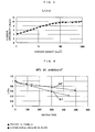
- the hole mobility is higher than the luminescent layer of the conventional organic EL panel, and as shown in Fig. 3, in the case of driving at a high current density region, it is possible to obtain the characteristics that the current efficiency is a value approximating the maximum value or the minimum value.
- the organic EL panel A has high proportion of rebonding between holes and electron in driving in a high current density region. From this, even in the case of driving in a high current density region, holes and electrons, not contributing to emission are smaller than the conventional organic EL panel, and deterioration of an organic material of the organic layer 5 is suppressed. As a result, decrease of emission luminance in the luminescent layer 5c with the passage of time can be suppressed. Fig.
- Characteristic S1 shows characteristics of the conventional organic EL panel
- characteristic S2 shows characteristics of the organic EL panel A of the present practical embodiment. It is apparent from Fig.
- Fig. 5 is the experimental result showing change of emission luminance in the case of applying a predetermined driving voltage to the above-described conventional organic EL panel and organic EL panel A.
- Characteristic S3 shows the characteristics of the conventional organic EL panel
- characteristic S4 shows the characteristics of the organic EL panel A.
- the organic EL panel A is that the organic layer 5 sandwiched with the first electrode 2 and the second electrode 6 has al least the luminescent layer 5c comprising the host material 5f having hole transport property having doped therein, the fluorescent material 5g and the hole transport material 5h. Further, the luminescent layer 5c comprises the host material 5f having doped therein the hole transport material 5h having hole mobility of 10 -4 m 2 /V ⁇ s or more. Further, the luminescent layer 5c is that ionization potential Ipd of the fluorescent material 5g added is a value 0.1 eV lower than ionization potential Iph of the host material 5f.
- the organic EL panel A decreases holes and electrons, not contributing to emission, thereby suppressing deterioration of an organic material of the organic layer 5, and enables the life to prolong so as to emit with a predetermined luminance for a long period of time. Further, the organic EL panel A can obtain a predetermined emission luminance at low voltage as compared with the conventional organic EL panel, and therefore can reduce load to the organic layer 5, making it possible to suppress deterioration of an organic material of the organic layer 5.
- the present practical embodiment is directed to a dot matrix type organic EL panel A, but the invention is applicable to a segment type organic EL panel.
- the organic EL panel A of the present practical embodiment is a constitution having the luminescent layer 5c comprising the host material 5f having hole transport property having doped therein the fluorescent material 5g and the hole transport material 5h, but in the invention, the same effect is obtained in a luminescent layer comprising a host material having electron transport property having doped therein a fluorescent material and a transport material having electron transport property.
- the luminescent layer 5c comprises the host material 5f having doped therein the fluorescent material 5g emitting in amber color, but in the invention, the fluorescent material doped in the host material may be a material emitting in other emitting color.
- the invention is applied to an organic EL panel comprising a light-transmitting supporting substrate having provided thereon an organic EL device comprising an organic layer having at least a luminescent layer, sandwiched with a pair of electrodes.
Abstract
Description
- The present invention relates to an organic EL panel comprising a light-transmitting supporting substrate having provided thereon an organic EL (electroluminescence) device comprising an organic layer having at least a luminescent layer, sandwiched with a pair of electrodes.
- As organic EL panels using an organic EL device, a panel in which the organic EL device is formed by successively laminating a first electrode comprising ITO (Indium Tin Oxide) or the like as an anode, an organic layer having at least a luminescent layer, and a non-light-transmitting second electrode comprising aluminum (Al) or the like as a cathode, on a light-transmitting supporting substrate comprising a glass material is known (see, for example, Patent Document 1).
- Such an organic EL panel emits light by injecting holes from the first electrode, injecting electrons from the second electrode, and rebonding the holes and electrons in the luminescent layer, and a long-lived panel that emits light with a given luminance over a long period of time is desired.
Patent Document 1:JP-A-59-194393 - However, in the case that the organic EL panel is driven in a high current density region of 100 A/m2 or more, there were the problems that time until that emission luminance reduces by half is short, and it is difficult to achieve long-life. As shown in Fig. 6, this is considered due to that by that current efficiency showing the bonding efficiency of the holes injected from the first electrode and the electrons injected from the second electrode in a high current density region, the rebonding proportion of the holes and the electrons in the luminescent layer decreases, thereby electrons and holes that do not contribute to emission increase, and by that the electrons and holes that do not contribute to emission accumulate on the interface of an organic material of the organic layer (for example, the interface between the luminescent layer and a hole transport layer), thereby hastening time that the organic material of the organic layer deteriorates.
- In view of such a problem, the invention has an object to provide an organic EL panel that enables the life emitting light with a given luminance for a long period of time to prolong, even in the case of driving in a high current density region.
- To solve the above-mentioned problems, the organic EL panel of the invention is an organic EL panel comprising a light-transmitting supporting substrate having formed thereon an organic EL device comprising an organic layer having at least a luminescent layer, sandwiched with a pair of electrodes, characterized in that the luminescent layer has at least a luminescent layer comprising a host material having added thereto a fluorescent material and a transport material as quest materials.
- Further, it is characterized in that the transport material has mobility of the holes or electrons of 10-4 cm2/V·s or more.
- Further, it is characterized in that ionization potential of the fluorescent material is a value lower by 0.1 eV or more than ionization potential of the host material.
- Further, it is characterized in that the luminescent layer comprises the host material having hole transport property having added thereto the fluorescent material and the transport material having hole transport property as the guest materials.
- Further, it is characterized in that the luminescent layer comprises the host material having electron transport property having added thereto the fluorescent material and the transport material having electron transport property as the guest materials.
- The invention relates to an organic EL panel comprising a light-transmitting supporting substrate having provided thereon an organic EL device comprising an organic layer having at least a luminescent layer, sandwiched with a pair of electrodes, and enables the life that emits light with a given luminance for a long period of time to prolong even in the case of driving in a high density current region.
-
- [Fig. 1] A view showing an organic EL panel to which the invention was applied.
- [Fig. 2] An enlarged sectional view showing an organic layer of the same as above.
- [Fig. 3] A view showing current efficiency of the organic EL panel of the same as above.
- [Fig. 4] A view showing the relationship between emission time and emission luminance in the organic EL panel of the same as above and the conventional organic EL panel.
- [Fig. 5] A view showing the relationship between driving voltage and emission luminance in the organic EL panel of the same as above and the conventional organic EL panel.
- [Fig. 6] A view showing current efficiency of the conventional organic EL panel.
-
- A
- Organic EL panel
- 1
- Supporting substrate
- 2
- First electrode
- 2a
- Anode wiring part
- 2b
- Anode part
- 2c
- Anode terminal part
- 3
- Insulating layer
- 4
- Partition wall part
- 5
- Organic layer
- 5a
- Hole injection layer
- 5b
- Hole transport layer
- 5c
- Luminescent layer
- 5d
- Electron transport layer
- 5e
- Electron injection layer
- 5f
- Host material
- 5g
- Fluorescent material
- 5h
- Hole transport material (transport material)
- 6
- Second electrode
- 6a
- Cathode wiring part
- 6b
- Cathode part
- 7
- Sealing member
- 7a
- Adhesive
- 8
- Connection wiring part
- 8a
- Cathode terminal part
- The practical embodiment in which the invention was applied to a dot matrix type organic EL panel is described below based on the accompanying drawings.
- In Fig. 1, an organic EL panel A is mainly constituted of a supporting
substrate 1, a first electrode (anode) 2, an insulatinglayer 3, apartition wall part 4, anorganic layer 5, a second electrode (cathode) 6, and a sealingmember 7. - The supporting
substrate 1 is a light-transmitting glass substrate having a rectangular shape. - The
first electrode 2 is one prepared by forming a light-transmitting conductive material such as ITO (Indium Tin Oxide) on the supportingsubstrate 1 in a laminar form by a method such as sputtering or deposition, and patterning in a stripe form by, for example, photolithography. Thefirst electrode 2 has ananode wiring part 2a and ananode part 2b as shown in Fig. 1(a), and theanode wiring part 2a is provided with ananode terminal part 2c for electrically connecting to an external electric source, at an end thereof. - The insulating
layer 3 comprises an insulating material such as a polyimide type or a phenol type, and is formed on a non-luminescent portion on the supportingsubstrate 1 in a predetermined form by means such as photolithography. The insulatinglayer 3 is formed between theanode parts 2a of thefirst electrode 2, and is also formed so as to slightly overlap with thefirst electrode 2, thereby insulating between thefirst electrode 2 and the second electrode described after. - The
partition wall part 4 comprises an insulating material such as a phenol type, and its cross section is formed in a reverse-tapered form by means such as photolithography. Thepartition wall part 4 is formed so as to cross nearly perpendicular to theanode part 2b on thefirst electrode 2 and the insulatinglayer 3, and is formed in an arc form viewing from the organic EL device forming surface side of the supportingsubstrate 1 as shown in Fig. 1(a) on the portion corresponding to the cathode wiring part described after on the supportingsubstrate 1. - The
organic layer 5 is formed on thefirst electrode 2 and the insulatinglayer 3, and is formed by successively laminating ahole injection layer 5a, ahole transport layer 5b, aluminescent layer 5c, anelectron transport layer 5d and anelectron injection layer 5e by means such as deposition method as shown in Fig. 2, thus being a layered form having a film thickness of from 80 to 280 nm. - The
hole injection layer 5a has a function to take in holes from thefirst electrode 2, and comprises, for example, an amine compound formed in a layered form having a film thickness of from 20 to 80 nm by means such as deposition method. Further, thehole injection layer 5a is that a glass transition temperature is 85°C or higher (further preferably 100°C or higher). - The
hole transport layer 5b has a function to convey the holes to theluminescent layer 5c, and comprises, for example, a triphenyl amine tetramer which is an amine compound, formed in a layered form having a film thickness of from 10 to 60 nm by means such as deposition method. Further, thehole transport layer 5b is that a glass transition temperature is 85°C or higher (further preferably 100°C or higher). - The
luminescent layer 5c comprises afluorescent material 5g and a hole transport material (transport material) 5h as guest materials doped in ahost material 5f by means such as co-deposition method, and formed in a layered form having a film thickness of from 20 to 60 nm, as shown in Fig. 2c. Thehost material 5f can transport holes and electrons, has a function to show emission by transporting the holes and electrons and rebonding, has also the characteristics of hole mobility that hole mobility is high and electron mobility is low, and comprises, for example, distyryl arylene derivatives. Further, thehost material 5f is that a glass transition temperature is 85°C or higher (further preferably 100°C or higher). Thefluorescent material 5g has a function to emit light by reacting to the rebonding of electrons and holes, shows emission of an amber color (orange color), and comprises, for example, Model RD001, a product of Idemitsu Kosan Co., Ltd. It is desirable that doping amount of thefluorescent material 5g is constituted to be in an extent such that concentration quenching does not occur, and in the present practical embodiment, thefluorescent material 5g is added such that concentration in theluminescent layer 5c is from 2 to 8%. Further, ionization potential Ipd of thefluorescent material 5g is a value lower by 0.1 eV or more than ionization potential Iph of thehost material 5f (Iph-Ipd≥0.1 eV). Thehole transport material 5h comprises, for example, TPTE of a triphenylamine tetramer which is an amine compound, and has the characteristics of hole transport property that hole mobility is high and electron mobility is low, and the hole mobility is 10-4 cm2/V·s or more. Further, thehole transport material 5h is added such that concentration in theluminescent layer 5c is from 5 to 20%. Further, thehole transport material 5h is that a glass transition temperature is 85°C or higher (further preferably 100°C or higher). - The
electron transport layer 5d has a function to convey electrons to theluminescent layer 5c, and comprises, for example, aluminum quinolinol (Alq3) which is a chelate compound, formed in a layered form having a film thickness of from 20 to 60 nm by deposition method or the like. - The
electron injection layer 5e has a function to inject electrons from thesecond electrode 6, and comprises, for example, lithium fluoride (LiF) formed in a layered form having a film thickness of about 1 nm by means such as deposition method. - The
second electrode 6 comprises a conductive material such as aluminum (Al) or magnesium silver (Mg:Ag) formed in a layered form having a film thickness of from 50 to 200 nm by means such as deposition method, and is partitioned in a stripe form by thepartition wall part 4, and thecathode part 6b that crosses nearly perpendicular to the arc-shapedcathode wiring part 6a and thetransparent electrode 2 is formed (see Fig. 1(a)). Further, thecathode wiring part 6a is electrically connected to aconnection wiring part 8. The connection wiring part 8a is formed together with thefirst electrode 2, and comprises the same material of ITO. Further, theconnection wiring part 8 has a cathode terminal part 8a formed at the end part, for electrically connecting to an external electric source. - As above, the organic EL device on which pixels comprising the corresponding portions of the
anode part 2b and thecathode part 6b are provided in matrix form is obtained by successively laminating thefirst electrode 2, the insulatinglayer 3, thepartition wall part 4, theorganic layer 5 and thesecond electrode 6 on the supportingsubstrate 1. - The sealing
member 7 comprises a flat plate member comprising, for example, a glass material, formed in a concave form by an appropriate method such as sandblast, cutting or etching. The sealingmember 7 seals the organic EL device with the sealingmember 7 and the supportingsubstrate 1 by air-tightly providing on the supportingsubstrate 1 through an adhesive 7a comprising, for example, an ultraviolet curing epoxy resin. The sealingmember 7 is constituted to be slightly smaller than the supportingsubstrate 1 such that theanode terminal part 2c of thefirst electrode 2 and the cathode terminal part 8a connected to thesecond electrode 6 are exposed outwardly. The sealing member may be a flat plate form, and in this case, the sealing member is provided on the supporting substrate through a spacer. - As above, a dot matrix type organic EL panel A is obtained, which has, as a display part, the organic EL device having pixels comprising the corresponding portions of the
anode part 2b and thecathode part 6b provided in matrix form. This organic EL panel A obtains emission of amber color by rebonding the holes from thefirst electrode 2 and the electrons from thesecond electrode 6 in theluminescent layer 5c. Further, the organic EL panel drives by a so-called passive drive by selecting each of theplural anode parts 2b and theplural cathode parts 6b, respectively, formed in a stripe form, applying constant electric current, and flashing the pixels comprising the corresponding portions of the selectedanode part 2a and thecathode part 6b. In the conventional organic EL panel, in the case of driving in a high current density region as described before, the efficiency (current efficiency) of the rebonding of holes and electrons decreases, and holes and electrons, not contributing to emission increase, resulting in accelerating deterioration of an organic material of an organic layer. However, in the organic EL panel A of the present practical embodiment, because theluminescent layer 5c has thehost material 5f having hole transport property and thehole transport material 5h, the hole mobility is higher than the luminescent layer of the conventional organic EL panel, and as shown in Fig. 3, in the case of driving at a high current density region, it is possible to obtain the characteristics that the current efficiency is a value approximating the maximum value or the minimum value. That is, the organic EL panel A has high proportion of rebonding between holes and electron in driving in a high current density region. From this, even in the case of driving in a high current density region, holes and electrons, not contributing to emission are smaller than the conventional organic EL panel, and deterioration of an organic material of theorganic layer 5 is suppressed. As a result, decrease of emission luminance in theluminescent layer 5c with the passage of time can be suppressed. Fig. 4 is the experimental result showing change of emission luminance with the passage of emission time in the case of driving an organic EL panel provided with an organic EL device having the conventional luminescent layer of the same emission area, and the organic EL panel A provided with the organic EL device having theluminescent layer 5c of the present practical embodiment in high temperature environment of 85°C and a high current density region of 300 A/m2. Characteristic S1 shows characteristics of the conventional organic EL panel, and characteristic S2 shows characteristics of the organic EL panel A of the present practical embodiment. It is apparent from Fig. 4 that in the organic EL panel A, the initial luminance is equal to the conventional organic EL panel, and decrease of emission luminance with the passage of emission time is suppressed as compared with the conventional organic EL panel, and therefore, the organic EL panel A of the present practical embodiment is superior to the conventional organic EL panel. Further, Fig. 5 is the experimental result showing change of emission luminance in the case of applying a predetermined driving voltage to the above-described conventional organic EL panel and organic EL panel A. Characteristic S3 shows the characteristics of the conventional organic EL panel, and characteristic S4 shows the characteristics of the organic EL panel A. When applying the same driving voltage, the organic EL panel A is capable of driving with emission luminance higher than the conventional organic EL panel. That is, the organic EL panel A can obtain a predetermined emission luminance at low voltage as compared with the conventional organic EL panel. This makes it possible to reduce load to theorganic layer 5, and enables deterioration of an organic material of theorganic layer 5 to suppress. - The organic EL panel A is that the
organic layer 5 sandwiched with thefirst electrode 2 and thesecond electrode 6 has al least theluminescent layer 5c comprising thehost material 5f having hole transport property having doped therein, thefluorescent material 5g and thehole transport material 5h. Further, theluminescent layer 5c comprises thehost material 5f having doped therein thehole transport material 5h having hole mobility of 10-4 m2/V·s or more. Further, theluminescent layer 5c is that ionization potential Ipd of thefluorescent material 5g added is a value 0.1 eV lower than ionization potential Iph of thehost material 5f. From the above constitution, by improving the efficiency of rebonding of holes and electrons when driving in a current density region high than the conventional organic EL panel, the organic EL panel A decreases holes and electrons, not contributing to emission, thereby suppressing deterioration of an organic material of theorganic layer 5, and enables the life to prolong so as to emit with a predetermined luminance for a long period of time. Further, the organic EL panel A can obtain a predetermined emission luminance at low voltage as compared with the conventional organic EL panel, and therefore can reduce load to theorganic layer 5, making it possible to suppress deterioration of an organic material of theorganic layer 5. - The present practical embodiment is directed to a dot matrix type organic EL panel A, but the invention is applicable to a segment type organic EL panel.
- Further, the organic EL panel A of the present practical embodiment is a constitution having the
luminescent layer 5c comprising thehost material 5f having hole transport property having doped therein thefluorescent material 5g and thehole transport material 5h, but in the invention, the same effect is obtained in a luminescent layer comprising a host material having electron transport property having doped therein a fluorescent material and a transport material having electron transport property. - Further, in the organic EL panel A of the present practical embodiment, the
luminescent layer 5c comprises thehost material 5f having doped therein thefluorescent material 5g emitting in amber color, but in the invention, the fluorescent material doped in the host material may be a material emitting in other emitting color. - The invention is applied to an organic EL panel comprising a light-transmitting supporting substrate having provided thereon an organic EL device comprising an organic layer having at least a luminescent layer, sandwiched with a pair of electrodes.
Claims (5)
- An organic EL panel comprising a light-transmitting supporting substrate having formed thereon an organic EL device comprising an organic layer having at least a luminescent layer, sandwiched with a pair of electrodes, characterized in that the luminescent layer comprises a host material having added thereto a fluorescent material and a transport material as guest materials.
- The organic EL panel as claimed in claim 1, characterized in that the transport material has mobility of holes or electrons of 10-4 cm2/V·s or more.
- The organic EL panel as claimed in claim 1, characterized in that ionization potential of the fluorescent material is a value lower by 0.1 eV or more than ionization potential of the host material.
- The organic EL panel as claimed in any one of claims 1 to 3, characterized in that the luminescent layer comprises the host material having hole transport property, having added thereto the fluorescent material and the transport material having hole transport property, as the guest materials.
- The organic EL panel as claimed in any one of claims 1 to 3, characterized in that the luminescent layer comprises the host material having electron transport property, having added thereto the fluorescent material and the transport material having electron transport property, as the guest materials.
Applications Claiming Priority (2)
| Application Number | Priority Date | Filing Date | Title |
|---|---|---|---|
| JP2004021741A JP3743005B2 (en) | 2004-01-29 | 2004-01-29 | Organic EL panel |
| PCT/JP2005/000453 WO2005074328A1 (en) | 2004-01-29 | 2005-01-17 | Organic el panel |
Publications (2)
| Publication Number | Publication Date |
|---|---|
| EP1720381A1 true EP1720381A1 (en) | 2006-11-08 |
| EP1720381A4 EP1720381A4 (en) | 2009-06-24 |
Family
ID=34823807
Family Applications (1)
| Application Number | Title | Priority Date | Filing Date |
|---|---|---|---|
| EP05703691A Ceased EP1720381A4 (en) | 2004-01-29 | 2005-01-17 | Organic el panel |
Country Status (4)
| Country | Link |
|---|---|
| US (1) | US7755274B2 (en) |
| EP (1) | EP1720381A4 (en) |
| JP (1) | JP3743005B2 (en) |
| WO (1) | WO2005074328A1 (en) |
Families Citing this family (5)
| Publication number | Priority date | Publication date | Assignee | Title |
|---|---|---|---|---|
| WO2012111680A1 (en) * | 2011-02-16 | 2012-08-23 | Semiconductor Energy Laboratory Co., Ltd. | Light-emitting body, light-emitting layer, and light-emitting device |
| TWI680600B (en) | 2011-02-28 | 2019-12-21 | 日商半導體能源研究所股份有限公司 | Light-emitting element |
| JP2012195572A (en) | 2011-02-28 | 2012-10-11 | Semiconductor Energy Lab Co Ltd | Light-emitting layer and light-emitting element |
| KR102363259B1 (en) | 2014-12-02 | 2022-02-16 | 삼성디스플레이 주식회사 | Organic light emitting device |
| DE112016005489T5 (en) * | 2015-12-01 | 2018-08-23 | Semiconductor Energy Laboratory Co., Ltd. | Light emitting element, light emitting device, electronic device and lighting device |
Citations (2)
| Publication number | Priority date | Publication date | Assignee | Title |
|---|---|---|---|---|
| EP0961330A2 (en) * | 1998-05-19 | 1999-12-01 | SANYO ELECTRIC Co., Ltd. | Organic electroluminescent device |
| EP1286568A1 (en) * | 2001-08-06 | 2003-02-26 | Eastman Kodak Company | Organic light-emitting device having a color-neutral dopant |
Family Cites Families (7)
| Publication number | Priority date | Publication date | Assignee | Title |
|---|---|---|---|---|
| US4539507A (en) | 1983-03-25 | 1985-09-03 | Eastman Kodak Company | Organic electroluminescent devices having improved power conversion efficiencies |
| JP3287344B2 (en) * | 1998-10-09 | 2002-06-04 | 株式会社デンソー | Organic EL device |
| WO2001067824A1 (en) * | 2000-03-07 | 2001-09-13 | Idemitsu Kosan Co., Ltd. | Active-drive organic el display and method for manufacturing the same |
| US6614175B2 (en) * | 2001-01-26 | 2003-09-02 | Xerox Corporation | Organic light emitting devices |
| JP4566453B2 (en) * | 2001-05-18 | 2010-10-20 | 株式会社豊田中央研究所 | Organic electroluminescence device |
| JP4211291B2 (en) * | 2002-06-03 | 2009-01-21 | 株式会社豊田自動織機 | Organic electroluminescence device |
| TWI224473B (en) * | 2003-06-03 | 2004-11-21 | Chin-Hsin Chen | Doped co-host emitter system in organic electroluminescent devices |
-
2004
- 2004-01-29 JP JP2004021741A patent/JP3743005B2/en not_active Expired - Fee Related
-
2005
- 2005-01-17 EP EP05703691A patent/EP1720381A4/en not_active Ceased
- 2005-01-17 US US10/587,401 patent/US7755274B2/en not_active Expired - Fee Related
- 2005-01-17 WO PCT/JP2005/000453 patent/WO2005074328A1/en active Application Filing
Patent Citations (2)
| Publication number | Priority date | Publication date | Assignee | Title |
|---|---|---|---|---|
| EP0961330A2 (en) * | 1998-05-19 | 1999-12-01 | SANYO ELECTRIC Co., Ltd. | Organic electroluminescent device |
| EP1286568A1 (en) * | 2001-08-06 | 2003-02-26 | Eastman Kodak Company | Organic light-emitting device having a color-neutral dopant |
Non-Patent Citations (2)
| Title |
|---|
| J. KIDO ET.AL.: "White light-emitting organic electroluminescent devices using the poly(N-vinylcarbazole) emitter layer doped with three fluorescent dyes" APPL. PHYS. LETT., vol. 64, 1994, pages 815-817, XP002526900 * |
| See also references of WO2005074328A1 * |
Also Published As
| Publication number | Publication date |
|---|---|
| EP1720381A4 (en) | 2009-06-24 |
| WO2005074328A1 (en) | 2005-08-11 |
| US20070145885A1 (en) | 2007-06-28 |
| US7755274B2 (en) | 2010-07-13 |
| JP3743005B2 (en) | 2006-02-08 |
| JP2005216671A (en) | 2005-08-11 |
Similar Documents
| Publication | Publication Date | Title |
|---|---|---|
| JP4338144B2 (en) | Organic EL light emitting device and method for manufacturing the same | |
| JP2000231992A (en) | Surface light source device | |
| US7755274B2 (en) | Organic EL panel | |
| US20040032206A1 (en) | Efficiency transparent cathode | |
| JP2007043080A (en) | Light source using organic light-emitting element | |
| US7235921B2 (en) | Organic electroluminescent element with particular electrode terminal structure | |
| JP4647134B2 (en) | Organic EL display device | |
| JP3786023B2 (en) | Organic EL device | |
| JP2881212B2 (en) | EL device | |
| KR20050048893A (en) | Electroluminescence device | |
| US20130069051A1 (en) | Organic el element | |
| KR20030044659A (en) | Organic Light Emitting Diodes | |
| JP2002343555A (en) | Organic el display device | |
| JP2005038763A (en) | Organic el panel | |
| KR100570746B1 (en) | Organic electro luminescence display device | |
| JP2006173050A (en) | Organic el element | |
| WO2010110034A1 (en) | Organic el element | |
| JP2006269447A (en) | Organic el panel | |
| JP2007335590A (en) | Organic el element | |
| JP4752457B2 (en) | Organic EL device | |
| JP2012204037A (en) | Organic el panel | |
| JP2005276541A (en) | Organic el element | |
| JP2006013295A (en) | Organic el element | |
| KR20020028356A (en) | Organic electroluminescent device having multi-layer thin film inserted | |
| KR100965094B1 (en) | An Organic electroluminescence Display Device and the fabrication method thereof |
Legal Events
| Date | Code | Title | Description |
|---|---|---|---|
| PUAI | Public reference made under article 153(3) epc to a published international application that has entered the european phase |
Free format text: ORIGINAL CODE: 0009012 |
|
| 17P | Request for examination filed |
Effective date: 20060814 |
|
| AK | Designated contracting states |
Kind code of ref document: A1 Designated state(s): DE FR GB IT |
|
| DAX | Request for extension of the european patent (deleted) | ||
| RBV | Designated contracting states (corrected) |
Designated state(s): DE FR GB IT |
|
| RIC1 | Information provided on ipc code assigned before grant |
Ipc: H05B 33/14 20060101AFI20050818BHEP Ipc: H01L 51/00 20060101ALI20090512BHEP |
|
| A4 | Supplementary search report drawn up and despatched |
Effective date: 20090525 |
|
| 17Q | First examination report despatched |
Effective date: 20091222 |
|
| REG | Reference to a national code |
Ref country code: DE Ref legal event code: R003 |
|
| STAA | Information on the status of an ep patent application or granted ep patent |
Free format text: STATUS: THE APPLICATION HAS BEEN REFUSED |
|
| 18R | Application refused |
Effective date: 20180329 |