EP1720280B1 - Offset test pattern apparatus and method - Google Patents
Offset test pattern apparatus and method Download PDFInfo
- Publication number
- EP1720280B1 EP1720280B1 EP06251266A EP06251266A EP1720280B1 EP 1720280 B1 EP1720280 B1 EP 1720280B1 EP 06251266 A EP06251266 A EP 06251266A EP 06251266 A EP06251266 A EP 06251266A EP 1720280 B1 EP1720280 B1 EP 1720280B1
- Authority
- EP
- European Patent Office
- Prior art keywords
- offset
- test pattern
- frames
- numbered
- test
- Prior art date
- Legal status (The legal status is an assumption and is not a legal conclusion. Google has not performed a legal analysis and makes no representation as to the accuracy of the status listed.)
- Ceased
Links
- 238000012360 testing method Methods 0.000 title claims description 92
- 238000000034 method Methods 0.000 title claims description 25
- 239000000835 fiber Substances 0.000 claims description 7
- 238000005516 engineering process Methods 0.000 claims description 3
- 230000002093 peripheral effect Effects 0.000 claims description 2
- 210000004027 cell Anatomy 0.000 description 9
- 230000008901 benefit Effects 0.000 description 4
- 230000005540 biological transmission Effects 0.000 description 3
- 230000000694 effects Effects 0.000 description 3
- 230000003068 static effect Effects 0.000 description 3
- 235000012431 wafers Nutrition 0.000 description 3
- 230000000875 corresponding effect Effects 0.000 description 2
- 238000009432 framing Methods 0.000 description 2
- 238000005311 autocorrelation function Methods 0.000 description 1
- 210000003850 cellular structure Anatomy 0.000 description 1
- 230000002596 correlated effect Effects 0.000 description 1
- 238000005314 correlation function Methods 0.000 description 1
- 125000004122 cyclic group Chemical group 0.000 description 1
- 238000013461 design Methods 0.000 description 1
- 238000011161 development Methods 0.000 description 1
- 238000003745 diagnosis Methods 0.000 description 1
- 238000012986 modification Methods 0.000 description 1
- 230000004048 modification Effects 0.000 description 1
- 230000003287 optical effect Effects 0.000 description 1
- 230000000737 periodic effect Effects 0.000 description 1
- 239000004065 semiconductor Substances 0.000 description 1
- 230000011664 signaling Effects 0.000 description 1
Images


Classifications
-
- H—ELECTRICITY
- H04—ELECTRIC COMMUNICATION TECHNIQUE
- H04L—TRANSMISSION OF DIGITAL INFORMATION, e.g. TELEGRAPHIC COMMUNICATION
- H04L1/00—Arrangements for detecting or preventing errors in the information received
- H04L1/24—Testing correct operation
- H04L1/242—Testing correct operation by comparing a transmitted test signal with a locally generated replica
- H04L1/244—Testing correct operation by comparing a transmitted test signal with a locally generated replica test sequence generators
Definitions
- the present invention relates generally to communications equipment, and more particularly relates to an apparatus and method for generating an offset test pattern for testing such equipment.
- Communications equipment must typically be tested in order to verify proper performance.
- testing can include, for example, development testing, wherein proper functioning of a prototype of a candidate design is verified; acceptance testing, where it is confirmed that an individual component or piece of equipment functions according to specifications; or ongoing field tests, where correct functioning of equipment in the field is monitored.
- Such testing may be performed, for example, by external test equipment or by built-in self-test (BIST) capability.
- Fibre Channel Framing and Signalling draft standard FC-FS Rev. 1.80 is a proposed American National Standard for Information Technology.
- FC-FS Rev. 1.80 is a proposed American National Standard for Information Technology.
- a Fibre Channel jitter tolerance pattern formed by framing an 8b10b encoded random jitter test pattern into a standard frame can be employed with respect to applications of the aforementioned standard.
- Some types of communications equipment, for example, serializer/deserializers may have multiple receiver latches. If conventional test techniques are employed with such equipment, each latch may only be exposed to a static pattern, and thus only static mono failure of the given latch may be detected.
- U.S. 5,392,314 discloses a process for determining quality parameters of a transmission link for digital data streams.
- the digital data streams have a cellular structure, each cell having a useful field able to be freely occupied with data.
- a sequence of test cells is provided as a test signal.
- the useful fields of the test cells are partially occupied, in each case, with a test pattern.
- the test pattern consists of a number of binary-coded data wherein the auto-correlation function of the test pattern roughly corresponds to a Dirac pulse.
- the position of the test pattern within the useful fields of the test cells is shifted within the series of test cells such that the position of the test pattern within the useful filed is not repeated in the sequence.
- the series of test cells is then transmitted through the transmission link.
- each cell of the data stream is correlated with a reference pattern.
- the reference pattern is either identical to the test pattern or to the inverse of the test pattern.
- the maximum of the obtained cross-correlation function is evaluated with respect to its position relative to the start of the particular cell and with respect to its height.
- additional test pattern(s) may be provided in a section of the useful field separate from the section of the useful field containing the original test pattern.
- test patterns can be offset in successive frames, such that more failure modes can be detected than with a test technique where offset is not employed, for equipment having multiple receiver latches, and other equipment that can benefit from pattern offset.
- the invention provides a method according to claim 1.
- the invention provides an apparatus according to claim 5.
- the invention provides an integrated circuit according to claim 8.
- one exemplary embodiment of an apparatus for testing a communications device can include a pattern generator that is configured to generate a first group of N consecutive frames each containing a test pattern of the kind just described, and an offset constructor coupled to the pattern generator.
- the offset constructor can be configured to offset frames as described in the preceding paragraph.
- an apparatus can be configured to provide BIST capability to a communications circuit, device, or component, such as, for example, an integrated circuit.
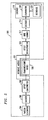
- FIG. 1 depicts a flow chart 100 illustrating steps of an exemplary method for generating an offset test pattern according to one aspect of the present invention.
- a frame can be generated at block 104.
- the frame can be encoded as at block 106.
- the frame can then be offset from the prior frame as at block 108. It will be appreciated that, for the first frame generated, there is no previous frame to be offset from, so no offset operation need be performed in such case.
- decision block 110 if there are additional frames to be generated for a given group of frames, the process can loop back to block 104.
- N the number of frames that are required. If such were the case, one would again loop back to block 104. For example, if it were desired to generate two groups of 4 frames each, after generating the first four frames as described above, one would pass from block 110 to block 112, determine that another group of N frames (in this case, 4) was required, and repeat the process for the four additional frames of the second group of four frames. If no additional groups of frames are required, one is done, as per block 114, but it will of course be realized that one can traverse through the method again when additional tests are desired.
- the predetermined amount by which a frame is offset from a preceding frame can be any amount that results in the piece of equipment under test being exposed to a desired pattern.
- the predetermined amount can be a number of bits equal to n-1, that is, each frame can be offset by one bit as compared to a preceding frame.
- the encoding step can be employed when necessary or desirable, depending on the type of equipment being tested and the applicable standard(s) that govern the equipment, its testing, and its operation. In the Fibre Channel standard mentioned above, 8b10b encoding can be employed. Test patterns according to other standards can be employed.
- such other standards can include SAS (serial attached SCSI (small computer system interface)), SATA (serial advanced technology attachment), PCIE (PCI (peripheral components interface) express), and RapidIO (RapidIO interconnect architecture as specified by the RapidIO Trade Association).
- SAS serial attached SCSI (small computer system interface)
- SATA serial advanced technology attachment
- PCIE PCI (peripheral components interface) express
- RapidIO RapidIO interconnect architecture as specified by the RapidIO Trade Association
- one aspect of the present invention allows the offsetting of frames to enhance diagnostic capabilities of a given test pattern.
- the receiver can be a stand alone unit, or can be associated with a unit having both transmit and receive capability.
- One exemplary application is to a serializer/deserializer (SerDes).
- SerDes serializer/deserializer
- the test pattern is depicted as the letters "TESTPAT” but the skilled artisan will appreciate that the test pattern will comprise one of a number of different possible bit sequences, depending on criteria such as what standard one is following. Further, the "TESTPAT” is shown, for illustrative convenience, encapsulated in a frame of alternating zeroes and ones.
- the frame may include any desired bit sequence; for example, in the aforementioned Fibre Channel standard, the test pattern is encapsulated into a frame including an SOP (start of packet) field, DATA (the test pattern), a CRC (cyclic redundancy check) field, an EOP (end of packet) field, and an IOS (idle ordered set).
- SOP start of packet
- DATA the test pattern
- CRC cyclic redundancy check
- EOP end of packet
- IOS Idle ordered set.
- Table A.11 of the Fibre Channel - Methodologies for Jitter and Signal Quality (FC-MJSQ) Specification Technical Report Rev. 10, of March 10, 2003 sets forth in detail the "Compliant Receive Jitter Tolerance Pattern" or "CJPAT" which is known to a person of ordinary skill in the communications art and which is one example of the type of pattern with which aspects of the present invention can be employed. It can be seen that "TESTPAT" is offset by one bit for each subsequent frame in the example shown in
- FIG. 3 the data pattern to which each of four latches receiving high speed serial input (labeled as Latch 1 through Latch 4 respectively) are exposed is depicted at four time steps numbered 302, 304, 306, and 308. If the offset process of the present invention was not employed, Latch 1 would always see the part of the pattern corresponding to the first "T” in “TESTPAT,” Latch 2 would always see the “E,” and so on. Note that Latch 4 "sees” first the second “T” in “TESTPAT,” then the “S,” then the "E,” and then the first "T.”
- FIG. 4 which is similar to FIG. 3 , for four time steps numbered 402, 404, 406, 408, but the alternating ones and zeroes in which the "TESTPAT" was encapsulated have been eliminated to show only the four letters “TEST”; it will be seen that each latch is exposed in each of the four time steps to each of the four different letters of "TEST," i.e., first "T,” “E,” “S,” and last “T.” (Each letter of course represents a corresponding part of a bit sequence of an actual pattern.) It will be appreciated that without the offset effect according to aspects of the present invention, each latch would "see” its own static pattern, different from the other latches, but the same over time with respect to itself.
- each latch can be exposed to the same pattern as the other latches (i.e., the latches "see” different portions of the pattern at a given time, but over time, each can be exposed to the full pattern).
- the test pattern may have a positive or negative starting disparity and may advantageously be sized small enough to fit on a laboratory BERTS (bit error rate test system). Note that when encoding and decoding are employed, the offsetting (and subsequent removal of the offset) is typically performed on the encoded data.
- FIG. 5 depicts an exemplary embodiment of an apparatus 500 for testing a communications device 502, according to an aspect of the present invention.
- the apparatus 500 can include a pattern generator 504 that is configured to generate a first group of N consecutive frames each containing a test pattern, and an offset constructor 508 coupled to the pattern generator 504.
- N should be greater than or equal to 2
- Apparatus 500 can optionally include an encoder 506 interposed between pattern generator 504 and offset constructor 508.
- Encoder 506 can be configured to receive the first and subsequent groups of N consecutive frames, to encode the frames to generate encoded frames, and to pass the encoded frames to the offset constructor 508.
- apparatus 500 can optionally include an offset deconstructor 510 that is configured to remove the offset from each of the offset frames, a byte aligner 512 that recognizes frame boundaries via special symbols (useful, for example, in Fibre Channel compliant physical link layer data paths), a decoder 514 (employed when encoder 506 is employed) to decode the encoded frames with the offset removed, and a checker 516 configured to compare the output of the offset deconstructor 510 (passed through the byte aligner 512 and/or decoder 514 as required for a given application) to a reference.
- an offset deconstructor 510 that is configured to remove the offset from each of the offset frames
- a byte aligner 512 that recognizes frame boundaries via special symbols (useful, for example, in Fibre Channel compliant physical link layer data paths)
- a decoder 514 employed when encoder 506 is employed
- a checker 516 configured to compare the output of the offset deconstructor 510 (passed through the byte aligner 512 and
- the checker 516 can include a comparator 518 (for example a compliant jitter test 10b synchronizer and checker) coupled to a reference 520 (for example an 8b10b reference encoder) for such purpose.
- Apparatus 500 can further include an interface module 522 configured to interconnect the communications device between the offset constructor 508 and the offset deconstructor 510.
- the elements 504 through 520 can be coupled as shown in FIG. 5 , and when optional elements are not used, adjacent elements can be coupled directly together.
- Module 522 can include, for example, appropriate connectors to establish electrical and/or optical interconnections to the device 502 to be tested.
- Device 502 can be any type of device, apparatus, discrete circuit, component, integrated circuit, hybrid circuit, or the like that can benefit from diagnosis with the offset test pattern.
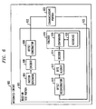
- Circuit 600 can include a communications portion 602 and a built-in test portion 603.
- the communications portion 602 can include any kind of communications functionality typically implemented on an integrated circuit; for example, a receiver, receiver functionality of a transmitter/receiver, or a serializer/deserializer with multiple receiver latches.
- the built-in test portion can include one or more of elements numbered 604 through 620 similar to elements 504 through 520 described with respect to FIG. 5 .
- the communications portion 602 can be interconnected between offset constructor 608 and offset deconstructor 610 via an interface portion; for example, by appropriate interconnections formed on integrated circuit chip 600 and suggested by arrows 622.
- the interface portion can, if desired, be configured to selectively interconnect communications portion 602 to test portion 603 for periodic self test and/or other diagnostic functions.
- test patterns can be generated, for example, lookup tables or appropriately configured shift registers.
- At least a portion of the techniques of the present invention described herein may be implemented in an integrated circuit.
- a plurality of identical die are typically fabricated in a repeated pattern on a surface on a semi-conductor wafer.
- Each die can include an entire circuit or elements as described herein, and can include other structures or circuits.
- the individual die are cut or diced from the wafer, and then packaged as an integrated circuit.
- One skilled in the art will know how to dice wafers and package die to produce integrated circuits.
Landscapes
- Engineering & Computer Science (AREA)
- Computer Networks & Wireless Communication (AREA)
- Signal Processing (AREA)
- Maintenance And Management Of Digital Transmission (AREA)
- Tests Of Electronic Circuits (AREA)
Description
- The present invention relates generally to communications equipment, and more particularly relates to an apparatus and method for generating an offset test pattern for testing such equipment.
- Communications equipment must typically be tested in order to verify proper performance. Such testing can include, for example, development testing, wherein proper functioning of a prototype of a candidate design is verified; acceptance testing, where it is confirmed that an individual component or piece of equipment functions according to specifications; or ongoing field tests, where correct functioning of equipment in the field is monitored. Such testing may be performed, for example, by external test equipment or by built-in self-test (BIST) capability.
- One manner of testing communications equipment is to subject the equipment to test patterns that simulate the type of data that the equipment will be handling in use. For example, Fibre Channel Framing and Signalling draft standard FC-FS Rev. 1.80 is a proposed American National Standard for Information Technology. A Fibre Channel jitter tolerance pattern formed by framing an 8b10b encoded random jitter test pattern into a standard frame can be employed with respect to applications of the aforementioned standard. Some types of communications equipment, for example, serializer/deserializers, may have multiple receiver latches. If conventional test techniques are employed with such equipment, each latch may only be exposed to a static pattern, and thus only static mono failure of the given latch may be detected.
-
U.S. 5,392,314 discloses a process for determining quality parameters of a transmission link for digital data streams. The digital data streams have a cellular structure, each cell having a useful field able to be freely occupied with data. In the process, a sequence of test cells is provided as a test signal. The useful fields of the test cells are partially occupied, in each case, with a test pattern. The test pattern consists of a number of binary-coded data wherein the auto-correlation function of the test pattern roughly corresponds to a Dirac pulse. The position of the test pattern within the useful fields of the test cells is shifted within the series of test cells such that the position of the test pattern within the useful filed is not repeated in the sequence. The series of test cells is then transmitted through the transmission link. After being transmitted through the transmission link, each cell of the data stream is correlated with a reference pattern. The reference pattern is either identical to the test pattern or to the inverse of the test pattern. Lastly, the maximum of the obtained cross-correlation function is evaluated with respect to its position relative to the start of the particular cell and with respect to its height. In each of the test cells, additional test pattern(s) may be provided in a section of the useful field separate from the section of the useful field containing the original test pattern. - Accordingly, it would be desirable to provide an apparatus and method where test patterns can be offset in successive frames, such that more failure modes can be detected than with a test technique where offset is not employed, for equipment having multiple receiver latches, and other equipment that can benefit from pattern offset.
- In accordance with one aspect the invention provides a method according to
claim 1. In accordance with another aspect the invention provides an apparatus according to claim 5. In accordance with a further aspect the invention provides an integrated circuit according to claim 8. - An illustrative method for generating an offset test pattern, according to one aspect of the invention, can include the steps of generating a first group of N consecutive frames each containing a test pattern, where N is greater than or equal to 2 and the N consecutive frames are numbered n=1, 2, ..., N; and offsetting each of the frames numbered n=2 through N by a predetermined amount relative to the first frame, to enhance diagnostic capabilities of the test pattern.
- In another aspect, one exemplary embodiment of an apparatus for testing a communications device can include a pattern generator that is configured to generate a first group of N consecutive frames each containing a test pattern of the kind just described, and an offset constructor coupled to the pattern generator. The offset constructor can be configured to offset frames as described in the preceding paragraph.
- In yet another aspect, an apparatus according to another exemplary embodiment of the present invention can be configured to provide BIST capability to a communications circuit, device, or component, such as, for example, an integrated circuit.
- A more complete understanding of the present invention, as well as further features and advantages of the present invention, will be obtained by reference to the following detailed description and drawings.
-
-
FIG. 1 is a flow chart depicting exemplary method steps for generating an offset test pattern in accordance with an aspect of the present invention; -
FIG. 2 depicts an exemplary offset test pattern in two groups of four frames each; -
FIG. 3 depicts four latches of a receiver receiving the offset test pattern ofFIG. 2 as high speed serial input; -
FIG. 4 depicts the effective test pattern to which the four latches ofFIG. 3 are exposed to over time; -
FIG. 5 depicts an exemplary embodiment of an apparatus for testing a communications device according to an aspect of the present invention; and -
FIG. 6 depicts an exemplary integrated circuit having BIST capability according to another aspect of the present invention. - Reference should now be had to
FIG. 1 , which depicts aflow chart 100 illustrating steps of an exemplary method for generating an offset test pattern according to one aspect of the present invention. The method can include the steps of generating a first group of N consecutive frames each containing a test pattern, where N≥2, the N consecutive frames being numbered n=1, 2, ..., N; and offsetting each of the frames numbered n=2 through N by a predetermined amount relative to the frame numbered n=1, to enhance diagnostic capabilities of the test pattern. For example, as shown inflow chart 100, after starting atblock 102, a frame can be generated atblock 104. Optionally, the frame can be encoded as atblock 106. The frame can then be offset from the prior frame as atblock 108. It will be appreciated that, for the first frame generated, there is no previous frame to be offset from, so no offset operation need be performed in such case. - As shown at
decision block 110, if there are additional frames to be generated for a given group of frames, the process can loop back toblock 104. Thus, by way of example, if N=4, one would traverseblocks 104, 106 (optionally), and 108 initially, and then repeat three times until all four frames had been generated. As indicated atdecision block 112, one could then determine if additional groups of frames were required. If such were the case, one would again loop back toblock 104. For example, if it were desired to generate two groups of 4 frames each, after generating the first four frames as described above, one would pass fromblock 110 toblock 112, determine that another group of N frames (in this case, 4) was required, and repeat the process for the four additional frames of the second group of four frames. If no additional groups of frames are required, one is done, as perblock 114, but it will of course be realized that one can traverse through the method again when additional tests are desired. - The predetermined amount by which a frame is offset from a preceding frame can be any amount that results in the piece of equipment under test being exposed to a desired pattern. In a typical case, the predetermined amount can be a number of bits equal to n-1, that is, each frame can be offset by one bit as compared to a preceding frame. The encoding step can be employed when necessary or desirable, depending on the type of equipment being tested and the applicable standard(s) that govern the equipment, its testing, and its operation. In the Fibre Channel standard mentioned above, 8b10b encoding can be employed. Test patterns according to other standards can be employed. By way of example and not limitation, such other standards can include SAS (serial attached SCSI (small computer system interface)), SATA (serial advanced technology attachment), PCIE (PCI (peripheral components interface) express), and RapidIO (RapidIO interconnect architecture as specified by the RapidIO Trade Association).
- As noted, one aspect of the present invention allows the offsetting of frames to enhance diagnostic capabilities of a given test pattern. By way of example, one type of equipment that can benefit from such offsetting is a receiver having two or more latches numbered m=1, 2, ..., M; such latches can be, e.g., high speed data latches operating at frequencies on the order of GHz. The receiver can be a stand alone unit, or can be associated with a unit having both transmit and receive capability. One exemplary application is to a serializer/deserializer (SerDes). In such a case, the number of frames N in a group of frames undergoing the offset process should be greater than or equal to, and an integer multiple of, M:


where i is an integer greater than or equal to 1. - Attention should now be given to
FIG. 2 , which shows twogroups FIG. 2 . - Turning now to
FIG. 3 , the data pattern to which each of four latches receiving high speed serial input (labeled asLatch 1 throughLatch 4 respectively) are exposed is depicted at four time steps numbered 302, 304, 306, and 308. If the offset process of the present invention was not employed,Latch 1 would always see the part of the pattern corresponding to the first "T" in "TESTPAT,"Latch 2 would always see the "E," and so on. Note thatLatch 4 "sees" first the second "T" in "TESTPAT," then the "S," then the "E," and then the first "T." - The effect over time of the phenomena discussed in the preceding paragraph is best appreciated by viewing
FIG. 4 , which is similar toFIG. 3 , for four time steps numbered 402, 404, 406, 408, but the alternating ones and zeroes in which the "TESTPAT" was encapsulated have been eliminated to show only the four letters "TEST"; it will be seen that each latch is exposed in each of the four time steps to each of the four different letters of "TEST," i.e., first "T," "E," "S," and last "T." (Each letter of course represents a corresponding part of a bit sequence of an actual pattern.) It will be appreciated that without the offset effect according to aspects of the present invention, each latch would "see" its own static pattern, different from the other latches, but the same over time with respect to itself. With the offset effect according to aspects of the present invention, over time each latch can be exposed to the same pattern as the other latches (i.e., the latches "see" different portions of the pattern at a given time, but over time, each can be exposed to the full pattern). It should be noted that the test pattern may have a positive or negative starting disparity and may advantageously be sized small enough to fit on a laboratory BERTS (bit error rate test system). Note that when encoding and decoding are employed, the offsetting (and subsequent removal of the offset) is typically performed on the encoded data. - Attention should now be given to
FIG. 5 , which depicts an exemplary embodiment of anapparatus 500 for testing acommunications device 502, according to an aspect of the present invention. Theapparatus 500 can include apattern generator 504 that is configured to generate a first group of N consecutive frames each containing a test pattern, and an offsetconstructor 508 coupled to thepattern generator 504. As discussed above with regard to an exemplary method, N should be greater than or equal to 2, and the N consecutive frames can be numbered n=1, 2, ..., N. The said offsetconstructor 508 can be configured to offset each of the frames numbered n=2 through N by a predetermined amount relative to the frame numbered n=1, to enhance diagnostic capabilities of the test pattern, as previously discussed. -
Apparatus 500 can optionally include anencoder 506 interposed betweenpattern generator 504 and offsetconstructor 508.Encoder 506 can be configured to receive the first and subsequent groups of N consecutive frames, to encode the frames to generate encoded frames, and to pass the encoded frames to the offsetconstructor 508. Further,apparatus 500 can optionally include an offsetdeconstructor 510 that is configured to remove the offset from each of the offset frames, abyte aligner 512 that recognizes frame boundaries via special symbols (useful, for example, in Fibre Channel compliant physical link layer data paths), a decoder 514 (employed whenencoder 506 is employed) to decode the encoded frames with the offset removed, and achecker 516 configured to compare the output of the offset deconstructor 510 (passed through thebyte aligner 512 and/ordecoder 514 as required for a given application) to a reference. Thechecker 516 can include a comparator 518 (for example a compliant jitter test 10b synchronizer and checker) coupled to a reference 520 (for example an 8b10b reference encoder) for such purpose.Apparatus 500 can further include aninterface module 522 configured to interconnect the communications device between the offsetconstructor 508 and the offsetdeconstructor 510. Theelements 504 through 520 can be coupled as shown inFIG. 5 , and when optional elements are not used, adjacent elements can be coupled directly together.Module 522 can include, for example, appropriate connectors to establish electrical and/or optical interconnections to thedevice 502 to be tested.Device 502 can be any type of device, apparatus, discrete circuit, component, integrated circuit, hybrid circuit, or the like that can benefit from diagnosis with the offset test pattern. - Reference should now be had to
FIG. 6 , which shows an exemplary embodiment of anintegrated circuit 600, for communications applications, in accordance with another aspect of the present invention.Circuit 600 can include acommunications portion 602 and a built-intest portion 603. Thecommunications portion 602 can include any kind of communications functionality typically implemented on an integrated circuit; for example, a receiver, receiver functionality of a transmitter/receiver, or a serializer/deserializer with multiple receiver latches. The built-in test portion can include one or more of elements numbered 604 through 620 similar toelements 504 through 520 described with respect toFIG. 5 . Thecommunications portion 602 can be interconnected between offsetconstructor 608 and offsetdeconstructor 610 via an interface portion; for example, by appropriate interconnections formed onintegrated circuit chip 600 and suggested byarrows 622. The interface portion can, if desired, be configured to selectively interconnectcommunications portion 602 to testportion 603 for periodic self test and/or other diagnostic functions. - Different aspects and embodiments of the present invention can be implemented, for example, in dedicated hardware, hardware with application specific firmware, software, or a combination thereof; and the test patterns can be generated, for example, lookup tables or appropriately configured shift registers.
- At least a portion of the techniques of the present invention described herein may be implemented in an integrated circuit. In forming integrated circuits, a plurality of identical die are typically fabricated in a repeated pattern on a surface on a semi-conductor wafer. Each die can include an entire circuit or elements as described herein, and can include other structures or circuits. The individual die are cut or diced from the wafer, and then packaged as an integrated circuit. One skilled in the art will know how to dice wafers and package die to produce integrated circuits.
- Although illustrative embodiments of the present invention have been described herein, it is to be understood that the invention is not limited to those precise embodiments, and that various other changes and modifications may be made by one skilled in the art without departing from the scope of the invention as set forth in the appended claims.
Claims (8)
- A method for generating an offset test pattern and testing a receiver, comprising the steps of:generating (104) a first group of N consecutive frames (202) each containing a test pattern, where N≥2, said N consecutive frames being numbered n=1, 2, ..., N;offsetting (108) each test pattern contained in said frames numbered n=2 through N by a predetermined amount relative to said frame numbered n=1, to enhance diagnostic capabilities of the test pattern; andtesting said receiver having M receiver latches numbered m=1, 2, ..., M, M≥2, by exposing said receiver to said offset test pattern, wherein N≥M;said method characterized by:said predetermined amount is given by a number of bits equal to n-1; andN=iM where i is an integer ≥ 1.
- The method of claim 1, further comprising the additional steps of:generating subsequent groups ofN consecutive frames; andoffsetting each frame in said subsequent groups by one bit relative to a preceding frame.
- The method of claim 2, further comprising the additional steps of encoding said first and subsequent groups ofN consecutive frames.
- The method of claim 3, wherein said encoding comprises 8b/10b encoding and the test pattern comprises a standard jitter test pattern corresponding to at least one of a fibre channel standard, a SAS [serial attached SCSI [small computer system interface]] standard, a SATA [serial advanced technology attachment] standard, a PCIE [PCI [peripheral components interface] express] standard, and a RapidIO [RapidIO interconnect architecture as specified by the RapidIO Trade Association] standard.
- An apparatus for generating an offset test pattern and testing a communications device, comprising:a pattern generator (504) that is configured to generate a first group of N consecutive frames each containing a test pattern, where N≥2, said N consecutive frames being numbered n=1,2, ..., N; andan offset constructor (508) coupled to said pattern generator, said offset constructor being configured to offset each test pattern contained in said frames numbered n=2 through N by a predetermined amount relative to said frame numbered n=1 to enhance diagnostic capabilities of the test pattern, said diagnostic capabilities of the test pattern are enhanced for testing of a receiver having M receiver latches numbered m=1, 2, ..., M, K≥2, wherein N≥M;characterized by:said predetermined amount is given by a number of bits equal to n-1; andN=iM where i is an integer ≥ 1.
- The apparatus of claim 5, further comprising:an offset deconstructor configured to remove said offset from each of said frames numbered n=2 through N;a checker configured to compare output of said offset deconstructor to a reference; andan interface module configured to interconnect the communications device between said offset constructor and said offset deconstructor.
- The apparatus of claim 6, further comprising:an encoder interposed between said pattern generator and said offset constructor, said encoder being configured to receive said first and subsequent groups of N consecutive frames, to encode said frames, thereby generating encoded frames, and to pass said encoded frames to said offset constructor; anda decoder interposed between said offset deconstructor and said checker, said decoder being configured to receive, from said offset deconstructor, said encoded frames numbered n=2 through N with said offset removed, and to decode said encoded frames;wherein said offset constructor is configured to offset said encoded frames and said offset deconstructor is configured to remove said offset from said encoded frames.
- An integrated circuit for communications applications, with built-in test capability to generate an offset test pattern and test a device, said integrated circuit comprising:a communications portion, wherein said communications portion comprises a receiver having M receiver latches numbered m=1, 2, ..., M, M≥2; anda built-in test portion, said built-in test portion in turn comprising:characterized by:a pattern generator that is configured to generate a first group of N consecutive frames each containing a test pattern, where N≥2, said N consecutive frames being numbered n=1, 2, ..., N, wherein N≥M;an offset constructor coupled to said pattern generator, said offset constructor being configured to offset each test pattern contained in said frames numbered n=2 through N by a predetermined amount relative to said frame numbered n=1, to enhance diagnostic capabilities of the test pattern;an offset deconstructor configured to remove said offset from each of said frames numbered n=2 through N;a checker configured to compare output of said offset deconstructor to a reference; andan interface portion configured to interconnect said communications portion between said offset constructor and said offset deconstructor;said predetermined amount is given by a number of bits equal to n-1; andN=iM where i is an integer ≥ 1.
Applications Claiming Priority (1)
| Application Number | Priority Date | Filing Date | Title |
|---|---|---|---|
| US11/121,164 US7447965B2 (en) | 2005-05-03 | 2005-05-03 | Offset test pattern apparatus and method |
Publications (2)
| Publication Number | Publication Date |
|---|---|
| EP1720280A1 EP1720280A1 (en) | 2006-11-08 |
| EP1720280B1 true EP1720280B1 (en) | 2012-07-18 |
Family
ID=36297963
Family Applications (1)
| Application Number | Title | Priority Date | Filing Date |
|---|---|---|---|
| EP06251266A Ceased EP1720280B1 (en) | 2005-05-03 | 2006-03-09 | Offset test pattern apparatus and method |
Country Status (3)
| Country | Link |
|---|---|
| US (1) | US7447965B2 (en) |
| EP (1) | EP1720280B1 (en) |
| JP (1) | JP5536298B2 (en) |
Families Citing this family (11)
| Publication number | Priority date | Publication date | Assignee | Title |
|---|---|---|---|---|
| US7930377B2 (en) | 2004-04-23 | 2011-04-19 | Qlogic, Corporation | Method and system for using boot servers in networks |
| US7340167B2 (en) | 2004-04-23 | 2008-03-04 | Qlogic, Corporation | Fibre channel transparent switch for mixed switch fabrics |
| US7669190B2 (en) * | 2004-05-18 | 2010-02-23 | Qlogic, Corporation | Method and system for efficiently recording processor events in host bus adapters |
| US7577772B2 (en) | 2004-09-08 | 2009-08-18 | Qlogic, Corporation | Method and system for optimizing DMA channel selection |
| US20060064531A1 (en) * | 2004-09-23 | 2006-03-23 | Alston Jerald K | Method and system for optimizing data transfer in networks |
| US7676611B2 (en) | 2004-10-01 | 2010-03-09 | Qlogic, Corporation | Method and system for processing out of orders frames |
| US7392437B2 (en) * | 2005-01-20 | 2008-06-24 | Qlogic, Corporation | Method and system for testing host bus adapters |
| US20070104219A1 (en) * | 2005-11-09 | 2007-05-10 | Honeywell International Inc. | System and method to facilitate testing of rapidio components |
| DE102010020772A1 (en) * | 2010-05-17 | 2011-11-17 | Adva Ag Optical Networking | Method for transmitting a digital signal in inverse multiplex, in particular via an optical transport network and receiving device for a system for implementing the method |
| JP5832800B2 (en) * | 2011-07-13 | 2015-12-16 | 株式会社メガチップス | Semiconductor integrated circuit and test method for semiconductor integrated circuit |
| US11301411B2 (en) * | 2019-06-07 | 2022-04-12 | Intel Corporation | Data structures for refined link training |
Family Cites Families (39)
| Publication number | Priority date | Publication date | Assignee | Title |
|---|---|---|---|---|
| EP0389697B1 (en) * | 1989-03-29 | 1994-11-02 | International Business Machines Corporation | Serial data receiver |
| DE3912660C1 (en) * | 1989-04-18 | 1990-08-30 | Wandel & Goltermann Gmbh & Co, 7412 Eningen, De | |
| DE4014766A1 (en) * | 1990-04-19 | 1992-01-09 | Siemens Ag | METHOD FOR DETERMINING QUALITY PARAMETERS OF A TRANSMISSION RANGE FOR DIGITAL DATA FLOWS WITH CELL STRUCTURE |
| DE69114183T2 (en) * | 1990-06-07 | 1996-05-30 | Ibm | System for the reduction of test data memories. |
| US5282211A (en) * | 1991-08-14 | 1994-01-25 | Genrad, Inc. | Slip detection during bit-error-rate measurement |
| US5726991A (en) * | 1993-06-07 | 1998-03-10 | At&T Global Information Solutions Company | Integral bit error rate test system for serial data communication links |
| US6032282A (en) * | 1994-09-19 | 2000-02-29 | Advantest Corp. | Timing edge forming circuit for IC test system |
| US5592674A (en) * | 1994-12-20 | 1997-01-07 | International Business Machines Corporation | Automatic verification of external interrupts |
| JP3609205B2 (en) * | 1996-06-14 | 2005-01-12 | 株式会社東芝 | Mobile communication device and its AFC initial value setting method |
| US6498929B1 (en) * | 1996-06-21 | 2002-12-24 | Kabushiki Kaisha Toshiba | Receiver having DC offset decreasing function and communication system using the same |
| JP3316623B2 (en) * | 1998-01-29 | 2002-08-19 | 新家工業株式会社 | Spoke insertion device |
| US6201829B1 (en) * | 1998-04-03 | 2001-03-13 | Adaptec, Inc. | Serial/parallel GHZ transceiver with pseudo-random built in self test pattern generator |
| JP3428965B2 (en) * | 1998-12-01 | 2003-07-22 | サムスン エレクトロニクス カンパニー リミテッド | Frequency synchronizer for orthogonal frequency division multiplexing / code division multiple access system |
| US6363060B1 (en) * | 1999-06-30 | 2002-03-26 | Qualcomm Incorporated | Method and apparatus for fast WCDMA acquisition |
| US6553529B1 (en) * | 1999-07-23 | 2003-04-22 | Teradyne, Inc. | Low cost timing system for highly accurate multi-modal semiconductor testing |
| US6834367B2 (en) * | 1999-12-22 | 2004-12-21 | International Business Machines Corporation | Built-in self test system and method for high speed clock and data recovery circuit |
| AU2001227892A1 (en) * | 2000-01-14 | 2001-07-24 | Parthus Technologies Plc | An algorithmic test pattern generator, with built-in-self-test (bist) capabilities, for functional testing of a circuit |
| US6684350B1 (en) * | 2000-12-22 | 2004-01-27 | Cisco Technology, Inc. | Repetitive pattern testing circuit for AC-coupled systems |
| US7042842B2 (en) * | 2001-06-13 | 2006-05-09 | Computer Network Technology Corporation | Fiber channel switch |
| US6977960B2 (en) * | 2001-08-16 | 2005-12-20 | Matsushita Electric Industrial Co., Ltd. | Self test circuit for evaluating a high-speed serial interface |
| US20040052521A1 (en) * | 2002-04-12 | 2004-03-18 | Ross Halgren | Diagnostic monitoring system for WDM networks |
| US6973603B2 (en) * | 2002-06-28 | 2005-12-06 | Intel Corporation | Method and apparatus for optimizing timing for a multi-drop bus |
| US6865660B2 (en) * | 2002-06-28 | 2005-03-08 | Micron Technology, Inc. | Method and apparatus for generating deterministic, non-repeating, pseudo-random addresses |
| US20040015761A1 (en) * | 2002-07-22 | 2004-01-22 | Finisar Corporation | Scalable asynchronous I/O testing tool |
| US7093172B2 (en) * | 2002-08-07 | 2006-08-15 | Broadcom Corporation | System and method for determining on-chip bit error rate (BER) in a communication system |
| JP2004096427A (en) * | 2002-08-30 | 2004-03-25 | Kyushu Ando Denki Kk | Pattern generating apparatus and method |
| JP4425537B2 (en) * | 2002-10-01 | 2010-03-03 | 株式会社アドバンテスト | Test apparatus and test method |
| US7111208B2 (en) * | 2002-10-02 | 2006-09-19 | Broadcom Corporation | On-chip standalone self-test system and method |
| US6968490B2 (en) * | 2003-03-07 | 2005-11-22 | Intel Corporation | Techniques for automatic eye-degradation testing of a high-speed serial receiver |
| EP1654548A1 (en) | 2003-08-06 | 2006-05-10 | Agilent Technologies, Inc. | Digital data signal testing using arbitrary test signal |
| US7275195B2 (en) * | 2003-10-03 | 2007-09-25 | Avago Technologies General Ip (Singapore) Pte. Ltd. | Programmable built-in self-test circuit for serializer/deserializer circuits and method |
| US20050086563A1 (en) * | 2003-10-16 | 2005-04-21 | International Business Machines Corporation | Channel-based testing of communication link |
| US7444559B2 (en) * | 2004-01-28 | 2008-10-28 | Micron Technology, Inc. | Generation of memory test patterns for DLL calibration |
| US7533285B2 (en) * | 2004-04-22 | 2009-05-12 | Hewlett-Packard Development Company, L.P. | Synchronizing link delay measurement over serial links |
| US20050270870A1 (en) * | 2004-06-02 | 2005-12-08 | Sangho Shin | Time slot interchange switch with cache |
| JP4261432B2 (en) * | 2004-07-09 | 2009-04-30 | 株式会社アドバンテスト | Semiconductor test apparatus and semiconductor test method |
| US7595629B2 (en) * | 2004-07-09 | 2009-09-29 | Formfactor, Inc. | Method and apparatus for calibrating and/or deskewing communications channels |
| WO2006055862A2 (en) * | 2004-11-18 | 2006-05-26 | Mentor Graphics Corporation | Programmable memory built-in-self-test (mbist) method and apparatus |
| US7272767B2 (en) * | 2005-04-29 | 2007-09-18 | Freescale Semiconductor, Inc. | Methods and apparatus for incorporating IDDQ testing into logic BIST |
-
2005
- 2005-05-03 US US11/121,164 patent/US7447965B2/en not_active Expired - Fee Related
-
2006
- 2006-03-09 EP EP06251266A patent/EP1720280B1/en not_active Ceased
- 2006-05-02 JP JP2006128043A patent/JP5536298B2/en not_active Expired - Fee Related
Also Published As
| Publication number | Publication date |
|---|---|
| JP5536298B2 (en) | 2014-07-02 |
| EP1720280A1 (en) | 2006-11-08 |
| JP2006313159A (en) | 2006-11-16 |
| US7447965B2 (en) | 2008-11-04 |
| US20060253757A1 (en) | 2006-11-09 |
Similar Documents
| Publication | Publication Date | Title |
|---|---|---|
| TWI307462B (en) | Ibist apparatus and computer system | |
| JP5624781B2 (en) | COMMUNICATION SYSTEM, DATA TRANSMITTING DEVICE, AND DATA RECEIVING DEVICE | |
| US7984369B2 (en) | Concurrent code checker and hardware efficient high-speed I/O having built-in self-test and debug features | |
| JP5697833B2 (en) | Interface test circuit and method | |
| US8990653B2 (en) | Apparatus and method for transmitting and recovering encoded data streams across multiple physical medium attachments | |
| CN101127650B (en) | Method and test backplane for single board production test | |
| CN1054344A (en) | The detection method of Frame Alignment Word and equipment in the data flow | |
| EP0996262A1 (en) | Communication system with plurality of synchronised data links | |
| US7272756B2 (en) | Exploitive test pattern apparatus and method | |
| US7447965B2 (en) | Offset test pattern apparatus and method | |
| US20070168835A1 (en) | Serial communications system and method | |
| CN100417062C (en) | A bit error detection method and device for a wireless digital communication system | |
| KR101423328B1 (en) | Concurrent code checker and hardware efficient high-speed i/o having built-in self-test and debug features | |
| US7251304B2 (en) | Bit synchronizing circuit configured to obviate errors from meta-stability | |
| JP2009164833A (en) | Data processing apparatus and method, and program | |
| EP3731106B1 (en) | Data transmission code and interface | |
| US11438109B2 (en) | Apparatuses and methods to change information values | |
| CN117120856A (en) | A chip testing circuit and method | |
| CN118227545A (en) | Low-voltage differential signal self-training transmission device, platform and application method | |
| CN117856986A (en) | Circuit system design applied to bit error rate test | |
| US7075461B2 (en) | Method of generating pseudo 8B/10B code and apparatus for generating the same | |
| US20040193975A1 (en) | Method and an apparatus for transmit phase select | |
| US12381579B2 (en) | Error rate measurement apparatus and error rate measurement method | |
| US12381576B2 (en) | Error rate measurement apparatus and error rate measurement method | |
| CN111651311B (en) | A configurable physical layer error generation device, chip and equipment |
Legal Events
| Date | Code | Title | Description |
|---|---|---|---|
| PUAI | Public reference made under article 153(3) epc to a published international application that has entered the european phase |
Free format text: ORIGINAL CODE: 0009012 |
|
| AK | Designated contracting states |
Kind code of ref document: A1 Designated state(s): AT BE BG CH CY CZ DE DK EE ES FI FR GB GR HU IE IS IT LI LT LU LV MC NL PL PT RO SE SI SK TR |
|
| AX | Request for extension of the european patent |
Extension state: AL BA HR MK YU |
|
| RIN1 | Information on inventor provided before grant (corrected) |
Inventor name: SMITH, LANE A. Inventor name: OLSEN, MAX J. Inventor name: SCHIESSLER, GARY E. Inventor name: BRINK, ROBERT D. Inventor name: HOFMANN, JR. , JAMES WALTER |
|
| RIN1 | Information on inventor provided before grant (corrected) |
Inventor name: HOFMANN, JR. , JAMES WALTER Inventor name: BRINK, ROBERT D. Inventor name: SMITH, LANE A. Inventor name: SCHIESSLER, GARY E. Inventor name: OLSEN, MAX J. |
|
| 17P | Request for examination filed |
Effective date: 20070504 |
|
| 17Q | First examination report despatched |
Effective date: 20070604 |
|
| AKX | Designation fees paid |
Designated state(s): DE GB |
|
| GRAP | Despatch of communication of intention to grant a patent |
Free format text: ORIGINAL CODE: EPIDOSNIGR1 |
|
| GRAS | Grant fee paid |
Free format text: ORIGINAL CODE: EPIDOSNIGR3 |
|
| GRAA | (expected) grant |
Free format text: ORIGINAL CODE: 0009210 |
|
| AK | Designated contracting states |
Kind code of ref document: B1 Designated state(s): DE GB |
|
| REG | Reference to a national code |
Ref country code: GB Ref legal event code: FG4D |
|
| REG | Reference to a national code |
Ref country code: DE Ref legal event code: R096 Ref document number: 602006030819 Country of ref document: DE Effective date: 20120913 |
|
| PLBE | No opposition filed within time limit |
Free format text: ORIGINAL CODE: 0009261 |
|
| STAA | Information on the status of an ep patent application or granted ep patent |
Free format text: STATUS: NO OPPOSITION FILED WITHIN TIME LIMIT |
|
| 26N | No opposition filed |
Effective date: 20130419 |
|
| REG | Reference to a national code |
Ref country code: DE Ref legal event code: R097 Ref document number: 602006030819 Country of ref document: DE Effective date: 20130419 |
|
| PGFP | Annual fee paid to national office [announced via postgrant information from national office to epo] |
Ref country code: GB Payment date: 20140305 Year of fee payment: 9 |
|
| PGFP | Annual fee paid to national office [announced via postgrant information from national office to epo] |
Ref country code: DE Payment date: 20140417 Year of fee payment: 9 |
|
| REG | Reference to a national code |
Ref country code: DE Ref legal event code: R119 Ref document number: 602006030819 Country of ref document: DE |
|
| GBPC | Gb: european patent ceased through non-payment of renewal fee |
Effective date: 20150309 |
|
| PG25 | Lapsed in a contracting state [announced via postgrant information from national office to epo] |
Ref country code: DE Free format text: LAPSE BECAUSE OF NON-PAYMENT OF DUE FEES Effective date: 20151001 Ref country code: GB Free format text: LAPSE BECAUSE OF NON-PAYMENT OF DUE FEES Effective date: 20150309 |