EP1720230B1 - Power supply with current sensing circuit - Google Patents
Power supply with current sensing circuit Download PDFInfo
- Publication number
- EP1720230B1 EP1720230B1 EP06252367A EP06252367A EP1720230B1 EP 1720230 B1 EP1720230 B1 EP 1720230B1 EP 06252367 A EP06252367 A EP 06252367A EP 06252367 A EP06252367 A EP 06252367A EP 1720230 B1 EP1720230 B1 EP 1720230B1
- Authority
- EP
- European Patent Office
- Prior art keywords
- current sense
- current
- coupled
- sense circuit
- led
- Prior art date
- Legal status (The legal status is an assumption and is not a legal conclusion. Google has not performed a legal analysis and makes no representation as to the accuracy of the status listed.)
- Not-in-force
Links
- 230000001105 regulatory effect Effects 0.000 claims description 5
- 230000007704 transition Effects 0.000 claims description 2
- 238000000034 method Methods 0.000 description 7
- 230000008901 benefit Effects 0.000 description 5
- 238000004519 manufacturing process Methods 0.000 description 5
- 230000001052 transient effect Effects 0.000 description 5
- 230000015556 catabolic process Effects 0.000 description 3
- 230000008878 coupling Effects 0.000 description 3
- 238000010168 coupling process Methods 0.000 description 3
- 238000005859 coupling reaction Methods 0.000 description 3
- 239000003990 capacitor Substances 0.000 description 2
- 239000004065 semiconductor Substances 0.000 description 2
- 238000004804 winding Methods 0.000 description 2
- 238000004364 calculation method Methods 0.000 description 1
- 230000002860 competitive effect Effects 0.000 description 1
- 230000000295 complement effect Effects 0.000 description 1
- 238000010586 diagram Methods 0.000 description 1
- 230000000694 effects Effects 0.000 description 1
- 238000005516 engineering process Methods 0.000 description 1
- 230000010354 integration Effects 0.000 description 1
- 238000012986 modification Methods 0.000 description 1
- 230000004048 modification Effects 0.000 description 1
- 230000003287 optical effect Effects 0.000 description 1
- 230000009291 secondary effect Effects 0.000 description 1
- 230000008646 thermal stress Effects 0.000 description 1
- 238000009966 trimming Methods 0.000 description 1
- 230000000007 visual effect Effects 0.000 description 1
Images


Classifications
-
- G—PHYSICS
- G01—MEASURING; TESTING
- G01R—MEASURING ELECTRIC VARIABLES; MEASURING MAGNETIC VARIABLES
- G01R19/00—Arrangements for measuring currents or voltages or for indicating presence or sign thereof
- G01R19/165—Indicating that current or voltage is either above or below a predetermined value or within or outside a predetermined range of values
- G01R19/16533—Indicating that current or voltage is either above or below a predetermined value or within or outside a predetermined range of values characterised by the application
- G01R19/16538—Indicating that current or voltage is either above or below a predetermined value or within or outside a predetermined range of values characterised by the application in AC or DC supplies
- G01R19/16552—Indicating that current or voltage is either above or below a predetermined value or within or outside a predetermined range of values characterised by the application in AC or DC supplies in I.C. power supplies
-
- H—ELECTRICITY
- H02—GENERATION; CONVERSION OR DISTRIBUTION OF ELECTRIC POWER
- H02J—CIRCUIT ARRANGEMENTS OR SYSTEMS FOR SUPPLYING OR DISTRIBUTING ELECTRIC POWER; SYSTEMS FOR STORING ELECTRIC ENERGY
- H02J5/00—Circuit arrangements for transfer of electric power between AC networks and DC networks
-
- H—ELECTRICITY
- H02—GENERATION; CONVERSION OR DISTRIBUTION OF ELECTRIC POWER
- H02J—CIRCUIT ARRANGEMENTS OR SYSTEMS FOR SUPPLYING OR DISTRIBUTING ELECTRIC POWER; SYSTEMS FOR STORING ELECTRIC ENERGY
- H02J7/00—Circuit arrangements for charging or depolarising batteries or for supplying loads from batteries
- H02J7/02—Circuit arrangements for charging or depolarising batteries or for supplying loads from batteries for charging batteries from AC mains by converters
Definitions
- the present invention relates generally to electronic circuits, and more specifically, the invention relates to a current sense circuit.
- EP-A-1,278,070 discloses a current sense circuit as defined in the precharacterising portion of claim 1, in which the current sense voltage threshold is set by a difference between the forward voltage of an LED and a PN junction diode.
- Figure 1 shows an example of a low cost AC to DC CV/CC charger power supply.
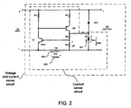
- Figure 2 shows an example of a current and voltage sense circuit with reduced current sense voltage threshold for an embodiment in accordance with the teachings of the present invention.
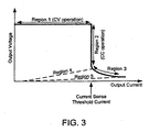
- Figure 3 is a diagram illustrating various operating regions in the output characteristics of a CV/CC charger power supply for an embodiment in accordance with the teachings of the present invention.
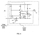
- Figure 4 shows another example of a current and voltage sense circuit with reduced current sense voltage threshold and improved current sense voltage threshold accuracy for an embodiment in accordance with the teachings of the present invention.
- Figure 5 shows yet another example of a current and voltage sense circuit with reduced current sense voltage threshold using a circuit technique known as "delta Vbe" to further reduce the current sense threshold voltage and improve its accuracy for an embodiment in accordance with the teachings of the present invention.
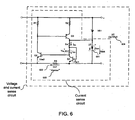
- Figure 6 shows yet another example of a current and voltage sense circuit with reduced current sense voltage threshold and improved thermal stability for an embodiment in accordance with the teachings of the present invention.
- Figure 7 shows yet another example of a current and voltage sense circuit with an accurate voltage reference for an embodiment in accordance with the teachings of the present invention.
- Figure 8 shows yet another example of a current and voltage sense circuit with example component values for an embodiment in accordance with the teachings of the present invention.
- Embodiments of a power supply regulator that may be utilized in a power supply are disclosed.
- numerous specific details are set forth in order to provide a thorough understanding of the present invention. It will be apparent, however, to one having ordinary skill in the art that the specific detail need not be employed to practice the present invention. Well-known methods related to the implementation have not been described in detail in order to avoid obscuring the present invention.
- An AC to DC CV/CC charger power supply circuit typically includes circuitry on the input or primary side which is electrically coupled to the AC input and circuitry on the secondary or output side of the power supply electrically coupled to a load such as a battery.
- Figure 1 shows an example of a low cost AC to DC CV/CC charger power supply.
- the power supply circuit example shown in Figure 1 is an isolated power supply as the input or primary side circuit side of the power supply is electrically isolated from the output or secondary side of the power supply. However, there are two couplings between input and output circuitry that are important to the operation of the power supply.
- the first is a magnetic coupling provided by the energy transfer element T1
- the second is an optical coupling provided by the photocoupler or optocoupler U2 where light output provided by current flowing in the light emitting diode (LED) 101 is detected by the phototransistor 102 providing a feedback signal which is coupled to the EN terminal of controller U1 on the primary or input side of the power supply.
- the example controller U1 shown in Figure 1 is TNY264, a member of the TinySwitch-II family of devices from Power Integrations, which integrates a switched mode power supply controller along with a high voltage MOSFET switch.
- the power supply output voltage and current regulation thresholds are determined by voltage and current sense circuitry on the secondary side of the power supply.
- the voltage regulation threshold is substantially equal to the breakdown voltage of zener diode VR3 and the base emitter junction voltage of bipolar transistor Q1.
- Resistors R7 and R4 also have secondary effects on the regulation voltage threshold.
- Resistor R7 reduces the gain of the voltage regulation circuit to help prevent instability.
- the voltage dropped across resistor R7 varies according to the current flowing in LED 101 and resistor R5 but, is negligible compared to the output voltage.
- the controller U1 requires a very low value of feedback current in the order of 250uA which results in a very small voltage drop across R7 of only approximately 1 mV since the current transfer ratio of the optocoupler U2 is approximately equal to 1.
- the output current regulation threshold of the power supply in Figure 1 is determined by the current sense circuit comprising R5 and the LED 101.
- the current sense circuit has no output until the voltage generated across current sense resistor R6 reaches a current sense threshold.
- the current sense threshold in the circuit of Figure 1 is substantially equal to the forward voltage drop of LED 101. When the voltage Vsense exceeds this current sense threshold, LED 101 provides light output which is the output of the current sense circuit.
- the exact current sense threshold is influenced slightly by the voltage dropped across resistor R5.
- the high power dissipated in the sense resistor also increases the power processed by the high voltage MOSFET in U2 and, in turn, increases losses in U2, further increasing the temperature of the enclosure. It is therefore, very desirable to have a low cost current sense circuit that provides a low current threshold to reduce overall power dissipation of an AC to DC CV/CC charger to increase its efficiency and to allow for smaller size enclosures.
- Figure 2 shows one embodiment of a circuit benefiting from the teachings of the present invention where the current sense threshold voltage has been substantially reduced.
- the voltage and current sense circuit shown in Figure 2 could be used in place of the voltage and current sense circuit of the power supply in Figure 1 .
- Output current Iout flows through current sense resistor R5 which converts the current to be sensed Iout into a current sense voltage Vsense which is applied to the input of a current sense circuit consisting of components Q1, Q2, R1, R2, R3, R4 and LED 201.
- the current sense threshold is the difference between the forward voltage drop of a first diode, which is the PN junction formed by the base emitter junction of Q1, having a value of Vbe1 and a fraction of the forward voltage of a second diode which is LED 201 forward voltage, V BIAS .
- This fraction of V BIAS is shown as voltage Vfr in Figure 2 created using a resistor divider formed by resistors R3 and R4.
- the forward voltage drop of the LED 201 which is relatively independent of current through the LED 201, acts as a voltage reference for the resistor divider circuit formed by R3 and R4 to generate fractional voltage Vfr.
- the benefit in the power supply circuit is clearly that the heat generated inside the power supply enclosure is reduced, in turn reducing thermal stress on the complete power supply and efficiency of the power supply is increased.
- the first bipolar transistor Q1 in Figure 2 is coupled to drive the base of second bipolar transistor Q2 as shown.
- Resistor R1 sets the current required to flow in Q 1 before the base emitter junction of Q2 conducts, which occurs when the current sense voltage reaches the current sense threshold. Once this current sense threshold is reached, Q2 turns on. The current flowing in Q2 then drives the LED 201, the light output of which forms the output of the current sense circuit.
- LED 201 is part of an optocoupler U1 where this light output is a feedback signal as for example in Figure 1 where LED 101 is a part of optocoupler U2 in a power supply circuit.
- LED 201 is a discrete LED where the light output is a visual indicator of the output current I202 reaching the current sense threshold.
- Resistor R2 at the emitter of Q2 in the circuit of Figure 2 is included to improve the current sense circuit performance when used in a CV/CC charger power supplies.
- control of the output current Iout 202 is often required even at very low values of the DC output voltage.
- Figure 3 highlights various operating regions in the output characteristics of a CV/CC charger power supply. At low output currents, the power supply operates in Region 1 where the output voltage is regulated at a voltage regulation threshold. In Figure 2 for example, this voltage regulation threshold voltage value would be determined by the breakdown voltage of VR1 added to the forward voltage drop of LED 201.
- Resistor R2 in Figure 2 introduces enough emitter impedance to allow first bipolar transistor Q1 collector to turn off the LED by pulling down the base of second transistor Q2 enough to clamp the collector voltage of Q2 through the PN junction diode of Q2 between collector and base, to a voltage that is less than the forward drop of the LED. In doing so, the current Ifdbk and therefore current sense circuit output, is rapidly reduced to substantially zero.
- the loss of output from the current sense circuit is a loss of the feedback signal and initiates auto-restart operation where the power switch internal to U1 stops switching for a long period and is restarted periodically for short periods of time to check whether a feedback signal can be received.
- Region 4 This auto-restart operation is represented in Figure 3 as Region 4.
- Region 4 could be a region in which the controller simply reduces the operating frequency or current limit of the power switch in order to force the power supply output current to reduce in this region. Regardless of the mode of operation in Region 4, the effect on the average output current is that it reduces.
- first bipolar transistor collector Q1 is no longer capable of clamping the collector of second bipolar transistor Q2 below the LED forward voltage, since there is now a very low impedance path from the DC output through the emitter base PN junction diode of second bipolar transistor Q2.
- the power supply output current will increase much more significantly as shown in Region 3 when the output voltage drops below approximately 1.2 V, before reaching the auto-restart Region 5 as shown in Figure 3 .
- This is undesirable in many applications, in which case it is necessary to include resistor R2 in series with the emitter of second bipolar transistor Q2.
- the use of R2 as shown eliminates the need for an additional secondary supply voltage and in many cases an associated secondary winding, to power the current sense circuit and maintain LED drive independent of output voltage, in order to prevent high output currents at low output voltages. Therefore, one of the advantages of the teachings of the present invention is that the current sense circuit operates directly off of the output voltage and offers low current sense threshold voltages without requiring an additional secondary supply voltage and or the associated additional secondary winding for proper operation at low output voltages.
- FIG 4 is another embodiment of a circuit benefiting from the teachings of the present invention with improved current sense circuit accuracy.
- the current sense threshold is again a voltage difference between a forward voltage drop of a first diode, being the base emitter PN junction of Q 1 and a fraction of the forward voltage drop of a second PN junction diode, which in Figure 4 is the base emitter PN junction of a diode connected bipolar transistor Q3, Vbe3.
- This base emitter voltage Vbe3 is applied across the resistor divider formed by R3 and R4, where the fraction of Vbe3 is equal to Vfr which is determined by the choice of values of R3 and R4.
- the second PN junction diode in Figure 4 is biased from the forward voltage drop of the LED 401 by the use of resistor R6.
- the circuit of Figure 4 has the advantage that by using bipolar transistors Q1 and Q3 of the same bipolar transistor part number, the part to part variation of the absolute value base emitter voltages between Q 1 and Q3 is relatively small reducing the variation in absolute value of current sense thresholds from one current sense circuit to another.
- the temperature coefficients of Vbe1 and Vbe3 will be substantially the same, which is approximately -3000 ppm/°C, which in absolute value is about -2.2mV/°C.
- thermal compensation is non ideal since the temperature coefficient of Vbe3 is itself divided down in value by the ratio of R3 and R4 and the temperature variation of Vfr will therefore be less than the temperature variation of Vbe1.
- the current sense threshold has a predictable temperature negative coefficient of approximately -3000 ppm/°C, similar to that of a Vbe independent of the absolute value of the current limit threshold. This temperature variation of the current sense threshold may be desirable in some applications. However, in most applications a zero temperature coefficient is preferred.
- the temperature variation of the current sense threshold of circuit in Figure 4 can be partially or fully offset by using higher emitter current density in Q1 compared to Q3 as will be explained later.
- V BLAS is well regulated independent of the value of the DC output voltage 404 over the entire Region 2 of CC operation shown in Figure 3 .
- This fact ensures that the PN junction diode voltage Vbe3 is relatively stable since emitter current density, which is set by R6 is substantially constant over a wide range of DC output voltage corresponding to region 2 of Figure 3 .
- the voltage across R6 is substantially temperature independent because, the Vbias, which is the forward voltage of the LED and the Vbe3 of the PN junction diode have very similar temperature coefficients.
- the very stable nature of the bias voltage V BIAS with respect to output voltage and temperature enables a further embodiment of a circuit benefiting from the teachings of the present invention as described below.
- Figure 5 shows yet another embodiment of a circuit benefiting from the teachings of the present invention using a circuit technique known as "delta Vbe” to further reduce the current sense threshold voltage and improve its accuracy.
- the principle of “delta Vbe” circuit techniques will be well known to one skilled in the art and has been used for many years in bandgap reference circuits for example.
- the technique relies on the fact that the difference in base emitter voltage drop of two bipolar transistors can be accurately predicted from the difference in their emitter current densities.
- two bipolar transistors exhibit a difference in their base emitter voltages of 60mV for every order of magnitude difference in their emitter current density levels.
- the absolute base emitter voltage threshold of bipolar transistors with the same emitter current density can vary by approximately 20mV.
- This error can be minimized by using a matched pair of transistors available from transistor manufacturers or by implementing these devices in an integrated circuit as matched transistors.
- this error can be corrected in production of the current sense circuit by trimming the value of R6 in order to ensure Vbe3 and Vbe1 maintain a difference of 60mV.
- the circuit in Figure 5 has a positive temperature coefficient on the current sense threshold of approximately 3000ppm/°C which may be desirable in some applications.
- a zero temperature coefficient of the current limit threshold is desired. This can be achieved in the circuit of Figure 4 by using the delta Vbe technique to partially or fully offset the positive temperature coefficient of the current sense threshold.
- the -3000 ppm/°C negative temperature coefficient of the current sense threshold can be substantially cancelled by using a lower emitter current density on Q3 relative to Q1 to create a voltage difference or delta Vbe between Vbe1 and Vbe3 that has a positive temperature coefficient. For example, if the threshold is set to 60 mV with Vbe1 same as Vbe2 , the temperature coefficient will be approximately -3000 ppm/°C.
- Vbe1 will increase by of 60 mV, and this delta Vbe will add to current sense threshold voltage but with a temperature coefficient of approximately +3000 ppm/°C resulting in a 120 mV threshold with near zero temperature coefficient.
- Figure 6 shows yet another embodiment of a circuit benefiting from the teachings of the present invention.
- the circuit of Figure 6 shows a current sense circuit where the current Iout 602 to be sensed or regulated is converted into a voltage Vsense 603.
- the current sense threshold of the circuit of Figure 6 is the sum of the Vbe2 of Q2 plus the voltage across R3 minus the Vbe1 of Q1.
- the current sense threshold is therefore substantially equal to the voltage across R3 as Vbe1 of Q1 will cancel the Vbe2 of Q2 to the first order.
- the current sense threshold is therefore equal to the voltage drop across resistor R3. Since one end of R3 is coupled directly to the base of Q1 and therefore at a base emitter PN junction voltage above the emitter voltage of Q1 and the other end of R3 is coupled to the collector of Q1, the voltage across R3 must be less than Vbe1.
- the practical range of voltage across R3 and therefore current sense threshold is between zero and (Vbe1- Vcesat1) where Vcesat1 is the minimum collector to emitter voltage of Q1 with a specified collector and base current. Vcesat1 is typically 0.2V and therefore, the voltage across R3 can be no more than approximately 0.5V.
- the base emitter voltage Vbe1 is 0.7V and V BIAS is 1 volt
- Typical values for R4 and R3 are 1000 ohms each.
- the benefit of the configuration in Figure 6 is that both the base emitter voltage drops Vbe1 and Vbe2 and therefore their temperature coefficients essentially cancel in equation (1), resulting in a current sense threshold that is substantially a function of the difference between the forward drop of the LED 601 and the forward drop of a PN junction, which is the Vbe1 of Q1. Since PN junction and LED forward voltages have very similar temperature coefficients, which are typically - 2.2mV/°C, the voltage across R3 (V R3 ), which substantially same as the current sense threshold of the circuit in Figure 6 is relatively temperature independent.
- the absolute base emitter voltages between Q 1 and Q2 can different by up to 20 mV in a high volume production environment due to part to part variations.
- this difference will have less influence in this circuit than in the circuit of Figure 5 since the current sense circuit of Figure 6 will typically use a current sense threshold voltage of 300mV and the 20mV difference in absolute base emitter voltage between Q1 and Q2 will therefore only introduce a small error.
- the part to part variations in forward voltage of LED and the Vbe1 of the bipolar transistor Q1 can cause even bigger differences in a production environment as those devices are manufactured in different technologies.
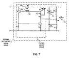
- FIG. 7 shows yet another embodiment of a circuit benefiting from the teachings of the present invention.
- This circuit uses an accurate voltage reference U3 to sense the voltage at the DC output 704 as opposed to low cost zener reference VR1 of Figure 6 .
- An example of U3 is TL431 voltage reference available from many semiconductor companies such as Texas Intruments, National Semiconductor, etc.
- TL431 voltage reference available from many semiconductor companies such as Texas Intruments, National Semiconductor, etc.
- one or more additional compensation components including for example capacitors and resistors, may be coupled between the terminals of U3 to provide control loop compensation in a practical circuit configuration. However these components are not shown here so as not to obscure the teachings of the present invention.
- the significance of the circuit shown in Fig 7 is that, other than the use of precision reference U3, the electrical performance is equivalent to the circuit of Figure 6 . Since U3 must be referenced to the negative rail of the DC output, it is therefore necessary to use current sense resistor R5 in the positive DC output rail and compared to the circuit of Figure 6 , invert the circuitry of the current sense circuit consisting of components R1, R2, R3, R4, Q1, Q2, Q3 and U3 LED 701 and use PNP bipolar transistors for Q1 and Q2 instead of NPNs used in Figure 6 .
- the sense circuit in Figure 7 is an electrical complement of the sense circuit in Figure 6 and therefore is electrically equivalent with same performance advantages. As would be obvious to one skilled in the art, all of the sense circuits that have discussed previously have compliment circuits that are electrically equivalent and therefore, part of the teachings of this invention.
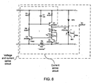
- FIG 8 shows one embodiment of a circuit benefiting from the teachings of the present invention with example component values included. This is a practical implementation of the current sense circuit of Figure 6 discussed above. Compared to the circuit in Figure 6 , two additional components are added which can be necessary in some applications of the invention in a power supply to prevent undesirable operating behavior. Capacitor C 1 and resistor R6 in Figure 8 , both help to avoid the power supply entering the Region 4 in Figure 2 when this is not desired under transient load conditions. For example, if C1 and R6 are not included and a sudden transient increase in output current demand is applied to the power supply DC output, the current flowing through current sense resistor R5 can transiently exceed the current sense regulation threshold before the power supply control loop has a chance to respond.
- Vsense can cause transistor Q1 to saturate and clamp the voltage across LED 801 as described above with reference to Figure 2 .
- This condition will force the power supply to operate in Region 4. This could be undesirable if the load transient is not intended to be large enough to drive the power supply to operate in this region.
- C 1 and R6 are therefore used to provide a time constant to control the time it takes for Q1 to clamp the voltage across LED 801 and therefore prevent this occurring under short transient load conditions.
- R6 could be replaced by a short circuit and C1 increased substantially to achieve a similar result.
Landscapes
- Engineering & Computer Science (AREA)
- Power Engineering (AREA)
- Physics & Mathematics (AREA)
- General Physics & Mathematics (AREA)
- Dc-Dc Converters (AREA)
- Control Of Voltage And Current In General (AREA)
Applications Claiming Priority (1)
| Application Number | Priority Date | Filing Date | Title |
|---|---|---|---|
| US11/121,808 US7310048B2 (en) | 2005-05-04 | 2005-05-04 | Method and apparatus for sensing a current in a circuit |
Publications (2)
| Publication Number | Publication Date |
|---|---|
| EP1720230A1 EP1720230A1 (en) | 2006-11-08 |
| EP1720230B1 true EP1720230B1 (en) | 2012-02-29 |
Family
ID=36693956
Family Applications (1)
| Application Number | Title | Priority Date | Filing Date |
|---|---|---|---|
| EP06252367A Not-in-force EP1720230B1 (en) | 2005-05-04 | 2006-05-04 | Power supply with current sensing circuit |
Country Status (3)
| Country | Link |
|---|---|
| US (2) | US7310048B2 (enExample) |
| EP (1) | EP1720230B1 (enExample) |
| JP (2) | JP2006313553A (enExample) |
Cited By (2)
| Publication number | Priority date | Publication date | Assignee | Title |
|---|---|---|---|---|
| DE102016202386B3 (de) * | 2016-02-17 | 2017-08-10 | Siemens Aktiengesellschaft | Spannungswandler mit einer Strommessvorrichtung |
| DE102017209833A1 (de) * | 2017-06-12 | 2018-12-13 | Robert Bosch Gmbh | Vorrichtung zur Umformung elektrischer Energie und Verfahren zur Bestimmung eines durch ein elektronisches Bauelement fließenden Stroms |
Families Citing this family (16)
| Publication number | Priority date | Publication date | Assignee | Title |
|---|---|---|---|---|
| US7255476B2 (en) * | 2004-04-14 | 2007-08-14 | International Business Machines Corporation | On chip temperature measuring and monitoring circuit and method |
| US7310048B2 (en) | 2005-05-04 | 2007-12-18 | Power Integrations, Inc. | Method and apparatus for sensing a current in a circuit |
| US7425834B2 (en) * | 2005-08-26 | 2008-09-16 | Power Integrations, Inc. | Method and apparatus to select a parameter/mode based on a time measurement |
| US7326947B2 (en) * | 2005-11-15 | 2008-02-05 | Avago Technologies Ecbu Ip Pte Ltd | Current transfer ratio temperature coefficient compensation method and apparatus |
| US8587269B2 (en) * | 2006-10-27 | 2013-11-19 | International Rectifier Corporation | Cycle by cycle synchronous buck converter control based on external clock |
| US8116106B2 (en) | 2008-09-19 | 2012-02-14 | Power Integrations, Inc. | Method and apparatus to select a parameter/mode based on a measurement during an initialization period |
| AU2010275527A1 (en) | 2009-07-24 | 2012-02-09 | Access Business Group International Llc | A wireless power supply |
| US20110113689A1 (en) * | 2009-11-16 | 2011-05-19 | Johnson Keith R | System And Method For Powering A Movable Barrier Operator |
| US8779777B2 (en) * | 2010-06-04 | 2014-07-15 | Linear Technology Corporation | Dynamic compensation of aging drift in current sense resistor |
| CN102788894A (zh) * | 2011-05-18 | 2012-11-21 | 鸿富锦精密工业(深圳)有限公司 | 电压侦测电路 |
| CN102612223A (zh) * | 2012-03-02 | 2012-07-25 | 苏州浩森电子科技有限公司 | 一种led驱动装置及其控制方法 |
| US9210758B2 (en) | 2012-10-16 | 2015-12-08 | General Electric Company | Boost converter of driver circuit with thermal compensation |
| JP5962593B2 (ja) * | 2013-06-07 | 2016-08-03 | 株式会社デンソー | 電流検出装置 |
| CN106877434A (zh) * | 2017-03-13 | 2017-06-20 | 四川力垦锂动力科技有限公司 | 一种蓄电池充电装置 |
| US10741348B2 (en) * | 2017-03-30 | 2020-08-11 | Richtek Technology Corporation | Power transmission apparatus |
| KR102646255B1 (ko) * | 2021-04-22 | 2024-03-11 | 엘에스일렉트릭(주) | 파워 디바이스 보호 장치 |
Family Cites Families (7)
| Publication number | Priority date | Publication date | Assignee | Title |
|---|---|---|---|---|
| US5198743A (en) * | 1990-12-11 | 1993-03-30 | Span, Inc. | Battery charger with microprocessor control |
| US5200692A (en) * | 1991-09-23 | 1993-04-06 | The Boeing Company | Apparatus for limiting current through a plurality of parallel transistors |
| US5698965A (en) * | 1995-12-01 | 1997-12-16 | Flight Systems, Inc. | Apparatus and method for determining the current state of charge of a battery by monitoring battery voltage increases above and decreases below a threshold |
| KR100285949B1 (ko) | 1996-12-12 | 2001-04-16 | 윤종용 | 배터리 충전회로 |
| US6795321B2 (en) * | 2001-07-20 | 2004-09-21 | Power Integrations, Inc. | Method and apparatus for sensing current and voltage in circuits with voltage across an LED |
| US6956487B2 (en) * | 2002-08-23 | 2005-10-18 | Motorola, Inc. | Battery charging status indication circuit |
| US7310048B2 (en) | 2005-05-04 | 2007-12-18 | Power Integrations, Inc. | Method and apparatus for sensing a current in a circuit |
-
2005
- 2005-05-04 US US11/121,808 patent/US7310048B2/en not_active Expired - Fee Related
-
2006
- 2006-05-04 EP EP06252367A patent/EP1720230B1/en not_active Not-in-force
- 2006-05-08 JP JP2006129010A patent/JP2006313553A/ja active Pending
-
2007
- 2007-11-13 US US11/939,356 patent/US7656304B2/en not_active Expired - Fee Related
-
2009
- 2009-04-20 JP JP2009102200A patent/JP2009165350A/ja active Pending
Cited By (2)
| Publication number | Priority date | Publication date | Assignee | Title |
|---|---|---|---|---|
| DE102016202386B3 (de) * | 2016-02-17 | 2017-08-10 | Siemens Aktiengesellschaft | Spannungswandler mit einer Strommessvorrichtung |
| DE102017209833A1 (de) * | 2017-06-12 | 2018-12-13 | Robert Bosch Gmbh | Vorrichtung zur Umformung elektrischer Energie und Verfahren zur Bestimmung eines durch ein elektronisches Bauelement fließenden Stroms |
Also Published As
| Publication number | Publication date |
|---|---|
| JP2006313553A (ja) | 2006-11-16 |
| JP2009165350A (ja) | 2009-07-23 |
| US20060250265A1 (en) | 2006-11-09 |
| US7310048B2 (en) | 2007-12-18 |
| US7656304B2 (en) | 2010-02-02 |
| EP1720230A1 (en) | 2006-11-08 |
| US20080068193A1 (en) | 2008-03-20 |
Similar Documents
| Publication | Publication Date | Title |
|---|---|---|
| US7656304B2 (en) | Method and apparatus for sensing a current in a circuit | |
| US6795321B2 (en) | Method and apparatus for sensing current and voltage in circuits with voltage across an LED | |
| US7894219B2 (en) | Method and apparatus of low current startup circuit for switching mode power supplies | |
| US7339359B2 (en) | Terminal for multiple functions in a power supply | |
| US7948780B2 (en) | Semiconductor device for switching power supply control, startup circuit, and startup method for switching power supply device | |
| US7315461B2 (en) | Power supply device | |
| CN104571241B (zh) | 电压稳压电路及其方法 | |
| KR101489962B1 (ko) | 전력 변환기, 그 스위칭 제어 장치 및 구동 방법 | |
| US20120087053A1 (en) | Constant voltage power supply circuit | |
| US20220045540A1 (en) | Systems and methods for adjusting input power and/or output power of charging systems | |
| US20220182049A1 (en) | Semiconductor integrated circuit device | |
| US7518836B2 (en) | Switching mode power supply and method for performing protection operation thereof | |
| KR20120046095A (ko) | 고효율의 열적으로 안정된 레귤레이터 및 조정 가능한 제너 다이오드 | |
| JP2006079612A (ja) | 帰還回路におけるパラメータ変動の補償 | |
| CN201022180Y (zh) | 一次侧反馈控制交换式电源供应器 | |
| EP1856784B1 (en) | Control apparatus and method of regulating power | |
| US20070091651A1 (en) | Switching mode power supply | |
| US12095252B2 (en) | Overcurrent protection circuit | |
| US8446180B2 (en) | Semiconductor device | |
| EP1750137A2 (en) | Method and apparatus for low cost current and voltage sensing in circuits as a function of a voltage drop | |
| Liu et al. | Design of wide power supply, high performance voltage regulator with BCD process | |
| RU2282233C1 (ru) | Импульсный стабилизатор | |
| US10530246B2 (en) | Charge pump circuit and method for operating a charge pump circuit | |
| JP2000010646A (ja) | 安定化電源回路 |
Legal Events
| Date | Code | Title | Description |
|---|---|---|---|
| PUAI | Public reference made under article 153(3) epc to a published international application that has entered the european phase |
Free format text: ORIGINAL CODE: 0009012 |
|
| AK | Designated contracting states |
Kind code of ref document: A1 Designated state(s): AT BE BG CH CY CZ DE DK EE ES FI FR GB GR HU IE IS IT LI LT LU LV MC NL PL PT RO SE SI SK TR |
|
| AX | Request for extension of the european patent |
Extension state: AL BA HR MK YU |
|
| 17P | Request for examination filed |
Effective date: 20070105 |
|
| 17Q | First examination report despatched |
Effective date: 20070208 |
|
| AKX | Designation fees paid |
Designated state(s): DE FR GB IT NL SE |
|
| RAP3 | Party data changed (applicant data changed or rights of an application transferred) |
Owner name: POWER INTEGRATIONS, INC. |
|
| GRAP | Despatch of communication of intention to grant a patent |
Free format text: ORIGINAL CODE: EPIDOSNIGR1 |
|
| GRAS | Grant fee paid |
Free format text: ORIGINAL CODE: EPIDOSNIGR3 |
|
| GRAA | (expected) grant |
Free format text: ORIGINAL CODE: 0009210 |
|
| AK | Designated contracting states |
Kind code of ref document: B1 Designated state(s): DE FR GB IT NL SE |
|
| REG | Reference to a national code |
Ref country code: GB Ref legal event code: FG4D |
|
| REG | Reference to a national code |
Ref country code: DE Ref legal event code: R096 Ref document number: 602006027895 Country of ref document: DE Effective date: 20120426 |
|
| REG | Reference to a national code |
Ref country code: NL Ref legal event code: VDEP Effective date: 20120229 |
|
| PG25 | Lapsed in a contracting state [announced via postgrant information from national office to epo] |
Ref country code: NL Free format text: LAPSE BECAUSE OF FAILURE TO SUBMIT A TRANSLATION OF THE DESCRIPTION OR TO PAY THE FEE WITHIN THE PRESCRIBED TIME-LIMIT Effective date: 20120229 |
|
| PG25 | Lapsed in a contracting state [announced via postgrant information from national office to epo] |
Ref country code: SE Free format text: LAPSE BECAUSE OF FAILURE TO SUBMIT A TRANSLATION OF THE DESCRIPTION OR TO PAY THE FEE WITHIN THE PRESCRIBED TIME-LIMIT Effective date: 20120229 |
|
| PG25 | Lapsed in a contracting state [announced via postgrant information from national office to epo] |
Ref country code: IT Free format text: LAPSE BECAUSE OF FAILURE TO SUBMIT A TRANSLATION OF THE DESCRIPTION OR TO PAY THE FEE WITHIN THE PRESCRIBED TIME-LIMIT Effective date: 20120229 |
|
| PLBE | No opposition filed within time limit |
Free format text: ORIGINAL CODE: 0009261 |
|
| STAA | Information on the status of an ep patent application or granted ep patent |
Free format text: STATUS: NO OPPOSITION FILED WITHIN TIME LIMIT |
|
| GBPC | Gb: european patent ceased through non-payment of renewal fee |
Effective date: 20120529 |
|
| 26N | No opposition filed |
Effective date: 20121130 |
|
| REG | Reference to a national code |
Ref country code: FR Ref legal event code: ST Effective date: 20130131 |
|
| REG | Reference to a national code |
Ref country code: DE Ref legal event code: R097 Ref document number: 602006027895 Country of ref document: DE Effective date: 20121130 |
|
| PG25 | Lapsed in a contracting state [announced via postgrant information from national office to epo] |
Ref country code: GB Free format text: LAPSE BECAUSE OF NON-PAYMENT OF DUE FEES Effective date: 20120529 Ref country code: FR Free format text: LAPSE BECAUSE OF NON-PAYMENT OF DUE FEES Effective date: 20120531 |
|
| PGFP | Annual fee paid to national office [announced via postgrant information from national office to epo] |
Ref country code: DE Payment date: 20140529 Year of fee payment: 9 |
|
| REG | Reference to a national code |
Ref country code: DE Ref legal event code: R119 Ref document number: 602006027895 Country of ref document: DE |
|
| PG25 | Lapsed in a contracting state [announced via postgrant information from national office to epo] |
Ref country code: DE Free format text: LAPSE BECAUSE OF NON-PAYMENT OF DUE FEES Effective date: 20151201 |