EP1719210B1 - Connector apparatus - Google Patents
Connector apparatus Download PDFInfo
- Publication number
- EP1719210B1 EP1719210B1 EP05711713A EP05711713A EP1719210B1 EP 1719210 B1 EP1719210 B1 EP 1719210B1 EP 05711713 A EP05711713 A EP 05711713A EP 05711713 A EP05711713 A EP 05711713A EP 1719210 B1 EP1719210 B1 EP 1719210B1
- Authority
- EP
- European Patent Office
- Prior art keywords
- header
- connector
- openings
- shield
- shield blades
- Prior art date
- Legal status (The legal status is an assumption and is not a legal conclusion. Google has not performed a legal analysis and makes no representation as to the accuracy of the status listed.)
- Expired - Lifetime
Links
- 238000003780 insertion Methods 0.000 claims description 27
- 230000037431 insertion Effects 0.000 claims description 24
- 239000000463 material Substances 0.000 claims description 9
- 238000000034 method Methods 0.000 claims description 3
- 241001136800 Anas acuta Species 0.000 description 6
- 230000013011 mating Effects 0.000 description 4
- 229920000106 Liquid crystal polymer Polymers 0.000 description 2
- 239000004977 Liquid-crystal polymers (LCPs) Substances 0.000 description 2
- 239000004020 conductor Substances 0.000 description 2
- 230000007423 decrease Effects 0.000 description 2
- 230000003247 decreasing effect Effects 0.000 description 2
- 239000011810 insulating material Substances 0.000 description 2
- 239000011159 matrix material Substances 0.000 description 2
- 229910000881 Cu alloy Inorganic materials 0.000 description 1
- 239000000956 alloy Substances 0.000 description 1
- 230000005540 biological transmission Effects 0.000 description 1
- 230000015556 catabolic process Effects 0.000 description 1
- 238000006731 degradation reaction Methods 0.000 description 1
- 239000012777 electrically insulating material Substances 0.000 description 1
- 238000004806 packaging method and process Methods 0.000 description 1
- 239000004033 plastic Substances 0.000 description 1
- 239000012815 thermoplastic material Substances 0.000 description 1
Images

Classifications
-
- H—ELECTRICITY
- H01—ELECTRIC ELEMENTS
- H01R—ELECTRICALLY-CONDUCTIVE CONNECTIONS; STRUCTURAL ASSOCIATIONS OF A PLURALITY OF MUTUALLY-INSULATED ELECTRICAL CONNECTING ELEMENTS; COUPLING DEVICES; CURRENT COLLECTORS
- H01R13/00—Details of coupling devices of the kinds covered by groups H01R12/70 or H01R24/00 - H01R33/00
- H01R13/648—Protective earth or shield arrangements on coupling devices, e.g. anti-static shielding
- H01R13/658—High frequency shielding arrangements, e.g. against EMI [Electro-Magnetic Interference] or EMP [Electro-Magnetic Pulse]
- H01R13/6581—Shield structure
- H01R13/6585—Shielding material individually surrounding or interposed between mutually spaced contacts
-
- H—ELECTRICITY
- H01—ELECTRIC ELEMENTS
- H01R—ELECTRICALLY-CONDUCTIVE CONNECTIONS; STRUCTURAL ASSOCIATIONS OF A PLURALITY OF MUTUALLY-INSULATED ELECTRICAL CONNECTING ELEMENTS; COUPLING DEVICES; CURRENT COLLECTORS
- H01R12/00—Structural associations of a plurality of mutually-insulated electrical connecting elements, specially adapted for printed circuits, e.g. printed circuit boards [PCB], flat or ribbon cables, or like generally planar structures, e.g. terminal strips, terminal blocks; Coupling devices specially adapted for printed circuits, flat or ribbon cables, or like generally planar structures; Terminals specially adapted for contact with, or insertion into, printed circuits, flat or ribbon cables, or like generally planar structures
- H01R12/70—Coupling devices
- H01R12/71—Coupling devices for rigid printing circuits or like structures
-
- H—ELECTRICITY
- H01—ELECTRIC ELEMENTS
- H01R—ELECTRICALLY-CONDUCTIVE CONNECTIONS; STRUCTURAL ASSOCIATIONS OF A PLURALITY OF MUTUALLY-INSULATED ELECTRICAL CONNECTING ELEMENTS; COUPLING DEVICES; CURRENT COLLECTORS
- H01R12/00—Structural associations of a plurality of mutually-insulated electrical connecting elements, specially adapted for printed circuits, e.g. printed circuit boards [PCB], flat or ribbon cables, or like generally planar structures, e.g. terminal strips, terminal blocks; Coupling devices specially adapted for printed circuits, flat or ribbon cables, or like generally planar structures; Terminals specially adapted for contact with, or insertion into, printed circuits, flat or ribbon cables, or like generally planar structures
- H01R12/50—Fixed connections
- H01R12/51—Fixed connections for rigid printed circuits or like structures
- H01R12/55—Fixed connections for rigid printed circuits or like structures characterised by the terminals
- H01R12/58—Fixed connections for rigid printed circuits or like structures characterised by the terminals terminals for insertion into holes
-
- Y—GENERAL TAGGING OF NEW TECHNOLOGICAL DEVELOPMENTS; GENERAL TAGGING OF CROSS-SECTIONAL TECHNOLOGIES SPANNING OVER SEVERAL SECTIONS OF THE IPC; TECHNICAL SUBJECTS COVERED BY FORMER USPC CROSS-REFERENCE ART COLLECTIONS [XRACs] AND DIGESTS
- Y10—TECHNICAL SUBJECTS COVERED BY FORMER USPC
- Y10T—TECHNICAL SUBJECTS COVERED BY FORMER US CLASSIFICATION
- Y10T29/00—Metal working
- Y10T29/53—Means to assemble or disassemble
- Y10T29/5313—Means to assemble electrical device
- Y10T29/532—Conductor
- Y10T29/53209—Terminal or connector
Definitions
- This invention relates to electrical connectors, and particularly to high-speed electrical connectors for attachment to printed circuit boards.
- Coaxial and shielded cables are available to carry signals from a transmission point to a reception point, and reduce the likelihood that the signal carried in one shielded or coaxial cable will interfere with the signal carried by another shielded or coaxial cable in close proximity.
- the shielding is often lost, thereby allowing interference and crosstalk between signals.
- the use of individual shielded wires and cables is not desirable at points of connections due to the need for making a large number of connections in a very small space.
- the known connector comprises a body of electrically insulating material having contact holes each provided with an electrical conductive contact element and arranged in at least two columns and at least two rows.
- shielding elements of electrically conductive plate material are disposed in the body. The shielding elements are wave-shaped and arranged so that neighboring contact elements are always entirely shielded from each other.
- EP-A-0 374 307 discloses a connector for printed circuit boards comprising first and second connector elements.
- the first connector element has a first housing of insulating material including a base and two spaced upright sidewalls extending parallel to each other from the base and defining a contact region. Further the first connector element is provided with a plurality of rows of male contacts which are press-fit in the printed circuit boards and extend through the base into the contact region of the first housing.
- the second connector element has a second housing of insulating material including outwardly directed sidewalls adapted to be fitted between the sidewalls of the first housing.
- the second connector element is further provided with a plurality of rows of female contacts having contact portions for contacting the male contacts of the first housing when the second housing is received between the sidewalls of the first housing. Shield elements are not provided in this connector.
- the header connector includes a header body having an internal surface and an external surface.
- the header body includes a plurality of first openings and a plurality of second openings extending from the internal surface to the external surface.
- a plurality of signal pins are configured for insertion into the plurality of first openings to form an array of pin contacts extending from the internal surface of the header body.
- a plurality of shield blades are configured for insertion into the plurality of second openings.
- Each of the plurality of shield blades has at a first end thereof a generally right angle shielding portion configured to be disposed adjacent to a corresponding one of the plurality of signal pins. The first ends of the plurality of shield blades are substantially coplanar with the internal surface of the header body.
- the connector system includes a first header body and a second header body.
- the first and second header bodies have a front wall formed to include a plurality of first openings and a plurality of second openings therethrough.
- the first and second header bodies are positioned on opposite sides of a printed circuit board.
- a plurality of signal pins are configured for insertion in the plurality of first openings in the first and second header bodies. Each of the plurality of signal pins extends continuously through the first openings of the first and second header bodies and the printed circuit board.
- a first plurality of shield blades is configured for insertion in the plurality of second openings in the first header body, and a second plurality of shield blades configured for insertion in the plurality of second openings in the second header body.
- Each shield blade of the first plurality of shield blades has a first end that is substantially coplanar with an internal surface of the first front wall.
- the connector system includes a header connector and a socket connector configured to mate with the header connector.
- the header connector has a front wall with an internal surface.
- the front wall includes a plurality of first openings and a plurality of second openings extending therethrough.
- a plurality of signal pins are inserted in the plurality of first openings to form an array of pin contacts extending above the internal surface of the header body.
- a plurality of shield blades are inserted in the plurality of second openings. Each of the plurality of shield blades has a first end that is substantially coplanar with the internal surface of the header body.
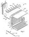
- FIGS 1 , 2, and 3 show a header connector 100 in accordance with the present invention.
- the header connector 100 is configured for attachment to a printed circuit board 30 and connection to a mating socket connector 200 (shown in Figure 5 ).
- the header connector 100 includes a header body 102, a plurality of signal pins 104, a continuous strip of material having a plurality of shield blades 106 formed therein, and a plurality of ground pins 108. Except for their length, the ground pins 108 are substantially identical to the signal pins 104.
- the header body 102 is formed to include a vertical front wall 110, and top and bottom laterally-extending, horizontal walls 112 and 114 projecting perpendicularly therefrom.
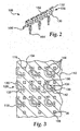
- the front wall 110 is formed to include a plurality of first signal-pin-receiving openings 116, a plurality of second shield-blade-receiving openings 118, and a plurality of third ground-pin-receiving openings 120, all of which extend between an internal surface 122 and an external surface 124 of front wall 110.
- the plurality of second shield-blade-receiving openings 118 are formed to have a generally right angle cross-section.
- the openings 116, 118, 120 may include chamfered entrances at one or both of internal surface 122 and external surface 124 to assist in the insertion of pins 104, 108 and shield blades 106.
- the plurality of signal pins 104 are configured for insertion into the plurality of first signal-pin-receiving openings 116 in the header connector 100 to form an array of signal pins 104 which are configured for reception in an array of pin-insertion windows 230 in mating socket connector 200 (shown in Figure 5 ), when the socket connector 200 is inserted into the header connector 100.
- Each signal pin 104 includes a first end 152 extending above the front wall 110 of the header connector 100, and a second end 154 spaced apart from the first end 152 and configured for insertion into an opening 32 in printed circuit board 30.
- the plurality of shield blades 106 are formed to include a generally right angle shielding portion 128 configured to be inserted into the plurality of second, generally right angle shield-blade-receiving openings 118.
- the generally right angle shielding portion 128 of each of the plurality of shield blades 106 includes substantially perpendicular first leg portion 130 and second leg portion 132.
- Each shield blade 106 includes a first end 162 and a second end 164.
- the generally right angle shielding portion 128 preferably extends to first end 162.
- first end 162 of shield blade 106 When inserted into header body 102, the first end 162 of shield blade 106 extends to the plane of internal surface 122 of the front wall 110 of the header connector 100, adjacent to a signal pin 104, such that first end 162 is substantially coplanar with internal surface 122. First end 162 may be positioned slightly above or below the plane of internal surface 122.
- the second end 164 of each shield blade 106 is spaced apart from the first end 162 and configured for insertion into a hole 34 in the printed circuit board 30 adjacent to the second end 154 of the signal pin 104.
- second ends 164 of shield blades 106 are electrically connected to a ground plane 40 within printed circuit board 30.
- shield blades 106 are commonly grounded.
- shield blades are not commonly grounded.
- at least one signal pin 104 is electrically connected with ground plane 40 and commonly grounded with at least shield blade 106 via the ground plane.
- first signal-pin-receiving openings 116 and the second shield-blade-receiving openings 118 are arranged symmetrically in the front wall 110 of the header body 102 such that the generally right angle shielding portions 128 of shield blades 106 substantially surround the signal pins 104 to form a coaxial shield around each of the plurality of signal pins 104.
- Each of the plurality of second, generally right angle shield-blade-receiving openings 118 includes a central portion 134 coupled to first and second end portions 136 and 138 by first and second narrowed throat portions 140 and 142.
- the first and second narrowed throat portions 140 and 142 are dimensioned to frictionally engage the first and second leg portions 130 and 132 of the shield blades 106 to hold the shield blades 106 in place.
- the central portion 134 and the first and second end portions 136 and 138 of each of the plurality of second generally right angle openings 118 are formed to provide air gaps 144 surrounding the generally right angle shield portion 128 of a shield blade 106.
- the geometry and dimensions of the air gaps 144, the geometry, dimensions and material of the right angle shielding portions 128, and the geometry, dimensions and material of the header body 102 surrounding the air gaps 144 are configured to tune the header connector 100 to match a specified impedance (for example, 50 ohms).
- the configuration of the right angle shield blades 106 lends itself to mass production in a continuous strip in a manner that economizes material usage.
- a plurality of ground pins 108 are configured for insertion into the plurality of third ground-pin-receiving openings 120 in the front wall 110 of the header connector 100.
- the plurality of ground pins 108 are configured to engage contact arms 296 of corresponding grounding structures of socket connector 200 when the socket connector 200 is inserted into the header connector 100 as shown in Figure 5 .
- Each ground pin 108 includes a first end 172 extending above the front wall 110 of the header connector 100, and a second end 174 spaced apart from the first end 172 and configured for insertion into a hole 38 in printed circuit board 30, where electrical contact with ground plane 30 is provided. If socket connector 200 does not include or require a grounding contact, ground pins 108 may be omitted from header 100.
- Each of the plurality of signal pins 104 and ground pins 108 includes a pin tail 146, and each strip of shield blades 106 includes at least one shield tail 148.
- the number of shield tails 148 may be the same as the number of shield blades 106, or may be different than the number of shield blades 106.
- each strip of shield blades 106 has a plurality of shield tails 148, with one shield tail 148 for every two shield blades 106, wherein the shield tails 148 are staggered and aligned with alternate shield blades 106 along the strip of shield blades 106.
- shield tails 148 may be provided, with the shield tails 148 either uniformly or non-uniformly spaced along the length of the strip of shield blades 106.
- Embodiments having staggered shield tails 148 on shield blades 106 are particularly useful in back-to-back mounting of header connectors 100 on a printed circuit board, as described with respect to Figure 7 , as the staggered shield tails 148 permit back-to-back mounting of header connectors 100 without interference between shield tails 148 of the opposing header connectors 100.
- pin tails 146 and shield tails 148 are positioned in an evenly spaced matrix, such that back-to-back mounted header connectors may be mounted orthogonally to each other.
- the pin tails 146 and the shield tails 148 extend outwardly from the external surface 124 of the front wall 110.
- the pin tails 146 and shield tails 148 of header 100 can be either press fitted into the holes 32, 34 in the printed circuit board 30 or soldered thereto. Alternatively, the pin tails 146 and shield tails 148 could instead be surface mounted to the printed circuit board 30.
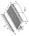
- Figure 4 is a perspective view showing first and second header bodies 102, 102' positioned end to end, and one of a plurality of continuous strips of shield blades 106 configured for insertion into a row of shield-blade-receiving openings 118 in the first and second header bodies 102, 102'.
- the continuous strips of shield blades 106 extend between the first and second header bodies 102, 102' to tie them together to form a monoblock.
- the continuous strips of shield blades 106 can be used to connect any number of header connectors 100 to create header connectors of variable length.
- the strip of shield blades 106 may be formed to include a right angle tab 106' at opposite ends thereof to provide a secure connection between the header bodies 102.
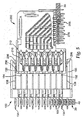
- socket connector 200 is illustrated in Figure 5 , as socket connector 200 is mated with header 100.
- Socket connector 200 may be any of a variety of connector types, such as a connector configured for connection to a printed circuit board or a cable connector.
- socket connector 200 is a hard metric connector according to industry standard IEC 61076-4-101.
- socket connector 200 is a hard metric connector according to the COMPACTPCI or FUTUREBUS industry standards.
- socket connector 200 includes a plurality of signal contacts 210 for making electrical contact with the array of signal pins 104 of the header connector 100, and at least one shielding element 212 associated with the plurality of signal contacts 210.
- the at least one shielding element 212 of the socket connector 200 comprises a plurality of strip line shielding elements associated with the plurality of signal contacts 210.
- socket connector 200 may be provided with signal tails 206 and shield tails 276 that can be either press fitted into the holes in the printed circuit boards or soldered thereto.
- the pin tails 206 and shield tails 276 could instead be surface mounted to the printed circuit boards.
- Figure 5 shows assembly of the header connector 100 with socket connector 200.
- External guide means such as guide slots 150 or guide pins (not shown) may be provided on the opposite sides of the header connector 100 to guide the insertion of the socket connector 200 into the header connector 100 so that the array of pin-insertion windows 230 in the socket connector 200 are aligned with the array of signal pins 104 in the header connector 100 prior to insertion of the signal pins 104 into mating receptacle contacts 204 of the socket connector 200.
- signal pins 104 of header 100 make electrical contact with signal contacts 210 of socket connector 200.
- the shield blades 106 of the header connector 100 are too short to contact any shielding elements 212 of the socket connector 200.
- the plurality of shield blades 106 of the header connector 100 and the at least one shielding element 212 of the socket connector 200 are unable to make electrical contact when the header connector 100 and the socket connector 200 are in a mated condition. In other embodiments, inadvertent or intermittent contact between shield blades 106 of the header connector 100 and the at least one shielding element 212 of the socket connector 200 is possible, although unnecessary. If provided, the ground pins 108 of the header connector 100 may contact corresponding contact arms 296 or similar structure of socket connector 200.
- shield blades 106 of header connector 100 do not make grounding electrical contact with shielding elements 212 of socket connector 200, one skilled in the art would not expect the provision of shield blades 106 to improve the electrical performance of the interconnect over a header lacking shield blades, and specifically would not expect a decrease in crosstalk.
- the crosstalk experienced in the interconnection decreases unexpectedly.
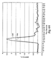
- the graph of Figure 6A illustrates a signal having a 35ps rise time
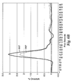
- the graph of Figure 6b illustrates a signal having a 100ps rise time.
- the crosstalk decreased from approximately 3.5% for a header lacking shield blades 106 (line 300) to approximately 2.5% for a header provided with shield blades 106 (line 302), providing an improvement of over 28%.
- the crosstalk decreased from approximately 3.1% for a header lacking shield blades 106 (line 300') to approximately 2.3% for a header provided with shield blades 106 (line 302'), providing an improvement of over 25%.
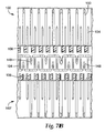
- First and second header connectors 100, 100' are positioned back-to-back on opposite sides of printed circuit board 30.
- the first and second header connectors 100, 100' are each generally constructed as described above, and each includes header body 102, signal pins 104, shield blades 106, and optional ground pins 108.
- shield blades 106 of one header connector 100, 100' may alternately extend above the plane of interior surface 122 for connection to a shielded socket connector, as illustrated by dashed lines 107.
- the mating socket connector 200 may have relief areas to receive the extended shield blades 107.
- the plurality of signal pins 104 and optional ground pins 108 are configured for insertion into the plurality of first signal-pin-receiving openings 116 in the header connectors 100, 100', as described above, except that pins 104, 108 extend continuously through first header connector 100, printed circuit board 30 and second header connector 100' to form an array of signal pins 104 on both sides of printed circuit board 30.
- the plurality of shield blades 106 of first and second header connectors 100, 100' are formed as described above, with generally right angle shielding portions 128 configured to be inserted into the plurality of second, generally right angle shield-blade-receiving openings 118.
- the shield tails 148 of each shield blade 106 are configured for insertion into the printed circuit board 30 and are staggered as described above, such that the shield tails of the opposing header connectors 100, 100'do not interfere with each other.
- shield tails 148 are positioned in a uniform matrix, such that the longitudinal axes of header connectors 100, 100' may be positioned orthogonal to each other, if desired for a particular application.
- shield tails 148 of shield blades 106 of first and second header connectors 100, 100' are electrically connected to ground plane 40 within printed circuit board 30.
- shield blades 106 are commonly grounded.
- shield blades are not commonly grounded.
- at least one signal pin 104 is electrically connected with ground plane 40 and commonly grounded with at least shield blade 106 via the ground plane 40.
- the header connector 100 described herein provides other advantages, particularly in assembly of the header connector 100 and attachment to a printed circuit board 30.
- shield blades 106 and pins 104, 108 may all be inserted into header body 102 prior to attachment to printed circuit board 30.
- shield blades 106 may be first inserted into header body 102, and the header sans pins 104, 108 may be aligned with and secured to printed circuit board 30, via shield tails 148. Openings 116, 120 in header body 102 may then be used as insertion guides and straighteners for pins 104, 108, thereby reducing the probability of stubbing or otherwise damaging pins 104, 108 during assembly.
- Chamfered entrances for openings 116, 120 may be provided at one or both of internal surface 122 and external surface 124 to assist in the insertion of pins 104, 108. These assembly methods may be combined when mounting header connectors back-to-back on a printed circuit board, as illustrated in Figure 7 . In that instance, a first header connector 100 without pins 104, 108 may be mounted on one side of the printed circuit board 30, and then a second header connector 100 with pins 104, 108 may be installed on the opposing side of the printed circuit board 30.
- Chamfered entrances for openings 116, 120 at external surface 124 is useful in this assembly method, for capturing pins 104, 108 as they come through circuit board 30.
- shield tails 148 provides additional resistance to pull-out forces is provided to header connector 100.
- header connector 100 and socket connector 200 are molded from suitable thermoplastic material, such as liquid crystal polymer ("LCP"), having the desired mechanical and electrical properties for the intended application.
- LCP liquid crystal polymer
- the conductive metallic parts are made from, for example, plated copper alloy material, although other suitable materials will be recognized by those skilled in the art.
- the connector materials, geometry and dimensions are all designed to maintain a specified impedance throughout the part.
Landscapes
- Details Of Connecting Devices For Male And Female Coupling (AREA)
- Coupling Device And Connection With Printed Circuit (AREA)
- Containers And Packaging Bodies Having A Special Means To Remove Contents (AREA)
- Paper (AREA)
- Measurement And Recording Of Electrical Phenomena And Electrical Characteristics Of The Living Body (AREA)
- Yarns And Mechanical Finishing Of Yarns Or Ropes (AREA)
Applications Claiming Priority (2)
| Application Number | Priority Date | Filing Date | Title |
|---|---|---|---|
| US10/788,684 US7513797B2 (en) | 2004-02-27 | 2004-02-27 | Connector apparatus |
| PCT/US2005/001823 WO2005093908A1 (en) | 2004-02-27 | 2005-01-19 | Connector apparatus |
Publications (2)
| Publication Number | Publication Date |
|---|---|
| EP1719210A1 EP1719210A1 (en) | 2006-11-08 |
| EP1719210B1 true EP1719210B1 (en) | 2010-03-03 |
Family
ID=34887050
Family Applications (1)
| Application Number | Title | Priority Date | Filing Date |
|---|---|---|---|
| EP05711713A Expired - Lifetime EP1719210B1 (en) | 2004-02-27 | 2005-01-19 | Connector apparatus |
Country Status (9)
| Country | Link |
|---|---|
| US (2) | US7513797B2 (enExample) |
| EP (1) | EP1719210B1 (enExample) |
| JP (1) | JP2007525808A (enExample) |
| KR (1) | KR101121836B1 (enExample) |
| CN (1) | CN1926723B (enExample) |
| AT (1) | ATE459994T1 (enExample) |
| DE (1) | DE602005019693D1 (enExample) |
| IL (1) | IL177646A0 (enExample) |
| WO (1) | WO2005093908A1 (enExample) |
Families Citing this family (22)
| Publication number | Priority date | Publication date | Assignee | Title |
|---|---|---|---|---|
| US20070141871A1 (en) * | 2005-12-19 | 2007-06-21 | 3M Innovative Properties Company | Boardmount header to cable connector assembly |
| US8550852B2 (en) * | 2007-05-23 | 2013-10-08 | Fci | Electrical connector with staggered single ended contacts |
| CN101459299B (zh) * | 2007-12-11 | 2010-11-17 | 富士康(昆山)电脑接插件有限公司 | 电连接器 |
| US8221162B2 (en) * | 2008-07-24 | 2012-07-17 | 3M Innovative Properties Company | Electrical connector |
| US7621760B1 (en) | 2008-07-24 | 2009-11-24 | 3M Innovative Properties Company | Electrical connector |
| TWM358444U (en) * | 2008-12-30 | 2009-06-01 | Advanced Connectek Inc | Electric connector suitable for transmitting a high-frequency signal |
| DE102009057260A1 (de) * | 2009-12-08 | 2011-08-04 | ERNI Electronics GmbH, 73099 | Relief-Steckverbinder und Multilayerplatine |
| CN102782955B (zh) * | 2009-12-30 | 2015-05-20 | Fci公司 | 具有电绝缘壳体以及共用接地触头的电连接器 |
| US9240638B2 (en) | 2011-03-17 | 2016-01-19 | Molex, Llc | Mezzanine connector with terminal brick |
| US8430691B2 (en) * | 2011-07-13 | 2013-04-30 | Tyco Electronics Corporation | Grounding structures for header and receptacle assemblies |
| US8840432B2 (en) * | 2012-04-24 | 2014-09-23 | Tyco Electronics Corporation | Circuit board and wire assembly |
| JP5863041B2 (ja) * | 2012-06-01 | 2016-02-16 | アルプス電気株式会社 | 電子部品用ソケット |
| US8777663B2 (en) * | 2012-11-26 | 2014-07-15 | Tyco Electronics Corporation | Receptacle assembly having a commoning clip with grounding beams |
| CN103280670A (zh) * | 2013-05-17 | 2013-09-04 | 连展科技电子(昆山)有限公司 | 抑制讯号干扰的插座电连接器 |
| US20160359278A1 (en) * | 2014-02-04 | 2016-12-08 | Molex, Llc | Connector with thermal ventilation |
| US9559465B2 (en) * | 2014-07-29 | 2017-01-31 | Tyco Electronics Corporation | High speed signal-isolating electrical connector assembly |
| CN105990763B (zh) * | 2015-02-15 | 2019-10-29 | 泰科电子(上海)有限公司 | 电连接器 |
| US10096924B2 (en) * | 2016-11-21 | 2018-10-09 | Te Connectivity Corporation | Header contact for header connector of a communication system |
| US10326244B2 (en) * | 2017-09-06 | 2019-06-18 | Te Connectivity Corporation | Electrical connector and electrical contact configured to reduce resonance |
| CN111129808B (zh) * | 2018-10-30 | 2021-07-30 | 上海航天科工电器研究院有限公司 | 接地端子组件、电连接器及电连接器组件 |
| CN113612082B (zh) * | 2021-02-09 | 2022-07-29 | 中航光电科技股份有限公司 | 一种导电扣板 |
| WO2025003782A1 (en) * | 2023-06-30 | 2025-01-02 | Molex, Llc | Resting pocket contact connector |
Family Cites Families (34)
| Publication number | Priority date | Publication date | Assignee | Title |
|---|---|---|---|---|
| US3936466A (en) | 1974-04-01 | 1976-02-03 | Interx Research Corporation | 3-Chloro-tetrahydro-1,3-oxazines or oxazolidines spiro substituted |
| US4472765A (en) * | 1982-09-13 | 1984-09-18 | Hughes Electronic Devices Corporation | Circuit structure |
| US4686607A (en) | 1986-01-08 | 1987-08-11 | Teradyne, Inc. | Daughter board/backplane assembly |
| US4964814A (en) | 1986-10-03 | 1990-10-23 | Minnesota Mining And Manufacturing Co. | Shielded and grounded connector system for coaxial cables |
| ATE93097T1 (de) | 1988-12-23 | 1993-08-15 | Framatome Connectors Belgium | Verbinderanordnung fuer gedruckte leiterplatte. |
| US4943245A (en) | 1989-07-31 | 1990-07-24 | Microdot Inc. | Coaxial electrical connector |
| GB8928777D0 (en) * | 1989-12-20 | 1990-02-28 | Amp Holland | Sheilded backplane connector |
| US5176538A (en) | 1991-12-13 | 1993-01-05 | W. L. Gore & Associates, Inc. | Signal interconnector module and assembly thereof |
| US5380216A (en) | 1992-05-11 | 1995-01-10 | The Whitaker Corporation | Cable backpanel interconnection |
| US5620340A (en) * | 1992-12-31 | 1997-04-15 | Berg Technology, Inc. | Connector with improved shielding |
| NL9202301A (nl) * | 1992-12-31 | 1994-07-18 | Du Pont Nederland | Connector met verbeterde afscherming. |
| NL9300641A (nl) | 1993-04-15 | 1994-11-01 | Framatome Connectors Belgium | Connector voor coaxiale en/of twinaxiale kabels. |
| US5775947A (en) | 1993-07-27 | 1998-07-07 | Japan Aviation Electronics Industry, Limited | Multi-contact connector with cross-talk blocking elements between signal contacts |
| EP0670615B1 (de) * | 1994-03-03 | 1997-02-05 | Siemens Aktiengesellschaft | Steckverbinder für Rückwandverdrahtungen |
| US5571189A (en) * | 1994-05-20 | 1996-11-05 | Kuslich; Stephen D. | Expandable fabric implant for stabilizing the spinal motion segment |
| US6900465B2 (en) * | 1994-12-02 | 2005-05-31 | Nichia Corporation | Nitride semiconductor light-emitting device |
| US5703436A (en) * | 1994-12-13 | 1997-12-30 | The Trustees Of Princeton University | Transparent contacts for organic devices |
| US5775924A (en) | 1996-10-11 | 1998-07-07 | Molex Incorporated | Modular terminating connector with frame ground |
| US5766036A (en) | 1996-10-11 | 1998-06-16 | Molex Incorporated | Impedance matched cable assembly having latching subassembly |
| ATE342590T1 (de) | 1996-12-13 | 2006-11-15 | Fuba Automotive Gmbh | Leitungs-steckverbindung |
| US6146157A (en) * | 1997-07-08 | 2000-11-14 | Framatome Connectors International | Connector assembly for printed circuit boards |
| US5971770A (en) | 1997-11-05 | 1999-10-26 | Labinal Components And Systems, Inc. | Coaxial connector with bellows spring portion or raised bump |
| ATE526706T1 (de) | 1998-08-12 | 2011-10-15 | 3M Innovative Properties Co | Verbindervorrichtung |
| US6231391B1 (en) * | 1999-08-12 | 2001-05-15 | Robinson Nugent, Inc. | Connector apparatus |
| JP2003530131A (ja) * | 1999-03-07 | 2003-10-14 | ディスクレ リミテッド | コンピューターを利用する手術方法及び装置 |
| JP4279965B2 (ja) * | 1999-04-01 | 2009-06-17 | 富士通コンポーネント株式会社 | シュラウド |
| US6527587B1 (en) | 1999-04-29 | 2003-03-04 | Fci Americas Technology, Inc. | Header assembly for mounting to a circuit substrate and having ground shields therewithin |
| US6220896B1 (en) * | 1999-05-13 | 2001-04-24 | Berg Technology, Inc. | Shielded header |
| ES1043862Y (es) | 1999-07-21 | 2000-07-01 | Mondragon Telecomunications S | Modulo apantallado para conexion y prueba de lineas de transmision a frencuencias elevadas. |
| US6203369B1 (en) | 1999-10-25 | 2001-03-20 | 3M Innovative Properties Company | High frequency cable connector having low self-inductance ground return paths |
| US6899716B2 (en) * | 2000-02-16 | 2005-05-31 | Trans1, Inc. | Method and apparatus for spinal augmentation |
| WO2002003502A2 (en) | 2000-06-29 | 2002-01-10 | 3M Innovative Properties Company | High speed connector |
| US6435913B1 (en) * | 2001-06-15 | 2002-08-20 | Hon Hai Precision Ind. Co., Ltd. | Header connector having two shields therein |
| JP2003022856A (ja) * | 2001-07-09 | 2003-01-24 | Nagano Fujitsu Component Kk | コネクタ |
-
2004
- 2004-02-27 US US10/788,684 patent/US7513797B2/en not_active Expired - Fee Related
-
2005
- 2005-01-19 CN CN2005800062030A patent/CN1926723B/zh not_active Expired - Fee Related
- 2005-01-19 AT AT05711713T patent/ATE459994T1/de not_active IP Right Cessation
- 2005-01-19 DE DE602005019693T patent/DE602005019693D1/de not_active Expired - Lifetime
- 2005-01-19 KR KR1020067019842A patent/KR101121836B1/ko not_active Expired - Fee Related
- 2005-01-19 EP EP05711713A patent/EP1719210B1/en not_active Expired - Lifetime
- 2005-01-19 WO PCT/US2005/001823 patent/WO2005093908A1/en not_active Ceased
- 2005-01-19 JP JP2007500762A patent/JP2007525808A/ja active Pending
-
2006
- 2006-08-22 IL IL177646A patent/IL177646A0/en unknown
-
2009
- 2009-02-27 US US12/395,121 patent/US7722399B2/en not_active Expired - Fee Related
Also Published As
| Publication number | Publication date |
|---|---|
| IL177646A0 (en) | 2006-12-31 |
| US20090163078A1 (en) | 2009-06-25 |
| CN1926723B (zh) | 2011-06-01 |
| DE602005019693D1 (de) | 2010-04-15 |
| US20050191907A1 (en) | 2005-09-01 |
| EP1719210A1 (en) | 2006-11-08 |
| US7513797B2 (en) | 2009-04-07 |
| US7722399B2 (en) | 2010-05-25 |
| ATE459994T1 (de) | 2010-03-15 |
| KR20070006802A (ko) | 2007-01-11 |
| KR101121836B1 (ko) | 2012-03-21 |
| CN1926723A (zh) | 2007-03-07 |
| WO2005093908A1 (en) | 2005-10-06 |
| JP2007525808A (ja) | 2007-09-06 |
Similar Documents
| Publication | Publication Date | Title |
|---|---|---|
| US7722399B2 (en) | Connector apparatus | |
| US7004793B2 (en) | Low inductance shielded connector | |
| CN103094784B (zh) | 插座组件 | |
| US7090501B1 (en) | Connector apparatus | |
| EP2250707B1 (en) | High-speed backplane connector | |
| US8221162B2 (en) | Electrical connector | |
| US8475209B1 (en) | Receptacle assembly | |
| CN103151627B (zh) | 用于插头和插座组件的接地结构 | |
| US9490586B1 (en) | Electrical connector having a ground shield | |
| US7018239B2 (en) | Shielded electrical connector | |
| US7621760B1 (en) | Electrical connector | |
| US7896698B2 (en) | Connector assembly having multiple contact arrangements | |
| US7867032B2 (en) | Connector assembly having signal and coaxial contacts | |
| US11916341B2 (en) | Direct plug orthogonal board to board connector system | |
| US20240347940A1 (en) | Ground bus for a cable card assembly of an electrical connector |
Legal Events
| Date | Code | Title | Description |
|---|---|---|---|
| PUAI | Public reference made under article 153(3) epc to a published international application that has entered the european phase |
Free format text: ORIGINAL CODE: 0009012 |
|
| 17P | Request for examination filed |
Effective date: 20060908 |
|
| AK | Designated contracting states |
Kind code of ref document: A1 Designated state(s): AT BE BG CH CY CZ DE DK EE ES FI FR GB GR HU IE IS IT LI LT LU MC NL PL PT RO SE SI SK TR |
|
| DAX | Request for extension of the european patent (deleted) | ||
| GRAP | Despatch of communication of intention to grant a patent |
Free format text: ORIGINAL CODE: EPIDOSNIGR1 |
|
| GRAS | Grant fee paid |
Free format text: ORIGINAL CODE: EPIDOSNIGR3 |
|
| GRAA | (expected) grant |
Free format text: ORIGINAL CODE: 0009210 |
|
| AK | Designated contracting states |
Kind code of ref document: B1 Designated state(s): AT BE BG CH CY CZ DE DK EE ES FI FR GB GR HU IE IS IT LI LT LU MC NL PL PT RO SE SI SK TR |
|
| REG | Reference to a national code |
Ref country code: GB Ref legal event code: FG4D |
|
| REG | Reference to a national code |
Ref country code: CH Ref legal event code: EP |
|
| REG | Reference to a national code |
Ref country code: IE Ref legal event code: FG4D |
|
| REF | Corresponds to: |
Ref document number: 602005019693 Country of ref document: DE Date of ref document: 20100415 Kind code of ref document: P |
|
| REG | Reference to a national code |
Ref country code: NL Ref legal event code: VDEP Effective date: 20100303 |
|
| PG25 | Lapsed in a contracting state [announced via postgrant information from national office to epo] |
Ref country code: LT Free format text: LAPSE BECAUSE OF FAILURE TO SUBMIT A TRANSLATION OF THE DESCRIPTION OR TO PAY THE FEE WITHIN THE PRESCRIBED TIME-LIMIT Effective date: 20100303 |
|
| LTIE | Lt: invalidation of european patent or patent extension |
Effective date: 20100303 |
|
| PG25 | Lapsed in a contracting state [announced via postgrant information from national office to epo] |
Ref country code: SI Free format text: LAPSE BECAUSE OF FAILURE TO SUBMIT A TRANSLATION OF THE DESCRIPTION OR TO PAY THE FEE WITHIN THE PRESCRIBED TIME-LIMIT Effective date: 20100303 Ref country code: FI Free format text: LAPSE BECAUSE OF FAILURE TO SUBMIT A TRANSLATION OF THE DESCRIPTION OR TO PAY THE FEE WITHIN THE PRESCRIBED TIME-LIMIT Effective date: 20100303 Ref country code: AT Free format text: LAPSE BECAUSE OF FAILURE TO SUBMIT A TRANSLATION OF THE DESCRIPTION OR TO PAY THE FEE WITHIN THE PRESCRIBED TIME-LIMIT Effective date: 20100303 Ref country code: PL Free format text: LAPSE BECAUSE OF FAILURE TO SUBMIT A TRANSLATION OF THE DESCRIPTION OR TO PAY THE FEE WITHIN THE PRESCRIBED TIME-LIMIT Effective date: 20100303 |
|
| PG25 | Lapsed in a contracting state [announced via postgrant information from national office to epo] |
Ref country code: EE Free format text: LAPSE BECAUSE OF FAILURE TO SUBMIT A TRANSLATION OF THE DESCRIPTION OR TO PAY THE FEE WITHIN THE PRESCRIBED TIME-LIMIT Effective date: 20100303 Ref country code: GR Free format text: LAPSE BECAUSE OF FAILURE TO SUBMIT A TRANSLATION OF THE DESCRIPTION OR TO PAY THE FEE WITHIN THE PRESCRIBED TIME-LIMIT Effective date: 20100604 Ref country code: ES Free format text: LAPSE BECAUSE OF FAILURE TO SUBMIT A TRANSLATION OF THE DESCRIPTION OR TO PAY THE FEE WITHIN THE PRESCRIBED TIME-LIMIT Effective date: 20100614 Ref country code: SE Free format text: LAPSE BECAUSE OF FAILURE TO SUBMIT A TRANSLATION OF THE DESCRIPTION OR TO PAY THE FEE WITHIN THE PRESCRIBED TIME-LIMIT Effective date: 20100303 Ref country code: BE Free format text: LAPSE BECAUSE OF FAILURE TO SUBMIT A TRANSLATION OF THE DESCRIPTION OR TO PAY THE FEE WITHIN THE PRESCRIBED TIME-LIMIT Effective date: 20100303 Ref country code: CY Free format text: LAPSE BECAUSE OF FAILURE TO SUBMIT A TRANSLATION OF THE DESCRIPTION OR TO PAY THE FEE WITHIN THE PRESCRIBED TIME-LIMIT Effective date: 20100303 Ref country code: NL Free format text: LAPSE BECAUSE OF FAILURE TO SUBMIT A TRANSLATION OF THE DESCRIPTION OR TO PAY THE FEE WITHIN THE PRESCRIBED TIME-LIMIT Effective date: 20100303 Ref country code: RO Free format text: LAPSE BECAUSE OF FAILURE TO SUBMIT A TRANSLATION OF THE DESCRIPTION OR TO PAY THE FEE WITHIN THE PRESCRIBED TIME-LIMIT Effective date: 20100303 |
|
| PG25 | Lapsed in a contracting state [announced via postgrant information from national office to epo] |
Ref country code: BG Free format text: LAPSE BECAUSE OF FAILURE TO SUBMIT A TRANSLATION OF THE DESCRIPTION OR TO PAY THE FEE WITHIN THE PRESCRIBED TIME-LIMIT Effective date: 20100603 Ref country code: SK Free format text: LAPSE BECAUSE OF FAILURE TO SUBMIT A TRANSLATION OF THE DESCRIPTION OR TO PAY THE FEE WITHIN THE PRESCRIBED TIME-LIMIT Effective date: 20100303 Ref country code: IS Free format text: LAPSE BECAUSE OF FAILURE TO SUBMIT A TRANSLATION OF THE DESCRIPTION OR TO PAY THE FEE WITHIN THE PRESCRIBED TIME-LIMIT Effective date: 20100703 Ref country code: CZ Free format text: LAPSE BECAUSE OF FAILURE TO SUBMIT A TRANSLATION OF THE DESCRIPTION OR TO PAY THE FEE WITHIN THE PRESCRIBED TIME-LIMIT Effective date: 20100303 |
|
| PLBE | No opposition filed within time limit |
Free format text: ORIGINAL CODE: 0009261 |
|
| STAA | Information on the status of an ep patent application or granted ep patent |
Free format text: STATUS: NO OPPOSITION FILED WITHIN TIME LIMIT |
|
| PG25 | Lapsed in a contracting state [announced via postgrant information from national office to epo] |
Ref country code: DK Free format text: LAPSE BECAUSE OF FAILURE TO SUBMIT A TRANSLATION OF THE DESCRIPTION OR TO PAY THE FEE WITHIN THE PRESCRIBED TIME-LIMIT Effective date: 20100303 Ref country code: PT Free format text: LAPSE BECAUSE OF FAILURE TO SUBMIT A TRANSLATION OF THE DESCRIPTION OR TO PAY THE FEE WITHIN THE PRESCRIBED TIME-LIMIT Effective date: 20100705 |
|
| 26N | No opposition filed |
Effective date: 20101206 |
|
| PG25 | Lapsed in a contracting state [announced via postgrant information from national office to epo] |
Ref country code: IT Free format text: LAPSE BECAUSE OF FAILURE TO SUBMIT A TRANSLATION OF THE DESCRIPTION OR TO PAY THE FEE WITHIN THE PRESCRIBED TIME-LIMIT Effective date: 20100303 |
|
| PG25 | Lapsed in a contracting state [announced via postgrant information from national office to epo] |
Ref country code: MC Free format text: LAPSE BECAUSE OF NON-PAYMENT OF DUE FEES Effective date: 20110131 |
|
| REG | Reference to a national code |
Ref country code: CH Ref legal event code: PL |
|
| GBPC | Gb: european patent ceased through non-payment of renewal fee |
Effective date: 20110119 |
|
| REG | Reference to a national code |
Ref country code: FR Ref legal event code: ST Effective date: 20110930 |
|
| REG | Reference to a national code |
Ref country code: IE Ref legal event code: MM4A |
|
| PG25 | Lapsed in a contracting state [announced via postgrant information from national office to epo] |
Ref country code: CH Free format text: LAPSE BECAUSE OF NON-PAYMENT OF DUE FEES Effective date: 20110131 Ref country code: LI Free format text: LAPSE BECAUSE OF NON-PAYMENT OF DUE FEES Effective date: 20110131 Ref country code: FR Free format text: LAPSE BECAUSE OF NON-PAYMENT OF DUE FEES Effective date: 20110131 |
|
| PG25 | Lapsed in a contracting state [announced via postgrant information from national office to epo] |
Ref country code: GB Free format text: LAPSE BECAUSE OF NON-PAYMENT OF DUE FEES Effective date: 20110119 |
|
| PG25 | Lapsed in a contracting state [announced via postgrant information from national office to epo] |
Ref country code: IE Free format text: LAPSE BECAUSE OF NON-PAYMENT OF DUE FEES Effective date: 20110119 |
|
| PGFP | Annual fee paid to national office [announced via postgrant information from national office to epo] |
Ref country code: DE Payment date: 20120111 Year of fee payment: 8 |
|
| PG25 | Lapsed in a contracting state [announced via postgrant information from national office to epo] |
Ref country code: LU Free format text: LAPSE BECAUSE OF NON-PAYMENT OF DUE FEES Effective date: 20110119 |
|
| PG25 | Lapsed in a contracting state [announced via postgrant information from national office to epo] |
Ref country code: TR Free format text: LAPSE BECAUSE OF FAILURE TO SUBMIT A TRANSLATION OF THE DESCRIPTION OR TO PAY THE FEE WITHIN THE PRESCRIBED TIME-LIMIT Effective date: 20100303 |
|
| PG25 | Lapsed in a contracting state [announced via postgrant information from national office to epo] |
Ref country code: DE Free format text: LAPSE BECAUSE OF NON-PAYMENT OF DUE FEES Effective date: 20130801 Ref country code: HU Free format text: LAPSE BECAUSE OF FAILURE TO SUBMIT A TRANSLATION OF THE DESCRIPTION OR TO PAY THE FEE WITHIN THE PRESCRIBED TIME-LIMIT Effective date: 20100303 |
|
| REG | Reference to a national code |
Ref country code: DE Ref legal event code: R119 Ref document number: 602005019693 Country of ref document: DE Effective date: 20130801 |