EP1717872A2 - Method of producing nitride layer and method of fabricating vertical semiconductor light emitting device - Google Patents
Method of producing nitride layer and method of fabricating vertical semiconductor light emitting device Download PDFInfo
- Publication number
- EP1717872A2 EP1717872A2 EP06252227A EP06252227A EP1717872A2 EP 1717872 A2 EP1717872 A2 EP 1717872A2 EP 06252227 A EP06252227 A EP 06252227A EP 06252227 A EP06252227 A EP 06252227A EP 1717872 A2 EP1717872 A2 EP 1717872A2
- Authority
- EP
- European Patent Office
- Prior art keywords
- layer
- laser beam
- nitride
- buffer layer
- sapphire substrate
- Prior art date
- Legal status (The legal status is an assumption and is not a legal conclusion. Google has not performed a legal analysis and makes no representation as to the accuracy of the status listed.)
- Withdrawn
Links
Images


Classifications
-
- B—PERFORMING OPERATIONS; TRANSPORTING
- B32—LAYERED PRODUCTS
- B32B—LAYERED PRODUCTS, i.e. PRODUCTS BUILT-UP OF STRATA OF FLAT OR NON-FLAT, e.g. CELLULAR OR HONEYCOMB, FORM
- B32B5/00—Layered products characterised by the non- homogeneity or physical structure, i.e. comprising a fibrous, filamentary, particulate or foam layer; Layered products characterised by having a layer differing constitutionally or physically in different parts
- B32B5/18—Layered products characterised by the non- homogeneity or physical structure, i.e. comprising a fibrous, filamentary, particulate or foam layer; Layered products characterised by having a layer differing constitutionally or physically in different parts characterised by features of a layer of foamed material
- B32B5/20—Layered products characterised by the non- homogeneity or physical structure, i.e. comprising a fibrous, filamentary, particulate or foam layer; Layered products characterised by having a layer differing constitutionally or physically in different parts characterised by features of a layer of foamed material foamed in situ
-
- C—CHEMISTRY; METALLURGY
- C30—CRYSTAL GROWTH
- C30B—SINGLE-CRYSTAL GROWTH; UNIDIRECTIONAL SOLIDIFICATION OF EUTECTIC MATERIAL OR UNIDIRECTIONAL DEMIXING OF EUTECTOID MATERIAL; REFINING BY ZONE-MELTING OF MATERIAL; PRODUCTION OF A HOMOGENEOUS POLYCRYSTALLINE MATERIAL WITH DEFINED STRUCTURE; SINGLE CRYSTALS OR HOMOGENEOUS POLYCRYSTALLINE MATERIAL WITH DEFINED STRUCTURE; AFTER-TREATMENT OF SINGLE CRYSTALS OR A HOMOGENEOUS POLYCRYSTALLINE MATERIAL WITH DEFINED STRUCTURE; APPARATUS THEREFOR
- C30B29/00—Single crystals or homogeneous polycrystalline material with defined structure characterised by the material or by their shape
- C30B29/10—Inorganic compounds or compositions
- C30B29/40—AIIIBV compounds wherein A is B, Al, Ga, In or Tl and B is N, P, As, Sb or Bi
- C30B29/403—AIII-nitrides
-
- B—PERFORMING OPERATIONS; TRANSPORTING
- B32—LAYERED PRODUCTS
- B32B—LAYERED PRODUCTS, i.e. PRODUCTS BUILT-UP OF STRATA OF FLAT OR NON-FLAT, e.g. CELLULAR OR HONEYCOMB, FORM
- B32B27/00—Layered products comprising a layer of synthetic resin
- B32B27/06—Layered products comprising a layer of synthetic resin as the main or only constituent of a layer, which is next to another layer of the same or of a different material
- B32B27/065—Layered products comprising a layer of synthetic resin as the main or only constituent of a layer, which is next to another layer of the same or of a different material of foam
-
- C—CHEMISTRY; METALLURGY
- C30—CRYSTAL GROWTH
- C30B—SINGLE-CRYSTAL GROWTH; UNIDIRECTIONAL SOLIDIFICATION OF EUTECTIC MATERIAL OR UNIDIRECTIONAL DEMIXING OF EUTECTOID MATERIAL; REFINING BY ZONE-MELTING OF MATERIAL; PRODUCTION OF A HOMOGENEOUS POLYCRYSTALLINE MATERIAL WITH DEFINED STRUCTURE; SINGLE CRYSTALS OR HOMOGENEOUS POLYCRYSTALLINE MATERIAL WITH DEFINED STRUCTURE; AFTER-TREATMENT OF SINGLE CRYSTALS OR A HOMOGENEOUS POLYCRYSTALLINE MATERIAL WITH DEFINED STRUCTURE; APPARATUS THEREFOR
- C30B29/00—Single crystals or homogeneous polycrystalline material with defined structure characterised by the material or by their shape
- C30B29/60—Single crystals or homogeneous polycrystalline material with defined structure characterised by the material or by their shape characterised by shape
- C30B29/64—Flat crystals, e.g. plates, strips or discs
-
- C—CHEMISTRY; METALLURGY
- C30—CRYSTAL GROWTH
- C30B—SINGLE-CRYSTAL GROWTH; UNIDIRECTIONAL SOLIDIFICATION OF EUTECTIC MATERIAL OR UNIDIRECTIONAL DEMIXING OF EUTECTOID MATERIAL; REFINING BY ZONE-MELTING OF MATERIAL; PRODUCTION OF A HOMOGENEOUS POLYCRYSTALLINE MATERIAL WITH DEFINED STRUCTURE; SINGLE CRYSTALS OR HOMOGENEOUS POLYCRYSTALLINE MATERIAL WITH DEFINED STRUCTURE; AFTER-TREATMENT OF SINGLE CRYSTALS OR A HOMOGENEOUS POLYCRYSTALLINE MATERIAL WITH DEFINED STRUCTURE; APPARATUS THEREFOR
- C30B33/00—After-treatment of single crystals or homogeneous polycrystalline material with defined structure
-
- H—ELECTRICITY
- H10—SEMICONDUCTOR DEVICES; ELECTRIC SOLID-STATE DEVICES NOT OTHERWISE PROVIDED FOR
- H10H—INORGANIC LIGHT-EMITTING SEMICONDUCTOR DEVICES HAVING POTENTIAL BARRIERS
- H10H20/00—Individual inorganic light-emitting semiconductor devices having potential barriers, e.g. light-emitting diodes [LED]
- H10H20/01—Manufacture or treatment
- H10H20/011—Manufacture or treatment of bodies, e.g. forming semiconductor layers
- H10H20/018—Bonding of wafers
-
- H—ELECTRICITY
- H10—SEMICONDUCTOR DEVICES; ELECTRIC SOLID-STATE DEVICES NOT OTHERWISE PROVIDED FOR
- H10P—GENERIC PROCESSES OR APPARATUS FOR THE MANUFACTURE OR TREATMENT OF DEVICES COVERED BY CLASS H10
- H10P14/00—Formation of materials, e.g. in the shape of layers or pillars
- H10P14/20—Formation of materials, e.g. in the shape of layers or pillars of semiconductor materials
- H10P14/29—Formation of materials, e.g. in the shape of layers or pillars of semiconductor materials characterised by the substrates
- H10P14/2901—Materials
- H10P14/2921—Materials being crystalline insulating materials
-
- H—ELECTRICITY
- H10—SEMICONDUCTOR DEVICES; ELECTRIC SOLID-STATE DEVICES NOT OTHERWISE PROVIDED FOR
- H10P—GENERIC PROCESSES OR APPARATUS FOR THE MANUFACTURE OR TREATMENT OF DEVICES COVERED BY CLASS H10
- H10P14/00—Formation of materials, e.g. in the shape of layers or pillars
- H10P14/20—Formation of materials, e.g. in the shape of layers or pillars of semiconductor materials
- H10P14/32—Formation of materials, e.g. in the shape of layers or pillars of semiconductor materials characterised by intermediate layers between substrates and deposited layers
- H10P14/3202—Materials thereof
- H10P14/3204—Materials thereof being Group IVA semiconducting materials
- H10P14/3208—Silicon carbide
-
- H—ELECTRICITY
- H10—SEMICONDUCTOR DEVICES; ELECTRIC SOLID-STATE DEVICES NOT OTHERWISE PROVIDED FOR
- H10P—GENERIC PROCESSES OR APPARATUS FOR THE MANUFACTURE OR TREATMENT OF DEVICES COVERED BY CLASS H10
- H10P14/00—Formation of materials, e.g. in the shape of layers or pillars
- H10P14/20—Formation of materials, e.g. in the shape of layers or pillars of semiconductor materials
- H10P14/34—Deposited materials, e.g. layers
- H10P14/3402—Deposited materials, e.g. layers characterised by the chemical composition
- H10P14/3414—Deposited materials, e.g. layers characterised by the chemical composition being group IIIA-VIA materials
- H10P14/3416—Nitrides
-
- H—ELECTRICITY
- H10—SEMICONDUCTOR DEVICES; ELECTRIC SOLID-STATE DEVICES NOT OTHERWISE PROVIDED FOR
- H10P—GENERIC PROCESSES OR APPARATUS FOR THE MANUFACTURE OR TREATMENT OF DEVICES COVERED BY CLASS H10
- H10P14/00—Formation of materials, e.g. in the shape of layers or pillars
- H10P14/20—Formation of materials, e.g. in the shape of layers or pillars of semiconductor materials
- H10P14/38—Formation of materials, e.g. in the shape of layers or pillars of semiconductor materials characterised by treatments done after the formation of the materials
-
- B—PERFORMING OPERATIONS; TRANSPORTING
- B32—LAYERED PRODUCTS
- B32B—LAYERED PRODUCTS, i.e. PRODUCTS BUILT-UP OF STRATA OF FLAT OR NON-FLAT, e.g. CELLULAR OR HONEYCOMB, FORM
- B32B2307/00—Properties of the layers or laminate
- B32B2307/10—Properties of the layers or laminate having particular acoustical properties
- B32B2307/102—Insulating
-
- B—PERFORMING OPERATIONS; TRANSPORTING
- B32—LAYERED PRODUCTS
- B32B—LAYERED PRODUCTS, i.e. PRODUCTS BUILT-UP OF STRATA OF FLAT OR NON-FLAT, e.g. CELLULAR OR HONEYCOMB, FORM
- B32B2307/00—Properties of the layers or laminate
- B32B2307/30—Properties of the layers or laminate having particular thermal properties
- B32B2307/304—Insulating
-
- B—PERFORMING OPERATIONS; TRANSPORTING
- B32—LAYERED PRODUCTS
- B32B—LAYERED PRODUCTS, i.e. PRODUCTS BUILT-UP OF STRATA OF FLAT OR NON-FLAT, e.g. CELLULAR OR HONEYCOMB, FORM
- B32B2307/00—Properties of the layers or laminate
- B32B2307/50—Properties of the layers or laminate having particular mechanical properties
- B32B2307/51—Elastic
-
- B—PERFORMING OPERATIONS; TRANSPORTING
- B32—LAYERED PRODUCTS
- B32B—LAYERED PRODUCTS, i.e. PRODUCTS BUILT-UP OF STRATA OF FLAT OR NON-FLAT, e.g. CELLULAR OR HONEYCOMB, FORM
- B32B2419/00—Buildings or parts thereof
- B32B2419/04—Tiles for floors or walls
-
- H—ELECTRICITY
- H10—SEMICONDUCTOR DEVICES; ELECTRIC SOLID-STATE DEVICES NOT OTHERWISE PROVIDED FOR
- H10H—INORGANIC LIGHT-EMITTING SEMICONDUCTOR DEVICES HAVING POTENTIAL BARRIERS
- H10H20/00—Individual inorganic light-emitting semiconductor devices having potential barriers, e.g. light-emitting diodes [LED]
- H10H20/01—Manufacture or treatment
- H10H20/011—Manufacture or treatment of bodies, e.g. forming semiconductor layers
- H10H20/013—Manufacture or treatment of bodies, e.g. forming semiconductor layers having light-emitting regions comprising only Group III-V materials
- H10H20/0133—Manufacture or treatment of bodies, e.g. forming semiconductor layers having light-emitting regions comprising only Group III-V materials with a substrate not being Group III-V materials
- H10H20/01335—Manufacture or treatment of bodies, e.g. forming semiconductor layers having light-emitting regions comprising only Group III-V materials with a substrate not being Group III-V materials the light-emitting regions comprising nitride materials
Definitions
- the present invention relates to a method for manufacturing a nitride layer and a method for fabricating a vertical nitride semiconductor light emitting device using the same. More particularly, the present invention relates to a method for manufacturing a nitride layer which releases heat generated in the decomposition of the nitride layer through a buffer layer and prevents heat-induced deterioration of the nitride layer by adjusting an intensity of a laser beam irradiated in a laser lift off (LLO) process after growth of the nitride layer on a sapphire substrate to remove the nitride layer at an interface between the nitride layer and a buffer layer, and a method for fabricating a vertical nitride semiconductor device using the same.
- LLO laser lift off
- nitride nitrogen compound
- a nitrogen compound has a large energy gap, and exhibits superior physical properties such as a high thermal chemical stability and a high electronic saturation velocity. Therefore the nitride is easily applicable not only to an optical device but also to a high-frequency, high-power electronic device, and thus has been actively studied in wide-ranging areas.
- a sapphire substrate was used to grow a nitride layer thereon.
- the sapphire substrate is an insulating material with poor thermal conductivity that can be hardly processed. This disadvantageously complicates a manufacturing process of the device and hinders improvement in capacities thereof.
- the sapphire substrate was removed from the nitride layer via a laser lift off (LLO) process.
- LLO laser lift off
- FIG. 1 is a sectional view illustrating a method for fabricating a nitride layer via a conventional LLO process.
- a buffer layer 11 made of A1N or GaN is formed on a sapphire substrate 10.
- a nitride layer 12 is grown on the buffer layer 11.
- a laser beam L is irradiated to an underside of the sapphire substrate 10.
- the irradiated laser beam transmits the sapphire substrate 10 and decomposes the buffer layer 11, thus enabling separation of the nitride layer 12. That is, in the conventional method to fabricate the nitride layer, the buffer layer 11 serves as a sacrificial layer to separate the nitride layer 12 from the sapphire substrate 10.
- the present invention has been made to solve the foregoing problems of the prior art and it is therefore an object of the present invention to provide a method for manufacturing a nitride layer which releases heat generated in the decomposition of the nitride layer through a buffer layer and prevents heat-induced deterioration of the nitride layer by properly adjusting an intensity of a laser beam irradiated in a lift off process to remove the nitride layer at an interface between the nitride layer and the buffer layer.
- a method for fabricating a nitride layer comprising steps of:
- the buffer layer comprises Sic and has a thickness of 2000 ⁇ or less.
- the nitride layer comprises a material having a composition expressed by Al x In y Ga (1-x-y) N, where 0 ⁇ x ⁇ 1, 0 ⁇ y ⁇ 1, and 0 ⁇ x+y ⁇ 1.
- a method for fabricating a vertical nitride semiconductor light emitting device comprising steps of:
- FIG. 1 is a sectional view illustrating a method for manufacturing a nitride layer of the prior art
- FIGs. 2a to 2d are sectional views illustrating a method for manufacturing a nitride layer of the invention
- FIG. 3 is a graph illustrating an XPS analysis result for a separated surface of the nitride layer after a laser lift off process according to the invention
- FIG. 4 is a TEM picture illustrating the separated surface of the nitride layer after a laser lift off process according to the invention.
- FIGs. 5a to 5f are sectional views illustrating a method for manufacturing a vertical nitride semiconductor light emitting device according to one embodiment of the invention.
- FIGs. 2a to 2d are process sectional views illustrating in a stepwise fashion a method for manufacturing a nitride layer according to the invention.
- a sapphire substrate 100 is prepared and a buffer layer 110 is formed on the sapphire substrate 100.
- the buffer layer 110 is made of a material having a melting point higher than that of a material of a nitride layer which will be formed thereon later.
- the buffer layer 110 is made of a material capable of growing a less defective nitride layer thereon, in consideration of differences in lattice constant and thermal expansion coefficient with the nitride layer 110 to be formed on the buffer layer 110.
- the buffer layer 110 is made of a material having a thermal conductivity higher than that of the nitride layer to reduce heat transferred to the nitride layer in a following laser lift off process.
- the buffer layer 110 is made of SiC.
- the SiC can be appropriately employed as a substrate for the growth of the nitride layer due to small differences in lattice constant and thermal expansion coefficient with the nitride layer, and its chemical and physical stability at a temperature of 1500 ⁇ or more.
- the buffer layer 11 can be formed via a well-known deposition process.
- the buffer layer 110 is formed to a thickness of 2000 ⁇ or less so that a laser beam can be transmitted into an interface with the nitride layer 120.
- the nitride layer 120 is formed on the buffer layer 110.
- the nitride layer 120 has a composition expressed by Al x In y Ga (1-x-y) N, where 0 ⁇ x ⁇ 1, 0 ⁇ y ⁇ 1, and 0 ⁇ x+y ⁇ 1.
- the nitride layer 120 can be formed by conducting Metal Organic Chemical Vapor Deposition (MOCVD), Molecular Beam Epitaxy (MBE) or Hybride Vapor Phase Epitaxy (HVPE) for a material having a composition expressed by Al x In y Ga (1-x-y) N, where 0 ⁇ x ⁇ 1, 0 ⁇ y ⁇ 1, and 0 ⁇ x+y ⁇ 1.
- MOCVD Metal Organic Chemical Vapor Deposition
- MBE Molecular Beam Epitaxy
- HVPE Hybride Vapor Phase Epitaxy
- a laser beam is irradiated to an underside of the sapphire substrate 100 in a laser lift off process.
- the laser used this time may be a KrF laser or a Q-switched Nd:YAG laser which has a wavelength transmissive through the sapphire substrate 100 and absorbable into the buffer layer 110 and the nitride layer 120.
- the laser beam L After being transmitted through the sapphire substrate 100 to the buffer layer 110, the laser beam L has an intensity exponentially reduced due to some portions of energy absorbed in passing through the relatively thin buffer layer 110.
- the laser beam that passes through the buffer layer 110 reaches an interface B between the buffer layer 110 and the nitride layer 120 and decomposes the nitride layer 120 near the interface B.
- I is an intensity of the irradiated laser beam
- IN is an intensity of the laser beam required to partially decompose the nitride layer
- ⁇ is an absorption coefficient of the laser beam
- Z is a thickness of the buffer layer.
- I an intensity of a laser beam irradiated
- IN an intensity of a laser beam necessary for decomposing a nitride layer
- ⁇ an absorption coefficient of a laser beam
- Z a thickness of a buffer layer.
- Equation 2 can be used to calculate the intensity of the laser beam that enables separation of the nitride layer 120 at the interface between the buffer layer 110 and the nitride layer 120 as shown in FIG. 2d.
- the intensity of the laser beam can be adjusted according to Equation 2 above to ensure separation of the nitride layer at the interface between a buffer layer 110 and a nitride layer 120.
- heat generated in separating the nitride layer 120 is transferred to the buffer layer 110 having a high thermal conductivity, thereby preventing quality degradation of the nitride layer 120 caused by thermal conduction into the nitride layer 120.
- FIG. 3 is a graph illustrating an XPS analysis result for a separated surface of a nitride layer after a laser lift off process according to the invention.
- SiC was used, and the nitride layer was made of GaN.
- elements such as C, O, N, Ga, Au, and the like were detected on the separated surface except for Si of the buffer layer. This demonstrates that the nitride layer was removed at an interface between the buffer layer and the nitride layer without decomposing the buffer layer made of SiC.
- FIG. 4 is a TEM picture illustrating a separated surface of the nitride layer after a laser lift off process according to the invention.
- SiC was used and the nitride layer was made of GaN.
- the lattice of GaN was clearly revealed on the separated surface of the nitride layer. This indicates that the nitride layer was removed at the interface between the buffer layer and the nitride layer without decomposing the buffer layer.
- the method for manufacturing the nitride layer according to the invention as described above may be employed to fabricate a bulk nitride substrate.
- the manufacturing method of the invention may be used to fabricate a vertical nitride semiconductor light emitting device that requires a process of removing a sapphire substrate.
- FIGs. 5a to 5f show a method for manufacturing a vertical nitride semiconductor light emitting device according to the invention.
- a sapphire substrate 200 is prepared, and a buffer layer 210 made of SiC is formed on the sapphire substrate 200.
- the process of forming the buffer layer 210 is the same as stated earlier and thus a detailed explanation thereof will not be given.
- a light emitting structure 220 having an n-type nitride semiconductor layer 221, an active layer 222, and a p-type nitride semiconductor layer 223 stacked sequentially is formed on the buffer layer 210.
- the n-type nitride semiconductor layer 221 has a composition expressed by Al x In y Ga (1-x-y) N, where 0 ⁇ x ⁇ 1, 0 ⁇ y ⁇ 1, and 0 ⁇ x+y ⁇ 1.
- the n-type nitride semiconductor layer 221 is made of a semiconductor material doped with impurities of , for example, Si, Ge, Se, Te or C to have a composition expressed by Al x In y Ga (1-x-y) N, where 0 ⁇ x ⁇ 1, 0 ⁇ y ⁇ 1, and 0 ⁇ x+y ⁇ 1.
- the n-type nitride semiconductor layer 221 can be grown on the sapphire substrate via a well-known deposition process such as Metal Organic Chemical Vapor Deposition (MOCVD), Molecular Beam Epitaxy (MBE) or Hybride Vapor Phase Epitaxy (HVPE).
- MOCVD Metal Organic Chemical Vapor Deposition
- MBE Molecular Beam Epitaxy
- HVPE Hybride Vapor Phase Epitaxy
- the active layer 222 through which light exits, is made of the nitride layer such as GaN or InGaN having a single or multiple quantum well structure. Like the n-type nitride semiconductor layer 221, the active layer 222 is also formed on the n-type semiconductor layer via MOCVD, MBE or HVPE.
- the p-type nitride semiconductor layer 223 is made of a semiconductor material p-doped with impurities of, for example, Mg, Zn, or Be to have a composition expressed by Al x In y Ga (1-x-y) N, where 0 ⁇ x ⁇ 1, 0 ⁇ y ⁇ 1, and 0 ⁇ x+y ⁇ 1.
- the p-type nitride semiconductor layer 223 can be grown on the active layer 222 via a well-known deposition process such as MOCVD, MBE or HVPE.
- the light emitting structure 220 may further include an undoped nitride semiconductor layer (not illustrated) that is formed on the buffer layer 210 before the forming of the n-type nitride semiconductor layer 221.
- the undoped nitride semiconductor layer is formed to relieve lattice mismatch.
- a conductive carrier substrate 230 is formed on the p-type nitride semiconductor layer 223.
- the conductive carrier substrate 230 may be made of Si or a conductive metal material.
- the conductive carrier substrate 230 may be bonded onto the p-type nitride semiconductor layer 223 via a separate adhesive layer or plated onto the p-type nitride semiconductor layer 223 to a predetermined thickness by using a platable metal material.
- a separated surface of the sapphire substrate in the n-type nitride semiconductor layer 221 is used as a surface where light exits. Therefore a reflective film made of a highly reflective metal may be formed between the p-type nitride semiconductor layer 223 and a conductive carrier substrate 230.
- a laser beam is irradiated to an underside of the sapphire substrate 200.
- I I N e ⁇ a Z
- I is an intensity of the irradiated laser beam
- IN an intensity of the laser beam required to partially decompose the n-type nitride semiconductor layer
- ⁇ is an absorption coefficient of the laser beam
- Z is a thickness of the buffer layer.
- the light emitting structure 220 further includes an undoped nitride semiconductor layer (not illustrated) formed underlying the n-type nitride semiconductor layer 221, the separation by laser beam irradiation as described above will occur between the buffer layer 210 and the undoped nitride semiconductor layer.
- an n-electrode 240 is formed on an underside of the n-type nitride semiconductor layer 221 after the sapphire substrate is removed. Also, a p-type electrode 250 is formed on the carrier substrate 230.
- the underside of the n-type nitride semiconductor layer 221 with the sapphire substrate removed is used as a main light exiting surface.
- a transparent electrode layer made of ITO may be formed between the n-electrode 240 and the n-type nitride semiconductor layer 221 to improve current spread.
- the conductive carrier substrate 230 is made of a metal material having excellent electrical conductivity, the carrier substrate 230 itself may be employed as a p-electrode without any need to form a separate p-electrode 250.
- the light emitting structure 220 further includes an undoped nitride semiconductor layer (not illustrated) formed underlying the n-type nitride semiconductor layer 221
- the undoped nitride semiconductor layer after separation of the light emitting structure 220 by laser beam irradiation, is removed via at least one selected from a group consisting of dry-etching, wet-etching, chemical mechanical polishing (CMP) to expose the underside of the n-type nitride semiconductor layer 221.
- CMP chemical mechanical polishing
- a laser lift off process adopted in the invention ensures a nitride layer to be removed at an interface between a nitride layer and a buffer layer by adjusting an intensity of a laser beam without sacrificing a buffer layer. This allows heat generated during partial decomposition of the nitride layer to exit through the buffer layer, preventing heat-induced degradation of the nitride layer and thus enabling manufacture of the high-quality nitride layer.
- a laser lift off process is employed to remove a sapphire substrate after growing a nitride layer on the sapphire substrate.
- an intensity of a laser beam irradiated is properly adjusted to ensure the separation to occur at an interface between the nitride layer and a buffer layer.
Landscapes
- Chemical & Material Sciences (AREA)
- Engineering & Computer Science (AREA)
- Crystallography & Structural Chemistry (AREA)
- Materials Engineering (AREA)
- Metallurgy (AREA)
- Organic Chemistry (AREA)
- Inorganic Chemistry (AREA)
- Led Devices (AREA)
- Recrystallisation Techniques (AREA)
- Crystals, And After-Treatments Of Crystals (AREA)
Abstract
Description
- This application claims the benefit of
Korean Patent Application No. 2005-34351 filed on April 26, 2005 - The present invention relates to a method for manufacturing a nitride layer and a method for fabricating a vertical nitride semiconductor light emitting device using the same. More particularly, the present invention relates to a method for manufacturing a nitride layer which releases heat generated in the decomposition of the nitride layer through a buffer layer and prevents heat-induced deterioration of the nitride layer by adjusting an intensity of a laser beam irradiated in a laser lift off (LLO) process after growth of the nitride layer on a sapphire substrate to remove the nitride layer at an interface between the nitride layer and a buffer layer, and a method for fabricating a vertical nitride semiconductor device using the same.
- Due to recent drastic developments in telecommunication technologies, communication techniques for high-speed and massive-capacity signal transmission have experienced a rapid development. Especially, with a rising demand for personal mobile phones, satellite communications, military radars, broadcasting communications and communication relays, there has been an increasing request for a high-speed, high-power electronic device which requires a high-speed telecommunication system of microwave band and millimeter wave band. In particular, a nitrogen compound (nitride) has a large energy gap, and exhibits superior physical properties such as a high thermal chemical stability and a high electronic saturation velocity. Therefore the nitride is easily applicable not only to an optical device but also to a high-frequency, high-power electronic device, and thus has been actively studied in wide-ranging areas.
- In a conventional method to obtain such nitride semiconductor, a sapphire substrate was used to grow a nitride layer thereon. But the sapphire substrate is an insulating material with poor thermal conductivity that can be hardly processed. This disadvantageously complicates a manufacturing process of the device and hinders improvement in capacities thereof. To overcome such problems, the sapphire substrate was removed from the nitride layer via a laser lift off (LLO) process.
- FIG. 1 is a sectional view illustrating a method for fabricating a nitride layer via a conventional LLO process. Referring to FIG. 1, in the conventional method to fabricate the nitride layer, first, a
buffer layer 11 made of A1N or GaN is formed on asapphire substrate 10. Then, anitride layer 12 is grown on thebuffer layer 11. Thereafter, a laser beam L is irradiated to an underside of thesapphire substrate 10. The irradiated laser beam transmits thesapphire substrate 10 and decomposes thebuffer layer 11, thus enabling separation of thenitride layer 12. That is, in the conventional method to fabricate the nitride layer, thebuffer layer 11 serves as a sacrificial layer to separate thenitride layer 12 from thesapphire substrate 10. - In this fashion, due to the
buffer layer 11 used as a sacrificial layer in the conventional nitride layer manufacturing method, about 1000°C heat is transferred to thenitride layer 12, thus deteriorating thenitride layer 12. This disadvantageously degrades physical properties of the nitride layer and also optical and electrical properties. - The present invention has been made to solve the foregoing problems of the prior art and it is therefore an object of the present invention to provide a method for manufacturing a nitride layer which releases heat generated in the decomposition of the nitride layer through a buffer layer and prevents heat-induced deterioration of the nitride layer by properly adjusting an intensity of a laser beam irradiated in a lift off process to remove the nitride layer at an interface between the nitride layer and the buffer layer.
- According to an aspect of the invention for realizing the object, there is provided a method for fabricating a nitride layer comprising steps of:
- preparing a sapphire substrate;
- forming a buffer layer made of a material having a melting point and a thermal conductivity higher than those of nitride on the sapphire substrate;
- forming the nitride layer on the buffer layer; and
- irradiating a laser beam to an underside of the sapphire substrate to remove the nitride layer.
- In a preferred embodiment of the invention, the buffer layer comprises Sic and has a thickness of 2000Å or less. Also, the nitride layer comprises a material having a composition expressed by AlxInyGa(1-x-y)N, where 0≤x≤1, 0≤y≤1, and 0≤x+y≤1.
- Preferably, the laser beam irradiating step comprises: irradiating a laser beam having an intensity expressed by an equation below to the underside of the sapphire substrate to remove the nitride layer at the interface between the buffer layer and the nitride layer,

wherein I is an intensity of the irradiated laser beam, IN is an intensity of the laser beam required to partially decompose the nitride layer, a is an absorption coefficient of the laser beam, and Z is a thickness of the buffer layer. - According to another aspect of the invention for realizing the object, there is provided a method for fabricating a vertical nitride semiconductor light emitting device comprising steps of:
- preparing a sapphire substrate;
- forming a buffer layer made of SiC on the sapphire substrate;
- forming a light emitting structure having an n-type nitride semiconductor layer, an active layer, and a p-type nitride semiconductor layer stacked sequentially on the buffer layer, the n-type nitride semiconductor layer having a composition expressed by AlxInyGa(1-x-y)N, where 0≤x≤1, 0≤y≤1, and 0≤x+y≤1;
- providing a conductive carrier substrate on the p-type nitride semiconductor layer; and
- irradiating a laser beam having an intensity expressed by an equation below to an underside of the sapphire substrate to separate the light emitting structure from the sapphire substrate at an interface between the buffer layer and the light emitting structure,

- wherein I is an intensity of the irradiated laser beam, IN is an intensity of the laser beam required to partially decompose the n-type nitride semiconductor layer, α is an absorption coefficient of the laser beam, and Z is a thickness of the buffer layer.
- The above and other objects, features and other advantages of the present invention will be more clearly understood from the following detailed description taken in conjunction with the accompanying drawings, in which:
- FIG. 1 is a sectional view illustrating a method for manufacturing a nitride layer of the prior art;
- FIGs. 2a to 2d are sectional views illustrating a method for manufacturing a nitride layer of the invention;
- FIG. 3 is a graph illustrating an XPS analysis result for a separated surface of the nitride layer after a laser lift off process according to the invention;
- FIG. 4 is a TEM picture illustrating the separated surface of the nitride layer after a laser lift off process according to the invention; and
- FIGs. 5a to 5f are sectional views illustrating a method for manufacturing a vertical nitride semiconductor light emitting device according to one embodiment of the invention.
- Preferred embodiments of the present invention will now be described in detail with reference to the accompanying drawings in which the reference numerals are used throughout the different drawings to designate the same or similar component.
- FIGs. 2a to 2d are process sectional views illustrating in a stepwise fashion a method for manufacturing a nitride layer according to the invention.
- First, as shown in FIG. 2a, a
sapphire substrate 100 is prepared and abuffer layer 110 is formed on thesapphire substrate 100. Preferably, thebuffer layer 110 is made of a material having a melting point higher than that of a material of a nitride layer which will be formed thereon later. In addition, preferably, thebuffer layer 110 is made of a material capable of growing a less defective nitride layer thereon, in consideration of differences in lattice constant and thermal expansion coefficient with thenitride layer 110 to be formed on thebuffer layer 110. Also, preferably, thebuffer layer 110 is made of a material having a thermal conductivity higher than that of the nitride layer to reduce heat transferred to the nitride layer in a following laser lift off process. Given these, preferably, thebuffer layer 110 is made of SiC. The SiC can be appropriately employed as a substrate for the growth of the nitride layer due to small differences in lattice constant and thermal expansion coefficient with the nitride layer, and its chemical and physical stability at a temperature of 1500□ or more. Thebuffer layer 11 can be formed via a well-known deposition process. Preferably, thebuffer layer 110 is formed to a thickness of 2000Å or less so that a laser beam can be transmitted into an interface with thenitride layer 120. - Thereafter, as shown in FIG. 2b, the
nitride layer 120 is formed on thebuffer layer 110. Preferably, thenitride layer 120 has a composition expressed by AlxInyGa(1-x-y)N, where 0≤x≤1, 0≤y≤1, and 0≤x+y≤1. Thenitride layer 120 can be formed by conducting Metal Organic Chemical Vapor Deposition (MOCVD), Molecular Beam Epitaxy (MBE) or Hybride Vapor Phase Epitaxy (HVPE) for a material having a composition expressed by AlxInyGa(1-x-y)N, where 0≤x≤1, 0≤y≤1, and 0≤x+y≤1. - Then, as shown in FIG. 2c, to separate the
nitride layer 120 from an underlying structure, a laser beam is irradiated to an underside of thesapphire substrate 100 in a laser lift off process. The laser used this time may be a KrF laser or a Q-switched Nd:YAG laser which has a wavelength transmissive through thesapphire substrate 100 and absorbable into thebuffer layer 110 and thenitride layer 120. - In this process, after being transmitted through the
sapphire substrate 100 to thebuffer layer 110, the laser beam L has an intensity exponentially reduced due to some portions of energy absorbed in passing through the relativelythin buffer layer 110. The laser beam that passes through thebuffer layer 110 reaches an interface B between thebuffer layer 110 and thenitride layer 120 and decomposes thenitride layer 120 near the interface B. - When a laser beam of intensity I is irradiated, the laser beam that has transmitted the
buffer layer 110 with a thickness of Z has an intensity IN expressed by following Equation 1:
where I is an intensity of the irradiated laser beam, IN is an intensity of the laser beam required to partially decompose the nitride layer, α is an absorption coefficient of the laser beam, and Z is a thickness of the buffer layer. - That is, the thickness of the laser beam irradiated is exponentially reduced. Employing
Equation 1 above, the intensity of the laser beam irradiated to reach the interface between thebuffer layer 110 and thenitride layer 120 can be calculated as inEquation 2 below: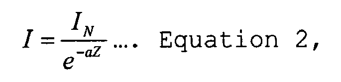
where I is an intensity of a laser beam irradiated, IN is an intensity of a laser beam necessary for decomposing a nitride layer, α is an absorption coefficient of a laser beam, and Z is a thickness of a buffer layer. - For example, on the assumption that a laser used for a laser lift off process is a Q-switched Nd:YAG laser having an absorption coefficient of about 105/cm and a wavelength of 355nm, and the
nitride layer 120 begins to be decomposed by a laser beam having an intensity of 300 mJ/cm2, in the case of a buffer layer with a thickness of 10nm, the laser beam is irradiated at an intensity of I=300/e-100000×0.000001332 mJ/cm2. As described above,
Equation 2 can be used to calculate the intensity of the laser beam that enables separation of thenitride layer 120 at the interface between thebuffer layer 110 and thenitride layer 120 as shown in FIG. 2d. - Further, the intensity of the laser beam can be adjusted according to
Equation 2 above to ensure separation of the nitride layer at the interface between abuffer layer 110 and anitride layer 120. In this case, heat generated in separating thenitride layer 120 is transferred to thebuffer layer 110 having a high thermal conductivity, thereby preventing quality degradation of thenitride layer 120 caused by thermal conduction into thenitride layer 120. - FIG. 3 is a graph illustrating an XPS analysis result for a separated surface of a nitride layer after a laser lift off process according to the invention. At this time, for a buffer layer, SiC was used, and the nitride layer was made of GaN. As shown in FIG. 3, elements such as C, O, N, Ga, Au, and the like were detected on the separated surface except for Si of the buffer layer. This demonstrates that the nitride layer was removed at an interface between the buffer layer and the nitride layer without decomposing the buffer layer made of SiC.
- FIG. 4 is a TEM picture illustrating a separated surface of the nitride layer after a laser lift off process according to the invention. As in FIG. 3, for the buffer layer, SiC was used and the nitride layer was made of GaN. As shown in FIG. 4, the lattice of GaN was clearly revealed on the separated surface of the nitride layer. This indicates that the nitride layer was removed at the interface between the buffer layer and the nitride layer without decomposing the buffer layer.
- The method for manufacturing the nitride layer according to the invention as described above may be employed to fabricate a bulk nitride substrate. In addition, the manufacturing method of the invention may be used to fabricate a vertical nitride semiconductor light emitting device that requires a process of removing a sapphire substrate. FIGs. 5a to 5f show a method for manufacturing a vertical nitride semiconductor light emitting device according to the invention.
- First, as shown in FIG. 5a, a
sapphire substrate 200 is prepared, and abuffer layer 210 made of SiC is formed on thesapphire substrate 200. The process of forming thebuffer layer 210 is the same as stated earlier and thus a detailed explanation thereof will not be given. - Thereafter, as shown in FIG. 5b, a
light emitting structure 220 having an n-typenitride semiconductor layer 221, anactive layer 222, and a p-typenitride semiconductor layer 223 stacked sequentially is formed on thebuffer layer 210. At this time, the n-typenitride semiconductor layer 221 has a composition expressed by AlxInyGa(1-x-y)N, where 0≤x≤1, 0≤y≤1, and 0≤x+y≤1. - The n-type
nitride semiconductor layer 221 is made of a semiconductor material doped with impurities of , for example, Si, Ge, Se, Te or C to have a composition expressed by AlxInyGa(1-x-y)N, where 0≤x≤1, 0≤y≤1, and 0≤x+y≤1. The n-typenitride semiconductor layer 221 can be grown on the sapphire substrate via a well-known deposition process such as Metal Organic Chemical Vapor Deposition (MOCVD), Molecular Beam Epitaxy (MBE) or Hybride Vapor Phase Epitaxy (HVPE). - The
active layer 222, through which light exits, is made of the nitride layer such as GaN or InGaN having a single or multiple quantum well structure. Like the n-typenitride semiconductor layer 221, theactive layer 222 is also formed on the n-type semiconductor layer via MOCVD, MBE or HVPE. - Like the n-type
nitride semiconductor layer 221, the p-typenitride semiconductor layer 223 is made of a semiconductor material p-doped with impurities of, for example, Mg, Zn, or Be to have a composition expressed by AlxInyGa(1-x-y)N, where 0≤x≤1, 0≤y≤1, and 0≤x+y≤1. The p-typenitride semiconductor layer 223 can be grown on theactive layer 222 via a well-known deposition process such as MOCVD, MBE or HVPE. - The
light emitting structure 220 may further include an undoped nitride semiconductor layer (not illustrated) that is formed on thebuffer layer 210 before the forming of the n-typenitride semiconductor layer 221. The undoped nitride semiconductor layer is formed to relieve lattice mismatch. - Next, as shown in FIG. 5c, a
conductive carrier substrate 230 is formed on the p-typenitride semiconductor layer 223. Theconductive carrier substrate 230 may be made of Si or a conductive metal material. Theconductive carrier substrate 230 may be bonded onto the p-typenitride semiconductor layer 223 via a separate adhesive layer or plated onto the p-typenitride semiconductor layer 223 to a predetermined thickness by using a platable metal material. In the case of the vertical nitride semiconductor light emitting device, a separated surface of the sapphire substrate in the n-typenitride semiconductor layer 221 is used as a surface where light exits. Therefore a reflective film made of a highly reflective metal may be formed between the p-typenitride semiconductor layer 223 and aconductive carrier substrate 230. - Thereafter, as shown in FIG. 5d, a laser beam is irradiated to an underside of the
sapphire substrate 200. This allows thelight emitting structure 220 to be separated from thebuffer layer 210 at an interface between thebuffer layer 210 and the n-typenitride semiconductor layer 221 so that a resultant structure of FIG. 5e is obtained. At this time, the laser beam is irradiated at an intensity according to Equation 2:
where I is an intensity of the irradiated laser beam, IN is an intensity of the laser beam required to partially decompose the n-type nitride semiconductor layer, α is an absorption coefficient of the laser beam, and Z is a thickness of the buffer layer. - An explanation will not be given regarding an intensity and a wavelength of the laser beam that ensures removal of the
light emitting structure 220 at the interface between the n-typenitride semiconductor layer 221 and thebuffer layer 210 since it has been described earlier with respect to the method for manufacturing the nitride layer. - Meanwhile, in case where the
light emitting structure 220 further includes an undoped nitride semiconductor layer (not illustrated) formed underlying the n-typenitride semiconductor layer 221, the separation by laser beam irradiation as described above will occur between thebuffer layer 210 and the undoped nitride semiconductor layer. - Thereafter, as in FIG. 5f, to complete the vertical nitride semiconductor light emitting device, an n-
electrode 240 is formed on an underside of the n-typenitride semiconductor layer 221 after the sapphire substrate is removed. Also, a p-type electrode 250 is formed on thecarrier substrate 230. In the vertical nitride semiconductor light emitting device, the underside of the n-typenitride semiconductor layer 221 with the sapphire substrate removed is used as a main light exiting surface. A transparent electrode layer made of ITO may be formed between the n-electrode 240 and the n-typenitride semiconductor layer 221 to improve current spread. Furthermore, in case where theconductive carrier substrate 230 is made of a metal material having excellent electrical conductivity, thecarrier substrate 230 itself may be employed as a p-electrode without any need to form a separate p-electrode 250. - In addition, in case where the
light emitting structure 220 further includes an undoped nitride semiconductor layer (not illustrated) formed underlying the n-typenitride semiconductor layer 221, the undoped nitride semiconductor layer, after separation of thelight emitting structure 220 by laser beam irradiation, is removed via at least one selected from a group consisting of dry-etching, wet-etching, chemical mechanical polishing (CMP) to expose the underside of the n-typenitride semiconductor layer 221. Then, preferably, the n-electrode is formed on the exposed underside of the n-typenitride semiconductor layer 221. - A laser lift off process adopted in the invention ensures a nitride layer to be removed at an interface between a nitride layer and a buffer layer by adjusting an intensity of a laser beam without sacrificing a buffer layer. This allows heat generated during partial decomposition of the nitride layer to exit through the buffer layer, preventing heat-induced degradation of the nitride layer and thus enabling manufacture of the high-quality nitride layer.
- As described above, according to the invention, a laser lift off process is employed to remove a sapphire substrate after growing a nitride layer on the sapphire substrate. In this process, an intensity of a laser beam irradiated is properly adjusted to ensure the separation to occur at an interface between the nitride layer and a buffer layer. Thereby, this advantageously allows heat generated during partial decomposition of the nitride layer to exit through the buffer layer, thus preventing heat-induced deterioration of the nitride layer. As a result, the invention advantageously enables manufacture of the high-quality nitride layer and vertical nitride semiconductor light emitting device.
- While the present invention has been shown and described in connection with the preferred embodiments, it will be apparent to those skilled in the art that modifications and variations can be made without departing from the spirit and scope of the invention as defined by the appended claims.
Claims (10)
- A method for fabricating a nitride layer comprising steps of:preparing a sapphire substrate;forming a buffer layer made of a material having a melting point and a thermal conductivity higher than those of nitride on the sapphire substrate;forming the nitride layer on the buffer layer; andirradiating a laser beam to an underside of the sapphire substrate to remove the nitride layer.
- The method according to claim 1, wherein the buffer layer has a thickness of 2000Å or less.
- The method according to claim 1, wherein the buffer layer comprises SiC.
- The method according to claim 1, wherein the nitride layer comprises a material having a composition expressed by AlxInyGa(1-x-y)N, where 0≤x≤1, 0≤y≤1, and 0≤x+y≤1.
- The method according to claim 1, wherein the laser beam irradiating step comprises: irradiating a laser beam having an intensity expressed by an equation below to the underside of the sapphire substrate to remove the nitride layer at an interface between the buffer layer and the nitride layer,

wherein I is an intensity of the irradiated laser beam, IN is an intensity of the laser beam required to partially decompose the nitride layer, a is an absorption coefficient of the laser beam, and Z is a thickness of the buffer layer. - A method for fabricating a nitride layer comprising steps of:preparing a sapphire substrate;forming a buffer layer made of SiC on the sapphire substrate;forming a nitride layer having a composition expressed by AlxInyGa(1-x-y)N on the buffer layer, where 0≤x≤1, 0≤y≤1, and 0≤x+y≤1; andirradiating a laser beam having an intensity expressed by an equation below to the sapphire substrate to remove the nitride layer at an interface between the buffer layer and the nitride layer,

wherein I is an intensity of the irradiated laser beam, IN is an intensity of the laser beam required to partially decompose the nitride layer, α is an absorption coefficient of the laser beam, and Z is a thickness of the buffer layer. - A method for fabricating a vertical nitride semiconductor light emitting device comprising steps of:preparing a sapphire substrate;forming a buffer layer made of SiC on the sapphire substrate;forming a light emitting structure having an n-type nitride semiconductor layer, an active layer, and a p-type nitride semiconductor layer stacked sequentially on the buffer layer, the n-type nitride semiconductor layer having a composition expressed by AlxInyGa (1-x-y) N, where 0≤x≤1, 0≤y≤1, and 0≤x+y≤1;providing a conductive carrier substrate on the p-type nitride semiconductor layer; andirradiating a laser beam having an intensity expressed by an equation below to an underside of the sapphire substrate to separate the light emitting structure from the sapphire substrate at an interface between the buffer layer and the light emitting structure,

wherein I is an intensity of the irradiated laser beam, IN is an intensity of the laser beam required to partially decompose the n-type nitride semiconductor layer, α is an absorption coefficient of the laser beam, and Z is a thickness of the buffer layer. - The method according to claim 7, further comprising:forming an n-electrode on an underside of the n-type nitride semiconductor layer after the sapphire substrate is removed; andforming a p-electrode on the carrier substrate.
- The method according to claim 7, wherein the light emitting structure further comprises an undoped nitride semiconductor layer formed underlying the n-type nitride semiconductor layer.
- The method according to claim 9, further comprising after the sapphire substrate removing step, removing the undoped nitride semiconductor layer via at least one selected from a group consisting of dry-etching, wet-etching and chemical mechanical polishing.
Applications Claiming Priority (1)
| Application Number | Priority Date | Filing Date | Title |
|---|---|---|---|
| KR1020050034351A KR100665173B1 (en) | 2005-04-26 | 2005-04-26 | Method of manufacturing nitride layer and method of manufacturing vertical nitride semiconductor light emitting device using same |
Publications (2)
| Publication Number | Publication Date |
|---|---|
| EP1717872A2 true EP1717872A2 (en) | 2006-11-02 |
| EP1717872A3 EP1717872A3 (en) | 2012-08-22 |
Family
ID=36685737
Family Applications (1)
| Application Number | Title | Priority Date | Filing Date |
|---|---|---|---|
| EP06252227A Withdrawn EP1717872A3 (en) | 2005-04-26 | 2006-04-26 | Method of producing nitride layer and method of fabricating vertical semiconductor light emitting device |
Country Status (4)
| Country | Link |
|---|---|
| US (1) | US7524692B2 (en) |
| EP (1) | EP1717872A3 (en) |
| JP (1) | JP4592636B2 (en) |
| KR (1) | KR100665173B1 (en) |
Families Citing this family (11)
| Publication number | Priority date | Publication date | Assignee | Title |
|---|---|---|---|---|
| JP2008294379A (en) * | 2007-05-28 | 2008-12-04 | Sanyo Electric Co Ltd | Manufacturing method of nitride-based semiconductor element |
| JP4599442B2 (en) | 2008-08-27 | 2010-12-15 | 株式会社東芝 | Manufacturing method of semiconductor light emitting device |
| CN101740331B (en) * | 2008-11-07 | 2012-01-25 | 东莞市中镓半导体科技有限公司 | Method for nondestructive stripping of GaN and sapphire substrate by using solid laser |
| KR101064068B1 (en) * | 2009-02-25 | 2011-09-08 | 엘지이노텍 주식회사 | Manufacturing method of light emitting device |
| WO2011069242A1 (en) * | 2009-12-09 | 2011-06-16 | Cooledge Lighting Inc. | Semiconductor dice transfer-enabling apparatus and method for manufacturing transfer-enabling apparatus |
| US20110151588A1 (en) * | 2009-12-17 | 2011-06-23 | Cooledge Lighting, Inc. | Method and magnetic transfer stamp for transferring semiconductor dice using magnetic transfer printing techniques |
| US8334152B2 (en) * | 2009-12-18 | 2012-12-18 | Cooledge Lighting, Inc. | Method of manufacturing transferable elements incorporating radiation enabled lift off for allowing transfer from host substrate |
| CN102064255A (en) * | 2010-12-10 | 2011-05-18 | 西安神光安瑞光电科技有限公司 | LED (Light Emitting Diode) and manufacturing method thereof |
| JP2013110137A (en) * | 2011-11-17 | 2013-06-06 | Disco Abrasive Syst Ltd | Optical device layer transfer device and laser processing machine |
| JP5521242B1 (en) * | 2013-06-08 | 2014-06-11 | エルシード株式会社 | SiC material manufacturing method and SiC material laminate |
| CN103824905A (en) * | 2014-02-24 | 2014-05-28 | 无锡晶凯科技有限公司 | Laser lift-off method for flexible electronic application of sapphire substrate of gallium nitride LED |
Family Cites Families (6)
| Publication number | Priority date | Publication date | Assignee | Title |
|---|---|---|---|---|
| US6649494B2 (en) * | 2001-01-29 | 2003-11-18 | Matsushita Electric Industrial Co., Ltd. | Manufacturing method of compound semiconductor wafer |
| WO2002103769A1 (en) * | 2001-06-18 | 2002-12-27 | Toyoda Gosei Co., Ltd. | P-type semiconductor manufacturing method and semiconductor device |
| JP3856750B2 (en) * | 2001-11-13 | 2006-12-13 | 松下電器産業株式会社 | Semiconductor device and manufacturing method thereof |
| CA2754097C (en) * | 2002-01-28 | 2013-12-10 | Nichia Corporation | Nitride semiconductor device having support substrate and its manufacturing method |
| KR101030068B1 (en) * | 2002-07-08 | 2011-04-19 | 니치아 카가쿠 고교 가부시키가이샤 | Nitride semiconductor device manufacturing method and nitride semiconductor device |
| JP4830315B2 (en) * | 2004-03-05 | 2011-12-07 | 日亜化学工業株式会社 | Semiconductor laser element |
-
2005
- 2005-04-26 KR KR1020050034351A patent/KR100665173B1/en not_active Expired - Fee Related
-
2006
- 2006-04-24 JP JP2006118962A patent/JP4592636B2/en not_active Expired - Lifetime
- 2006-04-25 US US11/410,052 patent/US7524692B2/en active Active
- 2006-04-26 EP EP06252227A patent/EP1717872A3/en not_active Withdrawn
Non-Patent Citations (1)
| Title |
|---|
| None * |
Also Published As
| Publication number | Publication date |
|---|---|
| JP2006310851A (en) | 2006-11-09 |
| US7524692B2 (en) | 2009-04-28 |
| EP1717872A3 (en) | 2012-08-22 |
| KR100665173B1 (en) | 2007-01-09 |
| KR20060112013A (en) | 2006-10-31 |
| US20060292718A1 (en) | 2006-12-28 |
| JP4592636B2 (en) | 2010-12-01 |
Similar Documents
| Publication | Publication Date | Title |
|---|---|---|
| JP5167384B2 (en) | Substrate dividing method | |
| US7760785B2 (en) | Group-III nitride semiconductor device | |
| KR101361630B1 (en) | Method for production a radiation-emitting semi-conductor chip | |
| KR101997416B1 (en) | Method for producing an optoelectronic semiconductor chip and optoelectronic semiconductor chip | |
| EP0551721A2 (en) | Gallium nitride base semiconductor device and method of fabricating the same | |
| US7524692B2 (en) | Method of producing nitride layer and method of fabricating vertical structure nitride semiconductor light emitting device | |
| US6797532B2 (en) | Semiconductor device and method for manufacturing the same | |
| EP2635726A1 (en) | Method of forming a composite substrate. | |
| JP2016058693A (en) | Semiconductor device, semiconductor wafer, and manufacturing method of semiconductor device | |
| CN116802349A (en) | Semiconductor substrate and manufacturing method, manufacturing device, electronic component and electronic equipment | |
| JP3803606B2 (en) | Method for manufacturing group III nitride semiconductor substrate | |
| US6881261B2 (en) | Method for fabricating semiconductor device | |
| EP1768194B1 (en) | Method of manufacturing nitride semiconductor device | |
| JP2003218052A (en) | Method for manufacturing semiconductor device | |
| KR20130008281A (en) | Methods for manufacturing power devices | |
| KR101058302B1 (en) | Thin film semiconductor device and method of manufacturing the device | |
| US9299561B2 (en) | Method for fabricating nitride semiconductor thin film and method for fabricating nitride semiconductor device using the same | |
| JP2014500842A (en) | Group III nitride layer grown on substrate | |
| KR101158077B1 (en) | High efficiency light emitting diode and method of fabricating the same | |
| US6432847B1 (en) | Method of activating P-type compound semiconductor by using lasers for reducing the resistivity thereof | |
| CN117178369A (en) | Semiconductor devices, electronic equipment and methods of forming semiconductor devices | |
| JP2006024909A (en) | Method for dividing substrate | |
| JP2007300146A (en) | Semiconductor device and manufacturing method thereof |
Legal Events
| Date | Code | Title | Description |
|---|---|---|---|
| PUAI | Public reference made under article 153(3) epc to a published international application that has entered the european phase |
Free format text: ORIGINAL CODE: 0009012 |
|
| AK | Designated contracting states |
Kind code of ref document: A2 Designated state(s): AT BE BG CH CY CZ DE DK EE ES FI FR GB GR HU IE IS IT LI LT LU LV MC NL PL PT RO SE SI SK TR |
|
| AX | Request for extension of the european patent |
Extension state: AL BA HR MK YU |
|
| RAP1 | Party data changed (applicant data changed or rights of an application transferred) |
Owner name: SAMSUNG LED CO., LTD. |
|
| PUAL | Search report despatched |
Free format text: ORIGINAL CODE: 0009013 |
|
| AK | Designated contracting states |
Kind code of ref document: A3 Designated state(s): AT BE BG CH CY CZ DE DK EE ES FI FR GB GR HU IE IS IT LI LT LU LV MC NL PL PT RO SE SI SK TR |
|
| AX | Request for extension of the european patent |
Extension state: AL BA HR MK YU |
|
| RIC1 | Information provided on ipc code assigned before grant |
Ipc: C30B 29/40 20060101ALI20120713BHEP Ipc: H01L 21/762 20060101ALI20120713BHEP Ipc: H01L 33/00 20100101AFI20120713BHEP Ipc: C30B 33/00 20060101ALI20120713BHEP |
|
| RAP1 | Party data changed (applicant data changed or rights of an application transferred) |
Owner name: SAMSUNG ELECTRONICS CO., LTD. |
|
| 17P | Request for examination filed |
Effective date: 20130206 |
|
| AKX | Designation fees paid |
Designated state(s): AT BE BG CH CY CZ DE DK EE ES FI FR GB GR HU IE IS IT LI LT LU LV MC NL PL PT RO SE SI SK TR |
|
| 17Q | First examination report despatched |
Effective date: 20170301 |
|
| STAA | Information on the status of an ep patent application or granted ep patent |
Free format text: STATUS: THE APPLICATION IS DEEMED TO BE WITHDRAWN |
|
| 18D | Application deemed to be withdrawn |
Effective date: 20170712 |