EP1716729B1 - Leiterplatte mit einer kartenleseeinrichtung - Google Patents
Leiterplatte mit einer kartenleseeinrichtung Download PDFInfo
- Publication number
- EP1716729B1 EP1716729B1 EP05716593A EP05716593A EP1716729B1 EP 1716729 B1 EP1716729 B1 EP 1716729B1 EP 05716593 A EP05716593 A EP 05716593A EP 05716593 A EP05716593 A EP 05716593A EP 1716729 B1 EP1716729 B1 EP 1716729B1
- Authority
- EP
- European Patent Office
- Prior art keywords
- circuit board
- printed circuit
- card
- reading device
- card reading
- Prior art date
- Legal status (The legal status is an assumption and is not a legal conclusion. Google has not performed a legal analysis and makes no representation as to the accuracy of the status listed.)
- Expired - Lifetime
Links
- 230000013011 mating Effects 0.000 description 2
Images


Classifications
-
- H—ELECTRICITY
- H05—ELECTRIC TECHNIQUES NOT OTHERWISE PROVIDED FOR
- H05K—PRINTED CIRCUITS; CASINGS OR CONSTRUCTIONAL DETAILS OF ELECTRIC APPARATUS; MANUFACTURE OF ASSEMBLAGES OF ELECTRICAL COMPONENTS
- H05K9/00—Screening of apparatus or components against electric or magnetic fields
- H05K9/0007—Casings
- H05K9/002—Casings with localised screening
- H05K9/0022—Casings with localised screening of components mounted on printed circuit boards [PCB]
- H05K9/0024—Shield cases mounted on a PCB, e.g. cans or caps or conformal shields
- H05K9/0032—Shield cases mounted on a PCB, e.g. cans or caps or conformal shields having multiple parts, e.g. frames mating with lids
-
- H—ELECTRICITY
- H04—ELECTRIC COMMUNICATION TECHNIQUE
- H04M—TELEPHONIC COMMUNICATION
- H04M1/00—Substation equipment, e.g. for use by subscribers
- H04M1/02—Constructional features of telephone sets
- H04M1/0202—Portable telephone sets, e.g. cordless phones, mobile phones or bar type handsets
-
- H—ELECTRICITY
- H04—ELECTRIC COMMUNICATION TECHNIQUE
- H04M—TELEPHONIC COMMUNICATION
- H04M2250/00—Details of telephonic subscriber devices
- H04M2250/14—Details of telephonic subscriber devices including a card reading device
Definitions
- the present invention relates to a printed circuit board having at least one card reading device, wherein the card reading device consists essentially of a receiving device for the card and contacts for reading or writing the card.
- card reading devices are arranged directly on the circuit board in the known printed circuit boards with card readers, one encounters in the miniaturization of devices, for example, from mobile phones, in which these boards are used, to limits.
- GB-A-2 269 940 shows a printed circuit board with a card reading device, wherein the card reading device consists essentially of a receiving device for the card and contacts for reading or writing the card and the receiving device is arranged on a shielding device of the circuit board, the contacts from the circuit board through the shielding device are guided.
- the object of the present invention is to provide a printed circuit board with an existing card reading device, in which, despite a card reading device more components can be accommodated on the circuit board.
- This object is achieved according to the invention for a printed circuit board of the type mentioned above in that the receiving device of a card reading device is arranged on a screen cover of a shielded module of the circuit board, and that the contacts are guided from the circuit board through the screen cover.
- the card reading device in order to integrate as many components as possible on the printed circuit board, the card reading device avoids a second level.
- the inventive system of printed circuit board and card reading device places the receiving device of the card reading device on a screen cover and thus represents a complete unit of frame, shield cover and card system. This opens up the possibility of the freed area For example, with other circuit board components to occupy.
- FIG. 1 schematically shows the structure of a printed circuit board 1 with a card reading device 4, 5, 6 according to the present invention.
- On the circuit board 1 are different components 2 arranged.
- Also arranged on the circuit board is a contact housing 6 which contains the contacts 5 for the card 3 to be read or written.
- the contacts 5, which connect mating contacts on the circuit board 1 with corresponding mating contacts on the card 3, are guided in an insulating contact housing 6.
- FIGS. 2 to 6 show an example of a practical embodiment of a printed circuit board with a card reading device according to the present invention.
- FIG. 2 shows the circuit board 1 with the contact housing 6 and several components to be shielded 2.
- FIG. 3 the part of the screen housing 7 forming screen frame 8 is applied to the circuit board 1.
- FIG. 4 shows the state when the screen cover 9 is mounted on the screen frame 8.
- the contacts 5 project through the screen cover 9 in order to come into contact with a card 3 to be inserted.
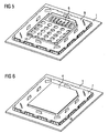
- FIG. 5 the state is shown in which on the screen cover 9, a frame 10 of a receiving device 4 is applied
- FIG. 6 shows a perspective view the printed circuit board 1 according to the invention with a card reading device 4 mounted on a screen housing 7.
Landscapes
- Engineering & Computer Science (AREA)
- Microelectronics & Electronic Packaging (AREA)
- Shielding Devices Or Components To Electric Or Magnetic Fields (AREA)
- Coupling Device And Connection With Printed Circuit (AREA)
- Selective Calling Equipment (AREA)
Description
- Die vorliegende Erfindung betrifft eine Leiterplatte mit mindestens einer Kartenleseeinrichtung, wobei die Kartenleseeinrichtung im Wesentlichen aus einer Aufnahmevorrichtung für die Karte und aus Kontakten zum Lesen bzw. Beschreiben der Karte besteht.
- Dadurch, dass bei den bekannten Leiterplatten mit Kartenleseeinrichtungen die Kartenleseeinrichtungen direkt auf der Leiterplatte angeordnet sind, stößt man bei der Miniaturisierung von Geräten, zum Beispiel von Mobiltelefonen, in welchen diese Leiterplatten eingesetzt sind, an Grenzen.
-
GB-A-2 269 940 - Aufgabe der vorliegenden Erfindung ist es, eine Leiterplatte mit einer vorhandenen Kartenleseeinrichtung anzugeben, bei welcher trotz einer Kartenleseeinrichtung mehr Bauteile auf der Leiterplatte untergebracht werden können.
- Diese Aufgabe wird erfindungsgemäß für eine Leiterplatte der eingangs genannten Art dadurch gelöst, dass die Aufnahmeeinrichtung einer Kartenleseeinrichtung auf einem Schirmdeckel einer abgeschirmten Baugruppe der Leiterplatte angeordnet ist, und dass die Kontakte von der Leiterplatte aus durch den Schirmdeckel geführt sind.
- Bei der erfindungsgemäßen Leiterplatte wird, um möglichst viele Bauteile auf der Leiterplatte zu integrieren, mit der Kartenleseeinrichtung auf eine zweite Ebene ausgewichen. Das erfindungsgemäße System aus Leiterplatte und Kartenleseeinrichtung platziert die Aufnahmeeinrichtung der Kartenleseeinrichtung auf einem Schirmdeckel und stellt somit eine komplette Einheit von Rahmen, Schirmdeckel und Kartensystem dar. Dadurch wird die Möglichkeit eröffnet, die frei werdende Fläche zum Beispiel mit weiteren Leiterplatten-Bauteile zu belegen.
- Die vorliegende Erfindung wird nachstehend anhand eines in der Zeichnung dargestellten Ausführungsbeispiels näher beschrieben.
- Es zeigen
-
Figur 1 einen schematischen Schnitt durch eine Leiterplatte mit einer Kartenleseeinrichtung gemäß der vorliegenden Erfindung, -
Figur 2 eine perspektivische Ansicht von oben auf eine Leiterplatte gemäß der vorliegenden Erfindung mit einem auf der Leiterplatte angebrachten Kontaktgehäuse für die Kartenleseeinrichtung und verschiedenen Bauteilen, -
Figur 3 eine perspektivische Ansicht von oben der inFigur 2 dargestellten Leiterplatte mit einem zusätzlich auf die Leiterplatte aufgebrachten Schirmrahmen, -
Figur 4 eine perspektivische Ansicht von oben der inFigur 2 und3 dargestellten Leiterplatte mit einem zusätzlich aufgebrachten Schirmdeckel, -
Figur 5 eine perspektivische Ansicht von oben der in den vorherigen Figuren dargestellten Leiterplatte mit einem aufgebrachten Kartenträgerrahmen, und -
Figur 6 eine perspektivische Ansicht von oben der in den vorherigen Figuren gezeigten Leiterplatte mit einer vollständigen Kartenleseeinrichtung. -
Figur 1 zeigt schematisch den Aufbau einer Leiterplatte 1 mit einer Kartenleseeinrichtung 4, 5, 6 gemäß der vorliegenden Erfindung. Auf der Leiterplatte 1 sind unterschiedliche Bauteile 2 angeordnet. Ebenfalls auf der Leiterplatte angeordnet ist ein Kontaktgehäuse 6, welches die Kontakte 5 für die zu lesende bzw. zu beschreibende Karte 3 enthält. Die Kontakte 5, welche Gegenkontakte auf der Leiterplatte 1 mit entsprechenden Gegenkontakten auf der Karte 3 verbinden, sind dabei in einem isolierenden Kontaktgehäuse 6 geführt. - Mehrere der Bauteile 2, welche das Kontaktgehäuse 6 umgeben, sind mittels eines Schirmgehäuses 7 abgeschirmt. Die Tatsache, dass bestimmte Bauteile 2 mittels eines Schirmgehäuses 2 elektrisch abgeschirmt werden müssen, macht sich die vorliegende Erfindung zu eigen, indem sie auf dem Schirmgehäuse 7, welches im Wesentlichen aus einem Schirmrahmen 8 und einem Schirmdeckel 9 besteht, die eigentliche Kartenaufnahmevorrichtung 4 für die Karte 3 anbringt, um auf diese Art und Weise die sonst für die Kartenleseeinrichtung verwendete Fläche auf der Leiterplatte 1 freizumachen.
- Die
Figuren 2 bis 6 zeigen ein Beispiel eines praktischen Ausführungsbeispiels einer Leiterplatte mit einer Kartenleseeinrichtung entsprechend der vorliegenden Erfindung. -
Figur 2 zeigt die Leiterplatte 1 mit dem Kontaktgehäuse 6 und mehreren zu schirmenden Bauteilen 2. InFigur 3 ist der ein Teil des Schirmgehäuses 7 bildende Schirmrahmen 8 auf die Leiterplatte 1 aufgebracht. -
Figur 4 zeigt den Zustand, wenn der Schirmdeckel 9 auf dem Schirmrahmen 8 befestigt ist. In dieser Darstellung lässt sich erkennen, dass die Kontakte 5 durch den Schirmdeckel 9 hindurchragen, um in Kontakt mit einer einzubringenden Karte 3 zu gelangen. - In
Figur 5 ist der Zustand gezeigt, in welchem auf dem Schirmdeckel 9 ein Rahmen 10 einer Aufnahmeeinrichtung 4 aufgebracht ist, undFigur 6 zeigt eine perspektivische Ansicht der erfindungsgemäßen Leiterplatte 1 mit einer auf ein Schirmgehäuse 7 aufgebrachten Kartenleseeinrichtung 4.
Claims (4)
- Leiterplatte mit mindestens einer Kartenleseeinrichtung, wobei die Kartenleseeinrichtung im Wesentlichen aus einer Aufnahmevorrichtung für die Karte und aus Kontakten zum Lesen bzw. Beschreiben der Karte besteht, wobei die Aufnahmeeinrichtung (4) der Kartenleseeinrichtung auf einem Schirmdeckel (9) einer abgeschirmten Baugruppe der Leiterplatte (1) angeordnet ist, und die Kontakte (5) von der Leiterplatte (1) aus durch den Schirmdeckel (9) geführt sind.
- Leiterplatte nach Anspruch 1, dadurch gekennzeichnet, dass die Kontakte (5) in einem auf der Leiterplatte (1) befestigten Kontaktgehäuse (6) geführt sind.
- Leiterplatte nach Anspruch 1 oder 2, dadurch gekennzeichnet, dass die Aufnahmeeinrichtung (4) einen Rahmen (10) aufweist, welcher mit dem Schirmdeckel (9) fest verbunden ist.
- Leiterplatte nach Anspruch 1 oder 2, dadurch gekennzeichnet, dass die Aufnahmeeinrichtung (4) einen Rahmen (10) aufweist, welcher mit dem Schirmdeckel (9) lösbar verbunden ist.
Applications Claiming Priority (2)
| Application Number | Priority Date | Filing Date | Title |
|---|---|---|---|
| DE102004007627A DE102004007627A1 (de) | 2004-02-17 | 2004-02-17 | Leiterplatte mit einer Kartenleseeinrichtung |
| PCT/EP2005/050305 WO2005081593A2 (de) | 2004-02-17 | 2005-01-25 | Leiterplatte mit einer kartenleseeinrichtung |
Publications (2)
| Publication Number | Publication Date |
|---|---|
| EP1716729A2 EP1716729A2 (de) | 2006-11-02 |
| EP1716729B1 true EP1716729B1 (de) | 2008-06-25 |
Family
ID=34832710
Family Applications (1)
| Application Number | Title | Priority Date | Filing Date |
|---|---|---|---|
| EP05716593A Expired - Lifetime EP1716729B1 (de) | 2004-02-17 | 2005-01-25 | Leiterplatte mit einer kartenleseeinrichtung |
Country Status (4)
| Country | Link |
|---|---|
| EP (1) | EP1716729B1 (de) |
| AT (1) | ATE399453T1 (de) |
| DE (2) | DE102004007627A1 (de) |
| WO (1) | WO2005081593A2 (de) |
Family Cites Families (4)
| Publication number | Priority date | Publication date | Assignee | Title |
|---|---|---|---|---|
| FI923694A7 (fi) * | 1992-08-18 | 1994-02-19 | Nokia Corp | Kortinlukijan suojaus |
| US5724234A (en) * | 1996-05-02 | 1998-03-03 | Ericsson Inc. | Slotted shield can |
| DE29811425U1 (de) * | 1998-06-29 | 1998-09-17 | Stocko Metallwarenfabriken Henkels & Sohn GmbH & Co, 42327 Wuppertal | Kontaktiereinheit für ein kartenförmiges Trägerelement elektronischer Baugruppen, insbesondere nach PCMCIA-Norm |
| DE19925146C2 (de) * | 1999-06-02 | 2003-01-09 | Itt Mfg Enterprises Inc | Steckkarte für elektronische Geräte |
-
2004
- 2004-02-17 DE DE102004007627A patent/DE102004007627A1/de not_active Ceased
-
2005
- 2005-01-25 EP EP05716593A patent/EP1716729B1/de not_active Expired - Lifetime
- 2005-01-25 DE DE502005004523T patent/DE502005004523D1/de not_active Expired - Fee Related
- 2005-01-25 WO PCT/EP2005/050305 patent/WO2005081593A2/de not_active Ceased
- 2005-01-25 AT AT05716593T patent/ATE399453T1/de not_active IP Right Cessation
Also Published As
| Publication number | Publication date |
|---|---|
| DE102004007627A1 (de) | 2005-09-08 |
| WO2005081593A3 (de) | 2005-11-10 |
| DE502005004523D1 (de) | 2008-08-07 |
| ATE399453T1 (de) | 2008-07-15 |
| WO2005081593A2 (de) | 2005-09-01 |
| EP1716729A2 (de) | 2006-11-02 |
Similar Documents
| Publication | Publication Date | Title |
|---|---|---|
| EP0735507A2 (de) | Kontaktiereinheit für kartenförmige Trägerelemente | |
| CH661816A5 (de) | Traeger mit einem ic-baustein. | |
| DE60037791T2 (de) | Karten-verbinder | |
| EP1816583A1 (de) | Kontaktiervorrichtung für eine Chipkarte | |
| DE4326029C2 (de) | Leser für Informationskarten | |
| DE69627818T2 (de) | Abgeschirmter speicherkartensteckverbinder | |
| DE69400397T2 (de) | Vorrichtung zur Schirmung und/oder Kühlung den elektronischen Komponenten | |
| EP1924947A1 (de) | Manipulations- und durchbohrschutz für eine an eine elektrische schaltung anzuschliessende vorrichtung | |
| EP2000945A1 (de) | Manipulationsgeschützter Kartenleser | |
| DE60221786T2 (de) | Steckverbinder geringer Höhe für eine USB-Schnittstelle und dazugehöriges Speichergerät | |
| EP1873680A1 (de) | Manipulationsgeschützter Kartenleser | |
| DE69626945T2 (de) | Aktiver Steckverbinder für Chipkarte | |
| DE69807312T2 (de) | Chipkartenleser | |
| DE69825962T2 (de) | Elektrischer Verbinder für das Kooperieren mit einem entfernbaren elektronischen Medium | |
| DE19925146A1 (de) | Steckkarte für elektronische Geräte | |
| EP1237395A1 (de) | Leiterplattenanordnung | |
| EP0189529B1 (de) | Mehretagiger Leiterplatten-Klemmenblock | |
| EP1716729A2 (de) | Leiterplatte mit einer kartenleseeinrichtung | |
| EP1785911A1 (de) | Kartenleser mit leiterbahnstrukturierter Kunststoffabdeckung | |
| EP1058202A3 (de) | Doppel-SIM-Kartenleser | |
| DE10032339A1 (de) | Vorrichtung und Brückenkarte für einen Computer | |
| DE20300687U1 (de) | Kartensteckverbinder mit integriertem Steuer-IC | |
| DE69114784T2 (de) | Anschlussaufbau für Karten mit integriertem Schaltkreis. | |
| DE102019132781A1 (de) | Störstrahlungsbund (EMI-Bund) zur Verwendung in einer Kraftfahrzeuganwendung | |
| WO2000006023A1 (de) | Biometrische sensoreinrichtung mit in einem flexleiterband integrierten elektronischen bauelementen |
Legal Events
| Date | Code | Title | Description |
|---|---|---|---|
| PUAI | Public reference made under article 153(3) epc to a published international application that has entered the european phase |
Free format text: ORIGINAL CODE: 0009012 |
|
| 17P | Request for examination filed |
Effective date: 20060706 |
|
| AK | Designated contracting states |
Kind code of ref document: A2 Designated state(s): AT BE BG CH CY CZ DE DK EE ES FI FR GB GR HU IE IS IT LI LT LU MC NL PL PT RO SE SI SK TR |
|
| GRAP | Despatch of communication of intention to grant a patent |
Free format text: ORIGINAL CODE: EPIDOSNIGR1 |
|
| DAX | Request for extension of the european patent (deleted) | ||
| 19U | Interruption of proceedings before grant |
Effective date: 20070101 |
|
| 19W | Proceedings resumed before grant after interruption of proceedings |
Effective date: 20071130 |
|
| GRAC | Information related to communication of intention to grant a patent modified |
Free format text: ORIGINAL CODE: EPIDOSCIGR1 |
|
| GRAJ | Information related to disapproval of communication of intention to grant by the applicant or resumption of examination proceedings by the epo deleted |
Free format text: ORIGINAL CODE: EPIDOSDIGR1 |
|
| GRAP | Despatch of communication of intention to grant a patent |
Free format text: ORIGINAL CODE: EPIDOSNIGR1 |
|
| GRAC | Information related to communication of intention to grant a patent modified |
Free format text: ORIGINAL CODE: EPIDOSCIGR1 |
|
| RAP1 | Party data changed (applicant data changed or rights of an application transferred) |
Owner name: BENQ CORPORATION |
|
| GRAS | Grant fee paid |
Free format text: ORIGINAL CODE: EPIDOSNIGR3 |
|
| GRAA | (expected) grant |
Free format text: ORIGINAL CODE: 0009210 |
|
| AK | Designated contracting states |
Kind code of ref document: B1 Designated state(s): AT BE BG CH CY CZ DE DK EE ES FI FR GB GR HU IE IS IT LI LT LU MC NL PL PT RO SE SI SK TR |
|
| REG | Reference to a national code |
Ref country code: GB Ref legal event code: FG4D Free format text: NOT ENGLISH |
|
| REG | Reference to a national code |
Ref country code: CH Ref legal event code: EP |
|
| REF | Corresponds to: |
Ref document number: 502005004523 Country of ref document: DE Date of ref document: 20080807 Kind code of ref document: P |
|
| REG | Reference to a national code |
Ref country code: IE Ref legal event code: FG4D Free format text: LANGUAGE OF EP DOCUMENT: GERMAN |
|
| PG25 | Lapsed in a contracting state [announced via postgrant information from national office to epo] |
Ref country code: SI Free format text: LAPSE BECAUSE OF FAILURE TO SUBMIT A TRANSLATION OF THE DESCRIPTION OR TO PAY THE FEE WITHIN THE PRESCRIBED TIME-LIMIT Effective date: 20080625 Ref country code: FI Free format text: LAPSE BECAUSE OF FAILURE TO SUBMIT A TRANSLATION OF THE DESCRIPTION OR TO PAY THE FEE WITHIN THE PRESCRIBED TIME-LIMIT Effective date: 20080625 |
|
| PG25 | Lapsed in a contracting state [announced via postgrant information from national office to epo] |
Ref country code: PL Free format text: LAPSE BECAUSE OF FAILURE TO SUBMIT A TRANSLATION OF THE DESCRIPTION OR TO PAY THE FEE WITHIN THE PRESCRIBED TIME-LIMIT Effective date: 20080625 Ref country code: NL Free format text: LAPSE BECAUSE OF FAILURE TO SUBMIT A TRANSLATION OF THE DESCRIPTION OR TO PAY THE FEE WITHIN THE PRESCRIBED TIME-LIMIT Effective date: 20080625 |
|
| NLV1 | Nl: lapsed or annulled due to failure to fulfill the requirements of art. 29p and 29m of the patents act | ||
| PG25 | Lapsed in a contracting state [announced via postgrant information from national office to epo] |
Ref country code: IS Free format text: LAPSE BECAUSE OF FAILURE TO SUBMIT A TRANSLATION OF THE DESCRIPTION OR TO PAY THE FEE WITHIN THE PRESCRIBED TIME-LIMIT Effective date: 20081025 Ref country code: CZ Free format text: LAPSE BECAUSE OF FAILURE TO SUBMIT A TRANSLATION OF THE DESCRIPTION OR TO PAY THE FEE WITHIN THE PRESCRIBED TIME-LIMIT Effective date: 20080625 Ref country code: LT Free format text: LAPSE BECAUSE OF FAILURE TO SUBMIT A TRANSLATION OF THE DESCRIPTION OR TO PAY THE FEE WITHIN THE PRESCRIBED TIME-LIMIT Effective date: 20080625 Ref country code: SE Free format text: LAPSE BECAUSE OF FAILURE TO SUBMIT A TRANSLATION OF THE DESCRIPTION OR TO PAY THE FEE WITHIN THE PRESCRIBED TIME-LIMIT Effective date: 20080925 |
|
| REG | Reference to a national code |
Ref country code: IE Ref legal event code: FD4D |
|
| PG25 | Lapsed in a contracting state [announced via postgrant information from national office to epo] |
Ref country code: PT Free format text: LAPSE BECAUSE OF FAILURE TO SUBMIT A TRANSLATION OF THE DESCRIPTION OR TO PAY THE FEE WITHIN THE PRESCRIBED TIME-LIMIT Effective date: 20081125 Ref country code: RO Free format text: LAPSE BECAUSE OF FAILURE TO SUBMIT A TRANSLATION OF THE DESCRIPTION OR TO PAY THE FEE WITHIN THE PRESCRIBED TIME-LIMIT Effective date: 20080625 Ref country code: ES Free format text: LAPSE BECAUSE OF FAILURE TO SUBMIT A TRANSLATION OF THE DESCRIPTION OR TO PAY THE FEE WITHIN THE PRESCRIBED TIME-LIMIT Effective date: 20081006 Ref country code: SK Free format text: LAPSE BECAUSE OF FAILURE TO SUBMIT A TRANSLATION OF THE DESCRIPTION OR TO PAY THE FEE WITHIN THE PRESCRIBED TIME-LIMIT Effective date: 20080625 |
|
| PG25 | Lapsed in a contracting state [announced via postgrant information from national office to epo] |
Ref country code: IE Free format text: LAPSE BECAUSE OF FAILURE TO SUBMIT A TRANSLATION OF THE DESCRIPTION OR TO PAY THE FEE WITHIN THE PRESCRIBED TIME-LIMIT Effective date: 20080625 Ref country code: BG Free format text: LAPSE BECAUSE OF FAILURE TO SUBMIT A TRANSLATION OF THE DESCRIPTION OR TO PAY THE FEE WITHIN THE PRESCRIBED TIME-LIMIT Effective date: 20080925 Ref country code: EE Free format text: LAPSE BECAUSE OF FAILURE TO SUBMIT A TRANSLATION OF THE DESCRIPTION OR TO PAY THE FEE WITHIN THE PRESCRIBED TIME-LIMIT Effective date: 20080625 Ref country code: DK Free format text: LAPSE BECAUSE OF FAILURE TO SUBMIT A TRANSLATION OF THE DESCRIPTION OR TO PAY THE FEE WITHIN THE PRESCRIBED TIME-LIMIT Effective date: 20080625 |
|
| PLBE | No opposition filed within time limit |
Free format text: ORIGINAL CODE: 0009261 |
|
| STAA | Information on the status of an ep patent application or granted ep patent |
Free format text: STATUS: NO OPPOSITION FILED WITHIN TIME LIMIT |
|
| PGFP | Annual fee paid to national office [announced via postgrant information from national office to epo] |
Ref country code: DE Payment date: 20090129 Year of fee payment: 5 |
|
| 26N | No opposition filed |
Effective date: 20090326 |
|
| PGFP | Annual fee paid to national office [announced via postgrant information from national office to epo] |
Ref country code: GB Payment date: 20090123 Year of fee payment: 5 |
|
| PG25 | Lapsed in a contracting state [announced via postgrant information from national office to epo] |
Ref country code: MC Free format text: LAPSE BECAUSE OF NON-PAYMENT OF DUE FEES Effective date: 20090131 |
|
| PGFP | Annual fee paid to national office [announced via postgrant information from national office to epo] |
Ref country code: IT Payment date: 20090126 Year of fee payment: 5 |
|
| REG | Reference to a national code |
Ref country code: CH Ref legal event code: PL |
|
| PG25 | Lapsed in a contracting state [announced via postgrant information from national office to epo] |
Ref country code: LI Free format text: LAPSE BECAUSE OF NON-PAYMENT OF DUE FEES Effective date: 20090131 Ref country code: CH Free format text: LAPSE BECAUSE OF NON-PAYMENT OF DUE FEES Effective date: 20090131 |
|
| PGFP | Annual fee paid to national office [announced via postgrant information from national office to epo] |
Ref country code: FR Payment date: 20090120 Year of fee payment: 5 |
|
| PG25 | Lapsed in a contracting state [announced via postgrant information from national office to epo] |
Ref country code: BE Free format text: LAPSE BECAUSE OF NON-PAYMENT OF DUE FEES Effective date: 20090131 |
|
| PG25 | Lapsed in a contracting state [announced via postgrant information from national office to epo] |
Ref country code: AT Free format text: LAPSE BECAUSE OF NON-PAYMENT OF DUE FEES Effective date: 20090125 |
|
| GBPC | Gb: european patent ceased through non-payment of renewal fee |
Effective date: 20100125 |
|
| REG | Reference to a national code |
Ref country code: FR Ref legal event code: ST Effective date: 20100930 |
|
| PG25 | Lapsed in a contracting state [announced via postgrant information from national office to epo] |
Ref country code: GR Free format text: LAPSE BECAUSE OF FAILURE TO SUBMIT A TRANSLATION OF THE DESCRIPTION OR TO PAY THE FEE WITHIN THE PRESCRIBED TIME-LIMIT Effective date: 20080926 Ref country code: FR Free format text: LAPSE BECAUSE OF NON-PAYMENT OF DUE FEES Effective date: 20100201 |
|
| PG25 | Lapsed in a contracting state [announced via postgrant information from national office to epo] |
Ref country code: DE Free format text: LAPSE BECAUSE OF NON-PAYMENT OF DUE FEES Effective date: 20100803 |
|
| PG25 | Lapsed in a contracting state [announced via postgrant information from national office to epo] |
Ref country code: GB Free format text: LAPSE BECAUSE OF NON-PAYMENT OF DUE FEES Effective date: 20100125 |
|
| PG25 | Lapsed in a contracting state [announced via postgrant information from national office to epo] |
Ref country code: IT Free format text: LAPSE BECAUSE OF NON-PAYMENT OF DUE FEES Effective date: 20100125 |
|
| PG25 | Lapsed in a contracting state [announced via postgrant information from national office to epo] |
Ref country code: LU Free format text: LAPSE BECAUSE OF NON-PAYMENT OF DUE FEES Effective date: 20090125 |
|
| PG25 | Lapsed in a contracting state [announced via postgrant information from national office to epo] |
Ref country code: HU Free format text: LAPSE BECAUSE OF FAILURE TO SUBMIT A TRANSLATION OF THE DESCRIPTION OR TO PAY THE FEE WITHIN THE PRESCRIBED TIME-LIMIT Effective date: 20081226 |
|
| PG25 | Lapsed in a contracting state [announced via postgrant information from national office to epo] |
Ref country code: TR Free format text: LAPSE BECAUSE OF FAILURE TO SUBMIT A TRANSLATION OF THE DESCRIPTION OR TO PAY THE FEE WITHIN THE PRESCRIBED TIME-LIMIT Effective date: 20080625 |
|
| PG25 | Lapsed in a contracting state [announced via postgrant information from national office to epo] |
Ref country code: CY Free format text: LAPSE BECAUSE OF FAILURE TO SUBMIT A TRANSLATION OF THE DESCRIPTION OR TO PAY THE FEE WITHIN THE PRESCRIBED TIME-LIMIT Effective date: 20080625 |