EP1713149A1 - Glaze soldered laser components and method of manufacturing - Google Patents
Glaze soldered laser components and method of manufacturing Download PDFInfo
- Publication number
- EP1713149A1 EP1713149A1 EP06251719A EP06251719A EP1713149A1 EP 1713149 A1 EP1713149 A1 EP 1713149A1 EP 06251719 A EP06251719 A EP 06251719A EP 06251719 A EP06251719 A EP 06251719A EP 1713149 A1 EP1713149 A1 EP 1713149A1
- Authority
- EP
- European Patent Office
- Prior art keywords
- glaze
- sections
- laser
- components
- section
- Prior art date
- Legal status (The legal status is an assumption and is not a legal conclusion. Google has not performed a legal analysis and makes no representation as to the accuracy of the status listed.)
- Granted
Links
- 238000004519 manufacturing process Methods 0.000 title description 3
- 239000000463 material Substances 0.000 claims abstract description 29
- 239000013078 crystal Substances 0.000 claims abstract description 28
- 239000000919 ceramic Substances 0.000 claims abstract description 27
- 230000005496 eutectics Effects 0.000 claims abstract description 10
- 238000005304 joining Methods 0.000 claims abstract description 7
- 230000031700 light absorption Effects 0.000 claims abstract description 7
- 230000004927 fusion Effects 0.000 claims abstract description 6
- 238000005476 soldering Methods 0.000 abstract description 25
- 238000000034 method Methods 0.000 abstract description 24
- 238000010304 firing Methods 0.000 abstract description 13
- 229910000679 solder Inorganic materials 0.000 abstract description 8
- 230000008569 process Effects 0.000 abstract description 6
- 239000000306 component Substances 0.000 description 45
- 239000011162 core material Substances 0.000 description 26
- 238000005253 cladding Methods 0.000 description 12
- 238000009792 diffusion process Methods 0.000 description 10
- 238000002844 melting Methods 0.000 description 10
- 230000008018 melting Effects 0.000 description 7
- 229910052594 sapphire Inorganic materials 0.000 description 7
- 239000010980 sapphire Substances 0.000 description 7
- 230000003287 optical effect Effects 0.000 description 6
- 238000000151 deposition Methods 0.000 description 5
- 239000011521 glass Substances 0.000 description 5
- 210000001503 joint Anatomy 0.000 description 5
- 239000002131 composite material Substances 0.000 description 4
- 238000013461 design Methods 0.000 description 4
- 238000005498 polishing Methods 0.000 description 4
- 239000000843 powder Substances 0.000 description 4
- 238000012545 processing Methods 0.000 description 4
- 239000002002 slurry Substances 0.000 description 4
- 238000012986 modification Methods 0.000 description 3
- 230000004048 modification Effects 0.000 description 3
- XLYOFNOQVPJJNP-UHFFFAOYSA-N water Substances O XLYOFNOQVPJJNP-UHFFFAOYSA-N 0.000 description 3
- 229910002796 Si–Al Inorganic materials 0.000 description 2
- JNDMLEXHDPKVFC-UHFFFAOYSA-N aluminum;oxygen(2-);yttrium(3+) Chemical compound [O-2].[O-2].[O-2].[Al+3].[Y+3] JNDMLEXHDPKVFC-UHFFFAOYSA-N 0.000 description 2
- 239000008358 core component Substances 0.000 description 2
- 230000008021 deposition Effects 0.000 description 2
- 238000010586 diagram Methods 0.000 description 2
- 238000002156 mixing Methods 0.000 description 2
- 230000009467 reduction Effects 0.000 description 2
- 239000007787 solid Substances 0.000 description 2
- 229910052596 spinel Inorganic materials 0.000 description 2
- 239000011029 spinel Substances 0.000 description 2
- 230000008646 thermal stress Effects 0.000 description 2
- 229910019901 yttrium aluminum garnet Inorganic materials 0.000 description 2
- 229910052779 Neodymium Inorganic materials 0.000 description 1
- 229910052769 Ytterbium Inorganic materials 0.000 description 1
- 230000001464 adherent effect Effects 0.000 description 1
- 230000003466 anti-cipated effect Effects 0.000 description 1
- 238000013459 approach Methods 0.000 description 1
- 230000015572 biosynthetic process Effects 0.000 description 1
- 229910010293 ceramic material Inorganic materials 0.000 description 1
- 230000001010 compromised effect Effects 0.000 description 1
- 238000001816 cooling Methods 0.000 description 1
- 238000005336 cracking Methods 0.000 description 1
- 230000007547 defect Effects 0.000 description 1
- 230000032798 delamination Effects 0.000 description 1
- 238000011161 development Methods 0.000 description 1
- 230000018109 developmental process Effects 0.000 description 1
- 238000004031 devitrification Methods 0.000 description 1
- 238000004090 dissolution Methods 0.000 description 1
- 230000000694 effects Effects 0.000 description 1
- 238000005538 encapsulation Methods 0.000 description 1
- 238000005516 engineering process Methods 0.000 description 1
- 238000010438 heat treatment Methods 0.000 description 1
- 230000002706 hydrostatic effect Effects 0.000 description 1
- 230000003993 interaction Effects 0.000 description 1
- 239000004973 liquid crystal related substance Substances 0.000 description 1
- 229910052751 metal Inorganic materials 0.000 description 1
- 239000002184 metal Substances 0.000 description 1
- 238000013508 migration Methods 0.000 description 1
- 230000005012 migration Effects 0.000 description 1
- 239000000203 mixture Substances 0.000 description 1
- QEFYFXOXNSNQGX-UHFFFAOYSA-N neodymium atom Chemical compound [Nd] QEFYFXOXNSNQGX-UHFFFAOYSA-N 0.000 description 1
- 230000010355 oscillation Effects 0.000 description 1
- 229910052574 oxide ceramic Inorganic materials 0.000 description 1
- 239000011224 oxide ceramic Substances 0.000 description 1
- 230000003071 parasitic effect Effects 0.000 description 1
- 230000002093 peripheral effect Effects 0.000 description 1
- 238000010791 quenching Methods 0.000 description 1
- 230000000171 quenching effect Effects 0.000 description 1
- 238000007789 sealing Methods 0.000 description 1
- 239000007790 solid phase Substances 0.000 description 1
- 238000009718 spray deposition Methods 0.000 description 1
- 230000035882 stress Effects 0.000 description 1
- 229910019655 synthetic inorganic crystalline material Inorganic materials 0.000 description 1
- 238000012546 transfer Methods 0.000 description 1
- NAWDYIZEMPQZHO-UHFFFAOYSA-N ytterbium Chemical compound [Yb] NAWDYIZEMPQZHO-UHFFFAOYSA-N 0.000 description 1
Images


Classifications
-
- H—ELECTRICITY
- H01—ELECTRIC ELEMENTS
- H01S—DEVICES USING THE PROCESS OF LIGHT AMPLIFICATION BY STIMULATED EMISSION OF RADIATION [LASER] TO AMPLIFY OR GENERATE LIGHT; DEVICES USING STIMULATED EMISSION OF ELECTROMAGNETIC RADIATION IN WAVE RANGES OTHER THAN OPTICAL
- H01S3/00—Lasers, i.e. devices using stimulated emission of electromagnetic radiation in the infrared, visible or ultraviolet wave range
- H01S3/05—Construction or shape of optical resonators; Accommodation of active medium therein; Shape of active medium
- H01S3/06—Construction or shape of active medium
- H01S3/0602—Crystal lasers or glass lasers
-
- H—ELECTRICITY
- H01—ELECTRIC ELEMENTS
- H01S—DEVICES USING THE PROCESS OF LIGHT AMPLIFICATION BY STIMULATED EMISSION OF RADIATION [LASER] TO AMPLIFY OR GENERATE LIGHT; DEVICES USING STIMULATED EMISSION OF ELECTROMAGNETIC RADIATION IN WAVE RANGES OTHER THAN OPTICAL
- H01S3/00—Lasers, i.e. devices using stimulated emission of electromagnetic radiation in the infrared, visible or ultraviolet wave range
- H01S3/05—Construction or shape of optical resonators; Accommodation of active medium therein; Shape of active medium
- H01S3/06—Construction or shape of active medium
- H01S3/0602—Crystal lasers or glass lasers
- H01S3/0606—Crystal lasers or glass lasers with polygonal cross-section, e.g. slab, prism
-
- H—ELECTRICITY
- H01—ELECTRIC ELEMENTS
- H01S—DEVICES USING THE PROCESS OF LIGHT AMPLIFICATION BY STIMULATED EMISSION OF RADIATION [LASER] TO AMPLIFY OR GENERATE LIGHT; DEVICES USING STIMULATED EMISSION OF ELECTROMAGNETIC RADIATION IN WAVE RANGES OTHER THAN OPTICAL
- H01S3/00—Lasers, i.e. devices using stimulated emission of electromagnetic radiation in the infrared, visible or ultraviolet wave range
- H01S3/05—Construction or shape of optical resonators; Accommodation of active medium therein; Shape of active medium
- H01S3/06—Construction or shape of active medium
- H01S3/0602—Crystal lasers or glass lasers
- H01S3/0612—Non-homogeneous structure
-
- H—ELECTRICITY
- H01—ELECTRIC ELEMENTS
- H01S—DEVICES USING THE PROCESS OF LIGHT AMPLIFICATION BY STIMULATED EMISSION OF RADIATION [LASER] TO AMPLIFY OR GENERATE LIGHT; DEVICES USING STIMULATED EMISSION OF ELECTROMAGNETIC RADIATION IN WAVE RANGES OTHER THAN OPTICAL
- H01S3/00—Lasers, i.e. devices using stimulated emission of electromagnetic radiation in the infrared, visible or ultraviolet wave range
- H01S3/14—Lasers, i.e. devices using stimulated emission of electromagnetic radiation in the infrared, visible or ultraviolet wave range characterised by the material used as the active medium
- H01S3/16—Solid materials
- H01S3/1601—Solid materials characterised by an active (lasing) ion
- H01S3/1603—Solid materials characterised by an active (lasing) ion rare earth
- H01S3/1618—Solid materials characterised by an active (lasing) ion rare earth ytterbium
-
- H—ELECTRICITY
- H01—ELECTRIC ELEMENTS
- H01S—DEVICES USING THE PROCESS OF LIGHT AMPLIFICATION BY STIMULATED EMISSION OF RADIATION [LASER] TO AMPLIFY OR GENERATE LIGHT; DEVICES USING STIMULATED EMISSION OF ELECTROMAGNETIC RADIATION IN WAVE RANGES OTHER THAN OPTICAL
- H01S3/00—Lasers, i.e. devices using stimulated emission of electromagnetic radiation in the infrared, visible or ultraviolet wave range
- H01S3/14—Lasers, i.e. devices using stimulated emission of electromagnetic radiation in the infrared, visible or ultraviolet wave range characterised by the material used as the active medium
- H01S3/16—Solid materials
- H01S3/163—Solid materials characterised by a crystal matrix
- H01S3/164—Solid materials characterised by a crystal matrix garnet
- H01S3/1643—YAG
Definitions
- the present invention relates to solid-state laser technology. More specifically, the present invention relates to techniques and materials for joining laser components.
- Solid-state laser slabs typically include a thin planar solid-state gain medium (core plate) that is encapsulated by a solid crystal cladding.
- the core plate primarily having a rectangular cross-section, is a key laser component affecting beam quality at high energy levels.
- Yb:YAG ytterbium doped yttrium-aluminum-garnet
- Nd:YAG neodymium doped yttrium-aluminum-garnet
- polycrystalline transparent ceramics such as Y 3 A 15 O 12 .
- the core plate often includes two undoped input and output sections bonded to a doped central section.
- the bonded core is then structurally integrated with a peripheral crystal plate cladding made from material (such as Sapphire, Spinel, or related ceramics) having a step-index refractivity interface with the core to suppress parasitic oscillations that deplete energy in the core gain medium.
- a laser slab may also include various prisms joined to the input and output sections for inserting pump light and extracting laser energy from the slab.
- Diffusion bonding typically includes placing the joining crystal or ceramic units in intimate contact and applying external pressure and heat, so the units can be bonded together uniformly throughout.
- the pressure and temperature can be constant or variable, including various programmable cycles.
- Various pressurization techniques include those using "hot presses", hydrostatic systems, statically indeterminate systems (which develop intrinsic thermal stresses when heated), and the techniques based on van der Vaals force-assisted optical contacting. All these pressurization techniques, as well as precision grinding and polishing, are commonly used in the fabrication of core components.
- Diffusion bonding of laser components meets enormous difficulties, particularly when bonding dissimilar materials such as YAG and Sapphire.
- the thermal (CTE) mismatch and high temperature processing (about 1200-1700 °C), as well as the high elastic moduli of Sapphire and YAG, result in high interfacial thermal stresses localized at the slab ends.
- the crystal dissimilarity (hexagonal vs. cubic) and lattice mismatch between Sapphire and YAG substantially complicate the solid phase interaction between the dissimilar crystals.
- Glass soldering is a well-known technique widely used in electronics and micro-optics for sealing of cathode tubes, liquid crystal displays, micro-optic components, hermetic encapsulation of glass and metal electronic packages, etc. Glass soldering typically uses high temperature melting glasses. In spite of the existing popularity of glass soldering, its application for laser components meets substantial limitations, primarily associated with the high temperature processing, which causes a haze appearance in YAG and increases its light absorption and scattering.
- the need in the art is addressed by the glaze soldered solid-state laser active medium of the present invention.
- the novel laser active medium includes a first section of a first material, a second section of a second material, and a layer of ceramic glaze joining the two sections.
- the first and second materials may be identical, similar, or dissimilar, and may include crystals or ceramics.
- the glaze is a multi-oxide eutectic ceramic glaze having a refractivity, light absorption, thermal expansion, and fusion temperature that are compatible with the adherent materials.
- the sections are joined using a novel glaze soldering process that includes the steps of positioning the sections, applying the ceramic glaze between the sections, and firing the glaze to solder the sections together.
- a laser component typically includes a plurality of sections including a doped central core, undoped input and output sections, cladding, and various attached prisms.
- Figs. 1-3 show a few example laser component configurations.
- Fig. 1a is a perspective view of a conventional laser slab 10
- Fig. 1b is a side view of the conventional laser slab 10 of Fig. 1a.
- the laser slab 10 is comprised of a thin core plate having a rectangular cross-section and including a doped central section 12, an undoped input section 14, and an undoped output section 16.
- the core solid-state gain medium
- the core can be made from single crystals such as Yb:YAG and Nd:YAG, or from similar oxides in the form of nano-crystalline and fully transparent ceramics, or from combinations of crystals and ceramic sections. Diffusion bonding is typically used to bond these sections.
- Fig. 2 is a cross-sectional view of a laser slab 20 with conventional plate cladding.
- the laser slab 20 includes a Yb:YAG/YAG crystal composite core plate 10 that is peripherally encapsulated by solid Sapphire cladding plates 22.
- the cladding plates 22 are attached to the core plate 10 using conventional diffusion bonding.
- FIG. 3 is a perspective view of a conventional laser rod 10A having a circular cross-section and including a doped central section 12A and two undoped input and output sections 14A and 16A.
- diffusion bonding is typically used to join the multiple sections of a laser component. There are, however, many difficulties associated with diffusion bonding.
- the sections of a laser component are joined together using glaze soldering.
- Fig. 4 is a side view of an illustrative glaze soldered laser slab 30 designed in accordance the teachings of the present invention.
- the laser slab 30 includes several components: a doped central core 12 fabricated from a solid-state gain medium such as Yb:YAG, an undoped input section 14, an undoped output section 16, and cladding plates 22 fabricated from a cladding material such as Sapphire.
- these components are joined together using multi-component eutectic oxide ceramic glaze.
- Thin layers of glaze 32 are applied between the laser core components and fired to solder the components together. Note that the thickness of the glaze layers 32 in Fig. 4 is exaggerated for illustrative purposes.
- the thickness of the solder layer should be thin (about wavelength) to reduce the effects of any differences in refractivity between the glaze and the core materials.
- Ceramic glazes are commonly available and inexpensive materials used primarily for pottery and electronics applications. They have not previously been considered for use in lasers or optical systems. Glaze manufacturers therefore typically do not list the optical characteristics such as refractivity and light absorption of the glazes. One of ordinary skill in the art, however, can experimentally determine the refractivity of a glaze.
- the selected glaze should have: 1) a desirable refractivity that closely matches the refractivity of the core materials (preferably within 0.03 difference); 2) low light absorption for both pump and signal wavelengths (on the order of about 10 -4 cm -1 or better); 3) close thermal (CTE) compatibility with the core materials (within 1 part per million difference); and 4) low to moderate fusion temperatures (certainly less than the bonding temperatures of the core materials).
- the thermal conductivity and diffusivity should be high enough to provide an efficient heat transfer where it is needed. They also can be similar to those parameters in the core materials. This is not necessary, however, since the glaze layer is typically very thin thus the thermal resistance is low.
- the eutectic ceramic glazes applicable for soldering of YAG materials are primarily Pb-B-Si-Al and Bi-B-Zn eutectic oxides.
- Table 1 correlates overall properties of electronic grade commercial glazes (primarily from manufacturers Ferro and NEG) with the properties of Yb:YAG. Their optical, thermal, and mechanical properties provide nearly stress-free interface with a refractivity difference not exceeding 0.03.
- IP 540 Ferro and EG 2868 Ferro are commercial glazes that almost satisfy all the listed criteria for the soldering application.
- the glaze powder can be mixed with DI (de-ionized) water to form a slurry.
- DI de-ionized
- the slurry then can be dispensed or sprayed onto the surface of the crystal sections, dried and fired.
- Other methods for applying glaze can also be used without departing from the scope of the present teachings.
- Fig. 5 is a flow chart illustrating an illustrative method 40 for glaze soldering laser components in accordance with the teachings of the present invention.
- the components to be joined are machined and polished.
- the sections can be diced from crystal boules or ceramic pre-forms and polished. Soldering does not require a high level of polishing (as does diffusion bonding) since the glaze will provide an interface between the two components.
- the components are placed in the desired position with a gap between the two components and held in place by appropriate mounting fixtures, and at Step 46, the glaze slurry is applied to the gap to form a layer of glaze between the components.
- the glaze is fired at a temperature appropriate for the chosen glaze material.
- eutectic glazes allow processing at relatively low temperatures (about 550-900°C), significantly lower than the melting point of the gain medium (1970°C for YAG) or heat treatment temperatures associated with conventional diffusion bonding (for instance, 1100 - 1700 °C for YAG-to-YAG joints).
- Excessive temperatures in crystal fabrication processes can induce haze or otherwise damage the core crystal and are therefore undesirable.
- any excess glaze can be removed through polishing. This process can then be repeated to join additional components.
- the details of the component mounting, fixture (retaining walls), glaze application, etc. are apparent to those skilled in the art of glaze processing.
- Multiple components can be soldered in one firing cycle, or separately. For alignment purposes, it may be desirable to solder each interface separately.
- the input section can be soldered to the central core during a first firing cycle, and the output section can be soldered to the central core during a subsequent second firing cycle.
- multiple glazes can be used for the soldering, each glaze having a different firing temperature.
- successive firing cycles can use glazes with lower firing temperatures to prevent previously soldered interfaces from melting.
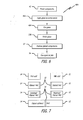
- Fig. 6 is a flow chart illustrating an alternate method 40A for glaze soldering laser components in accordance with the teachings of the present invention
- Fig. 7 is a diagram illustrating this method with butt joint soldering of two core sections.
- the components a doped YAG core 12 and undoped YAG input section 14 are shown in Fig. 7) are polished.
- a layer of glaze 32 is applied to each component on the surfaces to be joined together.
- the two components are then fired to form two components (still separate) each with a glazed surface.
- each glaze layer 32 is polished so that it becomes flat.
- the thickness of the fired glaze layer 32 may be greater than desired, so the glaze layer 32 can be polished to reduce its thickness.
- the two components are positioned together with the two glaze layers in intimate contact. If desired, by applying axial pressure to the soldering units, the thickness of the solder layer can be additionally reduced.
- the sections are fired again to join the components together and complete the soldering process. This method allows for more control over the formed glaze interface.
- An alternate method for glaze soldering involves the use of pre-formed glaze sheets.
- the selected glaze can be pre-fired and machined into strips or sheets of the desired thickness.
- the pre-formed sheets are then mounted between components to be joined and fired again in a secondary firing cycle, thereby soldering the components together.
- the use of these glaze pre-forms may be preferable to ensure a more uniform interface. Glaze pre-forms may also be easier to apply to large area crystals or ceramics.
- the glaze since the glaze has been pre-melted to form cladding strips, re-melting them requires less energy and lower temperatures. In contrast to crystalline raw oxides that melt suddenly, the pre-melted glazes soften over a range of temperatures. The melting temperature of the secondary cycle can therefore be reduced.
- Eutectic glazes are typically powdered mixes of three to four oxides, alkalis, etc.
- the first stage of glazing is a fritting that typically includes a) mixing of the powdered oxides, b) melting, c) quenching in cold water, and d) grinding into a fine powder.
- the raw glaze often does not mix well to form an evenly dispersed multi-oxide powder.
- the fritting employs only mechanical mixing to assure homogeneity of the glaze cladding layer. The dissolution and much localized migration can also affect the homogeneity. With the above re-melting step, even at the lowered fusion temperature, the homogeneity of the re-processed glaze improves its refractivity and reduces its light absorption.
- Eutectic glaze soldering is applicable to all joints existing in composite laser components, such as butt, lap (including scarf, tapered lap, overlap, etc), and various strap joints.
- the glazing may include various deposition techniques: spray deposition, deposition of water-based glaze slurries, and deposition of dry glaze powders. With these solder joints, glaze soldering and deposition techniques, a wide variety of laser component designs can be accomplished.
- the novel glaze soldering techniques can be used to join the main (core) sections of a laser component, as well as to join cladding units or auxiliary units (such as various prisms) to the main sections.
- the sections to be joined may include two laser materials - identical, similar (for instance, doped and undoped, or differently doped same basic materials), or dissimilar oxide crystals and ceramics and various combinations. For instance, a particular interest exists for joining two differently doped YAG crystals, YAG crystals and YAG ceramics, YAG and Sapphire or Spinel crystals, etc. With glaze soldering, lattice and thermal mismatches between dissimilar materials can be compromised.
- glaze soldered crystal and ceramic laser components of the present invention is not limited to the described designs of slabs and rods, but to other devices and shapes, such as composite discs, coated rods of elliptical cross-section, as well as to various fiber-laser components.
Landscapes
- Physics & Mathematics (AREA)
- Electromagnetism (AREA)
- Chemical & Material Sciences (AREA)
- Crystallography & Structural Chemistry (AREA)
- Engineering & Computer Science (AREA)
- Plasma & Fusion (AREA)
- Optics & Photonics (AREA)
- Lasers (AREA)
- Ceramic Products (AREA)
Abstract
Description
- The present invention relates to solid-state laser technology. More specifically, the present invention relates to techniques and materials for joining laser components.
- Recent advances in high-energy diode-pumped solid-state lasers have facilitated extensive developments in the architecture of laser components such as laserable slabs, rods and disks. Solid-state laser slabs typically include a thin planar solid-state gain medium (core plate) that is encapsulated by a solid crystal cladding. The core plate, primarily having a rectangular cross-section, is a key laser component affecting beam quality at high energy levels. Commercial laser slabs are typically comprised of single crystals, such as Yb:YAG (ytterbium doped yttrium-aluminum-garnet) and Nd:YAG (neodymium doped yttrium-aluminum-garnet), or polycrystalline transparent ceramics, such as Y3A15O12. The core plate often includes two undoped input and output sections bonded to a doped central section. The bonded core is then structurally integrated with a peripheral crystal plate cladding made from material (such as Sapphire, Spinel, or related ceramics) having a step-index refractivity interface with the core to suppress parasitic oscillations that deplete energy in the core gain medium. In addition, a laser slab may also include various prisms joined to the input and output sections for inserting pump light and extracting laser energy from the slab.
- These multiple components need to be joined together without introducing any optical defects in the laser slab. Conventionally, laser components are joined using diffusion bonding. Diffusion bonding typically includes placing the joining crystal or ceramic units in intimate contact and applying external pressure and heat, so the units can be bonded together uniformly throughout. The pressure and temperature can be constant or variable, including various programmable cycles. Various pressurization techniques include those using "hot presses", hydrostatic systems, statically indeterminate systems (which develop intrinsic thermal stresses when heated), and the techniques based on van der Vaals force-assisted optical contacting. All these pressurization techniques, as well as precision grinding and polishing, are commonly used in the fabrication of core components.
- Diffusion bonding of laser components, however, meets enormous difficulties, particularly when bonding dissimilar materials such as YAG and Sapphire. The thermal (CTE) mismatch and high temperature processing (about 1200-1700 °C), as well as the high elastic moduli of Sapphire and YAG, result in high interfacial thermal stresses localized at the slab ends. The crystal dissimilarity (hexagonal vs. cubic) and lattice mismatch between Sapphire and YAG substantially complicate the solid phase interaction between the dissimilar crystals. These difficulties lead to imperfect and low strength interface formation with strong propensity to delamination, reduced thermal conductivity at the imperfect interface, and energy leaks. In addition, diffusion bonding requires very high precision polishing of the components to be joined. This is a time-consuming and expensive process.
- Glass soldering is a well-known technique widely used in electronics and micro-optics for sealing of cathode tubes, liquid crystal displays, micro-optic components, hermetic encapsulation of glass and metal electronic packages, etc. Glass soldering typically uses high temperature melting glasses. In spite of the existing popularity of glass soldering, its application for laser components meets substantial limitations, primarily associated with the high temperature processing, which causes a haze appearance in YAG and increases its light absorption and scattering.
- Hence, a need exists in the art for an improved system or method for joining laser components that is more effective and less expensive than conventional approaches.
- The need in the art is addressed by the glaze soldered solid-state laser active medium of the present invention. The novel laser active medium includes a first section of a first material, a second section of a second material, and a layer of ceramic glaze joining the two sections. The first and second materials may be identical, similar, or dissimilar, and may include crystals or ceramics. The glaze is a multi-oxide eutectic ceramic glaze having a refractivity, light absorption, thermal expansion, and fusion temperature that are compatible with the adherent materials. The sections are joined using a novel glaze soldering process that includes the steps of positioning the sections, applying the ceramic glaze between the sections, and firing the glaze to solder the sections together.
-
- Fig. 1 is a perspective view of a conventional laser slab, comprised of a thin core plate having a rectangular cross-section and including a doped central section and two undoped input and output sections.
- Fig. 1b is a side view of the conventional laser slab of Fig. 1a.
- Fig. 2 is a cross-sectional view of a conventional laser slab with plate cladding.
- Fig. 3 is a perspective view of a conventional laser rod having a circular cross-section and including a doped central section and two undoped input and output sections.
- Fig. 4 is a side view of an illustrative glaze soldered laser slab designed in accordance the teachings of the present invention.
- Fig. 5 is a flow chart illustrating an illustrative method for glaze soldering laser components in accordance with the teachings of the present invention.
- Fig. 6 is a flow chart illustrating an alternate method for glaze soldering laser components in accordance with the teachings of the present invention.
- Fig. 7 is a diagram illustrating the method shown in Fig. 6.
- Illustrative embodiments and exemplary applications will now be described with reference to the accompanying drawings to disclose the advantageous teachings of the present invention.
- While the present invention is described herein with reference to illustrative embodiments for particular applications, it should be understood that the invention is not limited thereto. Those having ordinary skill in the art and access to the teachings provided herein will recognize additional modifications, applications, and embodiments within the scope thereof and additional fields in which the present invention would be of significant utility.
- A laser component typically includes a plurality of sections including a doped central core, undoped input and output sections, cladding, and various attached prisms. Figs. 1-3 show a few example laser component configurations.
- Fig. 1a is a perspective view of a
conventional laser slab 10, and Fig. 1b is a side view of theconventional laser slab 10 of Fig. 1a. Thelaser slab 10 is comprised of a thin core plate having a rectangular cross-section and including a dopedcentral section 12, anundoped input section 14, and anundoped output section 16. The core (solid-state gain medium) can be made from single crystals such as Yb:YAG and Nd:YAG, or from similar oxides in the form of nano-crystalline and fully transparent ceramics, or from combinations of crystals and ceramic sections. Diffusion bonding is typically used to bond these sections. - Fig. 2 is a cross-sectional view of a
laser slab 20 with conventional plate cladding. Thelaser slab 20 includes a Yb:YAG/YAG crystalcomposite core plate 10 that is peripherally encapsulated by solid Sapphirecladding plates 22. Thecladding plates 22 are attached to thecore plate 10 using conventional diffusion bonding. - Laser slabs for high-energy applications typically have a rectangular cross-section. The invention, however, is not limited thereto. Other shapes can also be used without departing from the present teachings. For example, Fig. 3 is a perspective view of a
conventional laser rod 10A having a circular cross-section and including a dopedcentral section 12A and two undoped input andoutput sections - As discussed above, diffusion bonding is typically used to join the multiple sections of a laser component. There are, however, many difficulties associated with diffusion bonding. In accordance with the teachings of the present invention, the sections of a laser component are joined together using glaze soldering.
- Fig. 4 is a side view of an illustrative glaze soldered
laser slab 30 designed in accordance the teachings of the present invention. Thelaser slab 30 includes several components: a dopedcentral core 12 fabricated from a solid-state gain medium such as Yb:YAG, anundoped input section 14, anundoped output section 16, andcladding plates 22 fabricated from a cladding material such as Sapphire. In accordance with the teachings of the present invention, these components are joined together using multi-component eutectic oxide ceramic glaze. Thin layers ofglaze 32 are applied between the laser core components and fired to solder the components together. Note that the thickness of the glaze layers 32 in Fig. 4 is exaggerated for illustrative purposes. The thickness of the solder layer should be thin (about wavelength) to reduce the effects of any differences in refractivity between the glaze and the core materials. - Ceramic glazes are commonly available and inexpensive materials used primarily for pottery and electronics applications. They have not previously been considered for use in lasers or optical systems. Glaze manufacturers therefore typically do not list the optical characteristics such as refractivity and light absorption of the glazes. One of ordinary skill in the art, however, can experimentally determine the refractivity of a glaze.
- The selected glaze should have: 1) a desirable refractivity that closely matches the refractivity of the core materials (preferably within 0.03 difference); 2) low light absorption for both pump and signal wavelengths (on the order of about 10-4 cm-1 or better); 3) close thermal (CTE) compatibility with the core materials (within 1 part per million difference); and 4) low to moderate fusion temperatures (certainly less than the bonding temperatures of the core materials). Preferably, the thermal conductivity and diffusivity should be high enough to provide an efficient heat transfer where it is needed. They also can be similar to those parameters in the core materials. This is not necessary, however, since the glaze layer is typically very thin thus the thermal resistance is low. When the optical and thermal parameters of the selected glaze are compatible with the parameters of core materials, then the anticipated reflection, scattering, and acoustic resonance bouncing, as well as thermal excursion and stress-induced birefringence are minimized.
- The eutectic ceramic glazes applicable for soldering of YAG materials are primarily Pb-B-Si-Al and Bi-B-Zn eutectic oxides. Table 1 correlates overall properties of electronic grade commercial glazes (primarily from manufacturers Ferro and NEG) with the properties of Yb:YAG. Their optical, thermal, and mechanical properties provide nearly stress-free interface with a refractivity difference not exceeding 0.03. For example, IP 540 Ferro and EG 2868 Ferro are commercial glazes that almost satisfy all the listed criteria for the soldering application. IP 540 Ferro is an adequate commercial soldering glaze. Its refractivity, n=1.79-1.80, is very close to the refractivity of YAG, n=1.82. The refractivity difference of 0.03 leads to the thickness of the solder layer not exceeding 5 microns. With the IP 540 Ferro glaze, the firing temperature is as low as 550-575°C, and the duration of the firing cycle is only about 1.5-2 hours.
Table 1 Pb-B-Si-Al & Bi-B-Zn Commercial Glazes YAG, Yb-doped crystals Vitreous/polycrystalline ceramics Crystal symmetry: cubic Lattice parameters: n/a Lattice constant: a=12.01A Transparent at 0.18-4.5 microns Transparent at 0.18-4.5 microns Density = 2.8-3 g/cm3 Density = 4.56 g/cm3 Hardness (Mohs): 7.5-8.0 Hardness (Mohs): 8.25-8.5 Thermal conductivity: k=1.5-3 W/m/K (@T=20°C) Thermal conductivity: k=14 W/m/K (@T=20°C) and k=10.5 W/mK (@T=100°C) Fusion point T*= 550-900°C Melting point T*=1970°C CTE =7-9 10-6/K (Over.=8.4) CTE =7.8 10-6/K (al) Refractive index@1.0µm: 1.7-1.82 Refractive index@1.0µm: 1.82 - A variety of methods can be used to apply the glaze to the components. For example, the glaze powder can be mixed with DI (de-ionized) water to form a slurry. The slurry then can be dispensed or sprayed onto the surface of the crystal sections, dried and fired. Other methods for applying glaze can also be used without departing from the scope of the present teachings.
- Fig. 5 is a flow chart illustrating an
illustrative method 40 for glaze soldering laser components in accordance with the teachings of the present invention. First, atStep 42, the components to be joined are machined and polished. The sections can be diced from crystal boules or ceramic pre-forms and polished. Soldering does not require a high level of polishing (as does diffusion bonding) since the glaze will provide an interface between the two components. AtStep 44, the components are placed in the desired position with a gap between the two components and held in place by appropriate mounting fixtures, and atStep 46, the glaze slurry is applied to the gap to form a layer of glaze between the components. AtStep 48, the glaze is fired at a temperature appropriate for the chosen glaze material. As shown in Table 1, eutectic glazes allow processing at relatively low temperatures (about 550-900°C), significantly lower than the melting point of the gain medium (1970°C for YAG) or heat treatment temperatures associated with conventional diffusion bonding (for instance, 1100 - 1700 °C for YAG-to-YAG joints). (Excessive temperatures in crystal fabrication processes (especially those exceeding 80% of the melting point) can induce haze or otherwise damage the core crystal and are therefore undesirable.) If necessary, atStep 50, any excess glaze can be removed through polishing. This process can then be repeated to join additional components. The details of the component mounting, fixture (retaining walls), glaze application, etc. are apparent to those skilled in the art of glaze processing. - Multiple components can be soldered in one firing cycle, or separately. For alignment purposes, it may be desirable to solder each interface separately. For example, the input section can be soldered to the central core during a first firing cycle, and the output section can be soldered to the central core during a subsequent second firing cycle. In this case, multiple glazes can be used for the soldering, each glaze having a different firing temperature. Thus, successive firing cycles can use glazes with lower firing temperatures to prevent previously soldered interfaces from melting.
- Fig. 6 is a flow chart illustrating an
alternate method 40A for glaze soldering laser components in accordance with the teachings of the present invention, and Fig. 7 is a diagram illustrating this method with butt joint soldering of two core sections. AtStep 42, the components (adoped YAG core 12 and undopedYAG input section 14 are shown in Fig. 7) are polished. AtStep 46A, a layer ofglaze 32 is applied to each component on the surfaces to be joined together. AtStep 48A, the two components are then fired to form two components (still separate) each with a glazed surface. AtStep 50A, eachglaze layer 32 is polished so that it becomes flat. In addition, the thickness of the firedglaze layer 32 may be greater than desired, so theglaze layer 32 can be polished to reduce its thickness. AtStep 52, the two components are positioned together with the two glaze layers in intimate contact. If desired, by applying axial pressure to the soldering units, the thickness of the solder layer can be additionally reduced. AtStep 54, in a second firing cycle, the sections are fired again to join the components together and complete the soldering process. This method allows for more control over the formed glaze interface. - An alternate method for glaze soldering involves the use of pre-formed glaze sheets. The selected glaze can be pre-fired and machined into strips or sheets of the desired thickness. The pre-formed sheets are then mounted between components to be joined and fired again in a secondary firing cycle, thereby soldering the components together. The use of these glaze pre-forms may be preferable to ensure a more uniform interface. Glaze pre-forms may also be easier to apply to large area crystals or ceramics. In addition, since the glaze has been pre-melted to form cladding strips, re-melting them requires less energy and lower temperatures. In contrast to crystalline raw oxides that melt suddenly, the pre-melted glazes soften over a range of temperatures. The melting temperature of the secondary cycle can therefore be reduced.
- Eutectic glazes are typically powdered mixes of three to four oxides, alkalis, etc. The first stage of glazing is a fritting that typically includes a) mixing of the powdered oxides, b) melting, c) quenching in cold water, and d) grinding into a fine powder. The raw glaze often does not mix well to form an evenly dispersed multi-oxide powder. The fritting employs only mechanical mixing to assure homogeneity of the glaze cladding layer. The dissolution and much localized migration can also affect the homogeneity. With the above re-melting step, even at the lowered fusion temperature, the homogeneity of the re-processed glaze improves its refractivity and reduces its light absorption.
- In addition, with the suggested glaze pre-forms and the lower temperature re-melting, there may be some reduction in the devitrification of the glaze when cooling, as well as reduction in hairline cracking (dunting) and crazing (if any).
- Among other benefits of the multi-oxide eutectic ceramics is the possibility to optimize commercial glazes and, therefore, their properties, primarily their refractivity and thermal expansion. By understanding why different oxides have certain properties, specialists experienced in the field of ceramics will be able to select the proper commercial glaze and modify its refractivity and linear expansion for a desired slab design and firing cycle.
- Eutectic glaze soldering is applicable to all joints existing in composite laser components, such as butt, lap (including scarf, tapered lap, overlap, etc), and various strap joints. The glazing may include various deposition techniques: spray deposition, deposition of water-based glaze slurries, and deposition of dry glaze powders. With these solder joints, glaze soldering and deposition techniques, a wide variety of laser component designs can be accomplished.
- The novel glaze soldering techniques can be used to join the main (core) sections of a laser component, as well as to join cladding units or auxiliary units (such as various prisms) to the main sections. The sections to be joined may include two laser materials - identical, similar (for instance, doped and undoped, or differently doped same basic materials), or dissimilar oxide crystals and ceramics and various combinations. For instance, a particular interest exists for joining two differently doped YAG crystals, YAG crystals and YAG ceramics, YAG and Sapphire or Spinel crystals, etc. With glaze soldering, lattice and thermal mismatches between dissimilar materials can be compromised.
- Application of the glaze soldered crystal and ceramic laser components of the present invention is not limited to the described designs of slabs and rods, but to other devices and shapes, such as composite discs, coated rods of elliptical cross-section, as well as to various fiber-laser components.
- Thus, the present invention has been described herein with reference to a particular embodiment for a particular application. Those having ordinary skill in the art and access to the present teachings will recognize additional modifications, applications and embodiments within the scope thereof. For example, while the invention has been described with reference to Yb:YAG/YAG composite crystals, the invention is not limited thereto. Various glaze materials, design configurations, and deposition techniques are also considered within the scope of the present invention and can be used for other crystal or ceramic gain media cores. Furthermore, while the invention has been described with reference to solid-state laser components, the glaze soldering technique can be applied to other applications to join crystal and/or ceramic materials without departing from the scope of the present teachings.
- It is therefore intended by the appended claims to cover any and all such applications, modifications and embodiments within the scope of the present invention.
- Accordingly,
Claims (11)
- A solid-state laser active medium (30) characterized by:a first section (12) of a first material;a second section (14) of a second material; anda layer of ceramic glaze (32) joining said first and second sections (12, 14).
- The invention of Claim 1 wherein said glaze is a eutectic glaze.
- The invention of Claim 1 wherein said glaze is a multi-oxide glaze.
- The invention of Claim 1 wherein said glaze has a refractivity that closely matches a refractivity of said first material.
- The invention of Claim 1 wherein said glaze has low light absorption for pump and signal wavelengths of said first material.
- The invention of Claim 1 wherein said glaze has a close thermal compatibility with said first material.
- The invention of Claim 1 wherein said glaze has low to moderate fusion temperatures relative to the bonding temperatures of said first and second materials.
- The invention of Claim 1 wherein said first and second materials are identical or similar.
- The invention of Claim 1 wherein said first and second materials are dissimilar.
- The invention of Claim 1 wherein said first material is crystal or ceramics.
- The invention of Claim 1 wherein said second material is crystal or ceramics.
Applications Claiming Priority (1)
| Application Number | Priority Date | Filing Date | Title |
|---|---|---|---|
| US11/103,894 US7630423B2 (en) | 2005-04-12 | 2005-04-12 | Glaze soldered laser components and method of manufacturing |
Publications (2)
| Publication Number | Publication Date |
|---|---|
| EP1713149A1 true EP1713149A1 (en) | 2006-10-18 |
| EP1713149B1 EP1713149B1 (en) | 2014-09-24 |
Family
ID=36440897
Family Applications (1)
| Application Number | Title | Priority Date | Filing Date |
|---|---|---|---|
| EP06251719.8A Ceased EP1713149B1 (en) | 2005-04-12 | 2006-03-29 | Glaze soldered laser components and method of manufacturing |
Country Status (2)
| Country | Link |
|---|---|
| US (1) | US7630423B2 (en) |
| EP (1) | EP1713149B1 (en) |
Cited By (2)
| Publication number | Priority date | Publication date | Assignee | Title |
|---|---|---|---|---|
| WO2006130180A3 (en) * | 2004-12-23 | 2007-02-22 | Raytheon Co | Glaze cladding for laser components and method of encapsulation |
| WO2007120432A3 (en) * | 2006-04-14 | 2008-03-13 | Raytheon Co | Solid-state laser with spatially-tailored active ion concentration using valence conversion with surface masking and method |
Families Citing this family (8)
| Publication number | Priority date | Publication date | Assignee | Title |
|---|---|---|---|---|
| US9601647B2 (en) * | 2013-07-18 | 2017-03-21 | The Chinese University Of Hong Kong | Converting infrared light into broadband visible light at high efficiency using lanthanide-sensitized oxides |
| GB201500304D0 (en) | 2015-01-09 | 2015-02-25 | Rolls Royce Plc | A method of surface-treating a cast intermetallic component |
| US9601904B1 (en) | 2015-12-07 | 2017-03-21 | Raytheon Company | Laser diode driver with variable input voltage and variable diode string voltage |
| US20180093917A1 (en) * | 2016-10-03 | 2018-04-05 | Raytheon Company | Molding composite and method of making molded part |
| CN107453191A (en) * | 2017-07-18 | 2017-12-08 | 中国电子科技集团公司第十研究所 | A kind of lath gain media and its manufacture method with radiator structure |
| CN107394571B (en) * | 2017-08-07 | 2019-07-16 | 中国电子科技集团公司第十一研究所 | A kind of packaging method of slab laser crystal and slab laser crystal |
| EP3787133B1 (en) * | 2018-04-25 | 2024-10-23 | National Institute for Materials Science | Bonded body, laser oscillator, laser amplifier, and method for producing bonded body |
| WO2021157135A1 (en) * | 2020-02-07 | 2021-08-12 | Jx金属株式会社 | Yag ceramic joined body and production method therefor |
Citations (6)
| Publication number | Priority date | Publication date | Assignee | Title |
|---|---|---|---|---|
| GB1454496A (en) * | 1972-11-30 | 1976-11-03 | Ferranti Ltd | Glazes for ceramic articles |
| US4507787A (en) * | 1982-09-28 | 1985-03-26 | Quantronix Corporation | Segmented YAG laser rods and methods of manufacture |
| EP0820129A1 (en) * | 1996-02-02 | 1998-01-21 | Fanuc Ltd | Solid laser oscillator |
| EP0854551A2 (en) * | 1997-01-14 | 1998-07-22 | Trw Inc. | Three-level laser system |
| US5846638A (en) * | 1988-08-30 | 1998-12-08 | Onyx Optics, Inc. | Composite optical and electro-optical devices |
| US6025060A (en) * | 1988-08-30 | 2000-02-15 | Onyx Optics, Inc. | Method and apparatus for composite gemstones |
Family Cites Families (12)
| Publication number | Priority date | Publication date | Assignee | Title |
|---|---|---|---|---|
| US3993844A (en) * | 1974-12-30 | 1976-11-23 | Gte Sylvania Incorporated | Composite ceramic articles and method of making |
| US4018374A (en) | 1976-06-01 | 1977-04-19 | Ford Aerospace & Communications Corporation | Method for forming a bond between sapphire and glass |
| US4350532A (en) * | 1980-09-08 | 1982-09-21 | Minnesota Mining And Manufacturing Company | Glass composition and articles |
| US4772511A (en) * | 1985-11-22 | 1988-09-20 | Minnesota Mining And Manufacturing Company | Transparent non-vitreous zirconia microspheres |
| US5852622A (en) | 1988-08-30 | 1998-12-22 | Onyx Optics, Inc. | Solid state lasers with composite crystal or glass components |
| US5394420A (en) * | 1994-01-27 | 1995-02-28 | Trw Inc. | Multiform crystal and apparatus for fabrication |
| US5974061A (en) | 1997-12-19 | 1999-10-26 | Raytheon Company | Laser pump cavity apparatus with improved thermal lensing control, cooling, and fracture strength and method |
| JP4836102B2 (en) | 2000-06-30 | 2011-12-14 | Hoya株式会社 | Optical element positioning member, optical element positioning member manufacturing method, optical unit, optical unit manufacturing method, lens chip, and floating head for optical memory medium |
| US6587488B1 (en) | 2000-11-08 | 2003-07-01 | Maxios Laser Corporation | Control of parasitic laser oscillations in solid-state lasers by frustrating total internal reflections |
| AU2002222688A1 (en) * | 2000-12-20 | 2002-07-01 | Murata Manufacturing Co., Ltd. | Transparent ceramic and method for production thereof, and optical element |
| JP2003258350A (en) * | 2002-02-27 | 2003-09-12 | Nec Corp | Composite laser rod, method of manufacturing the same, and laser device using the same |
| US7675952B2 (en) * | 2004-12-23 | 2010-03-09 | Raytheon Company | Articulated glaze cladding for laser components and method of encapsulation |
-
2005
- 2005-04-12 US US11/103,894 patent/US7630423B2/en not_active Expired - Lifetime
-
2006
- 2006-03-29 EP EP06251719.8A patent/EP1713149B1/en not_active Ceased
Patent Citations (6)
| Publication number | Priority date | Publication date | Assignee | Title |
|---|---|---|---|---|
| GB1454496A (en) * | 1972-11-30 | 1976-11-03 | Ferranti Ltd | Glazes for ceramic articles |
| US4507787A (en) * | 1982-09-28 | 1985-03-26 | Quantronix Corporation | Segmented YAG laser rods and methods of manufacture |
| US5846638A (en) * | 1988-08-30 | 1998-12-08 | Onyx Optics, Inc. | Composite optical and electro-optical devices |
| US6025060A (en) * | 1988-08-30 | 2000-02-15 | Onyx Optics, Inc. | Method and apparatus for composite gemstones |
| EP0820129A1 (en) * | 1996-02-02 | 1998-01-21 | Fanuc Ltd | Solid laser oscillator |
| EP0854551A2 (en) * | 1997-01-14 | 1998-07-22 | Trw Inc. | Three-level laser system |
Cited By (4)
| Publication number | Priority date | Publication date | Assignee | Title |
|---|---|---|---|---|
| WO2006130180A3 (en) * | 2004-12-23 | 2007-02-22 | Raytheon Co | Glaze cladding for laser components and method of encapsulation |
| US7675952B2 (en) | 2004-12-23 | 2010-03-09 | Raytheon Company | Articulated glaze cladding for laser components and method of encapsulation |
| WO2007120432A3 (en) * | 2006-04-14 | 2008-03-13 | Raytheon Co | Solid-state laser with spatially-tailored active ion concentration using valence conversion with surface masking and method |
| US7995631B2 (en) | 2006-04-14 | 2011-08-09 | Raytheon Company | Solid-state laser with spatially-tailored active ion concentration using valence conversion with surface masking and method |
Also Published As
| Publication number | Publication date |
|---|---|
| US20060227829A1 (en) | 2006-10-12 |
| EP1713149B1 (en) | 2014-09-24 |
| US7630423B2 (en) | 2009-12-08 |
Similar Documents
| Publication | Publication Date | Title |
|---|---|---|
| US5852622A (en) | Solid state lasers with composite crystal or glass components | |
| US5563899A (en) | Composite solid state lasers of improved efficiency and beam quality | |
| US5846638A (en) | Composite optical and electro-optical devices | |
| EP1713149B1 (en) | Glaze soldered laser components and method of manufacturing | |
| EP1834387B1 (en) | Glaze cladding for laser components | |
| WO2005112208A1 (en) | Composite laser element and laser oscillator employing it | |
| US9478936B2 (en) | Laser crystal components joined with thermal management devices | |
| US11349274B2 (en) | Amplifier assembly | |
| JP3223183B2 (en) | Method of manufacturing holding device for semiconductor disk and holding device manufactured by the method | |
| KR20240100353A (en) | Manufacturing method of composite optical ceramic device | |
| US6895152B2 (en) | Guided-mode laser apparatus with improved cladding structure and a method of fabricating thereof | |
| JPH02153849A (en) | Composite consisting of glass-containing substance and glass-free substance, and method for forming said composite | |
| EP1737802B1 (en) | Silicon carbide bonding | |
| CN107749559A (en) | A kind of pump coupling device and its manufacture method | |
| CN109193334A (en) | The preparation method of disc waveguide laser crystal | |
| CN109149350A (en) | A kind of double clad disc waveguide laser crystal | |
| RU2560438C1 (en) | Method of parts connection of optical element out of garnet crystals | |
| CN109149349A (en) | A kind of disc waveguide laser crystal of three-decker | |
| TW202116691A (en) | Manufacturing method of heat reflecting member and glass member with heat reflecting layer | |
| US12160081B2 (en) | YAG ceramic joined body and production method therefor | |
| RU2749153C1 (en) | Method for creation of composite laser element based on oxide crystals | |
| CN120329067A (en) | A diffusion bonding method for transparent aluminum oxynitride ceramics | |
| Ikesue et al. | Other Important Technologies | |
| CN109309339A (en) | Disc waveguide laser crystal | |
| Jedamzik et al. | Closed back lightweight ZERODUR mirrors with adhesive-free fusing |
Legal Events
| Date | Code | Title | Description |
|---|---|---|---|
| PUAI | Public reference made under article 153(3) epc to a published international application that has entered the european phase |
Free format text: ORIGINAL CODE: 0009012 |
|
| AK | Designated contracting states |
Kind code of ref document: A1 Designated state(s): AT BE BG CH CY CZ DE DK EE ES FI FR GB GR HU IE IS IT LI LT LU LV MC NL PL PT RO SE SI SK TR |
|
| AX | Request for extension of the european patent |
Extension state: AL BA HR MK YU |
|
| 17P | Request for examination filed |
Effective date: 20070330 |
|
| AKX | Designation fees paid |
Designated state(s): DE FR GB |
|
| 17Q | First examination report despatched |
Effective date: 20071109 |
|
| RIC1 | Information provided on ipc code assigned before grant |
Ipc: H01S 3/16 20060101ALN20140122BHEP Ipc: H01S 3/06 20060101AFI20140122BHEP |
|
| RIC1 | Information provided on ipc code assigned before grant |
Ipc: H01S 3/06 20060101AFI20140127BHEP Ipc: H01S 3/16 20060101ALN20140127BHEP |
|
| GRAP | Despatch of communication of intention to grant a patent |
Free format text: ORIGINAL CODE: EPIDOSNIGR1 |
|
| RIC1 | Information provided on ipc code assigned before grant |
Ipc: H01S 3/16 20060101ALN20140314BHEP Ipc: H01S 3/06 20060101AFI20140314BHEP |
|
| INTG | Intention to grant announced |
Effective date: 20140410 |
|
| GRAS | Grant fee paid |
Free format text: ORIGINAL CODE: EPIDOSNIGR3 |
|
| GRAA | (expected) grant |
Free format text: ORIGINAL CODE: 0009210 |
|
| AK | Designated contracting states |
Kind code of ref document: B1 Designated state(s): DE FR GB |
|
| REG | Reference to a national code |
Ref country code: GB Ref legal event code: FG4D |
|
| REG | Reference to a national code |
Ref country code: DE Ref legal event code: R096 Ref document number: 602006043123 Country of ref document: DE Effective date: 20141106 |
|
| REG | Reference to a national code |
Ref country code: DE Ref legal event code: R097 Ref document number: 602006043123 Country of ref document: DE |
|
| PLBE | No opposition filed within time limit |
Free format text: ORIGINAL CODE: 0009261 |
|
| STAA | Information on the status of an ep patent application or granted ep patent |
Free format text: STATUS: NO OPPOSITION FILED WITHIN TIME LIMIT |
|
| 26N | No opposition filed |
Effective date: 20150625 |
|
| REG | Reference to a national code |
Ref country code: FR Ref legal event code: PLFP Year of fee payment: 11 |
|
| REG | Reference to a national code |
Ref country code: FR Ref legal event code: PLFP Year of fee payment: 12 |
|
| REG | Reference to a national code |
Ref country code: FR Ref legal event code: PLFP Year of fee payment: 13 |
|
| PGFP | Annual fee paid to national office [announced via postgrant information from national office to epo] |
Ref country code: FR Payment date: 20230222 Year of fee payment: 18 |
|
| PGFP | Annual fee paid to national office [announced via postgrant information from national office to epo] |
Ref country code: GB Payment date: 20230221 Year of fee payment: 18 Ref country code: DE Payment date: 20230221 Year of fee payment: 18 |
|
| P01 | Opt-out of the competence of the unified patent court (upc) registered |
Effective date: 20230530 |
|
| REG | Reference to a national code |
Ref country code: DE Ref legal event code: R119 Ref document number: 602006043123 Country of ref document: DE |
|
| GBPC | Gb: european patent ceased through non-payment of renewal fee |
Effective date: 20240329 |
|
| PG25 | Lapsed in a contracting state [announced via postgrant information from national office to epo] |
Ref country code: DE Free format text: LAPSE BECAUSE OF NON-PAYMENT OF DUE FEES Effective date: 20241001 |
|
| PG25 | Lapsed in a contracting state [announced via postgrant information from national office to epo] |
Ref country code: GB Free format text: LAPSE BECAUSE OF NON-PAYMENT OF DUE FEES Effective date: 20240329 |
|
| PG25 | Lapsed in a contracting state [announced via postgrant information from national office to epo] |
Ref country code: FR Free format text: LAPSE BECAUSE OF NON-PAYMENT OF DUE FEES Effective date: 20240331 |
|
| PG25 | Lapsed in a contracting state [announced via postgrant information from national office to epo] |
Ref country code: GB Free format text: LAPSE BECAUSE OF NON-PAYMENT OF DUE FEES Effective date: 20240329 Ref country code: FR Free format text: LAPSE BECAUSE OF NON-PAYMENT OF DUE FEES Effective date: 20240331 Ref country code: DE Free format text: LAPSE BECAUSE OF NON-PAYMENT OF DUE FEES Effective date: 20241001 |