EP1710914A1 - Input protection circuit - Google Patents
Input protection circuit Download PDFInfo
- Publication number
- EP1710914A1 EP1710914A1 EP05254322A EP05254322A EP1710914A1 EP 1710914 A1 EP1710914 A1 EP 1710914A1 EP 05254322 A EP05254322 A EP 05254322A EP 05254322 A EP05254322 A EP 05254322A EP 1710914 A1 EP1710914 A1 EP 1710914A1
- Authority
- EP
- European Patent Office
- Prior art keywords
- input
- pull
- output terminal
- external input
- input protection
- Prior art date
- Legal status (The legal status is an assumption and is not a legal conclusion. Google has not performed a legal analysis and makes no representation as to the accuracy of the status listed.)
- Withdrawn
Links
Images





Classifications
-
- H—ELECTRICITY
- H02—GENERATION; CONVERSION OR DISTRIBUTION OF ELECTRIC POWER
- H02H—EMERGENCY PROTECTIVE CIRCUIT ARRANGEMENTS
- H02H7/00—Emergency protective circuit arrangements specially adapted for specific types of electric machines or apparatus or for sectionalised protection of cable or line systems, and effecting automatic switching in the event of an undesired change from normal working conditions
- H02H7/20—Emergency protective circuit arrangements specially adapted for specific types of electric machines or apparatus or for sectionalised protection of cable or line systems, and effecting automatic switching in the event of an undesired change from normal working conditions for electronic equipment
-
- H—ELECTRICITY
- H10—SEMICONDUCTOR DEVICES; ELECTRIC SOLID-STATE DEVICES NOT OTHERWISE PROVIDED FOR
- H10D—INORGANIC ELECTRIC SEMICONDUCTOR DEVICES
- H10D89/00—Aspects of integrated devices not covered by groups H10D84/00 - H10D88/00
- H10D89/60—Integrated devices comprising arrangements for electrical or thermal protection, e.g. protection circuits against electrostatic discharge [ESD]
- H10D89/601—Integrated devices comprising arrangements for electrical or thermal protection, e.g. protection circuits against electrostatic discharge [ESD] for devices having insulated gate electrodes, e.g. for IGFETs or IGBTs
-
- H—ELECTRICITY
- H03—ELECTRONIC CIRCUITRY
- H03K—PULSE TECHNIQUE
- H03K19/00—Logic circuits, i.e. having at least two inputs acting on one output; Inverting circuits
- H03K19/003—Modifications for increasing the reliability for protection
- H03K19/00315—Modifications for increasing the reliability for protection in field-effect transistor circuits
Definitions
- the present invention relates to an input protection circuit, and more specifically to an input protection circuit capable of controlling the validity/invalidity of pull-up/pull-down.
- an input protection resistor is input between an internal circuit such as an integrated circuit, etc. and an external input terminal (input pad) to protect the internal circuit (internal transistor, etc.) against static electricity.
- an external input terminal enters an open state
- pull-up resistor/pull-down resistor is inserted to keep a high level state/low level state, and protect an internal circuit from a malfunction due to the influence of noise, etc.
- Japanese Published Patent Application No. Hei 03-079120 discloses an input protection circuit (Figs. 3 and 4 of Japanese Published Patent Application No. Hei 03-079120 ) having an input protection resistor inserted between an external input terminal and an internal circuit, and a pull-up or pull-down resistor one terminal of which is connected to a predetermined power source and the other terminal is connected between the input protection resistor and the internal circuit, and an input protection circuit (Figs. 1 and 2 of Japanese Published Patent Application No. Hei 03-079120 ) having an input protection resistor inserted between an external input terminal and an internal circuit, and a pull-up or pull-down resistor one terminal of which is connected to a predetermined power source and the other terminal is connected between the external input terminal and the input protection resistor.
- the above-mentioned pull-up resistor/pull-down resistor is used in various types of usage, and can be requested to have the function of nullifying the pull-up/pull-down as necessary.
- a leakage test is performed for quality assurance. For example, when it is checked whether or not there occurs a physical short circuit between the external input terminals of a data bus, it is necessary to nullify the pull-up/pull-down provided for the input unit of the internal circuit, apply a voltage between external input terminals, and measure the leakage current.
- Fig. 1 shows a circuit in which a pull-up resistor Rpu is configured by a p-type MOS transistor 70, one terminal is connected to a power source Vdd and the other terminal is connected between an input protection resistor 71 and a buffer circuit (internal circuit) 72.
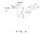
- Fig. 4 shows a circuit in which a pull-up resistor Rpd is configured by an n-type MOS transistor 74, one terminal is connected to a power source Vss and the other terminal is connected between an input protection resistor 71 and a buffer circuit 72.
- V pad V th ⁇ V shift_pu
- Fig. 2 shows the relationship between the input voltage Vin and the output voltage Vout of the buffer circuit 72 shown in Fig. 1 when the MOS transistor 70 enters an OFF state.
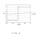
- Fig. 3 shows the relationship between the input voltage Vin and the output voltage Vout of the buffer circuit 72 shown in Fig. 1 when the MOS transistor 70 enters the ON state.
- V shift_pd ( V pad ⁇ V s s ) ⁇ R e s d / ( R p d + R e s d )
- V in V pad ⁇ V shift_pd
- V pad V th + V shift_pd
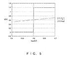
- Fig. 5 shows the relationship between the input voltage Vin and the output voltage Vout of the buffer circuit 72 shown in Fig. 4 when the MOS transistor 74 enters an OFF state.
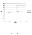
- Fig. 6 shows the relationship between the input voltage Vin and the output voltage Vout of the buffer circuit 72 shown in Fig. 4 when the MOS transistor 74 enters the ON state.
- the threshold voltage viewed from the external input terminal 73 fluctuates, it causes the problem of degradation in characteristic to the input signal that the duty ratio of an input clock signal also fluctuates.
- the present invention has been developed to solve the above-mentioned problems, and aims at providing an input protection circuit capable of controlling the validity/invalidity of the pull-up/pull-down without degradation in characteristic.
- the input protection circuit includes: a first input protection unit which is connected between an external input/output terminal and an internal circuit, and protects the internal circuit against an overvoltage input to the external input/output terminal; and a pull-up unit which is connected between a predetermined voltage source and a point between the external input/output terminal and the first input protection unit., holds a predetermined voltage when the external input/output terminal opens, and has a switch unit for switching validity/invalidity of the pull-up unit.
- the pull-up unit can switch the validity/invalidity of the pull-up unit using a switch unit. Therefore, for example, the pull-up unit can be switched between validity and invalidity as necessary at a leakage test, etc.
- the pull-up unit is connected between a predetermined voltage source and a point between the external input terminal and the first input protection unit, the degradation in characteristic that the threshold voltage of the buffer circuit connected to the internal circuit depends on the validity/invalidity of the pull-up unit (shift) can be prevented.
- the input protection circuit has a similar effect by including: a first input protection unit which is connected between an external input/output terminal and an internal circuit, and protects the internal circuit against an overvoltage input to the external input/output terminal; and a pull-down unit which is connected between a predetermined voltage source and a point between the external input/output terminal and the first input protection unit, holds a predetermined voltage when the external input/output terminal opens, and has a switch unit for switching validity/invalidity of the pull-down unit.
- the present invention can provide an input protection circuit capable of controlling the validity/invalidity of pull-up/pull-down without degradation in characteristic.
- Figs. 7 and 8 show examples of the configurations of the input protection circuit according to the embodiments of the present invention.
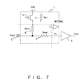
- Fig. 7 shows an example of the configuration of the input protection circuit capable of controlling the validity/invalidity of pull-up according to the present invention.
- An input protection circuit 1 according to the present embodiment shown in Fig. 7 comprises: an input protection resistor 4 (first input protection unit) connected between an external input terminal (input pad) 2 and a buffer circuit 3 connected to an internal circuit; and a pull-up unit comprising a p-type MOS transistor (switch unit) 5 one terminal of which is connected to a power source Vdd and the other terminal is connected between the external input terminal 2 and the input protection resistor 4 and an input protection resistor (second input protection unit) 6.
- the MOS transistor 5 is connected in series with the input protection resistor 6.
- the input protection resistor 4 protects an internal transistor connected after the buffer circuit 3 against the overvoltage of the discharge, etc. of static electricity.
- the input protection resistor 6 connected in series with the MOS transistor 5 protects the MOS transistor 5 against the overvoltage of the discharge, etc. of static electricity.
- the internal circuit (MOS transistor 5, and internal transistors connected after the buffer circuit 3) can be protected against the degradation or destruction by the stress of the discharge of static electricity.
- the MOS transistor 5 controls such that the resistor between the source and the drain functions as a pull-up resistor in the ON state, and the pull-up can be nullifies in the OFF state.
- one terminal of the MOS transistor 5 connected in series with the input protection resistor 6 is connected between the external input terminal 2 and the input protection resistor 4, no direct current flows through the input protection resistor 4 from the power source although the pull-up is effective, thereby having the effect of suppressing a DC path in which a threshold voltage shifts.
- Fig. 9 shows the relationship between the input voltage and the output voltage of the buffer circuit 3 shown in Fig. 7 when the MOS transistor 5 enters the OFF state.
- Fig. 10 shows the relationship between the input voltage and the output voltage of the buffer circuit 3 shown in Fig. 7 when the MOS transistor 5 enters the ON state.
- the threshold voltage viewed from the external input terminal 2 shown in Fig. 9 and the threshold voltage shown in Fig. 10 are 0.6 V, and there occurs no shift in threshold voltage.
- Fig. 8 shows an example of the configuration of an input protection circuit capable of controlling the validity/invalidity of pull-down according to the present embodiment.
- An input protection circuit 10 according to the present embodiment shown in Fig. 8 comprises: an input protection resistor 11 (first input protection unit) connected between an external input terminal (input pad) 2 and a buffer circuit 3 connected to an internal circuit; and a pull-down unit comprising an n-type MOS transistor (switch unit) 12 one terminal of which is connected to the ground (Vss) and the other terminal is connected between the external input terminal 2 and the input protection resistor 11 and an input protection resistor (second input protection unit) 13.
- the MOS transistor 12 is connected in series with the input protection resistor 13.
- the input protection resistor 11 protects the internal transistor connected after the buffer circuit 3 against the overvoltage of the discharge, etc. of static electricity
- the input protection resistor 13 protects the MOS transistor 12 against the overvoltage of the discharge, etc. of static electricity.
- the internal circuit (MOS transistor 12, and internal transistors connected after the buffer circuit 3) can be protected against the degradation or destruction by the stress of the discharge of static electricity.
- the MOS transistor 12 controls such that the resistor between the source and the drain functions as a pull-down resistor in the ON state, and the pull-down can be nullifies in the OFF state.
- one terminal of the MOS transistor 12 connected in series with the input protection resistor 13 is connected between the external input terminal 2 and the input protection resistor 11 and, although the pull-up is effective, thereby having the effect of suppressing a DC path in which a threshold voltage shifts.
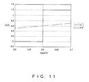
- Fig. 11 shows the relationship between the input voltage and the output voltage of the buffer circuit 3 shown in Fig. 8 when the MOS transistor 12 enters the OFF state.
- Fig. 12 shows the relationship between the input voltage and the output voltage of the buffer circuit 3 shown in Fig. 8 when the MOS transistor 12 enters the ON state.
- the threshold voltage viewed from the external input terminal 2 shown in Fig. 11 and the threshold voltage shown in Fig. 12 are 0.6 V, and there occurs no shift in threshold voltage.
- the MOS transistors 5 and 12 are included in an internal circuit (internal transistor), but the present invention is not limited to these applications, and it is not always necessary to include the MOS transistors 5 and 12 in an internal circuit to obtain the effect of the present invention.
- Figs. 7 and 8 show the case in which the input protection circuit 1 or 10 is used for the external input terminal 2, but the present invention is not limited to this application. That is, when the input protection circuit 1 or 10 according to the present embodiment is used for an external input terminal with the similar effect.
Landscapes
- Engineering & Computer Science (AREA)
- Physics & Mathematics (AREA)
- Computer Hardware Design (AREA)
- Computing Systems (AREA)
- General Engineering & Computer Science (AREA)
- Mathematical Physics (AREA)
- Power Engineering (AREA)
- Semiconductor Integrated Circuits (AREA)
- Logic Circuits (AREA)
Abstract
To provide an input protection circuit capable of controlling the validity/invalidity of pull-up/pull-down without degradation in characteristic, the input protection circuit includes an input protection resistor (4) connected between an external input terminal (2) and a buffer circuit (3) connected to an internal circuit, a p-type MOS transistor (5) one terminal of which is connected to a power source and the other to a point between the external input terminal (2) and the input protection resistor (4), and an input protection resistor (6).
Description
- The present invention relates to an input protection circuit, and more specifically to an input protection circuit capable of controlling the validity/invalidity of pull-up/pull-down.
- Generally, an input protection resistor is input between an internal circuit such as an integrated circuit, etc. and an external input terminal (input pad) to protect the internal circuit (internal transistor, etc.) against static electricity. When an external input terminal enters an open state, pull-up resistor/pull-down resistor is inserted to keep a high level state/low level state, and protect an internal circuit from a malfunction due to the influence of noise, etc.
-
Japanese Published Patent Application No. Hei 03-079120 Japanese Published Patent Application No. Hei 03-079120 Japanese Published Patent Application No. Hei 03-079120 - The above-mentioned pull-up resistor/pull-down resistor is used in various types of usage, and can be requested to have the function of nullifying the pull-up/pull-down as necessary.
- For example, assume that a leakage test is performed for quality assurance. For example, when it is checked whether or not there occurs a physical short circuit between the external input terminals of a data bus, it is necessary to nullify the pull-up/pull-down provided for the input unit of the internal circuit, apply a voltage between external input terminals, and measure the leakage current.
- In this case, for example, the circuit shown in Figs. 1 and 4 can be assumed.
- Fig. 1 shows a circuit in which a pull-up resistor Rpu is configured by a p-
type MOS transistor 70, one terminal is connected to a power source Vdd and the other terminal is connected between aninput protection resistor 71 and a buffer circuit (internal circuit) 72. Similarly, Fig. 4 shows a circuit in which a pull-up resistor Rpd is configured by an n-type MOS transistor 74, one terminal is connected to a power source Vss and the other terminal is connected between aninput protection resistor 71 and abuffer circuit 72. - In Fig. 1, when the
MOS transistor 70 enters an ON state, the input impedance of thebuffer circuit 72 is high. Therefore, a direct current flows from the power source Vdd to an external input terminal (input pad) 73. At this time, the following equation holds where the resistor between the source and drain is represented by Rpu, the resistance value of theinput protection resistor 71 is represented by Resd, the voltage generated by theinput protection resistor 71 is represented by Vshift_pu, the voltage of theexternal input terminal 73 is represented by Vpad, and the input voltage to thebuffer circuit 72 is represented by Vin when theMOS transistor 70 enters the ON state.

- Therefore, when the threshold voltage viewed from the
external input terminal 73 is shifted by the voltage Vshift_pu generated by theinput protection resistor 71, and the threshold voltage of thebuffer circuit 72 is represented by Vth, the following equation holds.
- Fig. 2 shows the relationship between the input voltage Vin and the output voltage Vout of the
buffer circuit 72 shown in Fig. 1 when theMOS transistor 70 enters an OFF state. Fig. 3 shows the relationship between the input voltage Vin and the output voltage Vout of thebuffer circuit 72 shown in Fig. 1 when theMOS transistor 70 enters the ON state. - In Fig. 2, while the threshold voltage viewed from the
external input terminal 73 is about 0.6 V, the threshold voltage shown in Fig. 3 is shifted by about 0.01 V (Vshift_pu). - Likewise, in Fig. 4, when the
MOS transistor 74 enters the ON state, the following equation holds where the resistance between the drain and source is represented by Rpd, and the voltage generated by theinput protection resistor 71 is represented by Vshift_pd.

- Therefore, when the threshold voltage viewed from the
external input terminal 73 is shifted by the voltage Vshift_pd generated by theinput protection resistor 71, and the threshold voltage of thebuffer circuit 72 is represented by Vth, the following equation holds.
- Fig. 5 shows the relationship between the input voltage Vin and the output voltage Vout of the
buffer circuit 72 shown in Fig. 4 when theMOS transistor 74 enters an OFF state. Fig. 6 shows the relationship between the input voltage Vin and the output voltage Vout of thebuffer circuit 72 shown in Fig. 4 when theMOS transistor 74 enters the ON state. - In Fig. 5, while the threshold voltage viewed from the
external input terminal 73 is about 0.6 V, the threshold voltage shown in Fig. 6 is shifted by about 0.01 V (Vshift_pu). - As described above, when the threshold voltage viewed from the
external input terminal 73 fluctuates, it causes the problem of degradation in characteristic to the input signal that the duty ratio of an input clock signal also fluctuates. - Furthermore, it is also possible to use a MOS transistor as the pull-up resistor/pull-down resistor between the external input terminal and the input protection resistor of the input protection circuit disclosed in
Japanese Published Patent Application No. Hei 03-079120 - The present invention has been developed to solve the above-mentioned problems, and aims at providing an input protection circuit capable of controlling the validity/invalidity of the pull-up/pull-down without degradation in characteristic.
- To solve the above-mentioned problems, the input protection circuit according to the present invention includes: a first input protection unit which is connected between an external input/output terminal and an internal circuit, and protects the internal circuit against an overvoltage input to the external input/output terminal; and a pull-up unit which is connected between a predetermined voltage source and a point between the external input/output terminal and the first input protection unit., holds a predetermined voltage when the external input/output terminal opens, and has a switch unit for switching validity/invalidity of the pull-up unit.
- According to the present invention, the pull-up unit can switch the validity/invalidity of the pull-up unit using a switch unit. Therefore, for example, the pull-up unit can be switched between validity and invalidity as necessary at a leakage test, etc.
- Furthermore, since the pull-up unit is connected between a predetermined voltage source and a point between the external input terminal and the first input protection unit, the degradation in characteristic that the threshold voltage of the buffer circuit connected to the internal circuit depends on the validity/invalidity of the pull-up unit (shift) can be prevented.
- Additionally, the input protection circuit according to the present invention has a similar effect by including: a first input protection unit which is connected between an external input/output terminal and an internal circuit, and protects the internal circuit against an overvoltage input to the external input/output terminal; and a pull-down unit which is connected between a predetermined voltage source and a point between the external input/output terminal and the first input protection unit, holds a predetermined voltage when the external input/output terminal opens, and has a switch unit for switching validity/invalidity of the pull-down unit.
- As described above, the present invention can provide an input protection circuit capable of controlling the validity/invalidity of pull-up/pull-down without degradation in characteristic.
-
- Fig. 1 shows an example of a circuit in which a pull-up resistor is configured by a p-type MOS transistor, one terminal is connected to a power source and the other terminal is connected between an input protection resistor and an internal circuit;
- Fig. 2 shows the relationship between an input voltage and an output voltage of a buffer circuit shown in Fig. 1 when a MOS transistor enters an OFF state;
- Fig. 3 shows the relationship between an input voltage and an output voltage of a buffer circuit shown in Fig. 1 when a MOS transistor enters an ON state;
- Fig. 4 shows an example of a circuit in which a pull-down resistor is configured by an n-type MOS transistor, one terminal is connected to a power source and the other terminal is connected between an input protection resistor and an internal circuit;
- Fig. 5 shows the relationship between an input voltage and an output voltage of a buffer circuit shown in Fig. 4 when a MOS transistor enters an OFF state;
- Fig. 6 shows the relationship between an input voltage and an output voltage of a buffer circuit shown in Fig. 4 when a MOS transistor enters an ON state;
- Fig. 7 shows an example of the configuration of an input protection circuit capable of controlling the validity/invalidity of pull-up according to the present embodiment;
- Fig. 8 shows an example of the configuration of an input protection circuit capable of controlling the validity/invalidity of pull-down according to the present embodiment;
- Fig. 9 shows the relationship between an input voltage and an output voltage of a circuit shown in Fig. 7 when a MOS transistor enters an OFF state;
- Fig. 10 shows the relationship between an input voltage and an output voltage of a circuit shown in Fig. 7 when a MOS transistor enters an ON state;
- Fig. 11 shows the relationship between an input voltage and an output voltage of a circuit shown in Fig. 8 when a MOS transistor enters an OFF state; and
- Fig. 12 shows the relationship between an input voltage and an output voltage of a circuit shown in Fig. 8 when a MOS transistor enters an ON state.
- The embodiment of the present invention is explained below by referring to Figs. 7 through 12.
- Figs. 7 and 8 show examples of the configurations of the input protection circuit according to the embodiments of the present invention.
- Fig. 7 shows an example of the configuration of the input protection circuit capable of controlling the validity/invalidity of pull-up according to the present invention.
- An
input protection circuit 1 according to the present embodiment shown in Fig. 7 comprises: an input protection resistor 4 (first input protection unit) connected between an external input terminal (input pad) 2 and abuffer circuit 3 connected to an internal circuit; and a pull-up unit comprising a p-type MOS transistor (switch unit) 5 one terminal of which is connected to a power source Vdd and the other terminal is connected between theexternal input terminal 2 and the input protection resistor 4 and an input protection resistor (second input protection unit) 6. - The
MOS transistor 5 is connected in series with theinput protection resistor 6. - With the above-mentioned configuration, the input protection resistor 4 protects an internal transistor connected after the
buffer circuit 3 against the overvoltage of the discharge, etc. of static electricity. Theinput protection resistor 6 connected in series with theMOS transistor 5 protects theMOS transistor 5 against the overvoltage of the discharge, etc. of static electricity. - Therefore, the internal circuit (
MOS transistor 5, and internal transistors connected after the buffer circuit 3) can be protected against the degradation or destruction by the stress of the discharge of static electricity. - The
MOS transistor 5 controls such that the resistor between the source and the drain functions as a pull-up resistor in the ON state, and the pull-up can be nullifies in the OFF state. - Therefore, for example, it is possible to control the validity/invalidity of pull-up as necessary during the leakage test. As a result, since a physical short circuit between the external input terminals can be detected, uneven products can be easily selected during production, thereby improving the quality of the products.
- Furthermore, since one terminal of the
MOS transistor 5 connected in series with theinput protection resistor 6 is connected between theexternal input terminal 2 and the input protection resistor 4, no direct current flows through the input protection resistor 4 from the power source although the pull-up is effective, thereby having the effect of suppressing a DC path in which a threshold voltage shifts. - Fig. 9 shows the relationship between the input voltage and the output voltage of the
buffer circuit 3 shown in Fig. 7 when theMOS transistor 5 enters the OFF state. Fig. 10 shows the relationship between the input voltage and the output voltage of thebuffer circuit 3 shown in Fig. 7 when theMOS transistor 5 enters the ON state. - The threshold voltage viewed from the
external input terminal 2 shown in Fig. 9 and the threshold voltage shown in Fig. 10 are 0.6 V, and there occurs no shift in threshold voltage. - Fig. 8 shows an example of the configuration of an input protection circuit capable of controlling the validity/invalidity of pull-down according to the present embodiment.
- An
input protection circuit 10 according to the present embodiment shown in Fig. 8 comprises: an input protection resistor 11 (first input protection unit) connected between an external input terminal (input pad) 2 and abuffer circuit 3 connected to an internal circuit; and a pull-down unit comprising an n-type MOS transistor (switch unit) 12 one terminal of which is connected to the ground (Vss) and the other terminal is connected between theexternal input terminal 2 and theinput protection resistor 11 and an input protection resistor (second input protection unit) 13. - The
MOS transistor 12 is connected in series with theinput protection resistor 13. - The configuration above is, as shown in Fig. 7, the
input protection resistor 11 protects the internal transistor connected after thebuffer circuit 3 against the overvoltage of the discharge, etc. of static electricity, and theinput protection resistor 13 protects theMOS transistor 12 against the overvoltage of the discharge, etc. of static electricity. - Therefore, the internal circuit (
MOS transistor 12, and internal transistors connected after the buffer circuit 3) can be protected against the degradation or destruction by the stress of the discharge of static electricity. - The
MOS transistor 12 controls such that the resistor between the source and the drain functions as a pull-down resistor in the ON state, and the pull-down can be nullifies in the OFF state. - Therefore, for example, it is possible to control the validity/invalidity of pull-down as necessary during the leakage test. As a result, since a physical short circuit between the external input terminals can be detected, uneven products can be easily selected during production, thereby improving the quality of the products.
- Furthermore, since one terminal of the
MOS transistor 12 connected in series with theinput protection resistor 13 is connected between theexternal input terminal 2 and theinput protection resistor 11 and, although the pull-up is effective, thereby having the effect of suppressing a DC path in which a threshold voltage shifts. - Fig. 11 shows the relationship between the input voltage and the output voltage of the
buffer circuit 3 shown in Fig. 8 when theMOS transistor 12 enters the OFF state. Fig. 12 shows the relationship between the input voltage and the output voltage of thebuffer circuit 3 shown in Fig. 8 when theMOS transistor 12 enters the ON state. - The threshold voltage viewed from the
external input terminal 2 shown in Fig. 11 and the threshold voltage shown in Fig. 12 are 0.6 V, and there occurs no shift in threshold voltage. - In Figs. 7 and 8, the
MOS transistors MOS transistors - Figs. 7 and 8 show the case in which the
input protection circuit external input terminal 2, but the present invention is not limited to this application. That is, when theinput protection circuit
Claims (10)
- An input protection circuit, comprising:a first input protection unit (4), which is connected between an external input/output terminal and an internal circuit, and protects the internal circuit against an overvoltage input to the external input/output terminal; anda pull-up unit which is connected between a predetermined voltage source and a point between the external input/output terminal and the first input protection unit (4), holds a predetermined voltage when the external input/output terminal opens, and has a switch unit (5) for switching validity/invalidity of the pull-up unit.
- A circuit according to claim 1, wherein the pull-up unit is connected to a point between the external input/output terminal and the first input protection unit (4), and the switch unit (5), and further comprises a second input protection unit (6) for protecting the switch unit (5) against an overvoltage input to the external input/output terminal.
- An input protection circuit, comprising:a first input protection unit (11), which is connected between an external input/output terminal and an internal circuit, and protects the internal circuit against an overvoltage input to the external input/output terminal; anda pull-down unit, which is connected between a predetermined voltage source and a point between the external input/output terminal and the first input protection unit (11), holds a predetermined voltage when the external input/output terminal opens, and has a switch unit (12) for switching validity/invalidity of the pull-down unit.
- A circuit according to claim 3, wherein the pull-down unit is connected to a point between the external input/output terminal and the first input protection unit (11), and the switch unit (12), and further comprises a second input protection unit (13) for protecting the switch unit (12) against an overvoltage input to the external input/output terminal.
- The circuit according to claim 2 or 4, wherein the first and second input protection units (4, 6; 11,13) are input protection resistors constituted by passive resistor elements.
- A circuit according to claim 5, wherein the switch unit (5; 12) is configured by an active element.
- A circuit according to claim 6, wherein the switch unit (5; 12) is constituted by a MOS transistor.
- An input protection circuit, comprising:first input protection means (4), which is connected between an external input/output terminal and an internal circuit, and protects the internal circuit against an overvoltage input to the external input/output terminal; andpull-up means, which is connected between a predetermined voltage source and a point between the external input/output terminal and the first input protection means (4), holds a predetermined voltage when the external input/output terminal opens, and has switch means (5) for switching validity/invalidity of the pull-up means.
- An input protection circuit, comprising:first input protection means (11), which is connected between an external input/output terminal and an internal circuit, and protects the internal circuit against an overvoltage input to the external input/output terminal; andpull-down means, which is connected between a predetermined voltage source and a point between the external input/output terminal and the first input protection means (11), holds a predetermined voltage when the external input/output terminal opens, and has switch means (12) for switching validity/invalidity of the pull-down means.
- A method for protecting an internal circuit, comprising:connecting a first input protection means (4; 11) protecting the internal circuit against an overvoltage input to an external input/output terminal between the external input/output terminal and the internal circuit; andconnecting a pull-up or pull-down means which holds a predetermined voltage when the external input/output terminal is open, and has a switch means (5; 12) switching validity/invalidity of the pull-up or pull-down means, between a predetermined voltage source and a point between the external input/output terminal and the first input protection means (4; 11).
Applications Claiming Priority (1)
| Application Number | Priority Date | Filing Date | Title |
|---|---|---|---|
| JP2005073680A JP2006261233A (en) | 2005-03-15 | 2005-03-15 | Input protection circuit |
Publications (1)
| Publication Number | Publication Date |
|---|---|
| EP1710914A1 true EP1710914A1 (en) | 2006-10-11 |
Family
ID=36889111
Family Applications (1)
| Application Number | Title | Priority Date | Filing Date |
|---|---|---|---|
| EP05254322A Withdrawn EP1710914A1 (en) | 2005-03-15 | 2005-07-11 | Input protection circuit |
Country Status (5)
| Country | Link |
|---|---|
| US (1) | US20060209477A1 (en) |
| EP (1) | EP1710914A1 (en) |
| JP (1) | JP2006261233A (en) |
| KR (1) | KR100671861B1 (en) |
| CN (1) | CN1835401A (en) |
Families Citing this family (3)
| Publication number | Priority date | Publication date | Assignee | Title |
|---|---|---|---|---|
| CN100547928C (en) * | 2006-12-14 | 2009-10-07 | 威盛电子股份有限公司 | pull up device |
| US7564287B2 (en) * | 2007-09-05 | 2009-07-21 | Taiwan Semiconductor Manufacturing Co., Ltd. | High voltage tolerant input buffer |
| KR102709414B1 (en) * | 2018-12-04 | 2024-09-24 | 삼성전자주식회사 | Variable schmitt trigger-configured ESD (Electrostatic Discharge) protection circuit |
Citations (3)
| Publication number | Priority date | Publication date | Assignee | Title |
|---|---|---|---|---|
| JPH0379120A (en) * | 1989-08-22 | 1991-04-04 | Fujitsu Ltd | Input protecting circuit |
| EP0771072A1 (en) * | 1995-10-25 | 1997-05-02 | Nec Corporation | Input circuit for mode setting |
| EP1369997A2 (en) * | 2002-05-31 | 2003-12-10 | Fujitsu Limited | Input/output buffer |
Family Cites Families (2)
| Publication number | Priority date | Publication date | Assignee | Title |
|---|---|---|---|---|
| US5319259A (en) | 1992-12-22 | 1994-06-07 | National Semiconductor Corp. | Low voltage input and output circuits with overvoltage protection |
| KR19990010733A (en) * | 1997-07-18 | 1999-02-18 | 윤종용 | Threshold Voltage Measurement Circuit Using Input Protection Transistor |
-
2005
- 2005-03-15 JP JP2005073680A patent/JP2006261233A/en not_active Withdrawn
- 2005-07-08 KR KR1020050061572A patent/KR100671861B1/en not_active Expired - Fee Related
- 2005-07-11 EP EP05254322A patent/EP1710914A1/en not_active Withdrawn
- 2005-07-12 CN CNA2005100840698A patent/CN1835401A/en active Pending
- 2005-09-30 US US11/239,054 patent/US20060209477A1/en not_active Abandoned
Patent Citations (3)
| Publication number | Priority date | Publication date | Assignee | Title |
|---|---|---|---|---|
| JPH0379120A (en) * | 1989-08-22 | 1991-04-04 | Fujitsu Ltd | Input protecting circuit |
| EP0771072A1 (en) * | 1995-10-25 | 1997-05-02 | Nec Corporation | Input circuit for mode setting |
| EP1369997A2 (en) * | 2002-05-31 | 2003-12-10 | Fujitsu Limited | Input/output buffer |
Non-Patent Citations (1)
| Title |
|---|
| PATENT ABSTRACTS OF JAPAN vol. 015, no. 250 (E - 1082) 26 June 1991 (1991-06-26) * |
Also Published As
| Publication number | Publication date |
|---|---|
| KR100671861B1 (en) | 2007-01-22 |
| US20060209477A1 (en) | 2006-09-21 |
| CN1835401A (en) | 2006-09-20 |
| JP2006261233A (en) | 2006-09-28 |
| KR20060101147A (en) | 2006-09-22 |
Similar Documents
| Publication | Publication Date | Title |
|---|---|---|
| EP0042305B1 (en) | Mos transistor circuit with breakdown protection | |
| US8693150B2 (en) | Semiconductor apparatus | |
| EP2124339B1 (en) | Protection circuit for semiconductor integrated circuit and driving method therefor | |
| US9153958B2 (en) | Bias-insensitive trigger circuit for bigFET ESD supply protection | |
| JP4723505B2 (en) | Active protection circuit device | |
| US10897131B2 (en) | Electrostatic discharge protection circuit for bypassing an ESD current | |
| US8964341B2 (en) | Gate dielectric protection | |
| US10181721B2 (en) | Area-efficient active-FET ESD protection circuit | |
| US9762231B2 (en) | Transistors configured for gate overbiasing and circuits therefrom | |
| US9263882B2 (en) | Output circuits with electrostatic discharge protection | |
| US20060232318A1 (en) | Power clamp circuit and semiconductor device | |
| US9548609B2 (en) | Driver circuit and impedance adjustment circuit | |
| US20020070751A1 (en) | Failsafe interface circuit with extended drain services | |
| JP7022093B2 (en) | ESD protection circuit | |
| EP1710914A1 (en) | Input protection circuit | |
| US6271692B1 (en) | Semiconductor integrated circuit | |
| TW200605348A (en) | Electrostatic protection circuit | |
| US20130027823A1 (en) | Electric apparatus with esd protection effect | |
| JP2005142494A (en) | Semiconductor integrated circuit | |
| US9762052B2 (en) | Circuit and method of electrically decoupling nodes | |
| US10818653B2 (en) | Control circuit and operating circuit utilizing the same | |
| KR20080003052A (en) | Electrostatic discharge protection circuit | |
| US8363366B2 (en) | Electrostatic discharge protection circuit | |
| GB2427768A (en) | Electrostatic discharge protection circuit | |
| JP2011222549A (en) | Esd protection circuit and integrated circuit |
Legal Events
| Date | Code | Title | Description |
|---|---|---|---|
| PUAI | Public reference made under article 153(3) epc to a published international application that has entered the european phase |
Free format text: ORIGINAL CODE: 0009012 |
|
| AK | Designated contracting states |
Kind code of ref document: A1 Designated state(s): AT BE BG CH CY CZ DE DK EE ES FI FR GB GR HU IE IS IT LI LT LU LV MC NL PL PT RO SE SI SK TR |
|
| AX | Request for extension of the european patent |
Extension state: AL BA HR MK YU |
|
| 17P | Request for examination filed |
Effective date: 20070404 |
|
| AKX | Designation fees paid |
Designated state(s): DE FR GB |
|
| STAA | Information on the status of an ep patent application or granted ep patent |
Free format text: STATUS: THE APPLICATION HAS BEEN WITHDRAWN |
|
| 18W | Application withdrawn |
Effective date: 20080616 |