EP1708273A2 - Semiconductor device and fabrication process thereof - Google Patents
Semiconductor device and fabrication process thereof Download PDFInfo
- Publication number
- EP1708273A2 EP1708273A2 EP05015045A EP05015045A EP1708273A2 EP 1708273 A2 EP1708273 A2 EP 1708273A2 EP 05015045 A EP05015045 A EP 05015045A EP 05015045 A EP05015045 A EP 05015045A EP 1708273 A2 EP1708273 A2 EP 1708273A2
- Authority
- EP
- European Patent Office
- Prior art keywords
- type
- well
- region
- diffusion region
- semiconductor device
- Prior art date
- Legal status (The legal status is an assumption and is not a legal conclusion. Google has not performed a legal analysis and makes no representation as to the accuracy of the status listed.)
- Withdrawn
Links
Images





Classifications
-
- H—ELECTRICITY
- H10—SEMICONDUCTOR DEVICES; ELECTRIC SOLID-STATE DEVICES NOT OTHERWISE PROVIDED FOR
- H10D—INORGANIC ELECTRIC SEMICONDUCTOR DEVICES
- H10D84/00—Integrated devices formed in or on semiconductor substrates that comprise only semiconducting layers, e.g. on Si wafers or on GaAs-on-Si wafers
- H10D84/80—Integrated devices formed in or on semiconductor substrates that comprise only semiconducting layers, e.g. on Si wafers or on GaAs-on-Si wafers characterised by the integration of at least one component covered by groups H10D12/00 or H10D30/00, e.g. integration of IGFETs
- H10D84/82—Integrated devices formed in or on semiconductor substrates that comprise only semiconducting layers, e.g. on Si wafers or on GaAs-on-Si wafers characterised by the integration of at least one component covered by groups H10D12/00 or H10D30/00, e.g. integration of IGFETs of only field-effect components
- H10D84/83—Integrated devices formed in or on semiconductor substrates that comprise only semiconducting layers, e.g. on Si wafers or on GaAs-on-Si wafers characterised by the integration of at least one component covered by groups H10D12/00 or H10D30/00, e.g. integration of IGFETs of only field-effect components of only insulated-gate FETs [IGFET]
- H10D84/85—Complementary IGFETs, e.g. CMOS
- H10D84/859—Complementary IGFETs, e.g. CMOS comprising both N-type and P-type wells, e.g. twin-tub
-
- H—ELECTRICITY
- H10—SEMICONDUCTOR DEVICES; ELECTRIC SOLID-STATE DEVICES NOT OTHERWISE PROVIDED FOR
- H10P—GENERIC PROCESSES OR APPARATUS FOR THE MANUFACTURE OR TREATMENT OF DEVICES COVERED BY CLASS H10
- H10P10/00—Bonding of wafers, substrates or parts of devices
-
- H—ELECTRICITY
- H10—SEMICONDUCTOR DEVICES; ELECTRIC SOLID-STATE DEVICES NOT OTHERWISE PROVIDED FOR
- H10D—INORGANIC ELECTRIC SEMICONDUCTOR DEVICES
- H10D84/00—Integrated devices formed in or on semiconductor substrates that comprise only semiconducting layers, e.g. on Si wafers or on GaAs-on-Si wafers
- H10D84/01—Manufacture or treatment
- H10D84/0123—Integrating together multiple components covered by H10D12/00 or H10D30/00, e.g. integrating multiple IGBTs
- H10D84/0126—Integrating together multiple components covered by H10D12/00 or H10D30/00, e.g. integrating multiple IGBTs the components including insulated gates, e.g. IGFETs
- H10D84/0165—Integrating together multiple components covered by H10D12/00 or H10D30/00, e.g. integrating multiple IGBTs the components including insulated gates, e.g. IGFETs the components including complementary IGFETs, e.g. CMOS devices
- H10D84/0188—Manufacturing their isolation regions
-
- H—ELECTRICITY
- H10—SEMICONDUCTOR DEVICES; ELECTRIC SOLID-STATE DEVICES NOT OTHERWISE PROVIDED FOR
- H10D—INORGANIC ELECTRIC SEMICONDUCTOR DEVICES
- H10D84/00—Integrated devices formed in or on semiconductor substrates that comprise only semiconducting layers, e.g. on Si wafers or on GaAs-on-Si wafers
- H10D84/01—Manufacture or treatment
- H10D84/0123—Integrating together multiple components covered by H10D12/00 or H10D30/00, e.g. integrating multiple IGBTs
- H10D84/0126—Integrating together multiple components covered by H10D12/00 or H10D30/00, e.g. integrating multiple IGBTs the components including insulated gates, e.g. IGFETs
- H10D84/0165—Integrating together multiple components covered by H10D12/00 or H10D30/00, e.g. integrating multiple IGBTs the components including insulated gates, e.g. IGFETs the components including complementary IGFETs, e.g. CMOS devices
- H10D84/0191—Manufacturing their doped wells
-
- H—ELECTRICITY
- H10—SEMICONDUCTOR DEVICES; ELECTRIC SOLID-STATE DEVICES NOT OTHERWISE PROVIDED FOR
- H10D—INORGANIC ELECTRIC SEMICONDUCTOR DEVICES
- H10D84/00—Integrated devices formed in or on semiconductor substrates that comprise only semiconducting layers, e.g. on Si wafers or on GaAs-on-Si wafers
- H10D84/01—Manufacture or treatment
- H10D84/02—Manufacture or treatment characterised by using material-based technologies
- H10D84/03—Manufacture or treatment characterised by using material-based technologies using Group IV technology, e.g. silicon technology or silicon-carbide [SiC] technology
- H10D84/038—Manufacture or treatment characterised by using material-based technologies using Group IV technology, e.g. silicon technology or silicon-carbide [SiC] technology using silicon technology, e.g. SiGe
Definitions
- the present invention generally relates to semiconductor devices and fabrication process thereof and more particularly to a semiconductor device including a field effect transistor and fabrication process thereof.
- MOS transistor has a structure in which a source region and a drain regions are formed in a diffusion layer called well formed in a semiconductor substrate in the form of diffusion regions of opposite conductivity type.
- Patent Reference 1 Japanese Laid-Open Patent Application 10- 199993
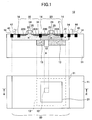
- Figure 1 is a diagram showing the construction of a conventional semiconductor device 10 that uses a MOS transistor 20, wherein the drawing shows the semiconductor device 10 in a plan view in the lower part thereof, while Figure 1 shows a cross-sectional view of the semiconductor device 10 taken along an A-A' line of the plan view in the upper part thereof.
- the plan view it should be noted that some part of the structure shown in the cross-sectional view is omitted.
- the semiconductor device 10 has a construction in which there is formed a device region 21 of p-type in a silicon substrate 11 of p-type such that the device region 21 forms a p-type well defined by a device isolation region 14 of shallow trench isolation (STI) structure. Further, the semiconductor device 20, which may be an n-channel MOS transistor, is formed in the device region 21 thus formed on the substrate 11.
- STI shallow trench isolation
- the n-channel MOS transistor 20 includes a gate insulation film 23 formed on the p-type well 21 and a gate electrode 24 is formed on the gate insulation film 23 in correspondence to a channel region in the p-type well 21.
- the p-type well 21 has an impurity concentration level exceeding the impurity concentration level of the substrate 11.
- diffusion regions 22A and 22B of n-type are formed in p-type well 21 as source and drain regions of the n-channel MOS transistor 20 at respective lateral sides of the gate electrode 24, wherein the source and drain regions 22A and 22B are formed so as to oppose with each other in the p-type well 21 across the channel region formed right underneath the gate electrode 24.
- the diffusion regions 22A and 22B are formed with a reduced depth and reduced impurity concentration level for those parts thereof covered with sidewall insulation films 25 formed on respective sidewall surfaces of the gate electrode 24 and with an increased depth and increased impurity concentration level in those parts not covered with the sidewall insulation films 25.
- the semiconductor device 10 is constructed on a so-called triple well structure, and thus, the p-type well 21 constituting the device region of the n-channel MOS transistor 20 is surrounded laterally by a diffusion region 31 of n - -type. With this, the substrate 11 is substantially divided into the p-type well 21 and remaining p-type region of the substrate 11 by the n - -type diffusion region 31.
- n + -type diffusion region 13 forms, together with the diffusion region 31 of n - -type, a semiconductor isolation structure 50 of n-type surrounding the p-type well 21 at the lateral edge and the bottom edge thereof.
- the terminal 44 is used to control a potential of the well 21 from outside by applying a reverse bias voltage therebetween.
- the semiconductor isolation structure 50 isolates the p-type well 21, and hence the transistor 20 formed thereon, from the remaining p-type region of the substrate 11, which may function as noise source.
- the potential of the p-type substrate 11 is controlled externally by applying a reverse bias to the terminals 42 and 44 as noted above, and the potential of the silicon substrate 11 thus controlled is transmitted to the p-type well 21 via the opening 12.
- a gate insulation film 33 on the diffusion region 31 used for the n-type well and a gate electrode 34 is formed on the gate insulation film 33 in correspondence to a channel region formed in the well 31. Further, diffusion regions 32A and 32B of p-type are formed in the n-type well 31 so as to oppose with each other across the channel region formed right underneath the gate electrode 34.
- sidewall insulation films 35 are formed on the respective sidewall surface of the gate electrode 34, and the source and drain regions 32A and 32B are formed with a reduced depth and reduced impurity concentration level in those parts thereof covered with the sidewall insulation film 35 and with increased depth and increased impurity concentration level in those parts not covered with the insulation film 35.
- the size of the opening 12 has to be reduced as much as possible.
- a more specific object of the present invention is to achieve device miniaturization and decrease of electric power consumption at the same time in a semiconductor device having a transistor of triple-well structure.
- the present invention provides a semiconductor device, comprising:
- the present invention provides a method of fabricating a semiconductor device comprising a semiconductor substrate of a first conductivity type, a well of said first conductivity type formed in said semiconductor substrate, a transistor formed in said well, a diffusion region of a second conductivity type formed in said semiconductor substrate so as to cover a sidewall surface and a bottom surface of said well, a terminal formed on said semiconductor substrate at an outside part of said diffusion region, and a conductive region contacting with said well, said well being in ohmic contact with said conductive region via said semiconductor substrate, said conductive region having an impurity concentration level exceeding an impurity concentration level of said semiconductor substrate, said method comprising the steps of:
- the present invention it becomes possible to achieve miniaturization of the device size and reduction of electric power consumption simultaneously in a semiconductor device having a transistor of triple well structure.
- a semiconductor isolation region around the well on which the transistor is formed, wherein the semiconductor isolation region has a conductivity type opposite to the conductivity type of the well.
- the well is isolated from noise coming from outside of the semiconductor isolation region.
- a semiconductor isolation region includes therein an opening for allowing control of potential of the well from outside.
- the present invention forms a conductive region of first conductivity type in such an opening with high impurity concentration level higher than the impurity concentration level of the substrate.
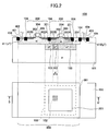
- Figure 2 is a diagram showing a part of a semiconductor device 100 including therein a MOS transistor 200 according to a first embodiment of the present invention, wherein Figure 2 shows, in the bottom part of the drawing, the semiconductor device 100 of the present invention in a plan view, while the top part of Figure 2 shows the same semiconductor device 100 in a cross-sectional view taken along a B-B' line of the plan view.
- Figure 2 shows, in the bottom part of the drawing, the semiconductor device 100 of the present invention in a plan view, while the top part of Figure 2 shows the same semiconductor device 100 in a cross-sectional view taken along a B-B' line of the plan view.
- illustration is omitted for some part of the semiconductor device structure shown in the cross-sectional view.
- the semiconductor device 100 has a construction in which a device 200 such as an n-channel MOS transistor is formed in a device region defined on a substrate 101 of p-type (or a p-type well) by a device isolation region 104 of STI structure, wherein it should be noted that designation "P" provided to the substrate 101 in the drawing does not mean any specific impurity concentration level and it is possible to choose the impurity concentration level for the substrate 101 appropriately.
- the n-channel MOS transistor 200 has a construction such that there is formed a p-type well 201 on the substrate 101 with an impurity concentration level higher than that of the substrate 101, and a gate insulation film 203 is formed on such a p-type well 201 in correspondence to a channel region to be formed therein. Further, a gate electrode 204 is formed on the gate insulation film 203, and source and drain regions 202A and 202B of n-type are formed in the p-type well 201 so as to oppose with each other across the channel region formed underneath the gate electrode 204.
- sidewall insulation films 205 are formed on respective sidewall surfaces of the gate electrode 204, and the source and drain regions 202A and 202B are formed with a shallow depth and smaller impurity concentration level in the part thereof covered by the sidewall insulation films 25 and with increased depth and larger impurity concentration level in the part thereof not covered by the sidewall insulation films 205.
- the semiconductor device 100 uses a so-called triple well structure for eliminating noise from the substrate 101 to the transistor 200, wherein the triple well structure includes the p-type well 201 surrounded by a diffusion region 301 forming an n-type well.
- the p-type substrate 101 is substantially divided into a part that includes therein the p-type well 201 and other p-type part not including the p-type well 201.
- n-type diffusion region forming the n-type well 301 in the silicon substrate 101 in the same plane of the p-type well 201 so as to surround the p-type well 201 laterally, and another n-type well 103 is formed underneath the p-type well 201 in contact with the bottom edge of the p-type well 201 and further the bottom edge of the surrounding n-type well 301, wherein the n-type diffusion region 103 has an impurity concentration level exceeding the impurity concentration level of the n-type well 301 and forms a semiconductor isolation structure 500 together with the n-type well 301 such that the semiconductor isolation structure 500 surrounds the p-type well 201 at the lateral edge and bottom edge thereof.
- the p-type well 201 is isolated from other p-type region of the substrate 101, which may function as noise source.
- a terminal 404 providing a potential to the p-type well 201, such that the terminal 404 is in ohmic contact with the p-type silicon constituting the p-type silicon substrate 101, via a highly-doped p-type contact layer 410 and a metallization layer 403 formed on the contact layer 410.
- a terminal 402 in a part of the diffusion region 301 of n - -type constituting the semiconductor isolation structure 500, wherein the terminal 402 makes an ohmic contact with the diffusion region 301 via a metallization 401 and a contact layer 411 of n + -type formed underneath the metallization 401.
- a conductive region 102 of p + -type so as to extend from the silicon substrate 101 to the p-type well 201, wherein the conductive region 102 transmits the potential provided to the substrate 101 from the terminal 404 to the p-type well 201.
- the potential of the p-type silicon substrate 101 controlled by the bias voltage applied to the terminal 404 is transmitted to the p-type well 201 via the conductive region 102, wherein it should be noted that formation of depletion layer in the conductive region 102 at the p/n junction between the conductive region 102 of p + -type and the diffusion region 103 of n + -type is suppressed effectively because of the increased impurity concentration level in the conductive region 102.
- the semiconductor device 100 of Figure 2 it becomes possible to suppress the occurrence of pinch-off and reduce the electric power consumption even in such a case in which the width d of the conductive region 102 is set to 0.01 - 20 ⁇ m and a reverse bias voltage of 0 - 10V is applied between the conductive region 102 and the isolation region 103, by setting the impurity concentration level of the conductive region 102 to 3 x 10 15 cm -3 or more.
- a p-channel MOS transistor 300 in the n-type diffusion region constituting a part of the isolation region 500.
- a part of the n-type diffusion region 301 is used as the n-type well on which the transistor 300 is formed.
- the MOS transistor is formed on the n-type well 301 formed in the substrate 101 and includes a gate insulation film 303 and a gate electrode 304 is formed on the gate insulation film 303. Further, source and drain regions 302A are formed in the n-type well 301 in the form of p-type diffusion region such that the source and drain regions 302A laterally define the channel region of the p-channel MOS transistor right underneath the gate electrode 304.
- the gate electrode 304 carries sidewall insulation films 305 on respective sidewall surfaces thereof, wherein the source and drain regions 302A and 302B are formed with a reduced depth and reduced impurity concentration level for the part covered by the sidewall insulation films 305 and with increased depth and increased impurity concentration level for the part not covered by the sidewall insulation films 305.
- Figure 3 shows the construction of a semiconductor device 100' according to a modification of the semiconductor device 100, wherein those parts corresponding to the parts described previously are designated by the same reference numerals and the description thereof will be omitted.
- Figure 4 is a diagram showing a part of a semiconductor device 100A including therein the MOS transistor 200 according to a second embodiment of the present invention, wherein Figure 4 shows, in the bottom part of the drawing, the semiconductor device 100A of the present embodiment in a plan view, while the top part of Figure 4 shows the same semiconductor device 100A in a cross-sectional view taken along a C-C' line of the plan view.
- FIG 4 it should be noted that illustration is omitted for some part of the semiconductor device structure shown in the cross-sectional view.
- those parts corresponding to the parts described previously are designated by the same reference numerals and the description thereof will be omitted.
- the semiconductor device 100A forms a conductive region 102A in a part of the semiconductor isolation structure 500 in correspondence to the conductive region 102 of the previous embodiment except that the conductive region 102A has a reduced lateral size as compared with the conductive region 102 of the previous embodiment.
- the area of the conductive region 102A is reduced as compared with the conductive region 102 of the previous embodiment in correspondence to the reduced lateral size thereof.
- the size and shape of the conductive region 102A formed in the semiconductor isolation structure 500 can be changed variously according to the needs.
- Figure 5 is a diagram showing a part of a semiconductor device 100B including therein the MOS transistor 200 according to a third embodiment of the present invention, wherein Figure 5 shows, in the bottom part of the drawing, the semiconductor device 100B of the present embodiment in a plan view, while the top part of Figure 5 shows the same semiconductor device 100B in a cross-sectional view taken along a D-D' line of the plan view.
- Figure 5 shows, in the bottom part of the drawing, the semiconductor device 100B of the present embodiment in a plan view, while the top part of Figure 5 shows the same semiconductor device 100B in a cross-sectional view taken along a D-D' line of the plan view.
- illustration is omitted for some part of the semiconductor device structure shown in the cross-sectional view.
- those parts corresponding to the parts described previously are designated by the same reference numerals and the description thereof will be omitted.
- the present embodiment uses a conductive region 102B of p + -type in correspondence to the conductive region 102 of Figure 2, wherein the conductive region 102B of the present embodiment is formed in introducing a p-type impurity element to a part of the n + -type diffusion region 103B such that the concentration level of the p-type impurity element exceeds the concentration level of the n-type impurity element in the diffusion region 103B.
- the conductive region 102B is formed such that at least a part thereof makes a contact with the p-type well 201.
- the conductive region 102B is formed in correspondence to a boundary of the p-type well 201 and the diffusion region 301 of n - -type, and thus, it will be noted that the conductive region 102B makes a contact with both the p-type well 201 and the n-type diffusion region 301.
- the conductive region 102B has a circular cross-sectional shape contrary to the rectangular cross-sectional shape of the conductive region 102 used with the embodiment of Figure 2, while such a difference in the shape does not influence the effect achieved with the present embodiment.
- various shapes can be used for the conductive region 102B for transmitting the potential of the substrate 101 to the p-type well 201.
- the semiconductor device of the present embodiment it is possible to change the shape and location of the conductive region variously, and large degree of freedom is provided at the time of designing or making layout of the semiconductor device.
- Figure 6 is a diagram showing a semiconductor device 100C according to a modification of the semiconductor device 100B of the present embodiment, wherein those parts corresponding to the parts described previously are designated by the same reference numerals and the description thereof will be omitted.
- the conductive region 102C corresponding to the conductive region 102B of Figure 2 is formed with an increased size with the semiconductor device 100C of Figure 6. Further, with reference to the plan view, it will be noted that the conductive region 102C is provided at a location different from that of the conductive region 102B. Further, it will be noted that the conductive region 102C is distinct over the conductive region 102 in that the conductive region 102C has a rounded rectangular shape when viewed in a plan view diagram. With such a construction, too, the conductive region 102C can function similarly to the conductive region 102B.
- n-type diffusion region 103B can be formed with various shapes and sizes with the present embodiment.
- the diffusion region 103 may be formed over the entire substrate surface.
- Figure 7 is a diagram showing a part of a semiconductor device 100C including therein the MOS transistor 200 according to a fourth embodiment of the present invention, wherein those parts corresponding to the parts described previously are designated by the same reference numerals and the description thereof will be omitted.
- the diffusion region 103 of n + -type is formed over a wide area with the semiconductor device 100D of the present embodiment as compared with the semiconductor device 100 explained with reference to Figure 2, and thus, the diffusion region 103 extends over an area larger than the area of the diffusion region 102 of the device 100 of Figure 2.
- the diffusion region 410 is formed on a diffusion region 405 of p-type formed with the same fabrication process of the p-type well and thus have the impurity concentration level identical with the impurity concentration level of the p-type well 201, wherein the p-type diffusion region 405 is formed on a p-type diffusion region 406 having an impurity concentration level exceeding the impurity concentration level of the diffusion region 405.
- the diffusion region 406 is formed with the same fabrication process of the conductive region 102, and thus, the impurity diffusion region 406 and the conductive region have the same impurity concentration level.
- diffusion regions 407 and 408 of n-type respectively at a side away from the MOS transistor 200 there are formed diffusion regions 407 and 408 of n-type respectively at a side away from the MOS transistor 200, wherein the diffusion regions 407 and 408 are formed so as to isolate the p-type diffusion regions 405 and 406, respectively.
- the n-type diffusion region 407 is formed in the same fabrication process of the n-type diffusion region 301, and the n-type diffusion region 408 is formed in the same fabrication process of the n-type diffusion region 103.
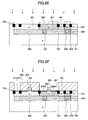
- step of Figure 8A formation of the device isolation structure 104 of STI structure is conducted on the silicon substrate 101 of p-type, and ion implantation process of a p-type impurity element is conducted in the step of Figure 8B into the substrate 101 while using a resist pattern 501 formed on the silicon substrate 101 as a mask.
- the conductive region 102 and the p-type diffusion region 406 are formed simultaneously in the form of highly doped p-type diffusion region.
- the resist pattern 501 is removed, and a resist pattern 502 is formed on the substrate 102 so as to cover the region where the conductive region 102 and the p-type diffusion region 406 are formed. Further, an ion implantation process of an n-type element is conducted into the silicon substrate 101 not covered with the resist pattern 502, and there are formed highly doped n-type diffusion regions as the n-type diffusion regions 103 and 408.
- the conductive region 102 and the p-type diffusion region 406 are formed with the same impurity concentration level, and the n-type diffusion region 103 and the n-type diffusion region 408 are formed with the same impurity concentration level.
- the conductive region 102, the p-type diffusion region 406, the n-type diffusion region 103 and the n-type diffusion region 408 are formed substantially on the same plane.
- a resist pattern 503 is formed on the substrate 101 and ion implantation of a p-type impurity element is conducted, and with this, the p-type well 201 and the p-type diffusion region 405 of p - -type are formed in the silicon substrate 101 in correspondence to the opening of the resist pattern 503, wherein the p - -type well 201 and the p - -type diffusion region 405 thus formed have an impurity concentration level higher than that of the silicon substrate 101, while the impurity concentration level of the p - -type well 201 and the p--type diffusion regions 405 is lower than that of the p + -type conductive region 102 and the p + -type diffusion region 406.
- the resist pattern 503 is removed, and a new resist pattern 504 is formed on the silicon substrate 101 so as to cover the p-type well and the p-type diffusion region 405. Further, by conducting an ion implantation process of an n-type impurity element in this state, the diffusion regions 301 and 407 of n - -type are formed in correspondence to the part of the silicon substrate 101 not covered with the resist pattern 504. Thus, the n-type diffusion regions 301 and 407 have a lower impurity concentration level as compared with the n-type diffusion regions 103 and 408.
- the p-type well 201 and the p-type diffusion region 405 have the same impurity concentration level, and n-type diffusion region 301 and the n-type diffusion region 407 have the same impurity concentration level. It should be noted that the p-type well 201, the p-type diffusion region 405, the n-type diffusion region 301 and the n-type diffusion region 407 are formed a substantially in the same plane in the silicon substrate 101.
- the resist pattern 504 is removed, and a gate insulation film is formed on the p-type well 201 and further on the n-type diffusion region 301. Further, by depositing and patterning a polysilicon layer on the gate insulation film thus formed, the gate electrode 204 is formed on the p-type well 201 via the gate insulation film 203 and the gate electrode 304 is formed on the n-type well 301 via the gate insulation film 303.
- a resist pattern 505 is formed on the silicon substrate 101 with resist openings corresponding to the p-type well 201 and the n-type diffusion region 411, and ion implantation process of an n-type impurity element is conducted into the substrate 101 while using the resist pattern 505 as a mask.
- the source and drain regions 202A and 202B are formed in the p-type well 201 and an n + -type diffusion region is formed as the contact layer 411.
- the resist pattern 505 is removed and a new resist pattern 506 is formed on the silicon substrate such that the resist pattern 506 forms resist openings in correspondence to the n-type well to be formed in the n-type diffusion region 301 as the device region of the p-channel MOS transistor 300 and the p-type diffusion region 410. Further, by conducting an ion implantation process of a p-type impurity element while using the resist pattern 506 as a mask, the source and drain regions 302A of p + -type are formed in the n-type well 301 and the p+-type contact region 410 is formed on the p-type region 405.
- the resist pattern 506 is removed, and the sidewall insulation films 205 and 305 are formed on the respective sidewall surfaces of the gate electrodes 204 and 304.
- the source and drain regions 202A and 202B are formed with reduced depth in the part closer to the gate electrode 204 and covered with the sidewall insulation films 205 and increased depth in the part far from the gate electrode 304 and not covered with the sidewall insulation films 205.
- the source and drain regions 302A and 302B are formed with reduced depth in the part closer to the gate electrode 304 and covered with the sidewall insulation films 305 and increased depth in the part far from the gate electrode 304 and not covered with the sidewall insulation films 305.
- the metallization layers 401 and 403 are formed, and with formation of the terminals 402 and 404, the semiconductor device 100D shown in Figure 7 is obtained.
- an interlayer insulation film is formed according to the needs, and a multilayer interconnection structure is formed on the transistors thus formed.
- the present invention is by no means limited to such a process and it is possible to form the conductive region 102 after formation of the n-type diffusion region 103.
- a resist pattern 502A is formed on the silicon substrate 101, and the n-type diffusion region 103 is formed in the silicon substrate 101 by conducting an ion implantation process of an n-type impurity element into the substrate 101 while using the resist pattern 502 as a mask.
- the resist pattern 502A is removed, and a resist pattern 501A is formed on the substrate 101 so as to cover a part thereof corresponding to the diffusion region 103.
- the conductive region 102 of highly doped p-type region is formed in the part not covered with the resist pattern 501A by conducting an ion implantation process of a p-type impurity element.
- the resist pattern 501 shown in Figure 8B and the resist pattern 502 shown in Figure 8C are in a reversal relationship in that the part covering the substrate and the part forming a resist opening are reversed from each other.
- Figures 10A and 10B those parts corresponding to the parts explained before with reference to the fourth embodiment are designated by the same reference numerals and the description thereof will be omitted.
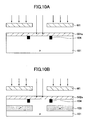
- Figure 10A shows an example of formation of the resist pattern 501 shown in Figure 8B.
- a mask pattern M1 exposing a part corresponding to the resist opening of the resist pattern 501 is used for exposing a positive resist film 501a, and thus, the resist pattern 501 shown in Figure 8B is obtained after development of the resist film 501a thus exposed.
- Figure 10B shows an example of formation of the resist pattern 502 shown in Figure 8C.
- a mask pattern M1 exposing a part of the resist pattern 502 covering the substrate is used for exposing a negative resist film 502a, and the resist pattern shown in Figure 8C is obtained after development of the resist film 502a thus exposed.
- Figures 11A and 11B are diagrams showing the fabrication process of a semiconductor device according to a seventh embodiment of the present invention, wherein those parts corresponding to he parts described previously with preceding embodiments are designated by the same reference numerals and the description thereof will be omitted.
- an n-type impurity element is introduced into the part of the silicon substrate 101 by an ion implantation process to form an n+-type diffusion layer 103B' of high impurity concentration level in the part where the n-type diffusion region 103B is to be formed including the region of the conductive region 102.
- a resist pattern 507 is formed on the silicon substrate 101 so as to cover the part thereof in which the n-type diffusion region 103B is to be formed, and ion implantation process of a p-type impurity element is conducted.
- the conductive region 102B of p +- type is formed in the part not covered with the resist pattern 507, while remaining region of the n + -type diffusion region 103B' forms the diffusion region 103.
- Figures 12A and 12B are diagrams showing the fabrication process of a semiconductor device according to an eighth embodiment of the present invention, wherein those parts corresponding to the parts described previously are designated by the same reference numerals and the description thereof will be omitted.
- a diffusion region 102B' of p + -type by introducing a p-type impurity element into the silicon substrate 101 with high concentration level including the region in which the conductive region 102B is to be formed, and in the step of Figure 12B, there is conducted an ion implantation process of an n-type impurity element into the silicon substrate 101 while covering the part of the silicon substrate 101 corresponding to the conducive region 102B by providing a resist pattern 508.
- the diffusion region 103B of n + -type is formed in the part not covered with the resist pattern 508, while the part of the p + -type diffusion region 102B' not formed with the diffusion region 103B of n + -type forms the conductive region 102B of p + -type.
- Figure 13 shows the construction of a semiconductor device used for investigating the effect of the present invention.
- the semiconductor device has a structure similar to that of the semiconductor device 100 explained with reference to Figure 2 except that source and drain regions, gate insulation film and gate electrode are eliminated.
- the semiconductor device of Figure 13 is constructed on a silicon substrate 901 of p-type and includes therein a well 904 of p - -type defined by a device isolation region 906 of STI structure and surrounded laterally by a diffusion region 905 of n - -type, wherein there is provided a diffusion region of n + -type underneath the p-type well 904 and the surrounding diffusion region 905 of n-type.
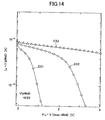
- the potential of the p-type well is fixed at 0.5V, and the current Ip flowing to the well 904 is investigated while changing the voltage Vn of the n-type diffusion region 903.
- Figure 14 shows the result of this investigation, wherein it will be noted that the experiment have been conductive for different impurity concentration levels for the conductive region 902 as represented by experiments EX1, EX2 and EX3.
- Experiment EX1 uses the same impurity concentration level of the substrate 901 for the conductive region 902, and thus, this experiment corresponds to the semiconductor device of conventional art.
- the impurity concentration level of the conductive region 902 is increased over the impurity concentration level of the substrate 901, while in the case of experiment EX3, the impurity concentration level of the conductive region 902 is increased further as compared with the case of experiment EX2.
Landscapes
- Metal-Oxide And Bipolar Metal-Oxide Semiconductor Integrated Circuits (AREA)
- Element Separation (AREA)
- Insulated Gate Type Field-Effect Transistor (AREA)
Abstract
Description
- The present application is based on
Japanese priority application No.2005-096276 filed on March 29, 2005 - The present invention generally relates to semiconductor devices and fabrication process thereof and more particularly to a semiconductor device including a field effect transistor and fabrication process thereof.
- With demand for improvement of performance in semiconductor devices in recent years, there is also a demand of improved performance in the field effect transistors (FET) such as a metal-oxide-semiconductor (MOS) transistor used in such semiconductor devices. Typically, a MOS transistor has a structure in which a source region and a drain regions are formed in a diffusion layer called well formed in a semiconductor substrate in the form of diffusion regions of opposite conductivity type.
- In order to improve the resistance of such MOS transistors against noise, there is proposed the use of a so-called triple well structure in which a well used for a device region is formed in a substrate in a manner surrounded by an impurity diffusion region of opposite conductivity type. With such a structure, the well forming the device region is isolated from the influence of other circuits or the semiconductor substrate itself.
- In this technology of triple well, it is proposed to provide a terminal outside the triple well and control the potential of the well inside the triple well via a conduction region formed so as to conduct the interior of the triple well with the external terminal (Patent Reference 1).
-
Patent Reference 1Japanese Laid-Open Patent Application 10- 199993 - Figure 1 is a diagram showing the construction of a
conventional semiconductor device 10 that uses aMOS transistor 20, wherein the drawing shows thesemiconductor device 10 in a plan view in the lower part thereof, while Figure 1 shows a cross-sectional view of thesemiconductor device 10 taken along an A-A' line of the plan view in the upper part thereof. In the plan view, it should be noted that some part of the structure shown in the cross-sectional view is omitted. - Referring to Figure 1, the
semiconductor device 10 has a construction in which there is formed adevice region 21 of p-type in asilicon substrate 11 of p-type such that thedevice region 21 forms a p-type well defined by adevice isolation region 14 of shallow trench isolation (STI) structure. Further, thesemiconductor device 20, which may be an n-channel MOS transistor, is formed in thedevice region 21 thus formed on thesubstrate 11. - More specifically, the n-
channel MOS transistor 20 includes agate insulation film 23 formed on the p-type well 21 and agate electrode 24 is formed on thegate insulation film 23 in correspondence to a channel region in the p-type well 21. Typically, the p-type well 21 has an impurity concentration level exceeding the impurity concentration level of thesubstrate 11. - Further,
diffusion regions type well 21 as source and drain regions of the n-channel MOS transistor 20 at respective lateral sides of thegate electrode 24, wherein the source anddrain regions type well 21 across the channel region formed right underneath thegate electrode 24. Thereby, thediffusion regions sidewall insulation films 25 formed on respective sidewall surfaces of thegate electrode 24 and with an increased depth and increased impurity concentration level in those parts not covered with thesidewall insulation films 25. - In order to improve the robustness of the
transistor 20 against noise from thesubstrate 101, thesemiconductor device 10 is constructed on a so-called triple well structure, and thus, the p-type well 21 constituting the device region of the n-channel MOS transistor 20 is surrounded laterally by adiffusion region 31 of n--type. With this, thesubstrate 11 is substantially divided into the p-type well 21 and remaining p-type region of thesubstrate 11 by the n--type diffusion region 31. - Further, there is formed a
diffusion region 13 of n+-type further underneath the p-type well 21 in contact with a bottom edge thereof and further a bottom edge of the n--typewell diffusion region 31 laterally surrounding the p-type well 21. Thereby, the n+-type diffusion region 13 forms, together with thediffusion region 31 of n--type, asemiconductor isolation structure 50 of n-type surrounding the p-type well 21 at the lateral edge and the bottom edge thereof. - Further, it should be noted that there is provided a
terminal 44 in the part of thesubstrate 11 outside the p-type well 21 with thesemiconductor device 10 such that theterminal 44 is connected to a p-type part of thesubstrate 11 via acontact layer 43 of p+-type, wherein there is provided anotherterminal 42 in a part of the n--type diffusion region 31 via acontact layer 41 of n+-type. It should be noted that theterminal 44 is used to control a potential of thewell 21 from outside by applying a reverse bias voltage therebetween. - With such a construction, the
semiconductor isolation structure 50 isolates the p-type well 21, and hence thetransistor 20 formed thereon, from the remaining p-type region of thesubstrate 11, which may function as noise source. - In order to allow control of potential of the p-
type well 21 from theterminal 44, there is formed an "opening" 12 in thesemiconductor isolation structure 50 at the bottom part thereof, more specifically in thediffusion layer 13 of n+-type, wherein the "opening" 12 is in fact a region of the p-type silicon substrate 11 not formed with thediffusion region 13 of n+-type and thus has the impurity concentration level substantially identical with the impurity concentration level of thesilicon substrate 11. Thereby, the potential of the p-type substrate 11 is controlled externally by applying a reverse bias to theterminals silicon substrate 11 thus controlled is transmitted to the p-type well 21 via theopening 12. - With the construction of Figure 1, there is further provided a p-
channel MOS transistor 30 in thediffusion region 31 of n-type, which constitutes a part of thesemiconductor isolation structure 50, while using thediffusion region 31 as an n-type well. - In the
transistor 30, it should be noted that there is formed agate insulation film 33 on thediffusion region 31 used for the n-type well and agate electrode 34 is formed on thegate insulation film 33 in correspondence to a channel region formed in thewell 31. Further,diffusion regions type well 31 so as to oppose with each other across the channel region formed right underneath thegate electrode 34. - With such a construction,
sidewall insulation films 35 are formed on the respective sidewall surface of thegate electrode 34, and the source anddrain regions sidewall insulation film 35 and with increased depth and increased impurity concentration level in those parts not covered with theinsulation film 35. - On the other hand, with advanced semiconductor devices of these days, there is imposed a severe demand of device miniaturization in addition to the demand of reducing the electric power consumption, and associated with this, there have been caused various problems with the semiconductor devices constructed on a triple well structure.
- From the viewpoint of reducing the electric power consumption, it is desirable to apply as large bias voltage as possible across the
terminals type well 21 and thesemiconductor isolation structure 50 are controllable over wide range from a zero bias state to large reverse bias state. On the other hand, from the viewpoint of miniaturization of the semiconductor device, the size of theopening 12 has to be reduced as much as possible. - Thus, in the case there is applied a large reverse bias voltage across the
electrodes opening 12 is reduced, extension of the depletion layer formed in theopening 12 at the p/n junction between the p--type semiconductor constituting the opening 12 and the n+-type diffusion region 13 is no longer ignorable with regard to the size of theopening 12, and it becomes difficult to transmit the potential of thesubstrate 11 controlled by theelectrode 44 to the p-type well 21 via theopening 12. Depending on the magnitude of the potential difference and the size of the opening 12, there is even a possibility that a complete pinch-off is caused at theopening 12. - Thus, with the semiconductor device having a transistor constructed on a triple-well structure, there have been cases in which it becomes difficult to achieve both device miniaturization and reduction of electric power consumption simultaneously.
- Accordingly, it is a general object of the present invention to provide a novel and useful semiconductor device and fabrication process thereof wherein the foregoing problems are eliminated.
- A more specific object of the present invention is to achieve device miniaturization and decrease of electric power consumption at the same time in a semiconductor device having a transistor of triple-well structure.
- In a first aspect, the present invention provides a semiconductor device, comprising:
- a semiconductor substrate of a first conductivity type;
- a well of said first conductivity type formed in said semiconductor substrate;
- a transistor formed in said well;
- a diffusion region of a second conductivity type formed in said semiconductor substrate so as to cover a lateral side and a bottom edge of said well;
- a terminal formed on said semiconductor substrate at an outside part of said diffusion region; and
- a conductive region contacting with said well,
- said well being in ohmic contact with said terminal via said conductive region and said semiconductor substrate,
- said conductive region having an impurity concentration level exceeding an impurity concentration level of said semiconductor substrate.
- According to the present invention, it is possible to achieve miniaturization and reduction of electric power consumption simultaneously in a semiconductor device that includes a transistor of triple well structure.
- According to a second aspect, the present invention provides a method of fabricating a semiconductor device comprising a semiconductor substrate of a first conductivity type, a well of said first conductivity type formed in said semiconductor substrate, a transistor formed in said well, a diffusion region of a second conductivity type formed in said semiconductor substrate so as to cover a sidewall surface and a bottom surface of said well, a terminal formed on said semiconductor substrate at an outside part of said diffusion region, and a conductive region contacting with said well, said well being in ohmic contact with said conductive region via said semiconductor substrate, said conductive region having an impurity concentration level exceeding an impurity concentration level of said semiconductor substrate, said method comprising the steps of:
- forming a conductive region in said semiconductor substrate by introducing a first impurity element of a first conductivity type; and
- forming said diffusion region by introducing a second impurity element of second conductivity type into said semiconductor substrate.
- According to the present invention, it becomes possible to achieve miniaturization of the device size and reduction of electric power consumption simultaneously in a semiconductor device having a transistor of triple well structure.
- Other objects and further features of the present invention will become apparent from the following detailed description when read in conjunction with the attached drawings.
-
- Figure 1 is a diagram showing the construction of a conventional semiconductor device;
- Figure 2 is a diagram showing the construction of a semiconductor device according to a first embodiment of the present invention;
- Figure 3 is a diagram showing a modification of the semiconductor device of the second embodiment;
- Figure 4 is a diagram showing the construction of a semiconductor device according to a second embodiment of the present invention;
- Figure 5 is a diagram showing the construction of a semiconductor device according to a third embodiment of the present invention;
- Figure 6 is a diagram showing a modification of the semiconductor device of Figure 5;
- Figure 7 is a diagram showing the construction of a semiconductor device according to a fourth embodiment of the present invention;
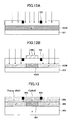
- Figures 8A - 8G are diagrams showing the fabrication process of the semiconductor device of Figure 7;
- Figures 9A and 9B are diagrams showing the fabrication process of a semiconductor device according to a fifth embodiment of the present invention;
- Figures 10A and 10B are diagrams showing the fabrication process of a semiconductor device according to a sixth embodiment of the present invention;
- Figures 11A and 11B are diagrams showing the fabrication process of a semiconductor device according to a seventh embodiment of the present invention;
- Figures 12A and 12B are diagrams showing the fabrication process of a semiconductor device according to an eighth embodiment of the present invention;
- Figure 13 is a diagram showing the construction of a test device used for investigating the effect of the present invention;
- Figure 14 is a diagram showing the electric characteristics of the test device of Figure 13.
- With the present invention, it becomes possible to achieve the object of reduction of electric power consumption and device miniaturization at the same time in a transistor constructed on a triple well structure.
- With the transistor constructed on a triple well structure, there is formed a semiconductor isolation region around the well on which the transistor is formed, wherein the semiconductor isolation region has a conductivity type opposite to the conductivity type of the well. Thereby, the well is isolated from noise coming from outside of the semiconductor isolation region. Further, such a semiconductor isolation region includes therein an opening for allowing control of potential of the well from outside.
- In order to reduce the electric power consumption while achieving device miniaturization at the same time with such a semiconductor device constructed on a triple well structure, it is desirable to apply a large reverse bias voltage across the semiconductor isolation region and the well while decreasing the size of the opening at the same time. Thereby, there is a concern that the depletion region formed in the opening as a result of the reverse biasing may no longer be ignorable and that there may be caused a pinch-off phenomenon in such an opening as a result of such a large reverse biasing.
- In view of the foregoing, the present invention forms a conductive region of first conductivity type in such an opening with high impurity concentration level higher than the impurity concentration level of the substrate.
- With such a construction, extension of the depletion region in the opening is effectively suppressed, and it becomes possible to achieve reduction of electric power consumption and device miniaturization at the same time with the transistor constructed on such a triple well structure.
- Hereinafter, the present invention will be explained with reference to embodiments.
- Figure 2 is a diagram showing a part of a
semiconductor device 100 including therein aMOS transistor 200 according to a first embodiment of the present invention, wherein Figure 2 shows, in the bottom part of the drawing, thesemiconductor device 100 of the present invention in a plan view, while the top part of Figure 2 shows thesame semiconductor device 100 in a cross-sectional view taken along a B-B' line of the plan view. In the plan view of Figure 2, it should be noted that illustration is omitted for some part of the semiconductor device structure shown in the cross-sectional view. - Referring to Figure 2, the
semiconductor device 100 has a construction in which adevice 200 such as an n-channel MOS transistor is formed in a device region defined on asubstrate 101 of p-type (or a p-type well) by adevice isolation region 104 of STI structure, wherein it should be noted that designation "P" provided to thesubstrate 101 in the drawing does not mean any specific impurity concentration level and it is possible to choose the impurity concentration level for thesubstrate 101 appropriately. - The n-
channel MOS transistor 200 has a construction such that there is formed a p-type well 201 on thesubstrate 101 with an impurity concentration level higher than that of thesubstrate 101, and agate insulation film 203 is formed on such a p-type well 201 in correspondence to a channel region to be formed therein. Further, agate electrode 204 is formed on thegate insulation film 203, and source anddrain regions gate electrode 204. - Further,
sidewall insulation films 205 are formed on respective sidewall surfaces of thegate electrode 204, and the source anddrain regions sidewall insulation films 25 and with increased depth and larger impurity concentration level in the part thereof not covered by thesidewall insulation films 205. - The
semiconductor device 100 uses a so-called triple well structure for eliminating noise from thesubstrate 101 to thetransistor 200, wherein the triple well structure includes the p-type well 201 surrounded by adiffusion region 301 forming an n-type well. Thereby, the p-type substrate 101 is substantially divided into a part that includes therein the p-type well 201 and other p-type part not including the p-type well 201. - More specifically, in the structure of Figure 2, there is further formed an n-type diffusion region forming the n-type well 301 in the
silicon substrate 101 in the same plane of the p-type well 201 so as to surround the p-type well 201 laterally, and another n-type well 103 is formed underneath the p-type well 201 in contact with the bottom edge of the p-type well 201 and further the bottom edge of the surrounding n-type well 301, wherein the n-type diffusion region 103 has an impurity concentration level exceeding the impurity concentration level of the n-type well 301 and forms asemiconductor isolation structure 500 together with the n-type well 301 such that thesemiconductor isolation structure 500 surrounds the p-type well 201 at the lateral edge and bottom edge thereof. - Thus, with formation of the
semiconductor isolation structure 500, the p-type well 201 is isolated from other p-type region of thesubstrate 101, which may function as noise source. - Further, it should be noted that, in the outside region of the p-type well 201 isolated therefrom by the
semiconductor isolation structure 500, there is formed a terminal 404 providing a potential to the p-type well 201, such that the terminal 404 is in ohmic contact with the p-type silicon constituting the p-type silicon substrate 101, via a highly-doped p-type contact layer 410 and ametallization layer 403 formed on thecontact layer 410. - Similarly, there is provided a terminal 402 in a part of the
diffusion region 301 of n--type constituting thesemiconductor isolation structure 500, wherein the terminal 402 makes an ohmic contact with thediffusion region 301 via ametallization 401 and acontact layer 411 of n+-type formed underneath themetallization 401. - Further, at the bottom part of the
semiconductor isolation structure 500, more specifically, in a part of the n-type region 103, there is formed aconductive region 102 of p+-type so as to extend from thesilicon substrate 101 to the p-type well 201, wherein theconductive region 102 transmits the potential provided to thesubstrate 101 from the terminal 404 to the p-type well 201. - Thus, by applying a reverse bias voltage across the
terminals type silicon substrate 101 controlled by the bias voltage applied to the terminal 404 is transmitted to the p-type well 201 via theconductive region 102, wherein it should be noted that formation of depletion layer in theconductive region 102 at the p/n junction between theconductive region 102 of p+-type and thediffusion region 103 of n+-type is suppressed effectively because of the increased impurity concentration level in theconductive region 102. Thereby, it becomes possible to apply a large reverse bias voltage across theterminals type well 201 and thesemiconductor isolation structure 500 while minimizing extension of the depletion layer. - Thus, with the present invention, it becomes possible to achieve device miniaturization and reduction of electric power consumption at the same time in the semiconductor device that uses a transistor formed on triple well structure.
- For example, with the
semiconductor device 100 of Figure 2, it becomes possible to suppress the occurrence of pinch-off and reduce the electric power consumption even in such a case in which the width d of theconductive region 102 is set to 0.01 - 20µm and a reverse bias voltage of 0 - 10V is applied between theconductive region 102 and theisolation region 103, by setting the impurity concentration level of theconductive region 102 to 3 x 1015cm-3 or more. Particularly, it is advantageous to suppress the occurrence of depletion layer when the difference of impurity concentration level between thesubstrate 101 and theconductive region 102 is equal to or larger than 3 x 1015cm-3. - In the construction of the present embodiment, it is also possible to form a p-
channel MOS transistor 300 in the n-type diffusion region constituting a part of theisolation region 500. In this case, a part of the n-type diffusion region 301 is used as the n-type well on which thetransistor 300 is formed. - More specifically, the MOS transistor is formed on the n-type well 301 formed in the
substrate 101 and includes agate insulation film 303 and agate electrode 304 is formed on thegate insulation film 303. Further, source anddrain regions 302A are formed in the n-type well 301 in the form of p-type diffusion region such that the source anddrain regions 302A laterally define the channel region of the p-channel MOS transistor right underneath thegate electrode 304. - Thereby, the
gate electrode 304 carriessidewall insulation films 305 on respective sidewall surfaces thereof, wherein the source anddrain regions sidewall insulation films 305 and with increased depth and increased impurity concentration level for the part not covered by thesidewall insulation films 305. - Figure 3 shows the construction of a semiconductor device 100' according to a modification of the
semiconductor device 100, wherein those parts corresponding to the parts described previously are designated by the same reference numerals and the description thereof will be omitted. - Referring to Figure 3, it will be noted that no transistor is formed in a diffusion region 301' of n-type corresponding to the
diffusion region 300 with the semiconductor device 100', wherein the diffusion region 301' functions as a part of a semiconductor isolation structure 500' corresponding to thesemiconductor isolation structure 500 of FIG.2. In this modification, it is possible to form a well for another transistor adjacent to the n-type diffusion region 301'. - Figure 4 is a diagram showing a part of a
semiconductor device 100A including therein theMOS transistor 200 according to a second embodiment of the present invention, wherein Figure 4 shows, in the bottom part of the drawing, thesemiconductor device 100A of the present embodiment in a plan view, while the top part of Figure 4 shows thesame semiconductor device 100A in a cross-sectional view taken along a C-C' line of the plan view. In the plan view of Figure 4, it should be noted that illustration is omitted for some part of the semiconductor device structure shown in the cross-sectional view. In Figure 4, those parts corresponding to the parts described previously are designated by the same reference numerals and the description thereof will be omitted. - Referring to Figure 4, the
semiconductor device 100A forms aconductive region 102A in a part of thesemiconductor isolation structure 500 in correspondence to theconductive region 102 of the previous embodiment except that theconductive region 102A has a reduced lateral size as compared with theconductive region 102 of the previous embodiment. - In the plan view, it will be noted that the area of the
conductive region 102A is reduced as compared with theconductive region 102 of the previous embodiment in correspondence to the reduced lateral size thereof. - With the construction of the present embodiment, there is formed a p-type region of reduced impurity concentration level between the p+-type
conductive region 102A and thediffusion region 103 of n+-type with an impurity concentration level lower than that of theconductive region 102A, such as the impurity concentration level of thesilicon substrate 101. - With such a construction, it is possible to reduce the parasitic capacitance between the
conductive region 102A and thediffusion region 103. - Thus, it should be noted that the size and shape of the
conductive region 102A formed in thesemiconductor isolation structure 500 can be changed variously according to the needs. - Figure 5 is a diagram showing a part of a
semiconductor device 100B including therein theMOS transistor 200 according to a third embodiment of the present invention, wherein Figure 5 shows, in the bottom part of the drawing, thesemiconductor device 100B of the present embodiment in a plan view, while the top part of Figure 5 shows thesame semiconductor device 100B in a cross-sectional view taken along a D-D' line of the plan view. In the plan view of Figure 5, it should be noted that illustration is omitted for some part of the semiconductor device structure shown in the cross-sectional view. In Figure 5, those parts corresponding to the parts described previously are designated by the same reference numerals and the description thereof will be omitted. - Referring to Figure 5, it will be noted that there is formed a
diffusion region 103B of n-type corresponding to the n-type diffusion region 103 of Figure 2 such that thediffusion region 103B extends over a wide area of thesubstrate 101. - Further, the present embodiment uses a
conductive region 102B of p+-type in correspondence to theconductive region 102 of Figure 2, wherein theconductive region 102B of the present embodiment is formed in introducing a p-type impurity element to a part of the n+-type diffusion region 103B such that the concentration level of the p-type impurity element exceeds the concentration level of the n-type impurity element in thediffusion region 103B. - Here, it should be noted that the
conductive region 102B is formed such that at least a part thereof makes a contact with the p-type well 201. In the present embodiment, for example, theconductive region 102B is formed in correspondence to a boundary of the p-type well 201 and thediffusion region 301 of n--type, and thus, it will be noted that theconductive region 102B makes a contact with both the p-type well 201 and the n-type diffusion region 301. - It should be noted further that the
conductive region 102B has a circular cross-sectional shape contrary to the rectangular cross-sectional shape of theconductive region 102 used with the embodiment of Figure 2, while such a difference in the shape does not influence the effect achieved with the present embodiment. - Thus, various shapes can be used for the
conductive region 102B for transmitting the potential of thesubstrate 101 to the p-type well 201. - With the present embodiment, it should be noted that application of potential to the
substrate 101 is achieved differently over the previous embodiments in that there is formed acontact layer 101A of highly doped p-type at the rear side of thesubstrate 101 and a terminal 101B is provided to thecontact layer 101A thus formed for application of the potential. Thereby, the terminal 101B functions similarly to theterminal 404 of the previous embodiments. In this way, various embodiments are possible for the terminal 404 used for applying a potential to the p-type well 201. - Thus, with the semiconductor device of the present embodiment, it is possible to change the shape and location of the conductive region variously, and large degree of freedom is provided at the time of designing or making layout of the semiconductor device.
- Figure 6 is a diagram showing a
semiconductor device 100C according to a modification of thesemiconductor device 100B of the present embodiment, wherein those parts corresponding to the parts described previously are designated by the same reference numerals and the description thereof will be omitted. - Referring to Figure 6, it will be noted that the
conductive region 102C corresponding to theconductive region 102B of Figure 2 is formed with an increased size with thesemiconductor device 100C of Figure 6. Further, with reference to the plan view, it will be noted that theconductive region 102C is provided at a location different from that of theconductive region 102B. Further, it will be noted that theconductive region 102C is distinct over theconductive region 102 in that theconductive region 102C has a rounded rectangular shape when viewed in a plan view diagram. With such a construction, too, theconductive region 102C can function similarly to theconductive region 102B. - Further, it should be noted that the n-
type diffusion region 103B can be formed with various shapes and sizes with the present embodiment. For example, thediffusion region 103 may be formed over the entire substrate surface. - Figure 7 is a diagram showing a part of a
semiconductor device 100C including therein theMOS transistor 200 according to a fourth embodiment of the present invention, wherein those parts corresponding to the parts described previously are designated by the same reference numerals and the description thereof will be omitted. - Referring to Figure 7, the
diffusion region 103 of n+-type is formed over a wide area with thesemiconductor device 100D of the present embodiment as compared with thesemiconductor device 100 explained with reference to Figure 2, and thus, thediffusion region 103 extends over an area larger than the area of thediffusion region 102 of thedevice 100 of Figure 2. - Further, the
diffusion region 410 is formed on adiffusion region 405 of p-type formed with the same fabrication process of the p-type well and thus have the impurity concentration level identical with the impurity concentration level of the p-type well 201, wherein the p-type diffusion region 405 is formed on a p-type diffusion region 406 having an impurity concentration level exceeding the impurity concentration level of thediffusion region 405. Thereby, thediffusion region 406 is formed with the same fabrication process of theconductive region 102, and thus, theimpurity diffusion region 406 and the conductive region have the same impurity concentration level. - Further, in the outer side of the p-
type diffusion region 405 and hence in the p-type diffusion region 406, there are formeddiffusion regions MOS transistor 200, wherein thediffusion regions type diffusion regions - Thereby, it should be noted that the n-
type diffusion region 407 is formed in the same fabrication process of the n-type diffusion region 301, and the n-type diffusion region 408 is formed in the same fabrication process of the n-type diffusion region 103. - Next, fabrication process of the
semiconductor device 100D will be explained with reference to Figures 8A - 8H, wherein those parts corresponding to the parts described previously are designated by the same reference numerals and the description thereof will be omitted. - First, in the step of Figure 8A, formation of the
device isolation structure 104 of STI structure is conducted on thesilicon substrate 101 of p-type, and ion implantation process of a p-type impurity element is conducted in the step of Figure 8B into thesubstrate 101 while using a resistpattern 501 formed on thesilicon substrate 101 as a mask. Thereby, theconductive region 102 and the p-type diffusion region 406 are formed simultaneously in the form of highly doped p-type diffusion region. - Next, in the step of Figure 8C, the resist
pattern 501 is removed, and a resistpattern 502 is formed on thesubstrate 102 so as to cover the region where theconductive region 102 and the p-type diffusion region 406 are formed. Further, an ion implantation process of an n-type element is conducted into thesilicon substrate 101 not covered with the resistpattern 502, and there are formed highly doped n-type diffusion regions as the n-type diffusion regions conductive region 102 and the p-type diffusion region 406 are formed with the same impurity concentration level, and the n-type diffusion region 103 and the n-type diffusion region 408 are formed with the same impurity concentration level. - Further, the
conductive region 102, the p-type diffusion region 406, the n-type diffusion region 103 and the n-type diffusion region 408 are formed substantially on the same plane. - Next, in the step of Figure 8D, a resist
pattern 503 is formed on thesubstrate 101 and ion implantation of a p-type impurity element is conducted, and with this, the p-type well 201 and the p-type diffusion region 405 of p--type are formed in thesilicon substrate 101 in correspondence to the opening of the resistpattern 503, wherein the p--type well 201 and the p--type diffusion region 405 thus formed have an impurity concentration level higher than that of thesilicon substrate 101, while the impurity concentration level of the p--type well 201 and the p--type diffusion regions 405 is lower than that of the p+-typeconductive region 102 and the p+-type diffusion region 406. - Next, in the step of Figure 8E, the resist
pattern 503 is removed, and a new resistpattern 504 is formed on thesilicon substrate 101 so as to cover the p-type well and the p-type diffusion region 405. Further, by conducting an ion implantation process of an n-type impurity element in this state, thediffusion regions silicon substrate 101 not covered with the resistpattern 504. Thus, the n-type diffusion regions type diffusion regions - Further, because of the foregoing process of fabrication, the p-
type well 201 and the p-type diffusion region 405 have the same impurity concentration level, and n-type diffusion region 301 and the n-type diffusion region 407 have the same impurity concentration level. It should be noted that the p-type well 201, the p-type diffusion region 405, the n-type diffusion region 301 and the n-type diffusion region 407 are formed a substantially in the same plane in thesilicon substrate 101. - Next, in the step of Figure 8F, the resist
pattern 504 is removed, and a gate insulation film is formed on the p-type well 201 and further on the n-type diffusion region 301. Further, by depositing and patterning a polysilicon layer on the gate insulation film thus formed, thegate electrode 204 is formed on the p-type well 201 via thegate insulation film 203 and thegate electrode 304 is formed on the n-type well 301 via thegate insulation film 303. - Next, in the step of Figure 8F, a resist
pattern 505 is formed on thesilicon substrate 101 with resist openings corresponding to the p-type well 201 and the n-type diffusion region 411, and ion implantation process of an n-type impurity element is conducted into thesubstrate 101 while using the resistpattern 505 as a mask. With this, the source anddrain regions type well 201 and an n+-type diffusion region is formed as thecontact layer 411. - Next, in the step of Figure 8G, the resist
pattern 505 is removed and a new resistpattern 506 is formed on the silicon substrate such that the resistpattern 506 forms resist openings in correspondence to the n-type well to be formed in the n-type diffusion region 301 as the device region of the p-channel MOS transistor 300 and the p-type diffusion region 410. Further, by conducting an ion implantation process of a p-type impurity element while using the resistpattern 506 as a mask, the source anddrain regions 302A of p+-type are formed in the n-type well 301 and the p+-type contact region 410 is formed on the p-type region 405. - Next, the resist
pattern 506 is removed, and thesidewall insulation films gate electrodes - Further, formation of resist pattern and ion implantation of the impurity element are conducted similarly to the steps of Figures 8F - 8G, and with this, the source and
drain regions gate electrode 204 and covered with thesidewall insulation films 205 and increased depth in the part far from thegate electrode 304 and not covered with thesidewall insulation films 205. Similarly, the source anddrain regions gate electrode 304 and covered with thesidewall insulation films 305 and increased depth in the part far from thegate electrode 304 and not covered with thesidewall insulation films 305. - Further, the metallization layers 401 and 403 are formed, and with formation of the
terminals semiconductor device 100D shown in Figure 7 is obtained. - After formation of the structure of Figure 7, an interlayer insulation film is formed according to the needs, and a multilayer interconnection structure is formed on the transistors thus formed.
- While the previous embodiment has formed the n-
type diffusion region 103 after formation of theconductive region 102, the present invention is by no means limited to such a process and it is possible to form theconductive region 102 after formation of the n-type diffusion region 103. - In such a process, the steps of Figures 8B - 8C of the previous embodiment are replaced with the steps 9A and 9B explained below. In the drawings, those parts corresponding to the parts explained previously are designated by the same reference numerals and the description thereof will be omitted. Further, in the drawings explained below, only those parts related to the
conductive region 102 and the n-type diffusion region 103 will be represented and some parts of the structure shown in Figures 8A - 8G will be omitted. - Referring to Figure 9A, a resist
pattern 502A is formed on thesilicon substrate 101, and the n-type diffusion region 103 is formed in thesilicon substrate 101 by conducting an ion implantation process of an n-type impurity element into thesubstrate 101 while using the resistpattern 502 as a mask. - Next, the resist
pattern 502A is removed, and a resistpattern 501A is formed on thesubstrate 101 so as to cover a part thereof corresponding to thediffusion region 103. Thereby, theconductive region 102 of highly doped p-type region is formed in the part not covered with the resistpattern 501A by conducting an ion implantation process of a p-type impurity element. - Thus, with the present embodiment, it is possible to reverse the order of formation of the
conductive region 102 of p+-type and the semiconductor isolation structure formed of thediffusion regions - Further, it should be noted that the resist
pattern 501 shown in Figure 8B and the resistpattern 502 shown in Figure 8C are in a reversal relationship in that the part covering the substrate and the part forming a resist opening are reversed from each other. In the case of forming such resist patterns in reversal relationship, it is possible to use the same mask pattern and forming the respective resist patterns by using a positive resist and a negative resist as represented in Figures 10A and 10B. In Figures 10A and 10B, those parts corresponding to the parts explained before with reference to the fourth embodiment are designated by the same reference numerals and the description thereof will be omitted. - In the description below, only those parts related to formation of the
conductive region 102 and the n-type diffusion region 103 are represented and the remaining parts of the structure shown in Figures 8A - 8G are omitted. - Figure 10A shows an example of formation of the resist
pattern 501 shown in Figure 8B. - In the step of Figure 10A, a mask pattern M1 exposing a part corresponding to the resist opening of the resist
pattern 501 is used for exposing a positive resistfilm 501a, and thus, the resistpattern 501 shown in Figure 8B is obtained after development of the resistfilm 501a thus exposed. - Figure 10B on the other hand shows an example of formation of the resist
pattern 502 shown in Figure 8C. - With the step of Figure 10B, a mask pattern M1 exposing a part of the resist
pattern 502 covering the substrate is used for exposing a negative resistfilm 502a, and the resist pattern shown in Figure 8C is obtained after development of the resistfilm 502a thus exposed. - Thus, by using a negative resist and a positive resist appropriately, it is possible to use the same mask patter for the formation of the
conductive region 102 and formation of the n-type diffusion region 103 forming a part of thesemiconductor isolation structure 500. - Further, it is possible to change the order of the step of Figure 10A and the step of Figure 10B.
- Figures 11A and 11B are diagrams showing the fabrication process of a semiconductor device according to a seventh embodiment of the present invention, wherein those parts corresponding to he parts described previously with preceding embodiments are designated by the same reference numerals and the description thereof will be omitted.
- Referring to Figure 11A, an n-type impurity element is introduced into the part of the
silicon substrate 101 by an ion implantation process to form an n+-type diffusion layer 103B' of high impurity concentration level in the part where the n-type diffusion region 103B is to be formed including the region of theconductive region 102. - Next, in the step of Figure 11B, a resist
pattern 507 is formed on thesilicon substrate 101 so as to cover the part thereof in which the n-type diffusion region 103B is to be formed, and ion implantation process of a p-type impurity element is conducted. Thereby, theconductive region 102B of p+-type is formed in the part not covered with the resistpattern 507, while remaining region of the n+-type diffusion region 103B' forms thediffusion region 103. In this case, it is necessary to conduct ion implantation of the p-type impurity element such that the concentration level of the p-type impurity element in theconductive region 102B exceeds the concentration level of the n-type impurity element in thediffusion region 103B of n+-type. - Figures 12A and 12B are diagrams showing the fabrication process of a semiconductor device according to an eighth embodiment of the present invention, wherein those parts corresponding to the parts described previously are designated by the same reference numerals and the description thereof will be omitted.
- Referring to Figure 12A, there is formed a
diffusion region 102B' of p+-type by introducing a p-type impurity element into thesilicon substrate 101 with high concentration level including the region in which theconductive region 102B is to be formed, and in the step of Figure 12B, there is conducted an ion implantation process of an n-type impurity element into thesilicon substrate 101 while covering the part of thesilicon substrate 101 corresponding to theconducive region 102B by providing a resistpattern 508. - As are result, the
diffusion region 103B of n+-type is formed in the part not covered with the resistpattern 508, while the part of the p+-type diffusion region 102B' not formed with thediffusion region 103B of n+-type forms theconductive region 102B of p+-type. Thereby, it is necessary to conduct the ion implantation of the n-type impurity element such that the concentration level of the n-type impurity element in thediffusion region 103B exceeds the concentration level of the p-type impurity element therein. - Next, the effect of suppressing the pinch-off achieved with the semiconductor device of the present invention will be described as a thirteenth embodiment of the present invention.
- Figure 13 shows the construction of a semiconductor device used for investigating the effect of the present invention.
- Referring to Figure 13, the semiconductor device has a structure similar to that of the
semiconductor device 100 explained with reference to Figure 2 except that source and drain regions, gate insulation film and gate electrode are eliminated. - More specifically, the semiconductor device of Figure 13 is constructed on a
silicon substrate 901 of p-type and includes therein a well 904 of p--type defined by adevice isolation region 906 of STI structure and surrounded laterally by adiffusion region 905 of n--type, wherein there is provided a diffusion region of n+-type underneath the p-type well 904 and the surroundingdiffusion region 905 of n-type. - By using the device of Figure 13, the electric characteristics thereof was investigated while setting the
substrate 901 to a reference potential (0V). - First, the potential of the p-type well is fixed at 0.5V, and the current Ip flowing to the well 904 is investigated while changing the voltage Vn of the n-
type diffusion region 903. - Figure 14 shows the result of this investigation, wherein it will be noted that the experiment have been conductive for different impurity concentration levels for the
conductive region 902 as represented by experiments EX1, EX2 and EX3. - More specifically, Experiment EX1 uses the same impurity concentration level of the
substrate 901 for theconductive region 902, and thus, this experiment corresponds to the semiconductor device of conventional art. - In the case of experiment EX2, on the other hand, the impurity concentration level of the
conductive region 902 is increased over the impurity concentration level of thesubstrate 901, while in the case of experiment EX3, the impurity concentration level of theconductive region 902 is increased further as compared with the case of experiment EX2. - Referring to Figure 14, it will be noted that there occurs a sharp decrease of the current Ip flowing to the p-type well 904 with increase of the voltage Vn applied to the n-
type diffusion region 903, indicating that there is taking place the phenomenon of pinch-off in theconductive region 902 because of extension of the depletion region from the p/n junction between theconductive region 902 and the n-type diffusion region 903. Particularly, in the case of the voltage Vn of about 1V, it will be noted that no substantial current flows anymore to the p-type well 904. - On the other hand, in the case of the experiments EX2 and EX3, there is caused substantial increase of the current Ip for the same voltage Vn as compared with the experiment EX1, indicating that formation of the depletion layer and subsequent occurrence of pinch-off are successfully suppressed. Further, with the case of experiment Ex3, the degree of drop of the current Ip is reduced as compared with the case of experiment EX2 for the same increase of the voltage Vn, while this clearly indicates that extension of the depletion region in the
conductive region 902 is suppressed effectively by increasing the impurity concentration level of theconducive region 902. - Further, while explanation has been made heretofore with regard to the case of using a p-type substrate, it is also possible to use the present invention for a semiconductor device constructed on an n-type substrate by reversing the conductivity type of the respective regions.
- Further, the present invention is not limited to the embodiments described heretofore, but various variations and modifications may be made without departing from the scope of the invention.
Claims (15)
- A semiconductor device, characterized by:a semiconductor substrate of a first conductivity type;a well of said first conductivity type formed in said semiconductor substrate;a transistor formed in said well;a diffusion region of a second conductivity type formed in said semiconductor substrate so as to cover a lateral side and a bottom edge of said well;a terminal formed on said semiconductor substrate at an outside part of said diffusion region; anda conductive region contacting with said well,said well being in ohmic contact with said terminal via said conductive region and said semiconductor substrate,said conductive region having an impurity concentration level exceeding an impurity concentration level of said semiconductor substrate.
- The semiconductor device as claimed in claim 1, wherein said well has an impurity concentration level exceeding an impurity concentration level of said semiconductor substrate.
- The semiconductor device as claimed in claim 1, wherein said conductive region is formed in contact with said diffusion region.
- The semiconductor device as claimed in claim 1, wherein there is provided another diffusion region between said conductive region and said diffusion region, said another diffusion region having an impurity concentration level lower than an impurity concentration level of said conductive region.
- The semiconductor device as claimed in claim 1, further comprising: another well of said second conductivity type formed in said semiconductor substrate adjacent with said well of said first conductivity type; and another transistor formed in said another well.
- The semiconductor device as claimed in claim 5, wherein said another well is formed in a part of said diffusion region.
- The semiconductor device as claimed in claim 5, wherein said conductive region is formed in contact further with said another well.
- The semiconductor device as claimed in claim 1, wherein said conductive region includes a first impurity element of said first conductivity type and a second impurity element of said second conductivity element, said first impurity element having a concentration level exceeding a concentration level of said second impurity element.
- The semiconductor device as claimed in claim 1, wherein said conductive region has a width in the range of 0.01µm to 20µm and has an impurity concentration level of 3 x 1015cm-3 or more.
- The semiconductor device as claimed in claim 1, wherein there is a difference of 5 x 1015cm-3 or more between said impurity concentration level of said conductive region and said impurity concentration level of said semiconductor substrate.
- A method of fabricating a semiconductor device comprising a semiconductor substrate of a first conductivity type, a well of said first conductivity type formed in said semiconductor substrate, a transistor formed in said well, a diffusion region of a second conductivity type formed in said semiconductor substrate so as to cover a lateral side surface and a bottom edge of said well, a terminal formed on said semiconductor substrate at an outside part of said diffusion region, and a conductive region contacting with said well, said well being in ohmic contact with said terminal via said conductive region and said semiconductor substrate, said conductive region having an impurity concentration level exceeding an impurity concentration level of said semiconductor substrate, said method comprising the steps of:forming a conductive region in said semiconductor substrate by introducing a first impurity element of a first conductivity type; andforming said diffusion region by introducing a second impurity element of second conductivity type into said semiconductor substrate.
- The method as claimed in claim 11, wherein said diffusion region is formed so as to surround said conductive region.
- The semiconductor device as claimed in claim 11, further comprising the step of forming said well on said conductive region in said semiconductor device in contact with said conductive region.
- The semiconductor device as claimed in claim 11, wherein said diffusion region comprises a first diffusion region and a second diffusion region, said step of forming said diffusion region comprising the steps of: forming said first diffusion region in said semiconductor substrate in plane with said well; and forming said second diffusion region in said semiconductor substrate in plane with said well.
- The method as claimed in claim 14, wherein said first diffusion region is formed so as to surround said conductive region and wherein said second diffusion region is formed so as to surround said well.
Applications Claiming Priority (1)
| Application Number | Priority Date | Filing Date | Title |
|---|---|---|---|
| JP2005096276A JP4426996B2 (en) | 2005-03-29 | 2005-03-29 | Semiconductor device and manufacturing method of semiconductor device |
Publications (2)
| Publication Number | Publication Date |
|---|---|
| EP1708273A2 true EP1708273A2 (en) | 2006-10-04 |
| EP1708273A3 EP1708273A3 (en) | 2006-10-11 |
Family
ID=36353788
Family Applications (1)
| Application Number | Title | Priority Date | Filing Date |
|---|---|---|---|
| EP05015045A Withdrawn EP1708273A3 (en) | 2005-03-29 | 2005-07-12 | Semiconductor device and fabrication process thereof |
Country Status (6)
| Country | Link |
|---|---|
| US (1) | US7282770B2 (en) |
| EP (1) | EP1708273A3 (en) |
| JP (1) | JP4426996B2 (en) |
| KR (1) | KR100688273B1 (en) |
| CN (1) | CN100492641C (en) |
| TW (1) | TWI261924B (en) |
Cited By (1)
| Publication number | Priority date | Publication date | Assignee | Title |
|---|---|---|---|---|
| EP1727197A3 (en) * | 2005-05-26 | 2009-04-01 | Fujitsu Microelectronics Limited | Semiconductor device, method for fabricating the semiconductor device and method and computer programme for designing the semiconductor device |
Families Citing this family (5)
| Publication number | Priority date | Publication date | Assignee | Title |
|---|---|---|---|---|
| JP4819548B2 (en) * | 2006-03-30 | 2011-11-24 | 富士通セミコンダクター株式会社 | Semiconductor device |
| JP5081030B2 (en) * | 2008-03-26 | 2012-11-21 | ルネサスエレクトロニクス株式会社 | Semiconductor device and manufacturing method thereof |
| CN104425568B (en) * | 2013-09-06 | 2017-11-07 | 立锜科技股份有限公司 | Semiconductor structure and semiconductor assembly with same |
| JP6425985B2 (en) * | 2014-12-03 | 2018-11-21 | 国立研究開発法人産業技術総合研究所 | Semiconductor device and method of manufacturing the same |
| CN110176490B (en) * | 2019-06-11 | 2020-04-21 | 长江存储科技有限责任公司 | A kind of semiconductor device and its manufacturing method |
Citations (1)
| Publication number | Priority date | Publication date | Assignee | Title |
|---|---|---|---|---|
| JPH10199993A (en) | 1997-01-07 | 1998-07-31 | Mitsubishi Electric Corp | Semiconductor circuit device and manufacturing method thereof, mask device for manufacturing semiconductor circuit device |
Family Cites Families (7)
| Publication number | Priority date | Publication date | Assignee | Title |
|---|---|---|---|---|
| KR950009893B1 (en) * | 1990-06-28 | 1995-09-01 | 미쓰비시 뎅끼 가부시끼가이샤 | Semiconductor memory device |
| JPH0955483A (en) * | 1995-06-09 | 1997-02-25 | Mitsubishi Electric Corp | Semiconductor memory device |
| US5818099A (en) * | 1996-10-03 | 1998-10-06 | International Business Machines Corporation | MOS high frequency switch circuit using a variable well bias |
| US6300819B1 (en) * | 1997-06-20 | 2001-10-09 | Intel Corporation | Circuit including forward body bias from supply voltage and ground nodes |
| JP3758366B2 (en) * | 1998-05-20 | 2006-03-22 | 富士通株式会社 | Semiconductor device |
| US7060566B2 (en) * | 2004-06-22 | 2006-06-13 | Infineon Technologies Ag | Standby current reduction over a process window with a trimmable well bias |
| US7285828B2 (en) * | 2005-01-12 | 2007-10-23 | Intersail Americas Inc. | Electrostatic discharge protection device for digital circuits and for applications with input/output bipolar voltage much higher than the core circuit power supply |
-
2005
- 2005-03-29 JP JP2005096276A patent/JP4426996B2/en not_active Expired - Fee Related
- 2005-07-12 EP EP05015045A patent/EP1708273A3/en not_active Withdrawn
- 2005-07-14 TW TW094123909A patent/TWI261924B/en not_active IP Right Cessation
- 2005-07-14 US US11/180,786 patent/US7282770B2/en not_active Expired - Lifetime
- 2005-08-03 KR KR1020050070826A patent/KR100688273B1/en not_active Expired - Fee Related
- 2005-08-05 CN CNB2005100895968A patent/CN100492641C/en not_active Expired - Fee Related
Patent Citations (1)
| Publication number | Priority date | Publication date | Assignee | Title |
|---|---|---|---|---|
| JPH10199993A (en) | 1997-01-07 | 1998-07-31 | Mitsubishi Electric Corp | Semiconductor circuit device and manufacturing method thereof, mask device for manufacturing semiconductor circuit device |
Cited By (1)
| Publication number | Priority date | Publication date | Assignee | Title |
|---|---|---|---|---|
| EP1727197A3 (en) * | 2005-05-26 | 2009-04-01 | Fujitsu Microelectronics Limited | Semiconductor device, method for fabricating the semiconductor device and method and computer programme for designing the semiconductor device |
Also Published As
| Publication number | Publication date |
|---|---|
| EP1708273A3 (en) | 2006-10-11 |
| CN100492641C (en) | 2009-05-27 |
| US20060220139A1 (en) | 2006-10-05 |
| TW200635040A (en) | 2006-10-01 |
| JP2006278775A (en) | 2006-10-12 |
| US7282770B2 (en) | 2007-10-16 |
| KR20060105401A (en) | 2006-10-11 |
| CN1841738A (en) | 2006-10-04 |
| TWI261924B (en) | 2006-09-11 |
| KR100688273B1 (en) | 2007-03-02 |
| JP4426996B2 (en) | 2010-03-03 |
Similar Documents
| Publication | Publication Date | Title |
|---|---|---|
| US7323754B2 (en) | Semiconductor device and its manufacture method | |
| US6630720B1 (en) | Asymmetric semiconductor device having dual work function gate and method of fabrication | |
| EP3217432A1 (en) | Semiconductor device capable of high-voltage operation | |
| CN102035533B (en) | Semiconductor device | |
| US4784966A (en) | Self-aligned NPN bipolar transistor built in a double polysilicon CMOS technology | |
| US5623154A (en) | Semiconductor device having triple diffusion | |
| US6133611A (en) | MOS semiconductor device | |
| JPH05110083A (en) | Field effect transistor | |
| JP2006295008A (en) | Semiconductor device and manufacturing method thereof | |
| US7282770B2 (en) | Semiconductor device and fabrication process thereof | |
| US6730971B2 (en) | Semiconductor devices and methods of fabricating the same | |
| US6150202A (en) | Method for fabricating semiconductor device | |
| US7928445B2 (en) | Semiconductor MOS transistor device | |
| JP2010021221A (en) | Semiconductor device and fabrication process therefor | |
| US8093663B2 (en) | Semiconductor device, method of fabricating the same, and patterning mask utilized by the method | |
| JP2007027622A (en) | Semiconductor device and manufacturing method thereof | |
| US8664063B2 (en) | Method of producing a semiconductor device and semiconductor device | |
| JP5058529B2 (en) | Manufacturing method of high voltage field effect transistor | |
| US7161195B2 (en) | Semiconductor device and fabrication process thereof | |
| US7638837B2 (en) | Stress enhanced semiconductor device and methods for fabricating same | |
| US20060220170A1 (en) | High-voltage field effect transistor having isolation structure | |
| US20020008259A1 (en) | Method of fabricating a semiconductor device with an open drain input/output terminal | |
| JP2023146474A (en) | Semiconductor device and manufacturing method of the same | |
| JP2005129635A (en) | SOI semiconductor integrated circuit device and manufacturing method thereof | |
| JP2003224267A (en) | Semiconductor device |
Legal Events
| Date | Code | Title | Description |
|---|---|---|---|
| PUAI | Public reference made under article 153(3) epc to a published international application that has entered the european phase |
Free format text: ORIGINAL CODE: 0009012 |
|
| PUAL | Search report despatched |
Free format text: ORIGINAL CODE: 0009013 |
|
| AK | Designated contracting states |
Kind code of ref document: A2 Designated state(s): AT BE BG CH CY CZ DE DK EE ES FI FR GB GR HU IE IS IT LI LT LU LV MC NL PL PT RO SE SI SK TR |
|
| AX | Request for extension of the european patent |
Extension state: AL BA HR MK YU |
|
| AK | Designated contracting states |
Kind code of ref document: A3 Designated state(s): AT BE BG CH CY CZ DE DK EE ES FI FR GB GR HU IE IS IT LI LT LU LV MC NL PL PT RO SE SI SK TR |
|
| AX | Request for extension of the european patent |
Extension state: AL BA HR MK YU |
|
| 17P | Request for examination filed |
Effective date: 20070314 |
|
| AKX | Designation fees paid |
Designated state(s): DE FR IT |
|
| RAP1 | Party data changed (applicant data changed or rights of an application transferred) |
Owner name: FUJITSU MICROELECTRONICS LIMITED |
|
| RAP1 | Party data changed (applicant data changed or rights of an application transferred) |
Owner name: FUJITSU SEMICONDUCTOR LIMITED |
|
| 17Q | First examination report despatched |
Effective date: 20110120 |
|
| STAA | Information on the status of an ep patent application or granted ep patent |
Free format text: STATUS: THE APPLICATION IS DEEMED TO BE WITHDRAWN |
|
| 18D | Application deemed to be withdrawn |
Effective date: 20150305 |