EP1705896A2 - Method and system for raster output scan control in an electrophotographic system - Google Patents
Method and system for raster output scan control in an electrophotographic system Download PDFInfo
- Publication number
- EP1705896A2 EP1705896A2 EP06111695A EP06111695A EP1705896A2 EP 1705896 A2 EP1705896 A2 EP 1705896A2 EP 06111695 A EP06111695 A EP 06111695A EP 06111695 A EP06111695 A EP 06111695A EP 1705896 A2 EP1705896 A2 EP 1705896A2
- Authority
- EP
- European Patent Office
- Prior art keywords
- ros
- video data
- sub
- parallel
- light source
- Prior art date
- Legal status (The legal status is an assumption and is not a legal conclusion. Google has not performed a legal analysis and makes no representation as to the accuracy of the status listed.)
- Ceased
Links
Images


Classifications
-
- H—ELECTRICITY
- H04—ELECTRIC COMMUNICATION TECHNIQUE
- H04N—PICTORIAL COMMUNICATION, e.g. TELEVISION
- H04N1/00—Scanning, transmission or reproduction of documents or the like, e.g. facsimile transmission; Details thereof
- H04N1/46—Colour picture communication systems
- H04N1/50—Picture reproducers
- H04N1/506—Reproducing the colour component signals picture-sequentially, e.g. with reproducing heads spaced apart from one another in the subscanning direction
-
- H—ELECTRICITY
- H04—ELECTRIC COMMUNICATION TECHNIQUE
- H04N—PICTORIAL COMMUNICATION, e.g. TELEVISION
- H04N1/00—Scanning, transmission or reproduction of documents or the like, e.g. facsimile transmission; Details thereof
- H04N1/40—Picture signal circuits
- H04N1/405—Halftoning, i.e. converting the picture signal of a continuous-tone original into a corresponding signal showing only two levels
- H04N1/4055—Halftoning, i.e. converting the picture signal of a continuous-tone original into a corresponding signal showing only two levels producing a clustered dots or a size modulated halftone pattern
- H04N1/4056—Halftoning, i.e. converting the picture signal of a continuous-tone original into a corresponding signal showing only two levels producing a clustered dots or a size modulated halftone pattern the pattern varying in one dimension only, e.g. dash length, pulse width modulation [PWM]
Abstract
Description
- The present invention relates generally to electrophotographic printing machines, and more particularly, to raster output scanners in electrophotgraphic printing machines.
- Generally, the process of electrophotographic printing includes charging a photoconductive member to a substantially uniform potential to sensitize its surface. The charged portion of the photoconductive surface is exposed to a light image from a scanning laser beam or a LED diode that corresponds to an original document or image being reproduced. The effect of the light on the charged surface produces an electrostatic latent image on the photoconductive surface.
- After the electrostatic latent image is recorded on the photoconductive surface, the latent image is developed. Two-component and single-component developer materials are commonly used for development. A typical two-component developer comprises a mixture of magnetic carrier granules and toner particles that adhere triboelectrically to the latent image. A single-component developer material is typically comprised of toner particles without carrier particles. Toner particles are attracted to the latent image, forming a toner powder image on the latent image of the photoconductive surface. The toner powder image is subsequently transferred to a copy sheet. Finally, the toner powder image is heated to permanently fuse it to the copy sheet to form the hard copy image.
- In color electrophotographic printers, one or more ROS units are positioned adjacent to a moving photoreceptor belt surface or the like and are selectively energized to generate successive image exposures. Each of the latent images is representative of one of a plurality of different color separation images. Development of the color separation latent images and the transfer of the developed image to an output media define a multi-color image. The color separation images may define, for example, yellow, magenta, cyan, and black color images that, upon subtractive combination on the output media, produce a visible representation of the multi-color image. When an observer looks at the output media, the human eye integrates the light reflections from the color component images into shades of color.
- For a color imaging cycle, the printer generates a component image exposure for each color component of the desired output image. For full color images, four component images may be generated, one component image for each of the three basic colors and a fourth for black images. Each component image is transferred to the moving photoconductive surface by modulating the light source of an ROS as it moves across the moving photoconductor to selectively discharge the photoconductor in an image-wise pattern. The modulation control of the laser or LED of the ROS is provided by the video data. For each color component image, the value of an image data byte is used to enable or disable the laser or LED that illuminates the photoreceptor for one pixel timing period. If the data value is less than a threshold value, the LED or laser is not operated for one pixel period. If the data value indicates that a pixel is to be generated, then the LED or laser is operated for one pixel period.
- An ROS that generates a series of pixels comprising a color component image places the color component image it generates in overlying registration with the other color component images. These overlapping images are composed of a series of closely spaced pixels that are nominally spaced 5 microns apart. When these component images are developed at development stations to transfer toner particles of different colors to the component images, a composite color image is formed. This composite color image is then transferred to an output sheet. Thus, the quality of color image perceived by the observer relies upon the precise registration of the component image pixels.
- In some electrophotographic imaging systems, the latent images of the component image are formed and developed on top of one another in a common imaging region of the photoconductor. The latent images generated in the common imaging region may be formed and developed during multiple passes of the photoconductor around a continuous transport path. Alternatively, the latent images can be formed and developed in a single pass of the photoconductor around the continuous transport path. A single-pass system enables multi-color images to be assembled at extremely high speeds. In either type of imaging systems, accurate placement of the color separation image pixels in the latent image is important for image quality.
- One problem with the pixels generated by these types of ROS devices is the lack of precision regarding the size and placement of the pixels. Because the entire data byte is mapped to only one value, either an on or off value, only one of two types of pixels may be produced. Therefore, the data bytes for an image may define pixels of different densities, but the ROS is only able to generate a pixel that is either on for the full duration of a pixel clock cycle or off for the same period of time. Consequently, some of the data content for an image is lost in the process of generating a latent image from a set of image data.
- A few methods are known for improving the registration of the color component images. One method involves mechanically "steering" the photoreceptor belt for placement of pixels on the photoreceptor surface. The registration system disclosed in
U.S. Patent Number 5,737,003 describes a registration system that includes a scan control system that, based on the detected position, controls the modulation of laser beams scanned to form latent images on the photoconductor belt. This system, however, is mechanically complex and still only produces two types of pixels. - What is needed is a way of improving pixel placement without requiring mechanically complex control of the scanning system.
- What is needed is a way of adjusting pixel values to preserve more of the color density information in the data values for the color component images.
- The above-described limitations of development systems in known electrophotographic machines are addressed by a system and method that precisely controls the modulation of the laser or LED used for generating a latent image on a photoreceptive surface. The control system includes a sub-pixel clock generator for generating a sub-pixel clock signal that has a period less than a period of a video data clock, a parallel to serial converter for converting a parallel video data stream into a serial video data bit stream, the parallel to serial converter being coupled to the sub-pixel clock signal for serially outputting the video data bit stream, and a raster output scanner (ROS) light source coupled to the output of the parallel to serial converter for sub-pixel control of a light signal generated by the ROS light source. The size or intensity of the pixel corresponds to the number of bits in a video data word that correspond to turning on the ROS light source and the resolution of the pixel content depends upon the position of the bits that activate the ROS light source during a pixel clock signal period. Therefore, the control system provides more precise generation of pixels in the latent image formed by an ROS light source on a photoreceptor surface. Furthermore, the improved control system enables pixels having a wider range of values than just two to be generated.
- An improved method for driving a raster output scanner comprises generating a sub-pixel clock signal that has a period less than a period of a video data clock, converting a parallel video data stream into a serial video data bit stream, serially outputting the video data bit stream in synchronization with the sub-pixel clock, and modulating a raster output scanner (ROS) light source with the video data bit stream for sub-pixel control of a light signal generated by the ROS light source. By modulating an ROS light source with each data bit of a video data word during the clock period for a single video data word, latent image pixels are generated with more precision.
In a further embodiment the method further comprises: - providing a constant output signal or the video data bit stream to the ROS light source in correspondence with an override signal.
- generating a sub-pixel clock signal having a period that is 1/N of the period of the video data clock signal, where N is the number of bits in a data byte of the parallel video data stream.
- generating a sub-pixel clock signal having a period that is one eighth of the period of the video data clock signal and a data byte of the parallel
- video data stream has eight bits.
- converting a second parallel video data stream into a second video data bit stream, and
- serially outputting the second video data bit stream in synchronization with the sub-pixel clock.
- modulating a second ROS light source with the video data bit stream for sub-pixel control of a second light signal generated by the second ROS light source.
- selecting the first serial video data bit stream or the second serial video data bit stream to modulate the ROS light source.
- The above described features, as well as others, will become more readily apparent to those of ordinary skill in the art by reference to the following detailed description and accompanying drawings.
- By way of example, an embodiment of the invention will be described with reference to the accompanying drawings, in which:
- FIG. 1 is a schematic elevational view depicting an illustrative electrophotographic printing machine;
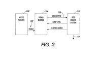
- FIG. 2 is a block diagram of a video data input system for providing data to be printed by an electrophotographic printing machine similar to the one shown in Fig. 1;
- FIG. 3 is a block diagram of the ROS driver that uses the video data from the input system of Fig. 2 to drive an ROS light source;
- FIG. 4 is a flow diagram of a process for controlling an ROS light source with a video data stream; and
- FIG. 5 is a flow diagram of a process for controlling multiple ROS light sources with multiple video data streams.
- In the drawings, like reference numerals have been used throughout to designate identical elements. FIG. 1 schematically depicts the various components of an illustrative electrophotographic printing machine incorporating an ROS control apparatus that uses a video data stream for sub-pixel generation. This ROS control apparatus is also well suited for use in a wide variety of electrostatographic printing machines and for use in ionographic printing machines. Because the various processing stations employed in the FIG. 1 printing machine are well known, they are shown schematically and their operation is described only briefly.
- FIG. 1 depicts an electrophotographic printing machine in which the ROS operation may be controlled with at least one video data stream. The machine includes a charge retentive surface in the form of an Active Matrix (AMAT)
photoreceptor belt 10 supported for movement in the direction indicated byarrow 12 so it sequentially advances through the various electrophotographic process stations. The belt is entrained about adrive roller 14,tension roller 16 and fixedroller 18. Theroller 14 is operatively connected to adrive motor 20 for moving the belt through the electrophotographic stations. - With continued reference to FIG. 1, a portion of
belt 10 passes through charging station A where a corona generating device, indicated generally by the reference numeral 22, charges the photoconductive surface ofbelt 10 to a relatively high, substantially uniform, preferably negative potential. Next, the charged portion of photoconductive surface is advanced through an imaging station B. At exposure station B, the uniformly chargedbelt 10 is exposed to a laser basedoutput scanning device 24 that causes the charge retentive surface to be selectively discharged. The laser ofdevice 24 is driven in accordance with the video data signals received fromcontroller 90. Thescanning device 24 includes a laser Raster Output Scanner (ROS) 26. - The
photoreceptor 10, which is initially charged to a voltage V0, undergoes dark decay to a level Vddp equal to about -500 volts. The areas receiving the laser output at the exposure station B are discharged to Vexpose, which is typically equal to about -50 volts. Thus, after exposure, thephotoreceptor 10 contains a monopolar voltage profile of high and low voltages, the former corresponding to charged areas and the latter corresponding to discharged or background areas. - At a first development station C, a developer housing utilizes a hybrid scavengeless development (HSD) system. The HSD system includes a development roll, better known as the donor roll, and is powered by several development fields (potentials across an air gap). The first field is the wire ac field which is used for toner cloud generation. The second field is the dc development field which is used to control the amount of developed toner mass on the photoreceptor. Other ac and dc fields between the donor, wires, and photoreceptor may be used by skilled practitioners of the art to minimize image defects and change the TRC response to the actuators. The toner cloud causes charged toner particles to be attracted to the electrostatic latent image. Appropriate developer biasing is accomplished via a power supply. This type of system is a non-contact type in which only toner particles are attracted to the latent image and there is no mechanical contact between the photoreceptor and a toner delivery device to disturb a previously developed, but unfixed, image.
- A
corona recharge device 36 having a high output current vs. control surface voltage (IN) characteristic slope is employed for raising the voltage level of both the toned and un-toned areas on the photoreceptor to a substantially uniform level. Therecharging device 36 serves to recharge the photoreceptor to a predetermined level. A second exposure orimaging device 38, which comprises a laser based output structure, such as thescanning device 24, is utilized for selectively discharging the photoreceptor on toned areas and/or bare areas, pursuant to the image to be developed with the second color developer. At this point, the photoreceptor contains toned and un-toned areas at relatively high voltage levels and toned and un-toned areas at relatively low voltage levels. These low voltage areas represent image areas which are developed using discharged area development (DAD). To this end, a negatively charged, developer material comprising color toner is employed. The toner, which by way of example, may be yellow, is contained in a developer housing structure disposed at a second developer station D and is presented to the latent images on the photoreceptor by way of a second HSD developer system. A power supply (not shown) serves to electrically bias the developer structure to a level effective to develop the discharged image areas with negatively charged yellow toner particles. - The above procedure is repeated for a third imager for a third suitable color toner such as magenta and for a fourth imager and suitable color toner such as cyan. The exposure control scheme described below may be utilized for these subsequent imaging steps. In this manner a full color composite toner image is developed on the photoreceptor belt. To the extent to which some toner charge is totally neutralized, or the polarity reversed, thereby causing the composite image developed on the photoreceptor to consist of both positive and negative toner, a negative
pre-transfer dicorotron member 50 is provided to condition the toner for effective transfer to a substrate using positive corona discharge. - Subsequent to image development a sheet of
support material 52 is moved into contact with the toner images at transfer station G. The sheet of support material is advanced to transfer station G by conventional sheet feeding apparatus, not shown. Preferably, the sheet feeding apparatus includes a feed roll contacting the uppermost sheet of a stack of copy sheets. The feed rolls rotate so as to advance the uppermost sheet from stack into a chute that directs the advancing sheet of support material into contact with photoconductive surface of thebelt 10 in a timed sequence so that the toner powder image developed thereon contacts the advancing sheet of support material at transfer station G. Transfer station G includes atransfer dicorotron 54 that sprays positive ions onto the backside ofsheet 52 to attract the negatively charged toner powder images from thebelt 10 tosheet 52. Adetack dicorotron 56 is provided for facilitating stripping of the sheets from thebelt 10. - After transfer, the sheet continues to move, in the direction of
arrow 58, onto a conveyor (not shown) which advances the sheet to fusing station H. Fusing station H includes a fuser assembly, indicated generally by thereference numeral 60, which permanently affixes the transferred powder image tosheet 52. Preferably,fuser assembly 60 comprises aheated fuser roller 62 and a backup orpressure roller 64.Sheet 52 passes betweenfuser roller 62 andbackup roller 64 with the toner powder image contactingfuser roller 62. In this manner, the toner powder images are permanently affixed tosheet 52 after it is allowed to cool. After fusing, a chute, not shown, guides the advancingsheets 52 to a catch tray, not shown, for subsequent removal from the printing machine by the operator. - After the sheet of support material is separated from the photoconductive surface of
belt 10, the residual toner particles carried by the non-image areas on the photoconductive surface are removed at cleaning station I with a cleaning brush structure contained in ahousing 66. The foregoing description is sufficient for the purposes of the present application to illustrate the general operation of a color printing machine for the purposes of describing the ROS control apparatus that uses one or more video data streams. - Referring now to FIG. 2, a
video source 100 provides video orother image data 102 to avideo buffer 104. Thevideo buffer 104 stores successive 'bytes' of video information, and providesbytes 108, one at a time in a parallel format, to anROS driver system 110 of an exposure station in an electrophotographic system. TheROS driver system 110 may be part of thecontroller 90 in FIG. 1 or a separate component. Thus, the light generated by the raster output scanner is modulated by the video bytes. The video data bytes are provided to theROS driver system 110 in response to aline sync signal 112 and a 1 X sync clock signal. Theline sync signal 112 is only active during each image line scan while the 1X clock sync is continuous. Thevideo buffer 104 only outputs video data when both the line sync and the clock are active. TheROS driver system 110 outputs adata bit stream 112 to modulate an ROS light source for purposes of exposing pixels on a latent image carried by a photoconductive belt in an electrophotographic system. - One embodiment of a
ROS driver system 110 is shown in more detail in FIG. 3. Thedriver system 110 includes a phase lockedloop 120, parallel toserial converters counter 130, and a delay and divide by eightcounter 134. The inputs of the parallel toserial converters separate video buffers 14 to receive bytes of image data, such as the video data described above. An image data byte is preferably converted to a serial bit stream with the most significant bit being first in the stream, although the byte may be converted to a bit stream in the reverse order. While the illustrated system is described with reference to eight-bit video input bytes, the principles of the illustrated system are equally applicable to any size input byte. The serial bit streams of theconverters override circuits override circuits override signal 144. Theoverride circuits - To convert the successive parallel bytes of image data into a serial data bit streams, the parallel to serial converters are synchronized with a sub-pixel clock signal that is generated by the phase locked
loop 120. In order to generate asub-pixel clock signal 148 to control the parallel to serial conversion of N-bit video bytes, areference clock signal 142 is synthesized to generate a sub-pixel clock signal having a period that is 1/N of the pixel clock period using aPLL circuit 120.PLL circuit 120 may be implemented in a known manner. For a typical eight-bit data byte application, the reference clock signal is 54 MHz and the sub-pixel clock signal is 432 MHz, although other clock rates and ratios may be used provided the sub-pixel clock rate period is less than the pixel clock signal. - The sub-pixel clock signal is provided to the parallel to
serial converters override circuits - In previously known ROS drivers, the ROS light source was turned on or off for full pixel clock periods only. With the illustrated system or one made in accordance with its principles of construction, the amount of pixel exposure may be varied in accordance with the data being image and the sub-pixels may be distributed within a pixel location. A pixel generated from a data bit stream of "11111111" enables more toner to be developed than a data bit stream of "00011100" and color may, therefore, be more accurately defined.
- As shown in Fig. 3, more than one video data byte may be provided to the
ROS driver circuit 110. The video bytes are input to separate parallel toserial converters PLL circuit 120. As a consequence, the video bit streams generated by the two parallel to serial converters are essentially in synchronization and the outputs of the override circuits likewise are essentially synchronized as a result. Therefore, the outputs of the override circuits may be used to drive separate ROS devices. Alternatively, the outputs of the override circuits may be provided to a multiplexer (not shown) so that one serial bit stream or the other may be routed to the ROS light source for modulation purposes. In this alternative embodiment, the output from the video buffers may also be controlled with the line sync and 1X clock signals to occur at different times. - An improved method for controlling an ROS light source in an electrophotographic system is shown in Fig. 4. The method includes generating a sub-pixel clock signal that has a period less than a period of a video data clock (block 200) and converting a parallel video data stream into a serial video data bit stream in synchronization with the sub-pixel clock (block 204). Preferably, the sub-pixel clock signal has a period that is 1/N of the pixel clock signal period, where N is the number of bits in a video data byte. The serial video data bit stream is used to modulate a raster output scanner (ROS) light source (block 208). The sub-pixel timing of the light source modulation provides more precise exposure control within a pixel position on a photoreceptor than available with previously known ROS driver systems. The sub-pixel clock signal generation is preferably performed with a phase lock loop circuit to help preserve synchronization between the clock signals used in the electrophotographic system.
- Another method for improved ROS light source modulation is shown in FIG. 5. This method includes generating a sub-pixel clock signal that has a period less than a period of a video data clock (block 220) and synchronously converting a first parallel video data stream and a second parallel video data stream into a first serial data bit stream and a second serial data bit stream with reference to the sub-pixel clock (block 224). Preferably, the sub-pixel clock signal has a period that is 1/N of the pixel clock signal period, where N is the number of bits in a video data byte. The data bit streams are used to synchronously modulate two ROS light sources for exposing separate color image components at an exposure station for an electrophotographic system (block 228). Alternatively, one of the first serial data bit stream and the second serial data bit stream may be selected to modulate a single ROS light source at different times to expose separate color component images on a photoconductive belt as it makes multiple passes through the electrophotographic system.
In a further embodiment the sub-pixel clock signal generation includes:
Claims (10)
- An improved ROS driver circuit comprising:a sub-pixel clock generator for generating a sub-pixel clock signal that has a period less than a period of a video data clock;a parallel to serial converter for converting a parallel video data stream into a serial video data bit stream, the parallel to serial converter being coupled to the sub-pixel clock signal for serially outputting the video data bit stream; anda raster output scanner (ROS) light source coupled to the output of the parallel to serial converter for sub-pixel control of a light signal generated by the ROS light source.
- The ROS driver circuit of claim 1, further comprising:an override circuit coupled between the serial to parallel converter and the ROS light source, the override circuit providing a constant output signal to the ROS light source in response to an override signal.
- The ROS driver circuit of claim 1 wherein the sub-pixel clock generator is a phase lock loop (PLL) circuit in which the sub-pixel clock signal is generated from a reference clock signal corresponding to the video data clock signal.
- The ROS driver circuit of claim 1 wherein the sub-pixel clock generator generates a sub-pixel clock signal having a period that is 1/N of the period of the video data clock signal, where N is the number of bits in a data byte of the parallel video data stream.
- The ROS driver circuit of claim 4 wherein a data byte of the parallel video data stream has eight bits and the sub-pixel clock is one eighth of the video data clock signal.
- The ROS driver circuit of claim 1, further comprising:a second parallel to serial converter for converting a second parallel video data stream into a second video data bit stream, the second parallel to serial converter being coupled to the sub-pixel clock signal for serially outputting the second video data bit stream.
- The ROS driver circuit of claim 6, further comprising:a second raster output scanner (ROS) light source coupled to the output of the second parallel to serial converter for sub-pixel control of a light signal generated by the second ROS light source.
- The ROS driver circuit of claim 7, further comprising:a multiplexer for selecting the serial video data bit stream of one of the first and the second parallel to serial data converter to modulate the ROS light source.
- An improved method for driving a raster output scanner comprising:generating a sub-pixel clock signal that has a period less than a period of a video data clock;converting a parallel video data stream into a serial video data bit stream,serially outputting the video data bit stream in synchronization with the sub-pixel clock; andmodulating a raster output scanner (ROS) light source with the video data bit stream for sub-pixel control of a light signal generated by the ROS light source.
- An electrophotographic system for reproducing images on media comprising:a photoconductive belt coupled by rollers to a motor for rotation of the belt in an electrophotographic system;a charging station for charging a portion of the photoconductive belt to a relatively high, substantially uniform potential;an image data buffer for receiving parallel image data;an raster output scanner (ROS) driver for converting the parallel image data to a serial image data bit stream in synchronization with a sub-pixel clock signal;an ROS light source modulated by the serial image data bit stream to generate a light directed to the charged portion of the photoconductive belt to form a latent image on the photoconductive belt corresponding to the parallel image data used to generate the serial data bit stream;a development station for developing a toner image corresponding to the latent image formed on the photoconductive belt;a transfer station for transferring the developed toner image from the photoconductive belt onto a media sheet; anda fusing station for permanently affixing the transferred toner image to the media sheet.
Applications Claiming Priority (1)
| Application Number | Priority Date | Filing Date | Title |
|---|---|---|---|
| US11/091,787 US7649544B2 (en) | 2005-03-25 | 2005-03-25 | Method and system for improved raster output scan control in an electrophotographic system |
Publications (2)
| Publication Number | Publication Date |
|---|---|
| EP1705896A2 true EP1705896A2 (en) | 2006-09-27 |
| EP1705896A3 EP1705896A3 (en) | 2008-08-20 |
Family
ID=36677970
Family Applications (1)
| Application Number | Title | Priority Date | Filing Date |
|---|---|---|---|
| EP06111695A Ceased EP1705896A3 (en) | 2005-03-25 | 2006-03-24 | Method and system for raster output scan control in an electrophotographic system |
Country Status (3)
| Country | Link |
|---|---|
| US (1) | US7649544B2 (en) |
| EP (1) | EP1705896A3 (en) |
| JP (1) | JP2006279954A (en) |
Cited By (1)
| Publication number | Priority date | Publication date | Assignee | Title |
|---|---|---|---|---|
| EP1950949A3 (en) * | 2007-01-24 | 2009-04-15 | Xerox Corporation | Sub-pixel generation for high speed color laser printers using a clamping technique for PLL (phase locked loop) circuitry |
Families Citing this family (5)
| Publication number | Priority date | Publication date | Assignee | Title |
|---|---|---|---|---|
| US7852510B2 (en) * | 2005-04-28 | 2010-12-14 | Xerox Corporation | Systems and methods for setting configuring rendering parameters for high-speed rendering devices |
| US8488186B2 (en) * | 2007-01-24 | 2013-07-16 | Xerox Corporation | Gradual charge pump technique for optimizing phase locked loop (PLL) function in sub-pixel generation for high speed laser printers switching between different speeds |
| US20080174796A1 (en) * | 2007-01-24 | 2008-07-24 | Xerox Corporation | Method of printing documents |
| JP5653010B2 (en) * | 2009-07-31 | 2015-01-14 | キヤノン株式会社 | Image forming apparatus |
| US10057523B1 (en) * | 2017-02-13 | 2018-08-21 | Alexander Krymski | Image sensors and methods with multiple phase-locked loops and serializers |
Citations (3)
| Publication number | Priority date | Publication date | Assignee | Title |
|---|---|---|---|---|
| US5737003A (en) | 1995-11-17 | 1998-04-07 | Imation Corp. | System for registration of color separation images on a photoconductor belt |
| EP1241869A2 (en) | 2001-03-14 | 2002-09-18 | Ricoh Company, Ltd. | Light-emission modulation having effective scheme of creating gray scale on image |
| US6778293B1 (en) * | 1998-12-02 | 2004-08-17 | Xerox Corporation | Fast scan image registration method and apparatus for high addressable video systems |
Family Cites Families (16)
| Publication number | Priority date | Publication date | Assignee | Title |
|---|---|---|---|---|
| JP2810365B2 (en) * | 1987-01-19 | 1998-10-15 | キヤノン株式会社 | Image forming device |
| US5091971A (en) * | 1990-09-28 | 1992-02-25 | Xerox Corporation | Method and apparatus for high-speed electronic data signal modification and improvement |
| US5291318A (en) * | 1992-11-02 | 1994-03-01 | Xerox Corporation | Holographic member for a real-time clock in a raster output scanner |
| US5381165A (en) * | 1992-11-04 | 1995-01-10 | Xerox Corporation | Raster output scanner with process direction registration |
| US5485195A (en) * | 1993-06-21 | 1996-01-16 | Xerox Corporation | Multi-phase pixel clock for a raster output scanner (ROS) printer |
| US5517230A (en) * | 1994-09-19 | 1996-05-14 | Xerox Corporation | Control system for a variable-resolution raster output scanner |
| US5606648A (en) * | 1994-12-08 | 1997-02-25 | Xerox Corporation | Apparatus and method for modulating image signals in a high addressability printing machine |
| US5764377A (en) * | 1994-12-15 | 1998-06-09 | Xerox Corporation | Video interlace system for multibeam raster output scanner |
| US5835121A (en) * | 1995-04-21 | 1998-11-10 | Xerox Corporation | Pixel exposure control for a raster output scanner in an electrophotographic printer |
| US5651017A (en) * | 1995-04-21 | 1997-07-22 | Xerox Corporation | Drive circuit for high-speed modulation of a laser diode |
| JP3261996B2 (en) * | 1996-09-20 | 2002-03-04 | 松下電器産業株式会社 | Image forming device |
| JP3606029B2 (en) * | 1998-01-13 | 2005-01-05 | 富士ゼロックス株式会社 | Image forming apparatus |
| JP2001078028A (en) * | 1999-09-06 | 2001-03-23 | Ricoh Co Ltd | Color printer |
| JP3515087B2 (en) * | 2001-09-28 | 2004-04-05 | 株式会社リコー | Pulse modulation signal generation circuit, semiconductor laser modulation device, optical scanning device, and image forming device |
| US6700594B1 (en) * | 2002-10-17 | 2004-03-02 | Xerox Corporation | Method and arrangement for registering color images |
| JP2004233717A (en) | 2003-01-31 | 2004-08-19 | Fuji Xerox Co Ltd | Image forming apparatus and image forming method |
-
2005
- 2005-03-25 US US11/091,787 patent/US7649544B2/en not_active Expired - Fee Related
-
2006
- 2006-03-20 JP JP2006075789A patent/JP2006279954A/en active Pending
- 2006-03-24 EP EP06111695A patent/EP1705896A3/en not_active Ceased
Patent Citations (3)
| Publication number | Priority date | Publication date | Assignee | Title |
|---|---|---|---|---|
| US5737003A (en) | 1995-11-17 | 1998-04-07 | Imation Corp. | System for registration of color separation images on a photoconductor belt |
| US6778293B1 (en) * | 1998-12-02 | 2004-08-17 | Xerox Corporation | Fast scan image registration method and apparatus for high addressable video systems |
| EP1241869A2 (en) | 2001-03-14 | 2002-09-18 | Ricoh Company, Ltd. | Light-emission modulation having effective scheme of creating gray scale on image |
Cited By (2)
| Publication number | Priority date | Publication date | Assignee | Title |
|---|---|---|---|---|
| EP1950949A3 (en) * | 2007-01-24 | 2009-04-15 | Xerox Corporation | Sub-pixel generation for high speed color laser printers using a clamping technique for PLL (phase locked loop) circuitry |
| US8693048B2 (en) | 2007-01-24 | 2014-04-08 | Xerox Corporation | Sub-pixel generation for high speed color laser printers using a clamping technique for PLL (phase locked loop) circuitry |
Also Published As
| Publication number | Publication date |
|---|---|
| US7649544B2 (en) | 2010-01-19 |
| EP1705896A3 (en) | 2008-08-20 |
| US20060215188A1 (en) | 2006-09-28 |
| JP2006279954A (en) | 2006-10-12 |
Similar Documents
| Publication | Publication Date | Title |
|---|---|---|
| US5049949A (en) | Extension of tri-level xerography to black plus 2 colors | |
| EP0581563B1 (en) | Pre-recharge device for voltage uniformity in read color systems | |
| US5155541A (en) | Single pass digital printer with black, white and 2-color capability | |
| US4761672A (en) | Ramped developer biases | |
| US5337136A (en) | Tandem trilevel process color printer | |
| US5241356A (en) | Method and apparatus for minimizing the voltage difference between a developed electrostatic image area and a latent electrostaic non-developed image | |
| US5221954A (en) | Single pass full color printing system using a quad-level xerographic unit | |
| EP0246457A2 (en) | Compensation for fine line prints | |
| US7649544B2 (en) | Method and system for improved raster output scan control in an electrophotographic system | |
| CA2052104C (en) | Process for coloring an electrostatic image | |
| US5210572A (en) | Toner dispensing rate adjustment using the slope of successive ird readings | |
| JPH103191A (en) | Image-on-image process color image forming method and printer for forming image-on-image process color image | |
| CA2076770C (en) | Electrostatic voltermeter (esv) zero offset adjustment | |
| JPH04338986A (en) | Printer apparatus | |
| US5089847A (en) | Highlight color copier | |
| EP0340996A2 (en) | Tri-level, highlight color imaging using ionography | |
| EP0601787B1 (en) | Colour imaging by rendering selectiv colours visible in single pass colour process | |
| US5121172A (en) | Method and apparatus for producing single pass highlight and custom color images | |
| CA2076791C (en) | Charged area (cad) image loss control in a tri-level imaging apparatus | |
| US5317373A (en) | Method and apparatus for user customized colorants in an electrophotographic printing machine | |
| US5565974A (en) | Penta-level xerographic unit | |
| US5574541A (en) | Corona dual-use for color image formation | |
| US5570194A (en) | Color image forming apparatus in which pre-transfer image exposure is performed on full color toner image on photoreceptor after fourth color toner image of Y,M,C, and BK color toner images is formed but before transferring full color toner image | |
| US7298998B1 (en) | Image registration control utilizing real time image synchronization | |
| US5223897A (en) | Tri-level imaging apparatus using different electrostatic targets for cycle up and runtime |
Legal Events
| Date | Code | Title | Description |
|---|---|---|---|
| PUAI | Public reference made under article 153(3) epc to a published international application that has entered the european phase |
Free format text: ORIGINAL CODE: 0009012 |
|
| AK | Designated contracting states |
Kind code of ref document: A2 Designated state(s): AT BE BG CH CY CZ DE DK EE ES FI FR GB GR HU IE IS IT LI LT LU LV MC NL PL PT RO SE SI SK TR |
|
| AX | Request for extension of the european patent |
Extension state: AL BA HR MK YU |
|
| PUAL | Search report despatched |
Free format text: ORIGINAL CODE: 0009013 |
|
| AK | Designated contracting states |
Kind code of ref document: A3 Designated state(s): AT BE BG CH CY CZ DE DK EE ES FI FR GB GR HU IE IS IT LI LT LU LV MC NL PL PT RO SE SI SK TR |
|
| AX | Request for extension of the european patent |
Extension state: AL BA HR MK YU |
|
| 17P | Request for examination filed |
Effective date: 20090220 |
|
| AKX | Designation fees paid |
Designated state(s): DE FR GB |
|
| 17Q | First examination report despatched |
Effective date: 20090907 |
|
| STAA | Information on the status of an ep patent application or granted ep patent |
Free format text: STATUS: THE APPLICATION HAS BEEN REFUSED |
|
| 18R | Application refused |
Effective date: 20110204 |