EP1699128A1 - Power source drive device - Google Patents
Power source drive device Download PDFInfo
- Publication number
- EP1699128A1 EP1699128A1 EP20040820643 EP04820643A EP1699128A1 EP 1699128 A1 EP1699128 A1 EP 1699128A1 EP 20040820643 EP20040820643 EP 20040820643 EP 04820643 A EP04820643 A EP 04820643A EP 1699128 A1 EP1699128 A1 EP 1699128A1
- Authority
- EP
- European Patent Office
- Prior art keywords
- soft start
- power supply
- circuit
- voltage
- terminal
- Prior art date
- Legal status (The legal status is an assumption and is not a legal conclusion. Google has not performed a legal analysis and makes no representation as to the accuracy of the status listed.)
- Withdrawn
Links
- 239000003990 capacitor Substances 0.000 claims description 98
- 230000007704 transition Effects 0.000 claims description 7
- 238000006243 chemical reaction Methods 0.000 claims description 3
- 238000010586 diagram Methods 0.000 description 12
- 238000009499 grossing Methods 0.000 description 12
- 230000009467 reduction Effects 0.000 description 5
- 238000007599 discharging Methods 0.000 description 4
- 238000011017 operating method Methods 0.000 description 4
- 230000008859 change Effects 0.000 description 1
- 230000006378 damage Effects 0.000 description 1
- 238000005516 engineering process Methods 0.000 description 1
- 238000000034 method Methods 0.000 description 1
- 230000010355 oscillation Effects 0.000 description 1
- 230000004044 response Effects 0.000 description 1
Images







Classifications
-
- H—ELECTRICITY
- H02—GENERATION; CONVERSION OR DISTRIBUTION OF ELECTRIC POWER
- H02M—APPARATUS FOR CONVERSION BETWEEN AC AND AC, BETWEEN AC AND DC, OR BETWEEN DC AND DC, AND FOR USE WITH MAINS OR SIMILAR POWER SUPPLY SYSTEMS; CONVERSION OF DC OR AC INPUT POWER INTO SURGE OUTPUT POWER; CONTROL OR REGULATION THEREOF
- H02M1/00—Details of apparatus for conversion
- H02M1/36—Means for starting or stopping converters
-
- H—ELECTRICITY
- H02—GENERATION; CONVERSION OR DISTRIBUTION OF ELECTRIC POWER
- H02M—APPARATUS FOR CONVERSION BETWEEN AC AND AC, BETWEEN AC AND DC, OR BETWEEN DC AND DC, AND FOR USE WITH MAINS OR SIMILAR POWER SUPPLY SYSTEMS; CONVERSION OF DC OR AC INPUT POWER INTO SURGE OUTPUT POWER; CONTROL OR REGULATION THEREOF
- H02M3/00—Conversion of DC power input into DC power output
- H02M3/02—Conversion of DC power input into DC power output without intermediate conversion into AC
- H02M3/04—Conversion of DC power input into DC power output without intermediate conversion into AC by static converters
- H02M3/10—Conversion of DC power input into DC power output without intermediate conversion into AC by static converters using discharge tubes with control electrode or semiconductor devices with control electrode
- H02M3/145—Conversion of DC power input into DC power output without intermediate conversion into AC by static converters using discharge tubes with control electrode or semiconductor devices with control electrode using devices of a triode or transistor type requiring continuous application of a control signal
- H02M3/155—Conversion of DC power input into DC power output without intermediate conversion into AC by static converters using discharge tubes with control electrode or semiconductor devices with control electrode using devices of a triode or transistor type requiring continuous application of a control signal using semiconductor devices only
-
- H—ELECTRICITY
- H02—GENERATION; CONVERSION OR DISTRIBUTION OF ELECTRIC POWER
- H02M—APPARATUS FOR CONVERSION BETWEEN AC AND AC, BETWEEN AC AND DC, OR BETWEEN DC AND DC, AND FOR USE WITH MAINS OR SIMILAR POWER SUPPLY SYSTEMS; CONVERSION OF DC OR AC INPUT POWER INTO SURGE OUTPUT POWER; CONTROL OR REGULATION THEREOF
- H02M3/00—Conversion of DC power input into DC power output
- H02M3/02—Conversion of DC power input into DC power output without intermediate conversion into AC
- H02M3/04—Conversion of DC power input into DC power output without intermediate conversion into AC by static converters
- H02M3/10—Conversion of DC power input into DC power output without intermediate conversion into AC by static converters using discharge tubes with control electrode or semiconductor devices with control electrode
- H02M3/145—Conversion of DC power input into DC power output without intermediate conversion into AC by static converters using discharge tubes with control electrode or semiconductor devices with control electrode using devices of a triode or transistor type requiring continuous application of a control signal
- H02M3/155—Conversion of DC power input into DC power output without intermediate conversion into AC by static converters using discharge tubes with control electrode or semiconductor devices with control electrode using devices of a triode or transistor type requiring continuous application of a control signal using semiconductor devices only
- H02M3/156—Conversion of DC power input into DC power output without intermediate conversion into AC by static converters using discharge tubes with control electrode or semiconductor devices with control electrode using devices of a triode or transistor type requiring continuous application of a control signal using semiconductor devices only with automatic control of output voltage or current, e.g. switching regulators
-
- H—ELECTRICITY
- H02—GENERATION; CONVERSION OR DISTRIBUTION OF ELECTRIC POWER
- H02M—APPARATUS FOR CONVERSION BETWEEN AC AND AC, BETWEEN AC AND DC, OR BETWEEN DC AND DC, AND FOR USE WITH MAINS OR SIMILAR POWER SUPPLY SYSTEMS; CONVERSION OF DC OR AC INPUT POWER INTO SURGE OUTPUT POWER; CONTROL OR REGULATION THEREOF
- H02M1/00—Details of apparatus for conversion
- H02M1/0003—Details of control, feedback or regulation circuits
- H02M1/0012—Control circuits using digital or numerical techniques
-
- H—ELECTRICITY
- H02—GENERATION; CONVERSION OR DISTRIBUTION OF ELECTRIC POWER
- H02M—APPARATUS FOR CONVERSION BETWEEN AC AND AC, BETWEEN AC AND DC, OR BETWEEN DC AND DC, AND FOR USE WITH MAINS OR SIMILAR POWER SUPPLY SYSTEMS; CONVERSION OF DC OR AC INPUT POWER INTO SURGE OUTPUT POWER; CONTROL OR REGULATION THEREOF
- H02M1/00—Details of apparatus for conversion
- H02M1/0003—Details of control, feedback or regulation circuits
- H02M1/0025—Arrangements for modifying reference values, feedback values or error values in the control loop of a converter
-
- H—ELECTRICITY
- H02—GENERATION; CONVERSION OR DISTRIBUTION OF ELECTRIC POWER
- H02M—APPARATUS FOR CONVERSION BETWEEN AC AND AC, BETWEEN AC AND DC, OR BETWEEN DC AND DC, AND FOR USE WITH MAINS OR SIMILAR POWER SUPPLY SYSTEMS; CONVERSION OF DC OR AC INPUT POWER INTO SURGE OUTPUT POWER; CONTROL OR REGULATION THEREOF
- H02M1/00—Details of apparatus for conversion
- H02M1/0067—Converter structures employing plural converter units, other than for parallel operation of the units on a single load
- H02M1/008—Plural converter units for generating at two or more independent and non-parallel outputs, e.g. systems with plural point of load switching regulators
Definitions
- the present invention relates to a power supply apparatus such as a switching regulator and, more particularly, to a soft start technology associated with the apparatus.
- Fig. 12 is a block diagram of a power supply apparatus according to the related art.
- the power supply apparatus is usually provided with soft start circuits 101a-101c for the purpose of preventing destruction of switching transistors due to a rush current occurring at start-up and preventing overshoot in the waveform of an output voltage as it rises.
- the soft start circuits 101a-101c are configured to gradually increase (soft start) an output voltage by increasing a conduction period (on duty) of the switching transistors over a predetermined period of time since start-up. For example, on-duty of the switching transistors is controlled so that the output voltage is increased in accordance with the waveform of the charged voltage of capacitors 104a-104c of a time-constant circuit.
- the present invention has been made in view of the aforementioned problems and relates to a power supply apparatus capable of subjecting each of a plurality of supply voltages to soft start, while preventing the number of components from being increased.
- An embodiment of the present invention provides a power supply apparatus.
- the power supply apparatus comprises: a plurality of power supply circuits which supply voltages to respective loads; a common soft start circuit which is operated when the plurality of voltages output from the plurality of power supply circuits are caused to make a transition simultaneously; an individual soft start circuit including a first terminal for outputting a predetermined fixed voltage and a second terminal outputting a voltage that varies with time, the individual soft start circuit being operated when any of the plurality of supply voltages output from the plurality of power supply circuits is caused to make a transition individually; a common soft start switch provided for each of the plurality of power supply circuits, the common soft start switch connecting the power supply circuit with the common soft start circuit; an individual soft start switch provided for each of the plurality of power supply circuits, the individual soft start switch connecting the power supply circuit with the first terminal or the second terminal of the individual soft start circuit.
- the plurality of power supply circuits subject the respective supply voltages to soft start control in accordance with the soft start voltage output from the
- the two soft start circuits are concurrently subject to soft start control at, for example, power-on or power-off.
- the individual soft start circuit is used. With this, the number of components is reduced as compared with a case where a soft start circuit is provided for each of the plurality of power supply circuits.
- the plurality of power supply circuits may close the individual soft start switch in accordance with an externally supplied control signal and apply soft start control to the respective supply voltages in accordance with the soft start voltage output from the individual soft start circuit.
- the plurality of power supply circuits may close the common soft start switch at power-on or power-off and apply soft start control to the respective supply voltages in accordance with the soft start voltage output from the common soft start circuit.
- the common soft start circuit may comprise: a constant current source which charges a common soft start capacitor by supplying a constant current thereto; and a transistor which is provided parallel with the common soft start capacitor and discharges the common soft start capacitor in accordance with a timing signal input to the gate of the transistor.
- the individual soft start circuit may comprises: a latch power supply which outputs a predetermined voltage; and a digital-to-analog conversion circuit which outputs a voltage of a ramp waveform in accordance with a digital signal input to a digital input terminal, the output voltage at its maximum level being equal to the predetermined voltage, wherein the predetermined voltage may be output from a first terminal and the voltage with a ramp waveform may be output from a second terminal.
- the individual soft start circuit may comprise: a latch power supply which outputs a predetermined voltage; an individual soft start capacitor; a constant current source which charges the individual soft start capacitor by supplying a constant current thereto; and a transistor which is provided parallel with the individual soft start capacitor and discharges the individual soft start capacitor in accordance with a timing signal input to the gate of the transistor, wherein the predetermined voltage may be output from a first terminal and a voltage at a node between the individual soft start capacitor and the constant current source may be output from a second terminal.
- the individual soft start circuit may comprise: a latch power supply which outputs a predetermined voltage; an individual soft start capacitor; a constant current source which charges the individual soft start capacitor by supplying a constant current thereto; and a transistor which is provided parallel with the individual soft start capacitor and discharges the individual soft start capacitor in accordance with a timing signal input to the gate of the transistor, wherein the predetermined voltage may be output from a first terminal and a voltage at a node between the individual soft start capacitor and the constant current source may be output from a second terminal.
- the individual soft start circuit may comprise: a latch power supply which outputs a predetermined voltage; an individual soft start capacitor; a charge transistor provided between the individual soft start capacitor and the latch power supply; and a discharge transistor which is provided parallel with the individual soft start capacitor and discharges the individual soft start capacitor in accordance with a timing signal input to the gate of the discharge transistor, wherein the predetermined voltage may be output from a first terminal and a voltage at a node between the individual soft start capacitor and the discharge transistor may be output from a second terminal.
- Fig. 1 and Fig. 3 are block diagrams of a power supply apparatus according to an embodiment of the present invention.
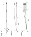
- Figs. 2A through 2C are time charts indicating voltage variation at respective nodes at power-on.
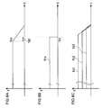
- Figs. 4A through 4C are time charts indicating voltage variation at respective nodes occurring when a power supply circuit 105b is turned off.
- Figs. 5A through 5C are time charts indicating voltage variation at respective nodes occurring when the power supply circuit 105b in an off state shifts to an on state.
- Figs. 6A through 6C are time charts showing voltage variation at respective nodes occurring at power-off.
- Fig. 1 and Fig. 3 are block diagrams of a power supply apparatus according to an embodiment of the present invention.
- Figs. 2A through 2C are time charts indicating voltage variation at respective nodes at power-on.
- Figs. 4A through 4C are time charts indicating voltage variation at respective nodes occurring when a power supply circuit 105b is turned off.
- FIG. 7 is a circuit diagram of a power supply circuit according to the embodiment of the present invention.
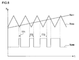
- Fig. 8 illustrates time waveforms indicating the operation of the circuit.
- Fig. 9 illustrates an example of circuit structure of a common soft start circuit 103 and a common soft start capacitor 104 according to the embodiment of the present invention.
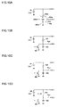
- Figs. 10A through 10D are circuit diagrams of individual soft start circuits according to the embodiment of the present invention.
- Figs. 11A through 11I are time charts indicating signal waveforms and voltage variation occurring in the power supply apparatus.
- Fig. 1 is a block diagram illustrating the structure of a power supply apparatus 1000 according to the embodiment of the present invention.
- the power supply apparatus 1000 is provided with three power supply circuits 105a-105c which output supply voltages Vo1-Vo3 to different loads 117a-117c, respectively.
- the power supply voltage for the apparatus as a whole is Vcc(V).
- Vcc(V) When power derived from the power supply voltage Vcc is turned on, the supply voltages Vo1-Vo3(V) are output to the loads 117a-117c, respectively.
- the power supply apparatus 1000 includes a voltage reduction reset circuit 113, an individual soft start circuit 101, a common soft start circuit 103, a common soft start capacitor 104, power supply circuits 105a-105c, coils 107a-107c, smoothing capacitors 109a-109c and switches SW.
- the power supply circuit 105a is connected to the load 117a via the coil 107a.
- the power supply circuit 105b and the power supply circuit 105c are connected to the load 117b and the load 117c, respectively, via the coil 107b and the coil 107c, respectively.
- An end of the smoothing capacitor 109a for smoothing the voltage Vo1 supplied to the load 117a is connected to a node between the coil 107a and the load 117a. The other end of the smoothing capacitor 109a is grounded.
- an end of the smoothing capacitor 109b for generating the voltage Vo2 supplied to the load 117b is connected to a node between the coil 107b and the load 117b. The other end of the smoothing capacitor 109b is grounded.
- an end of the smoothing capacitor 109c for generating the voltage Vo3 supplied to the load 117c is connected to a node between the coil 107c and the load 117c. The other end of the smoothing capacitor 109c is grounded.
- Each of the power supply circuits 105a-105c is connected to the individual soft start circuit 101 and the common soft start circuit 103.
- the power supply circuit 105a is connected to switches SW1a-SW3a. By selectively closing the switches SW1a-SW3a, the power supply circuit 105a is connected to a first terminal 1011 of the individual soft start circuit 101, a second terminal 1013 of the individual soft start circuit 101 or an output terminal 1014 of the common soft start circuit 103.
- the power supply circuit 105b is connected to switches SW1b, SW2b and SW3b. By selectively closing the switches SW1b, SW2b and SW3b, the power supply circuit 105b is connected to the first terminal 1011 of the individual soft start circuit 101, the second terminal 1013 of the individual soft start circuit 101 or the output terminal 1014 of the common soft start circuit 103.
- the power supply circuit 105c is connected to switches SW1c-SW3c. By selectively closing the switches SW1c-SW3c, the power supply circuit 105c is connected to the first terminal 1011 of the individual soft start circuit 10, the second terminal 1013 of the individual soft start circuit 101 or the output terminal 1014 of the common soft start circuit 103.
- the soft start voltage from one of the three systems is switchably input to each of the power supply circuits 105a-105c. Details will be described later.
- the switches SW1a-SW1c are common soft start switches for connecting the power supply circuits 105a-105c to the common soft start circuit 103.
- the switches SW3a-SW3c are individual soft start switches that are closed when the individual soft start circuit 101 is started so as to connect the power supply circuits 105a-105c to the second terminal 1013 of the individual soft start circuit 101.
- the switches SW2a-SW2c are connected to the first terminal 1011 of the individual soft start circuit 101 and are individual soft start switches for fixing the soft start voltage when it has risen.
- these switches SW1a-SW1c, SW2a-SW2c and SW3a-SW3c will be referred to as switches SW where distinction thereof is not essential.
- the common soft start capacitor 104 is a time-constant circuit used in performing common soft start described later.
- the voltage reduction reset circuit 113 is a circuit for transmitting a reset signal Vrs to the power supply circuits 105a-105c.
- the reset signal Vrs is switched to a high level or a low level.
- the high level of the reset signal corresponds to a steady state and the low level corresponds to a reset state.
- the host 111 transmits control signals Vcnt1-Vcnt3 described later to the power supply circuits 105a-105c so as to control the power supply circuits 105a-105c and exchanges control signals and information signals with various apparatuses (not shown).
- control signals Vcnt1-Vcnt3 transmitted from the host 111 to the power supply circuits 105a-105c are illustrated using a single signal line. Actually, a plurality of controls signals are transmitted.
- the specific circuit structure of the individual soft start circuit 101 and the common soft start circuit 103 will be described later (Fig. 9 and Figs. 10A-10D).
- the host 111 controls on and off of the switches SW at power-on.
- the switches SW1a-SW1c are closed as illustrated in Fig. 1 and the other switches are open so as to connect soft start terminals 720a-720c of the power supply circuits 105a-105c to the common soft start circuit 103 and the common soft start capacitor 104.
- the power supply circuits 105a-105c are soft started by the common soft start circuit 103 and the common soft start capacitor 104.
- Figs. 2A through 2C are time charts showing voltage variation at respective nodes occurring at power-on.
- Fig. 2A illustrates the variation of the power supply voltage Vcc.
- Fig. 2B illustrates the variation of a common soft start voltage Vsse of the common soft start circuit 103.
- Fig. 2C illustrates the variation of the voltages Vo1-Vo3 supplied to the loads 117a-117c.
- the rise time of the power supply voltage Vcc is T20 (msec). An overshoot is caused without the soft start circuit.
- the rise time of the common soft start voltage Vsse of the common soft start capacitor 104 is T21 (msec).
- Fig. 2C illustrates the variation of the voltages Vo1-Vo3 (V) supplied to the loads 117a-117c when soft start is performed by using the common soft start circuit 103 and the common soft start capacitor 104.
- the rise time of the supply voltages (Vo1-Vo3) is T22 (msec).
- the switches SW1a, SW1b and SW1c are closed so that the power supply circuits 105a-105c are gradually started by the common soft start voltage Vsse output from the common soft start circuit 103.
- power saving is achieved by turning the plurality of power supply circuits 105a-105c on and off individually in accordance with the operating condition of the loads 117a-117c.
- the host 111 transmits the control signals Vcntl-Vcnt3 for individually controlling the on and off state of the power supply circuits 105a-105c.
- the high level of the control signals Vcnt1-Vcnt3 corresponds to an on state and the low level corresponds to an off state.
- Fig. 3 is a block diagram illustrating the structure of the power supply apparatus 1000 according to the embodiment of the present invention.
- the reset signal Vrs output from the voltage reduction reset circuit 113 is at a high level.
- the control signal Vcnt2 transmitted from the host 111 designates a shift of the power supply circuit 105b to an off state while the reset signal Vrs remains at a high level, the switches SW1b-SW3b connected to the soft start terminal 720b of the power supply circuit 105b are all opened.
- Figs. 4A through 4C are time charts indicating voltage variation at respective nodes occurring when the power supply circuit 105b is turned off.
- Fig. 4A illustrates the variation of the control signal Vcnt2 transmitted from the host 111 to the power supply circuit 105b (the high level corresponds to an off state and the low level corresponds to an on state).
- Fig. 4B illustrates the variation of the voltage supplied to the load 117b.
- Fig. 4C illustrates the variation of the voltages supplied to the load 117a and the load 117c.
- the vertical axis represents a voltage (V) and the horizontal axis represents time t (msec).
- the host control signal Vcnt2 transmitted from the host 111 to the power supply circuit 105b is switched from a low level to a high level at time T40, designating a shift to an off state.
- the power supply circuit 105b receiving the instruction to shift to an off state from the host 111 suspends its voltage step-down operation. As a result, the voltage Vo2 supplied to the load 117b is dropped starting at time T40. Voltage supply to the load 117b is eventually suspended.
- Fig. 4C illustrates the (constant) voltages Vo1 and Vo13 supplied to the load 117a and the load 11c, respectively.
- the operation of the plurality of power supply circuits 105a-105c is individually turned on or off in accordance with the operating conditions of the loads 117a-117c. Accordingly, in order to restart the power supply circuit 105 after turning it off, the control signal Vcnt transmitted from the host 111 to the power supply circuit 105 is switched to a low level.
- the control signal Vcnt transmitted from the host 111 to the power supply circuit 105 is switched to a low level.
- the power supply circuit 105b directed by the host 111 to shift to an on state closes only the switch SW3b (indicated by a broken line 301 in Fig. 3) and maintains the switches SW1b and the switch SW2b open. With this, the power supply circuit 105b connects its soft start terminal 720b to the individual soft start circuit 101 via the second terminal 1013. Accordingly, the power supply circuit 105b is soft started at restart by a soft start voltage Vssi output from the individual soft start circuit 101.
- Figs. 5A through 5C are time charts indicating voltage variation at respective nodes when the power supply circuit 105b in an off state shifts to an on state.
- Fig. 5A illustrates voltage variation of the control signal Vcnt2 transmitted from the host 111 to the power supply circuit 105b (the high level corresponds to off and the low level corresponds to on).
- Fig. 5B illustrates the variation of the individual soft start voltage Vssi output from the individual soft start circuit 101.
- Fig. 5C illustrates the variation of the voltage Vo2 supplied to the load 117b.
- the vertical axis represents a voltage (V) and the horizontal axis represents time t (msec).
- the control signal Vcnt2 transmitted from the host 111 to the power supply circuit 105b shifts from a high level to a low level at time T50, designating a shift to an on state.
- the individual soft start voltage Vssi output from the second terminal 1013 of the individual soft start circuit 101 rises to a maximum voltage VH in a period T51 (msec).
- Fig. 5C illustrates the variation of the voltage Vo2(V) supplied to the load 117b occurring when soft start is performed using the invidual soft start circuit 101.
- the rise time of the supply voltage (Vo2) is T52(msec).
- the power supply circuit 105b opens the switch SW3b and closes the switch SW2b in a period after time T53, when the individual soft start voltage Vssi output from the second terminal 1013 of the individual soft start circuit 101 fully rises. Details will be described later.
- the soft start terminal 720b of the power supply circuit 105b is connected to the first terminal 1011 of the individual soft start circuit 101.
- the soft start terminal 720b is fixed at the maximum voltage VH output from the first terminal 1011 of the individual soft start circuit 101.
- the reset signal Vrs output from the voltage reduction reset circuit 113 to the power supply circuits 105a-105c is brought to a low level.
- the power supply circuits 105a-105c switch their destination of connection from the individual soft start circuit 101 to the common soft start circuit 103 and the common soft start capacitor 104.
- the power supply circuits 105a-105c close the switches SW1a-SW1c, respectively, and open the switches SW2a, SW3a, SW2b, SW3b, SW2c and SW3c so as to connect the soft start terminals 720a-720c of the power supply circuits 105a-105c to the common soft start circuit 103 and the common soft start capacitor 104.
- Figs. 6A through 6C are time charts showing voltage variation at respective nodes occurring at power-off.
- Fig. 6A illustrates the variation of the power supply voltage Vcc.
- Fig. 6B illustrates voltage variation of the reset signal Vrs (the high level corresponds to a steady state and the low level corresponds to a reset state).
- Fig. 6C illustrates the variation of the voltage supplied to the loads 117a-117c.
- the vertical axis represents a voltage (V) and the horizontal axis represents time t (msec).
- the power supply voltage Vcc starts to drop at time T60.
- the reset signal Vrs transmitted from the voltage reduction reset circuit 113 to the power supply circuits 105a-105c is brought to a low level.
- the reset signal Vrs goes low, designating a shift to a reset state, the voltages Vo1-Vo3 supplied to the loads 117a-117c drop as illustrated in Fig. 6C.
- Fig. 7 illustrates an example of circuit structure of the power supply circuit 105 according to the embodiment of the present invention.
- the following description concerns the structure of the power supply circuit 105b. The description applies similarly to the power supply circuit 105a and the power supply circuit 105c.
- Fig. 7 also illustrates the coil 107b and the smoothing capacitor 109b connected to the power supply circuit 105b.
- the power supply circuit 105b includes an error amplifier 709, an oscillator 701, a driver 705, a switching transistor 703, a diode 713, a PWM comparator 707, resistors R1 and R2, and a feedback resistor 711.
- the soft start terminal 720b is a terminal for connection with the switches SW1b-SW3b.
- the soft start voltage Vss output from the individual soft start circuit 101 or the common soft start circuit 103 is input to the terminal.
- the power supply voltage Vcc is applied to the input voltage terminal 730.
- the voltage Vo2 supplied to the load is fed back to a feedback terminal 740.
- the switching transistor 703, the diode 713 and the externally coupled coil 107 and the smoothing capacitor 109b constitute a switching regulator of a step-down type.
- the switching regulator steps down the power supply voltage Vcc input to the input voltage terminal 730 to a target value determined by a reference voltage Vref and outputs the stepped-down voltage.
- the power supply voltage Vcc an input voltage
- the other end of the switching transistor 703 is connected to the rectifying diode 713.
- the voltage at a node between the switching transistor 703 and the diode 713 is output as the supply voltage Vo2 via the coil 107b.
- a pulse-width modulated switching signal output from the driver 705 is input to the gate of the switching transistor 703.
- the switching transistor 703 is subject to on and off control in accordance with the duty ratio of the switching signal.
- the coil 107b is supplied with a current alternately via the switching transistor 703 and the diode 713, in accordance with the on and off of the switching transistor 703.
- the coil 107b and the smoothing capacitor 109b constitute a filter and the supply voltage Vo2 is output as a smoothed dc voltage.
- the supply voltage Vo2 is divided by the resistors R1 and R2 before being fed to the error amplifier 709.
- the error amplifier 709 amplifies a voltage error of the supply voltage Vo2 divided by the resistors R1 and R2 with respect to the soft start voltage Vss applied to the soft start terminal 720 and a voltage error of the supply voltage Vo2 divided by the resistors with respect to the reference voltage Vref.
- the error amplifier 709 outputs the error voltage Verr to the PWM comparator 707.
- the feedback resistor 711 is connected to the error amplifier 709.
- the oscillator 701 outputs a triangular wave at a predetermined frequency that defines a switching period.
- the resistor 715a and the capacitor 715b are provided to adjust the oscillating frequency of the oscillator 701.
- the PWM comparator 707 compares the error voltage Verr output from the error amplifier 709 with the oscillating voltage Vosc output from the oscillator 701. If Verr>Vosc, the PWM comparator 707 generates a high-level pulse-width modulated PWM signal Vpwm. If Verr ⁇ Vosc, a low-level PWM signal Vpwm is output.
- the driver 705 controls the gate voltage of the switching transistor 703 in accordance with the PWM signal Vpwm generated by the PWM comparator 707 so as to turn on or off the switching transistor 703.
- the power supply circuit 105b maintains the voltage Vo2 supplied to the load 117b according to the PWM scheme for controlling the on-time ratio (the ratio between the conduction time of the switching transistor 703 and the oscillation period of the oscillator 701) of the switching transistor 703 (a main switching element) by a gate drive pulse.
- the on-time ratio is determined by comparing the output voltage Vosc of the oscillator 701, which is a voltage input to the inverting input of the PWM comparator 707, with the error voltage Verr output from the error amplifier 709, which is a voltage input to the non-inverting input of the PWM comparator 707.
- the soft start function is achieved by gradually increasing the on-time ratio by progressively extending a duration in which the error voltage Verr is higher than the output voltage Vosc of the oscillator 701 (interval T71 -> interval T72 -> interval T73) as illustrated in Fig. 8.
- the soft terminal 720 is connected to the switches SW1b, SW2b and SW3b according to this embodiment, one of “the common soft start circuit 103 and the common soft start capacitor 104" and “the individual soft start circuit 101" is connected to the non-inverting input of the error amplifier 709, by selectively closing the switches SW1b, SW2b and SW3b.
- the common soft start circuit 103 and the common soft start capacitor 104" are connected to the non-inverting input of the error amplifier 709 at power-on. Therefore, the common soft start voltage Vsse is input to the non-inverting input as the soft start voltage Vss.
- the feedback voltage Verr of Fig. 8 is gradually increased with the common soft start Voltage Vsse.
- the individual soft start circuit 101 is connected to the non-inverting input of the error amplifier 709 when the power supply circuit 105b shifts from an off state to an on state. Accordingly, the individual soft start voltage Vssi output from the individual soft start circuit 101 is input to the non-inverting input of the error amplifier 709 as the soft start voltage Vss.
- the error voltage Verr of Fig. 8 is increased with the individual soft start voltage Vssi.
- Fig. 9 illustrates an example of circuit structure of the common soft start circuit 103 and the common soft start capacitor 104 according to the embodiment.
- An end of the common soft start capacitor 104 is grounded. The other end thereof is connected to a node C1 between the common soft start circuit 103 and the switches SW1a, SW1b and SW1c.
- a constant current source 801 is for charging the common soft start capacitor 104.
- the constant current source 801 is connected to the power supply Vcc.
- a node between the constant current source 801 and an end of a resistor 805 is connected to the common soft start capacitor 104.
- the other end of the resistor 805 is connected to the drain of a transistor 803.
- the source of the transistor 803 is grounded.
- the gate of the transistor 803 is connected to an electronic control circuit (not shown) and receives an timing signal.
- the transistor 803 is turned on or off in accordance with the timing signal input to the gate of the transistor 803.
- the common soft start capacitor 104 is discharged so that the voltage at the output terminal 1014 drops to a level close to the ground potential.
- the transistor 803 is turned off, the potential at the output terminal 1014 is increased as a result of a charge Q being stored in the common soft start capacitor 104 at power-on by a constant current supplied from the constant current source 801.
- the resistor 805 of the common soft start circuit 103 illustrated in Fig. 9 is not essentially. While the transistor 803 is illustrated in Fig. 9 as a MOS transistor, a bipolar transistor may also be used.
- Figs. 10A-10D illustrate circuit structures of the individual soft start circuit 101 according to the embodiment.
- a first terminal 1011 and a second terminal 1013 there are provided a first terminal 1011 and a second terminal 1013.
- the individual soft start voltage Vssi that is gradually increased with time is output from the second terminal 1013.
- the maximum value VH of the individual soft start voltage Vssi is constantly output from the first terminal 1011.
- a DAC circuit 900 is provided with a digital input terminal 909a, an analog output terminal 904a, a maximum voltage terminal 903a and a minimum voltage terminal 905a.
- the maximum voltage terminal 903a is connected to a latch power supply 910 so that the voltage VH is applied to the maximum voltage terminal 903a.
- the minimum voltage terminal 905a is grounded.
- the digital input terminal 909a is connected to a timing generation circuit (not shown). The timing generation circuit is controlled by a control signal from the host 111.
- the first terminal 1011 outputs the maximum voltage VH output from the latch power supply 910.
- the analog output terminal 904a outputs a voltage with a ramp waveform with a minimum voltage VL, which is applied to the minimum voltage terminal 905a, and a maximum voltage VH, which is applied to the maximum voltage terminal 903a.
- the voltage output from the analog output terminal 904a is output from the second terminal 1013.
- the potential at the second terminal 1013 is increased in accordance with an increase in digital code input to the digital input terminal 909a.
- the power supply circuits 105a-105c connect themselves with the latch power supply 910 by closing the switch SW2a (or SW2b, SW2c) and opening the switch SW3a (or SW3b, SW3c).
- the soft start voltages Vss1-Vss3 input to the respective soft start terminals 720a-720c can be fixed.
- the first terminal 1011 outputs the voltage VH output from the latch power supply 910.
- An end of an individual soft start capacitor 920 is grounded and the other end thereof is connected to a constant current source 922.
- the voltage at a node between the capacitor 920 and the source 922 is output from the second terminal 1013.
- the constant current source 922 charges the individual soft start capacitor 920.
- a node between the constant current source 922 and the individual soft start capacitor 920 is connected to the collector of a transistor 902.
- the emitter of the transistor 902 is grounded.
- the base of the transistor 902 is connected to a timing generation circuit (not shown). The timing generation circuit is driven by a control signal from the host 111.
- the transistor 902 when the control signal Vcnt transmitted from the host 111 designates a shift to an on state, the transistor 902 is turned off, causing the individual soft start capacitor 920 to be charged by the constant current supplied from the constant current source 922. As a result, the potential at the second terminal 1013 is increased.
- the power supply circuits 105a-105c connect themselves with the latch power supply 910 by closing the switch SW2a (or SW2b, SW2c) and opening the switch SW3a (or SW3b, SW3c). With this, the soft start voltages Vss1-Vss3 input to the respective soft start terminals 720a-720c can be fixed.
- the structure of the individual soft start circuit 101 of Fig. 10C is such that the constant current source 922 of Fig. 10B is replaced by a resistor 924.
- the first terminal 1011 outputs the voltage VH output from the latch power supply 910.
- a node between the resistor 924 and the latch power supply 910 is connected to the first terminal 1011.
- a node between the resistor 924 and the individual soft start capacitor 920 is connected to the collector of the transistor 902.
- the emitter of the transistor 902 is grounded.
- the base of the transistor 902 is connected to a timing generation circuit (not shown). The timing generation circuit is driven by a control signal from the host 111.
- the transistor 902 when the control signal Vcnt transmitted from the host 111 designates a shift to an on state, the transistor 902 is turned off, causing the individual soft start capacitor 920 to be charged. As a result, the potential at the second terminal 1013 is increased in accordance with a time constant determined by the resistance of the resistor 924 and the capacitance of the individual soft start capacitor 920.
- the power supply circuits 105a-105c connect themselves with the latch power supply 910 by closing the switch SW2a (or SW2b, SW2c) and opening the switch SW3a (or SW3b, SW3c). With this, the soft start voltages Vss1-Vss3 input to the respective soft start terminals 720a-720c can be fixed.
- the structure of the individual soft start circuit 101 of Fig. 10D is such that the constant current source 922 of Fig. 10B is replaced by a transistor 926.
- the first terminal 1011 outputs the voltage VH output from the latch power supply 910.
- An end of the individual soft start capacitor 920 is grounded and the other end thereof is connected to the second terminal 1013.
- the gate of the transistor 926 is connected to a timing generation circuit (not shown).
- the timing generation circuit transmits a PWM signal in accordance with a control signal from the host 111 so as to change the conduction time of the transistor 926. As the conduction time varies, the transistor 926 functions as a variable resistor.
- a node between the drain of the transistor 926 and the latch power supply 910 is connected to the first terminal 1011.
- a node between the source of the transistor 926 and the individual soft start terminal 920 is connected to the collector of the transistor 902 and the second terminal 1013.
- the emitter of the transistor 902 is grounded.
- the base of the transistor 902 is connected to a timing generation circuit (not shown). The timing generation circuit is driven by a control signal from the host 111.
- the transistor 902 when the control signal Vcnt transmitted from the host 111 designates a shift to an on state, the transistor 902 is turned off, causing the individual soft start capacitor 920 to be charged. As a result, the potential at the second terminal 1013 is increased.
- the power supply circuits 105a-105c connect themselves with the latch power supply 910 by closing the switch SW2a (or SW2b, SW2c) and opening the switch SW3a (or SW3b, SW3c). With this, the soft start voltages Vss1-Vss3 input to the respective soft start terminals 720a-720c can be fixed. While the transistor 902 is illustrated in Figs. 10A, 10B and 10C as a bipolar transistor, a MOS transistor may also be used.
- Figs. 11A through 11I are time charts showing signal waveforms and voltage variation occurring when the control signal is transmitted from the host. The following description with reference to Figs. 11A-11I relates to a case where the DAC circuit of Fig. 10A is used in the individual soft start circuit 101.
- Fig. 11A shows a waveform of the control signal Vcnt1 supplied to the power supply circuit 105a.
- the high level corresponds to an off signal and the low level corresponds to an on signal.
- Fig. 11B shows the waveform of the control signal Vcnt2 supplied to the power supply circuit 105b.
- the high level corresponds to an off signal and the low level corresponds to an on signal.
- Fig. 11C shows the waveform of the output voltage from the DAC circuit 900, i.e., the individual soft start voltage Vssi output from the second terminal 1013 of the individual soft start circuit 101.
- Figs. 11D-11G show the waveforms indicating the open and closed conditions of the switch SW3a, the switch SW2a, the switch SW3b and the switch SW2b, respectively.
- the high level corresponds to a closed state and the low level corresponds to an open state.
- Fig. 11H shows the waveform of the soft start voltage Vss1 input to the soft start terminal 720a of the power supply circuit 105a.
- Fig. 11I shows the waveform of the soft start voltage Vss2 input to the soft start terminal 720b of the power supply circuit 105b.
- the power supply circuit 105a receiving the control signal Vcnt1 at a low level from the host 111, opens the switch SW1a and the switch SW2a and closes the switch SW3a so as to connect itself to the second terminal 1013 of the individual soft start circuit 101. Accordingly, the soft start voltage Vss1 input to the soft start terminal 720a of the power supply circuit 105a is increased (Fig. 11H) as the individual soft start voltage Vssi output from the DAC circuit 900 is increased (Fig. 11C).
- the output voltage from the DAC circuit 900 (Fig. 11C) reaches the maximum value VH at time T103, triggering the power supply circuit 105a to close the switch SW2a. Thereafter, the switch SW2a and the switch SW3a are both closed until time T105. This is to prevent the voltage output from the individual soft start circuit 101 from becoming intermittent. In this state, the switch SW1a is open. In this period, the individual soft start circuit 101 and the power supply circuit 105a are connected to each other via the first terminal 1011 and the second terminal 1013. As illustrated in Fig. 11H, the soft start voltage Vss1 input to the soft start terminal 720a is maintained at the maximum value VH.
- the power supply circuit 105a opens the switch SW3a. Thereafter, only the switch SW2a is closed until the control signal Vcnt1 makes a transition from a low level to a high level. Accordingly, the individual soft start circuit 101 and the power supply circuit 105a are connected to each other via the first terminal 1011 after time T105 and until the control signal Vcnt1 makes a transition to a high level. As illustrated in Fig. 11H, the soft start voltage Vss1 input to the soft start terminal 720 is maintained at the maximum value VH.
- the power supply circuit 105b opens the switch SW1b and the switch SW2b and closes the switch SW3b so as to connect itself to the second terminal 1013 of the individual soft start circuit 101. Accordingly, as the individual soft start voltage Vssi output from the DAC circuit 900 is increased (Fig. 11C), the soft start voltage Vss2 input to the soft start terminal 720b of the power supply circuit 105b is increased (Fig. 111).
- the soft start voltage Vssi reaches the maximum value VH at time T109, triggering the power supply circuit 105b to close the switch SW2b. Thereafter, the switch SW2b and the switch SW3b are both closed until time T111. This is to prevent the voltage output from the individual soft start circuit 101 from becoming intermittent. In this state, the switch SW1b is open. In this period, the individual soft start circuit 101 and the power supply circuit 105a are connected to each other via the first terminal 1011 and the second terminal 1013. As illustrated in Fig. 11H, the soft start voltage Vss2 input to the soft start terminal 720b is maintained at the maximum value VH.
- the power supply circuit 105b opens the switch SW3b. Thereafter, only the switch SW2b is closed until time T113. Accordingly, the individual soft start circuit 101 and the power supply circuit 105b are connected to each other via the first terminal 1011 in a period between T111 and T113.
- the soft start voltage Vss2 input to the soft start terminal 720b is maintained at the maximum value VH.
- the control signal Vcnt2 makes a transition to a high level at time T113, triggering the power supply circuit 105b to open the switch SW2b again. In this state, the switches SW1b-SW3b connected to the power supply circuit 105b are all opened so that the soft start voltage Vss2 input to the soft start terminal 720 converges to 0V.
- circuit illustrated in Fig. 7 is used as the power supply circuit and the circuit illustrated in Fig. 9 is used as the common soft start circuit, alternative circuit structures are possible.
- the power supply circuit of the embodiment is described as being implemented by a switching regulator of a step-down type, a switching regulator of a step-up type may also be used.
- the power supply apparatus comprises: a plurality of power supply circuits which supply voltages to respective loads; a common soft start switch connected to each of the plurality of power supply circuits; an individual soft start switch connected to each of the plurality of power supply circuits; a common soft start circuit commonly connected to the plurality of power supply circuits via the common soft start switch; and an individual soft start circuit commonly connected to the plurality of power supply circuits via the individual soft start switch.
- the power supply circuit may connect itself to the individual soft start circuit in response to a control signal, by closing the individual soft start switch connected to the circuit.
- the power supply circuit may connect itself to the common soft start circuit and the common soft start capacitor at power-off, by closing the common soft start switch connected to the circuit.
- the common soft start circuit preferably comprises: a constant current source for charging the common soft start capacitor via a node connected to the common soft start capacitor; and a transistor for discharging the common soft start capacitor via the node in accordance with a timing signal input to the transistor gate.
- the individual soft start circuit preferably comprises: first and second nodes connected to the individual soft start switch; a DAC circuit for outputting a voltage of a ramp waveform via the first node; and a latch power supply for outputting a predetermined voltage via the second node.
- the individual soft start circuit in one variation preferably comprises: first and second nodes connected to the individual soft start switch; an individual soft start capacitor; a constant current source for charging the individual soft start capacitor; a second transistor for discharging the individual soft start capacitor via a node between the individual soft start capacitor and the constant current source and via the first node, in accordance with a timing signal input to the transistor gate; and a latch power supply for outputting a constant voltage via the second node.
- the individual soft start circuit in another variation preferably comprises: first and second nodes connected to the individual soft start switch; an individual soft start capacitor; a resistor for charging the individual soft start capacitor; a second transistor for discharging the individual soft start capacitor via a node between the individual soft start capacitor and the resistor and via the first node, in accordance with a timing signal input to the transistor gate; and a latch power supply for outputting a constant voltage via the second node.
- the individual soft start circuit in another variation preferably comprises: first and second nodes connected to the individual soft start switch; an individual soft start capacitor; a first transistor for charging the individual soft start capacitor; a second transistor for discharging the individual soft start capacitor via a node between the individual soft start capacitor and the first transistor and via the first node, in accordance with a timing signal input to the transistor gate; and a latch power supply for outputting a constant voltage via the second node.
- the apparatus according to the present invention can be used to drive a variety of loads.
Landscapes
- Engineering & Computer Science (AREA)
- Power Engineering (AREA)
- Dc-Dc Converters (AREA)
Abstract
A power source drive device includes a plurality of power source drive circuits, a switch SW connected to the respective power source drive circuits, a common soft start circuit commonly connected to the power source drive circuits via the switch SW, and an individual soft start circuit. When power supply is turned on or off, the power source drive circuit is commonly connected to the common soft start circuit.
Description
- The present invention relates to a power supply apparatus such as a switching regulator and, more particularly, to a soft start technology associated with the apparatus.
- Fig. 12 is a block diagram of a power supply apparatus according to the related art. As illustrated, the power supply apparatus is usually provided with
soft start circuits 101a-101c for the purpose of preventing destruction of switching transistors due to a rush current occurring at start-up and preventing overshoot in the waveform of an output voltage as it rises.
Thesoft start circuits 101a-101c are configured to gradually increase (soft start) an output voltage by increasing a conduction period (on duty) of the switching transistors over a predetermined period of time since start-up. For example, on-duty of the switching transistors is controlled so that the output voltage is increased in accordance with the waveform of the charged voltage ofcapacitors 104a-104c of a time-constant circuit. - However, when a plurality of loads (117a-117c) requiring different supply voltages (Vo1-Vo3) are provided in a single apparatus, there may arise a need to provide a plurality of
power supply circuits 105a-105c in the apparatus.
In this case, the power supply apparatus is often subject to on and off control by ahost 111 after a sufficient period of time has elapsed since power from a power supply voltage Vcc indicated in the drawing is turned on (hereinafter, referred to as power-on), for the purpose of power saving. Accordingly, such a multi-channel power supply apparatus needs thesoft start circuits 101a-101c and theexternal capacitors 104a-104c for respective channels, thwarting efforts reduce the number of components. - "Example of applied circuits" section in non-patent document 1 describes "capacitors SS1, SS2, SS3" which correspond to the external capacitors described above.
[non-patent document]
Manual of "HDD system power supply BD9786KN", January 2003, Rohm Corporation - The present invention has been made in view of the aforementioned problems and relates to a power supply apparatus capable of subjecting each of a plurality of supply voltages to soft start, while preventing the number of components from being increased.
- An embodiment of the present invention provides a power supply apparatus. The power supply apparatus comprises: a plurality of power supply circuits which supply voltages to respective loads; a common soft start circuit which is operated when the plurality of voltages output from the plurality of power supply circuits are caused to make a transition simultaneously; an individual soft start circuit including a first terminal for outputting a predetermined fixed voltage and a second terminal outputting a voltage that varies with time, the individual soft start circuit being operated when any of the plurality of supply voltages output from the plurality of power supply circuits is caused to make a transition individually; a common soft start switch provided for each of the plurality of power supply circuits, the common soft start switch connecting the power supply circuit with the common soft start circuit; an individual soft start switch provided for each of the plurality of power supply circuits, the individual soft start switch connecting the power supply circuit with the first terminal or the second terminal of the individual soft start circuit. The plurality of power supply circuits subject the respective supply voltages to soft start control in accordance with the soft start voltage output from the common soft start circuit or the individual soft start circuit.
- According to this embodiment, by allowing the two soft start circuits to be shared by the plurality of power supply circuits, the voltages from the circuits are concurrently subject to soft start control at, for example, power-on or power-off. In contrast, when any of the power supply circuits is singularly turned on or off, the individual soft start circuit is used. With this, the number of components is reduced as compared with a case where a soft start circuit is provided for each of the plurality of power supply circuits.
- The plurality of power supply circuits may close the individual soft start switch in accordance with an externally supplied control signal and apply soft start control to the respective supply voltages in accordance with the soft start voltage output from the individual soft start circuit.
- The plurality of power supply circuits may close the common soft start switch at power-on or power-off and apply soft start control to the respective supply voltages in accordance with the soft start voltage output from the common soft start circuit.
- The common soft start circuit may comprise: a constant current source which charges a common soft start capacitor by supplying a constant current thereto; and a transistor which is provided parallel with the common soft start capacitor and discharges the common soft start capacitor in accordance with a timing signal input to the gate of the transistor.
- The individual soft start circuit may comprises: a latch power supply which outputs a predetermined voltage; and a digital-to-analog conversion circuit which outputs a voltage of a ramp waveform in accordance with a digital signal input to a digital input terminal, the output voltage at its maximum level being equal to the predetermined voltage, wherein the predetermined voltage may be output from a first terminal and the voltage with a ramp waveform may be output from a second terminal.
- The individual soft start circuit may comprise: a latch power supply which outputs a predetermined voltage; an individual soft start capacitor; a constant current source which charges the individual soft start capacitor by supplying a constant current thereto; and a transistor which is provided parallel with the individual soft start capacitor and discharges the individual soft start capacitor in accordance with a timing signal input to the gate of the transistor, wherein the predetermined voltage may be output from a first terminal and a voltage at a node between the individual soft start capacitor and the constant current source may be output from a second terminal.
- The individual soft start circuit may comprise: a latch power supply which outputs a predetermined voltage; an individual soft start capacitor; a constant current source which charges the individual soft start capacitor by supplying a constant current thereto; and a transistor which is provided parallel with the individual soft start capacitor and discharges the individual soft start capacitor in accordance with a timing signal input to the gate of the transistor, wherein the predetermined voltage may be output from a first terminal and a voltage at a node between the individual soft start capacitor and the constant current source may be output from a second terminal.
- The individual soft start circuit may comprise: a latch power supply which outputs a predetermined voltage; an individual soft start capacitor; a charge transistor provided between the individual soft start capacitor and the latch power supply; and a discharge transistor which is provided parallel with the individual soft start capacitor and discharges the individual soft start capacitor in accordance with a timing signal input to the gate of the discharge transistor, wherein the predetermined voltage may be output from a first terminal and a voltage at a node between the individual soft start capacitor and the discharge transistor may be output from a second terminal.
- Embodiments will now be described, by way of example only, with reference to the accompanying drawings which are meant to be exemplary, not limiting, and wherein like elements are numbered alike in several Figures, in which:
- Fig. 1 is a block diagram of a power supply apparatus according to an embodiment of the present invention.
- Figs. 2A through 2C are time charts showing voltage variation at respective nodes.
- Fig. 3 is a block diagram of the power supply apparatus according to the embodiment of the present invention.
- Figs. 4A through 4C are time charts showing a control signal from a host and voltage variation at respective nodes.
- Figs. 5A through 5C are time charts showing a control signal from a host and voltage variation at respective nodes.
- Figs. 6A through 6C are time charts showing voltage variation at respective nodes in the power supply apparatus of Fig. 1.
- Fig. 7 is a circuit diagram of a power supply circuit according to the embodiment of the present invention.
- Fig. 8 illustrates time waveforms indicating the operation of the power supply circuit according to the embodiment of the present invention.
- Fig. 9 is a circuit diagram of a common soft start circuit according to the embodiment of the present invention.
- Figs. 10A through 10D are circuit diagrams of individual soft start circuits according to the embodiment of the present invention.
- Figs. 11A through 11I are time charts showing the waveforms of control signals and open and closed states of switches.
- Fig. 12 is a block diagram of a power supply apparatus according to the related art.
- A detailed description of the embodiment of the present invention will be given by referring to the attached drawings. Fig. 1 and Fig. 3 are block diagrams of a power supply apparatus according to an embodiment of the present invention. Figs. 2A through 2C are time charts indicating voltage variation at respective nodes at power-on. Figs. 4A through 4C are time charts indicating voltage variation at respective nodes occurring when a
power supply circuit 105b is turned off. Figs. 5A through 5C are time charts indicating voltage variation at respective nodes occurring when thepower supply circuit 105b in an off state shifts to an on state. Figs. 6A through 6C are time charts showing voltage variation at respective nodes occurring at power-off. Fig. 7 is a circuit diagram of a power supply circuit according to the embodiment of the present invention. Fig. 8 illustrates time waveforms indicating the operation of the circuit. Fig. 9 illustrates an example of circuit structure of a commonsoft start circuit 103 and a commonsoft start capacitor 104 according to the embodiment of the present invention. Figs. 10A through 10D are circuit diagrams of individual soft start circuits according to the embodiment of the present invention. Figs. 11A through 11I are time charts indicating signal waveforms and voltage variation occurring in the power supply apparatus. - Firstly, the overall structure of the power supply apparatus according to the embodiment will be described by referring to Fig. 1. Fig. 1 is a block diagram illustrating the structure of a
power supply apparatus 1000 according to the embodiment of the present invention. Thepower supply apparatus 1000 is provided with threepower supply circuits 105a-105c which output supply voltages Vo1-Vo3 todifferent loads 117a-117c, respectively.
Referring to Fig. 1, the power supply voltage for the apparatus as a whole is Vcc(V). When power derived from the power supply voltage Vcc is turned on, the supply voltages Vo1-Vo3(V) are output to theloads 117a-117c, respectively. - The
power supply apparatus 1000 includes a voltagereduction reset circuit 113, an individualsoft start circuit 101, a commonsoft start circuit 103, a commonsoft start capacitor 104,power supply circuits 105a-105c,coils 107a-107c, smoothingcapacitors 109a-109c and switches SW. - The
power supply circuit 105a is connected to theload 117a via thecoil 107a. Similarly, thepower supply circuit 105b and thepower supply circuit 105c are connected to theload 117b and theload 117c, respectively, via thecoil 107b and thecoil 107c, respectively. - An end of the smoothing
capacitor 109a for smoothing the voltage Vo1 supplied to theload 117a is connected to a node between thecoil 107a and theload 117a. The other end of the smoothingcapacitor 109a is grounded. Similarly, an end of the smoothingcapacitor 109b for generating the voltage Vo2 supplied to theload 117b is connected to a node between thecoil 107b and theload 117b. The other end of the smoothingcapacitor 109b is grounded. Further, an end of the smoothingcapacitor 109c for generating the voltage Vo3 supplied to theload 117c is connected to a node between thecoil 107c and theload 117c. The other end of the smoothingcapacitor 109c is grounded. - Each of the
power supply circuits 105a-105c is connected to the individualsoft start circuit 101 and the commonsoft start circuit 103.
Thepower supply circuit 105a is connected to switches SW1a-SW3a. By selectively closing the switches SW1a-SW3a, thepower supply circuit 105a is connected to afirst terminal 1011 of the individualsoft start circuit 101, asecond terminal 1013 of the individualsoft start circuit 101 or anoutput terminal 1014 of the commonsoft start circuit 103. - The
power supply circuit 105b is connected to switches SW1b, SW2b and SW3b. By selectively closing the switches SW1b, SW2b and SW3b, thepower supply circuit 105b is connected to thefirst terminal 1011 of the individualsoft start circuit 101, thesecond terminal 1013 of the individualsoft start circuit 101 or theoutput terminal 1014 of the commonsoft start circuit 103. - The
power supply circuit 105c is connected to switches SW1c-SW3c. By selectively closing the switches SW1c-SW3c, thepower supply circuit 105c is connected to thefirst terminal 1011 of the individual soft start circuit 10, thesecond terminal 1013 of the individualsoft start circuit 101 or theoutput terminal 1014 of the commonsoft start circuit 103. - The soft start voltage from one of the three systems is switchably input to each of the
power supply circuits 105a-105c. Details will be described later. The switches SW1a-SW1c are common soft start switches for connecting thepower supply circuits 105a-105c to the commonsoft start circuit 103.
The switches SW3a-SW3c are individual soft start switches that are closed when the individualsoft start circuit 101 is started so as to connect thepower supply circuits 105a-105c to thesecond terminal 1013 of the individualsoft start circuit 101.
The switches SW2a-SW2c are connected to thefirst terminal 1011 of the individualsoft start circuit 101 and are individual soft start switches for fixing the soft start voltage when it has risen.
Hereinafter, these switches SW1a-SW1c, SW2a-SW2c and SW3a-SW3c will be referred to as switches SW where distinction thereof is not essential. - The common
soft start capacitor 104 is a time-constant circuit used in performing common soft start described later.
The voltagereduction reset circuit 113 is a circuit for transmitting a reset signal Vrs to thepower supply circuits 105a-105c. The reset signal Vrs is switched to a high level or a low level. The high level of the reset signal corresponds to a steady state and the low level corresponds to a reset state.
Thehost 111 transmits control signals Vcnt1-Vcnt3 described later to thepower supply circuits 105a-105c so as to control thepower supply circuits 105a-105c and exchanges control signals and information signals with various apparatuses (not shown). Referring to the figure, the control signals Vcnt1-Vcnt3 transmitted from thehost 111 to thepower supply circuits 105a-105c are illustrated using a single signal line. Actually, a plurality of controls signals are transmitted.
The specific circuit structure of the individualsoft start circuit 101 and the commonsoft start circuit 103 will be described later (Fig. 9 and Figs. 10A-10D). - A description will be given, with reference to Figs. 1 through 6C, of the operating procedure followed in the power supply apparatus according to the embodiment between power-on and power-off.
- A description will be given, with reference to Fig. 1 and Fig. 2, of the procedure followed at power-on. At power-on, common soft start is performed by the common
soft start circuit 103 and the commonsoft start capacitor 104 for the entire channels. - The
host 111 controls on and off of the switches SW at power-on.
The switches SW1a-SW1c are closed as illustrated in Fig. 1 and the other switches are open so as to connectsoft start terminals 720a-720c of thepower supply circuits 105a-105c to the commonsoft start circuit 103 and the commonsoft start capacitor 104. At power-on, thepower supply circuits 105a-105c are soft started by the commonsoft start circuit 103 and the commonsoft start capacitor 104. - Figs. 2A through 2C are time charts showing voltage variation at respective nodes occurring at power-on. Fig. 2A illustrates the variation of the power supply voltage Vcc. Fig. 2B illustrates the variation of a common soft start voltage Vsse of the common
soft start circuit 103. Fig. 2C illustrates the variation of the voltages Vo1-Vo3 supplied to theloads 117a-117c. In Figs. 2A-3C, the vertical axis represents a voltage (V) and the horizontal axis represents time t (msec). At power-on, t=0. - Referring to Fig. 2A, the rise time of the power supply voltage Vcc is T20 (msec). An overshoot is caused without the soft start circuit. Referring to Fig. 2B, the rise time of the common soft start voltage Vsse of the common
soft start capacitor 104 is T21 (msec). - Fig. 2C illustrates the variation of the voltages Vo1-Vo3 (V) supplied to the
loads 117a-117c when soft start is performed by using the commonsoft start circuit 103 and the commonsoft start capacitor 104. As illustrated in Fig. 2C, the rise time of the supply voltages (Vo1-Vo3) is T22 (msec).
Thus, at power-on, the switches SW1a, SW1b and SW1c are closed so that thepower supply circuits 105a-105c are gradually started by the common soft start voltage Vsse output from the commonsoft start circuit 103. - In the
power supply apparatus 1000 according to the embodiment, power saving is achieved by turning the plurality ofpower supply circuits 105a-105c on and off individually in accordance with the operating condition of theloads 117a-117c. For this purpose, thehost 111 transmits the control signals Vcntl-Vcnt3 for individually controlling the on and off state of thepower supply circuits 105a-105c. In this embodiment, the high level of the control signals Vcnt1-Vcnt3 corresponds to an on state and the low level corresponds to an off state.
A description will be given, by referring to Fig. 3 and Figs. 4A-4C, of the operating procedure for turning off thepower supply circuit 105b when the supply of the voltage Vo2 to theload 117b is no longer necessary. - Fig. 3 is a block diagram illustrating the structure of the
power supply apparatus 1000 according to the embodiment of the present invention. After common soft start is completed, the reset signal Vrs output from the voltagereduction reset circuit 113 is at a high level. When the control signal Vcnt2 transmitted from thehost 111 designates a shift of thepower supply circuit 105b to an off state while the reset signal Vrs remains at a high level, the switches SW1b-SW3b connected to thesoft start terminal 720b of thepower supply circuit 105b are all opened. - Figs. 4A through 4C are time charts indicating voltage variation at respective nodes occurring when the
power supply circuit 105b is turned off. Fig. 4A illustrates the variation of the control signal Vcnt2 transmitted from thehost 111 to thepower supply circuit 105b (the high level corresponds to an off state and the low level corresponds to an on state). Fig. 4B illustrates the variation of the voltage supplied to theload 117b. Fig. 4C illustrates the variation of the voltages supplied to theload 117a and theload 117c. In Figs. 4A-4C, the vertical axis represents a voltage (V) and the horizontal axis represents time t (msec). - Referring to Fig. 4A, the host control signal Vcnt2 transmitted from the
host 111 to thepower supply circuit 105b is switched from a low level to a high level at time T40, designating a shift to an off state. - The
power supply circuit 105b receiving the instruction to shift to an off state from thehost 111 suspends its voltage step-down operation. As a result, the voltage Vo2 supplied to theload 117b is dropped starting at time T40. Voltage supply to theload 117b is eventually suspended. Fig. 4C illustrates the (constant) voltages Vo1 and Vo13 supplied to theload 117a and the load 11c, respectively. - As described, in the
power supply apparatus 1000 according to the embodiment of the present invention, the operation of the plurality ofpower supply circuits 105a-105c is individually turned on or off in accordance with the operating conditions of theloads 117a-117c. Accordingly, in order to restart the power supply circuit 105 after turning it off, the control signal Vcnt transmitted from thehost 111 to the power supply circuit 105 is switched to a low level.
A description will now be given, by referring to Fig. 3 and Figs. 5A-5C, of the operating procedure followed when thehost 111 directs thepower supply circuit 105b in an off state to shift to an on state. In this case, thepower supply circuit 105b is soft started using the individualsoft start circuit 101. - The
power supply circuit 105b directed by thehost 111 to shift to an on state closes only the switch SW3b (indicated by abroken line 301 in Fig. 3) and maintains the switches SW1b and the switch SW2b open. With this, thepower supply circuit 105b connects itssoft start terminal 720b to the individualsoft start circuit 101 via thesecond terminal 1013. Accordingly, thepower supply circuit 105b is soft started at restart by a soft start voltage Vssi output from the individualsoft start circuit 101. - Figs. 5A through 5C are time charts indicating voltage variation at respective nodes when the
power supply circuit 105b in an off state shifts to an on state. Fig. 5A illustrates voltage variation of the control signal Vcnt2 transmitted from thehost 111 to thepower supply circuit 105b (the high level corresponds to off and the low level corresponds to on). Fig. 5B illustrates the variation of the individual soft start voltage Vssi output from the individualsoft start circuit 101. Fig. 5C illustrates the variation of the voltage Vo2 supplied to theload 117b. In Figs. 5A-5C, the vertical axis represents a voltage (V) and the horizontal axis represents time t (msec). - As illustrated in Fig. 5A, the control signal Vcnt2 transmitted from the
host 111 to thepower supply circuit 105b shifts from a high level to a low level at time T50, designating a shift to an on state. As a result, as illustrated in Fig. 5B, the individual soft start voltage Vssi output from thesecond terminal 1013 of the individualsoft start circuit 101 rises to a maximum voltage VH in a period T51 (msec). - Fig. 5C illustrates the variation of the voltage Vo2(V) supplied to the
load 117b occurring when soft start is performed using the invidualsoft start circuit 101. As illustrated, the rise time of the supply voltage (Vo2) is T52(msec). - The
power supply circuit 105b opens the switch SW3b and closes the switch SW2b in a period after time T53, when the individual soft start voltage Vssi output from thesecond terminal 1013 of the individualsoft start circuit 101 fully rises. Details will be described later. As a result, thesoft start terminal 720b of thepower supply circuit 105b is connected to thefirst terminal 1011 of the individualsoft start circuit 101. Thesoft start terminal 720b is fixed at the maximum voltage VH output from thefirst terminal 1011 of the individualsoft start circuit 101. - A description will now be given of the operating procedure followed at power-off, when power derived from the power supply voltage Vcc, an input voltage to the
power supply circuit 105b, is turned off. - When power-off is designated, the reset signal Vrs output from the voltage
reduction reset circuit 113 to thepower supply circuits 105a-105c is brought to a low level. When the reset signal Vrs goes low, thepower supply circuits 105a-105c switch their destination of connection from the individualsoft start circuit 101 to the commonsoft start circuit 103 and the commonsoft start capacitor 104. - As illustrated in Fig. 1, the
power supply circuits 105a-105c close the switches SW1a-SW1c, respectively, and open the switches SW2a, SW3a, SW2b, SW3b, SW2c and SW3c so as to connect thesoft start terminals 720a-720c of thepower supply circuits 105a-105c to the commonsoft start circuit 103 and the commonsoft start capacitor 104. - Figs. 6A through 6C are time charts showing voltage variation at respective nodes occurring at power-off.
- Fig. 6A illustrates the variation of the power supply voltage Vcc. Fig. 6B illustrates voltage variation of the reset signal Vrs (the high level corresponds to a steady state and the low level corresponds to a reset state). Fig. 6C illustrates the variation of the voltage supplied to the
loads 117a-117c. In Figs. 6A-6C, the vertical axis represents a voltage (V) and the horizontal axis represents time t (msec). - Referring to Fig. 6A and 6B, the power supply voltage Vcc starts to drop at time T60. After time T60 elapses, the reset signal Vrs transmitted from the voltage
reduction reset circuit 113 to thepower supply circuits 105a-105c is brought to a low level. When the reset signal Vrs goes low, designating a shift to a reset state, the voltages Vo1-Vo3 supplied to theloads 117a-117c drop as illustrated in Fig. 6C. - Fig. 7 illustrates an example of circuit structure of the power supply circuit 105 according to the embodiment of the present invention. The following description concerns the structure of the
power supply circuit 105b. The description applies similarly to thepower supply circuit 105a and thepower supply circuit 105c. Fig. 7 also illustrates thecoil 107b and the smoothingcapacitor 109b connected to thepower supply circuit 105b. - The
power supply circuit 105b includes anerror amplifier 709, anoscillator 701, adriver 705, a switchingtransistor 703, adiode 713, aPWM comparator 707, resistors R1 and R2, and afeedback resistor 711.
Thesoft start terminal 720b is a terminal for connection with the switches SW1b-SW3b. The soft start voltage Vss output from the individualsoft start circuit 101 or the commonsoft start circuit 103 is input to the terminal. The power supply voltage Vcc is applied to theinput voltage terminal 730. The voltage Vo2 supplied to the load is fed back to afeedback terminal 740. - The switching
transistor 703, thediode 713 and the externally coupled coil 107 and the smoothingcapacitor 109b constitute a switching regulator of a step-down type. The switching regulator steps down the power supply voltage Vcc input to theinput voltage terminal 730 to a target value determined by a reference voltage Vref and outputs the stepped-down voltage. - The power supply voltage Vcc, an input voltage, is input to an end of the switching
transistor 703. The other end of the switchingtransistor 703 is connected to the rectifyingdiode 713. The voltage at a node between the switchingtransistor 703 and thediode 713 is output as the supply voltage Vo2 via thecoil 107b.
A pulse-width modulated switching signal output from thedriver 705 is input to the gate of the switchingtransistor 703. The switchingtransistor 703 is subject to on and off control in accordance with the duty ratio of the switching signal. Thecoil 107b is supplied with a current alternately via the switchingtransistor 703 and thediode 713, in accordance with the on and off of the switchingtransistor 703. As a result, energy conversion is performed by thecoil 107b and the smoothingcapacitor 109b so that the power supply voltage Vcc is stepped down. Thecoil 107b and the smoothingcapacitor 109b constitute a filter and the supply voltage Vo2 is output as a smoothed dc voltage. - The supply voltage Vo2 is divided by the resistors R1 and R2 before being fed to the
error amplifier 709. Theerror amplifier 709 amplifies a voltage error of the supply voltage Vo2 divided by the resistors R1 and R2 with respect to the soft start voltage Vss applied to the soft start terminal 720 and a voltage error of the supply voltage Vo2 divided by the resistors with respect to the reference voltage Vref. Theerror amplifier 709 outputs the error voltage Verr to thePWM comparator 707. Thefeedback resistor 711 is connected to theerror amplifier 709. - The
oscillator 701 outputs a triangular wave at a predetermined frequency that defines a switching period. Theresistor 715a and thecapacitor 715b are provided to adjust the oscillating frequency of theoscillator 701.
ThePWM comparator 707 compares the error voltage Verr output from theerror amplifier 709 with the oscillating voltage Vosc output from theoscillator 701. If Verr>Vosc, thePWM comparator 707 generates a high-level pulse-width modulated PWM signal Vpwm. If Verr<Vosc, a low-level PWM signal Vpwm is output.
Thedriver 705 controls the gate voltage of the switchingtransistor 703 in accordance with the PWM signal Vpwm generated by thePWM comparator 707 so as to turn on or off the switchingtransistor 703. - The
power supply circuit 105b according to the embodiment maintains the voltage Vo2 supplied to theload 117b according to the PWM scheme for controlling the on-time ratio (the ratio between the conduction time of the switchingtransistor 703 and the oscillation period of the oscillator 701) of the switching transistor 703 (a main switching element) by a gate drive pulse. The on-time ratio is determined by comparing the output voltage Vosc of theoscillator 701, which is a voltage input to the inverting input of thePWM comparator 707, with the error voltage Verr output from theerror amplifier 709, which is a voltage input to the non-inverting input of thePWM comparator 707. - In this embodiment, the soft start function is achieved by gradually increasing the on-time ratio by progressively extending a duration in which the error voltage Verr is higher than the output voltage Vosc of the oscillator 701 (interval T71 -> interval T72 -> interval T73) as illustrated in Fig. 8.
- Further, since the soft terminal 720 is connected to the switches SW1b, SW2b and SW3b according to this embodiment, one of "the common
soft start circuit 103 and the commonsoft start capacitor 104" and "the individualsoft start circuit 101" is connected to the non-inverting input of theerror amplifier 709, by selectively closing the switches SW1b, SW2b and SW3b. - As mentioned earlier, according to the embodiment, "the common
soft start circuit 103 and the commonsoft start capacitor 104" are connected to the non-inverting input of theerror amplifier 709 at power-on. Therefore, the common soft start voltage Vsse is input to the non-inverting input as the soft start voltage Vss. The feedback voltage Verr of Fig. 8 is gradually increased with the common soft start Voltage Vsse. - Further, according to this embodiment, the individual
soft start circuit 101 is connected to the non-inverting input of theerror amplifier 709 when thepower supply circuit 105b shifts from an off state to an on state. Accordingly, the individual soft start voltage Vssi output from the individualsoft start circuit 101 is input to the non-inverting input of theerror amplifier 709 as the soft start voltage Vss. The error voltage Verr of Fig. 8 is increased with the individual soft start voltage Vssi. - Fig. 9 illustrates an example of circuit structure of the common
soft start circuit 103 and the commonsoft start capacitor 104 according to the embodiment. - An end of the common
soft start capacitor 104 is grounded. The other end thereof is connected to a node C1 between the commonsoft start circuit 103 and the switches SW1a, SW1b and SW1c. A constantcurrent source 801 is for charging the commonsoft start capacitor 104. The constantcurrent source 801 is connected to the power supply Vcc. A node between the constantcurrent source 801 and an end of aresistor 805 is connected to the commonsoft start capacitor 104. The other end of theresistor 805 is connected to the drain of atransistor 803. The source of thetransistor 803 is grounded. The gate of thetransistor 803 is connected to an electronic control circuit (not shown) and receives an timing signal. - With this circuit structure, the
transistor 803 is turned on or off in accordance with the timing signal input to the gate of thetransistor 803. When thetransistor 803 is turned on, the commonsoft start capacitor 104 is discharged so that the voltage at theoutput terminal 1014 drops to a level close to the ground potential.
When thetransistor 803 is turned off, the potential at theoutput terminal 1014 is increased as a result of a charge Q being stored in the commonsoft start capacitor 104 at power-on by a constant current supplied from the constantcurrent source 801. More specifically, the coefficient of electrostatic capacity of the commonsoft start capacitor 104 is determined such that
where the charge Q=C Vcc (C denotes the coefficient of electrostatic capacity of the common soft start capacitor 104) and the current=i. - The
resistor 805 of the commonsoft start circuit 103 illustrated in Fig. 9 is not essentially. While thetransistor 803 is illustrated in Fig. 9 as a MOS transistor, a bipolar transistor may also be used. - Figs. 10A-10D illustrate circuit structures of the individual
soft start circuit 101 according to the embodiment. In any of the types of illustrated individualsoft start circuit 101, there are provided afirst terminal 1011 and asecond terminal 1013. The individual soft start voltage Vssi that is gradually increased with time is output from thesecond terminal 1013. The maximum value VH of the individual soft start voltage Vssi is constantly output from thefirst terminal 1011. - A
DAC circuit 900 is provided with a digital input terminal 909a, ananalog output terminal 904a, amaximum voltage terminal 903a and aminimum voltage terminal 905a. Themaximum voltage terminal 903a is connected to alatch power supply 910 so that the voltage VH is applied to themaximum voltage terminal 903a. Theminimum voltage terminal 905a is grounded.
The digital input terminal 909a is connected to a timing generation circuit (not shown). The timing generation circuit is controlled by a control signal from thehost 111. The first terminal 1011 outputs the maximum voltage VH output from thelatch power supply 910.
In accordance with a control signal input to the digital input terminal 909a, theanalog output terminal 904a outputs a voltage with a ramp waveform with a minimum voltage VL, which is applied to theminimum voltage terminal 905a, and a maximum voltage VH, which is applied to themaximum voltage terminal 903a.
The voltage output from theanalog output terminal 904a is output from thesecond terminal 1013. - With this circuit structure, the potential at the
second terminal 1013 is increased in accordance with an increase in digital code input to the digital input terminal 909a. When the potential reaches the maximum value (VH), thepower supply circuits 105a-105c connect themselves with thelatch power supply 910 by closing the switch SW2a (or SW2b, SW2c) and opening the switch SW3a (or SW3b, SW3c). With this, the soft start voltages Vss1-Vss3 input to the respectivesoft start terminals 720a-720c can be fixed. - The first terminal 1011 outputs the voltage VH output from the
latch power supply 910. An end of an individualsoft start capacitor 920 is grounded and the other end thereof is connected to a constantcurrent source 922. The voltage at a node between thecapacitor 920 and thesource 922 is output from thesecond terminal 1013. The constantcurrent source 922 charges the individualsoft start capacitor 920. A node between the constantcurrent source 922 and the individualsoft start capacitor 920 is connected to the collector of atransistor 902. The emitter of thetransistor 902 is grounded. The base of thetransistor 902 is connected to a timing generation circuit (not shown). The timing generation circuit is driven by a control signal from thehost 111. - With this circuit, when the control signal Vcnt transmitted from the
host 111 designates a shift to an on state, thetransistor 902 is turned off, causing the individualsoft start capacitor 920 to be charged by the constant current supplied from the constantcurrent source 922. As a result, the potential at thesecond terminal 1013 is increased. When the potential reaches the maximum value VH, thepower supply circuits 105a-105c connect themselves with thelatch power supply 910 by closing the switch SW2a (or SW2b, SW2c) and opening the switch SW3a (or SW3b, SW3c). With this, the soft start voltages Vss1-Vss3 input to the respectivesoft start terminals 720a-720c can be fixed. - The structure of the individual
soft start circuit 101 of Fig. 10C is such that the constantcurrent source 922 of Fig. 10B is replaced by aresistor 924. The first terminal 1011 outputs the voltage VH output from thelatch power supply 910. A node between theresistor 924 and thelatch power supply 910 is connected to thefirst terminal 1011. A node between theresistor 924 and the individualsoft start capacitor 920 is connected to the collector of thetransistor 902. The emitter of thetransistor 902 is grounded. The base of thetransistor 902 is connected to a timing generation circuit (not shown). The timing generation circuit is driven by a control signal from thehost 111. - With this circuit, when the control signal Vcnt transmitted from the
host 111 designates a shift to an on state, thetransistor 902 is turned off, causing the individualsoft start capacitor 920 to be charged. As a result, the potential at thesecond terminal 1013 is increased in accordance with a time constant determined by the resistance of theresistor 924 and the capacitance of the individualsoft start capacitor 920. When the potential reaches the maximum value VH, thepower supply circuits 105a-105c connect themselves with thelatch power supply 910 by closing the switch SW2a (or SW2b, SW2c) and opening the switch SW3a (or SW3b, SW3c). With this, the soft start voltages Vss1-Vss3 input to the respectivesoft start terminals 720a-720c can be fixed. - The structure of the individual
soft start circuit 101 of Fig. 10D is such that the constantcurrent source 922 of Fig. 10B is replaced by atransistor 926. The first terminal 1011 outputs the voltage VH output from thelatch power supply 910. An end of the individualsoft start capacitor 920 is grounded and the other end thereof is connected to thesecond terminal 1013.
The gate of thetransistor 926 is connected to a timing generation circuit (not shown). The timing generation circuit transmits a PWM signal in accordance with a control signal from thehost 111 so as to change the conduction time of thetransistor 926. As the conduction time varies, thetransistor 926 functions as a variable resistor. - A node between the drain of the
transistor 926 and thelatch power supply 910 is connected to thefirst terminal 1011. A node between the source of thetransistor 926 and the individualsoft start terminal 920 is connected to the collector of thetransistor 902 and thesecond terminal 1013. The emitter of thetransistor 902 is grounded. The base of thetransistor 902 is connected to a timing generation circuit (not shown). The timing generation circuit is driven by a control signal from thehost 111. - With this circuit, when the control signal Vcnt transmitted from the
host 111 designates a shift to an on state, thetransistor 902 is turned off, causing the individualsoft start capacitor 920 to be charged. As a result, the potential at thesecond terminal 1013 is increased. When the potential reaches the maximum value VH, thepower supply circuits 105a-105c connect themselves with thelatch power supply 910 by closing the switch SW2a (or SW2b, SW2c) and opening the switch SW3a (or SW3b, SW3c). With this, the soft start voltages Vss1-Vss3 input to the respectivesoft start terminals 720a-720c can be fixed. While thetransistor 902 is illustrated in Figs. 10A, 10B and 10C as a bipolar transistor, a MOS transistor may also be used. - Figs. 11A through 11I are time charts showing signal waveforms and voltage variation occurring when the control signal is transmitted from the host. The following description with reference to Figs. 11A-11I relates to a case where the DAC circuit of Fig. 10A is used in the individual
soft start circuit 101. - Fig. 11A shows a waveform of the control signal Vcnt1 supplied to the
power supply circuit 105a. The high level corresponds to an off signal and the low level corresponds to an on signal. - Fig. 11B shows the waveform of the control signal Vcnt2 supplied to the
power supply circuit 105b. The high level corresponds to an off signal and the low level corresponds to an on signal. - Fig. 11C shows the waveform of the output voltage from the
DAC circuit 900, i.e., the individual soft start voltage Vssi output from thesecond terminal 1013 of the individualsoft start circuit 101. - Figs. 11D-11G show the waveforms indicating the open and closed conditions of the switch SW3a, the switch SW2a, the switch SW3b and the switch SW2b, respectively. The high level corresponds to a closed state and the low level corresponds to an open state.
- Fig. 11H shows the waveform of the soft start voltage Vss1 input to the
soft start terminal 720a of thepower supply circuit 105a. - Fig. 11I shows the waveform of the soft start voltage Vss2 input to the
soft start terminal 720b of thepower supply circuit 105b. - The
power supply circuit 105a, receiving the control signal Vcnt1 at a low level from thehost 111, opens the switch SW1a and the switch SW2a and closes the switch SW3a so as to connect itself to thesecond terminal 1013 of the individualsoft start circuit 101. Accordingly, the soft start voltage Vss1 input to thesoft start terminal 720a of thepower supply circuit 105a is increased (Fig. 11H) as the individual soft start voltage Vssi output from theDAC circuit 900 is increased (Fig. 11C). - The output voltage from the DAC circuit 900 (Fig. 11C) reaches the maximum value VH at time T103, triggering the
power supply circuit 105a to close the switch SW2a. Thereafter, the switch SW2a and the switch SW3a are both closed until time T105. This is to prevent the voltage output from the individualsoft start circuit 101 from becoming intermittent. In this state, the switch SW1a is open. In this period, the individualsoft start circuit 101 and thepower supply circuit 105a are connected to each other via thefirst terminal 1011 and thesecond terminal 1013. As illustrated in Fig. 11H, the soft start voltage Vss1 input to thesoft start terminal 720a is maintained at the maximum value VH. - At time T105, i.e., when a predetermined period T120 elapses since time T103, the
power supply circuit 105a opens the switch SW3a. Thereafter, only the switch SW2a is closed until the control signal Vcnt1 makes a transition from a low level to a high level. Accordingly, the individualsoft start circuit 101 and thepower supply circuit 105a are connected to each other via the first terminal 1011 after time T105 and until the control signal Vcnt1 makes a transition to a high level. As illustrated in Fig. 11H, the soft start voltage Vss1 input to the soft start terminal 720 is maintained at the maximum value VH. - When the control signal Vcnt2 transmitted from the
host 111 is switched to a low level, thepower supply circuit 105b opens the switch SW1b and the switch SW2b and closes the switch SW3b so as to connect itself to thesecond terminal 1013 of the individualsoft start circuit 101. Accordingly, as the individual soft start voltage Vssi output from theDAC circuit 900 is increased (Fig. 11C), the soft start voltage Vss2 input to thesoft start terminal 720b of thepower supply circuit 105b is increased (Fig. 111). - The soft start voltage Vssi reaches the maximum value VH at time T109, triggering the
power supply circuit 105b to close the switch SW2b. Thereafter, the switch SW2b and the switch SW3b are both closed until time T111. This is to prevent the voltage output from the individualsoft start circuit 101 from becoming intermittent. In this state, the switch SW1b is open. In this period, the individualsoft start circuit 101 and thepower supply circuit 105a are connected to each other via thefirst terminal 1011 and thesecond terminal 1013. As illustrated in Fig. 11H, the soft start voltage Vss2 input to thesoft start terminal 720b is maintained at the maximum value VH. - At time T111, i.e., when a predetermined period T120 elapses since time T109, the
power supply circuit 105b opens the switch SW3b. Thereafter, only the switch SW2b is closed until time T113. Accordingly, the individualsoft start circuit 101 and thepower supply circuit 105b are connected to each other via the first terminal 1011 in a period between T111 and T113. The soft start voltage Vss2 input to thesoft start terminal 720b is maintained at the maximum value VH. - The control signal Vcnt2 makes a transition to a high level at time T113, triggering the
power supply circuit 105b to open the switch SW2b again. In this state, the switches SW1b-SW3b connected to thepower supply circuit 105b are all opened so that the soft start voltage Vss2 input to the soft start terminal 720 converges to 0V. - Described above is an explanation based on the embodiment. Those skilled in the art will envision many other possible variations and improvements within the scope of the present invention.
- For example, while the circuit illustrated in Fig. 7 is used as the power supply circuit and the circuit illustrated in Fig. 9 is used as the common soft start circuit, alternative circuit structures are possible.
The power supply circuit of the embodiment is described as being implemented by a switching regulator of a step-down type, a switching regulator of a step-up type may also be used. - The power supply apparatus according to the invention may be comprehended as follows.
The power supply apparatus comprises: a plurality of power supply circuits which supply voltages to respective loads; a common soft start switch connected to each of the plurality of power supply circuits; an individual soft start switch connected to each of the plurality of power supply circuits; a common soft start circuit commonly connected to the plurality of power supply circuits via the common soft start switch; and an individual soft start circuit commonly connected to the plurality of power supply circuits via the individual soft start switch. - The power supply circuit may connect itself to the individual soft start circuit in response to a control signal, by closing the individual soft start switch connected to the circuit.
- The power supply circuit may connect itself to the common soft start circuit and the common soft start capacitor at power-off, by closing the common soft start switch connected to the circuit.
- The common soft start circuit preferably comprises: a constant current source for charging the common soft start capacitor via a node connected to the common soft start capacitor; and a transistor for discharging the common soft start capacitor via the node in accordance with a timing signal input to the transistor gate.
- The individual soft start circuit preferably comprises: first and second nodes connected to the individual soft start switch; a DAC circuit for outputting a voltage of a ramp waveform via the first node; and a latch power supply for outputting a predetermined voltage via the second node.
- The individual soft start circuit in one variation preferably comprises: first and second nodes connected to the individual soft start switch; an individual soft start capacitor; a constant current source for charging the individual soft start capacitor; a second transistor for discharging the individual soft start capacitor via a node between the individual soft start capacitor and the constant current source and via the first node, in accordance with a timing signal input to the transistor gate; and a latch power supply for outputting a constant voltage via the second node.
- The individual soft start circuit in another variation preferably comprises: first and second nodes connected to the individual soft start switch; an individual soft start capacitor; a resistor for charging the individual soft start capacitor; a second transistor for discharging the individual soft start capacitor via a node between the individual soft start capacitor and the resistor and via the first node, in accordance with a timing signal input to the transistor gate; and a latch power supply for outputting a constant voltage via the second node.
- The individual soft start circuit in another variation preferably comprises: first and second nodes connected to the individual soft start switch; an individual soft start capacitor; a first transistor for charging the individual soft start capacitor; a second transistor for discharging the individual soft start capacitor via a node between the individual soft start capacitor and the first transistor and via the first node, in accordance with a timing signal input to the transistor gate; and a latch power supply for outputting a constant voltage via the second node.
- The apparatus according to the present invention can be used to drive a variety of loads.
- While the preferred embodiments of the present invention have been described using specific terms, such description is for illustrative purposes only, and it is to be understood that changes and variations may be made without departing from the spirit or scope of the appended claims.
Claims (8)
- A power supply apparatus (1000) comprising:a plurality of power supply circuits (105a) which supply voltages to respective loads;a common soft start circuit (103) which is operated when the plurality of supply voltages output from the plurality of power supply circuits (105a,105b,105c) are caused to make a transition simultaneously;an individual soft start circuit (101) including a first terminal (1011) for outputting a predetermined fixed voltage (VH) and a second terminal (1013) outputting a voltage (Vssi) that varies with time, the individual soft start circuit (101) being operated when any of the plurality of supply voltages (Vo1,Vo2,Vo3) output from the plurality of power supply circuits (105a,105b,105c) is caused to make a transition individually;a common soft start switch (SW1) provided for each of the plurality of power supply circuits (105a,105b,105c), the common soft start switch (SW1) connecting the power supply circuit (105a,105b,105c) with the common soft start circuit (103);an individual soft start switch (SW2,SW3) provided for each of the plurality of power supply circuits (105a,105b,105c), the individual soft start switch (SW2,SW3) connecting the power supply circuit (105a,105b,105c) with the first terminal (1011) or the second terminal (1013) of the individual soft start circuit (101), whereinthe plurality of power supply circuits (105a,105b,105c) subject the respective supply voltages to soft start control in accordance with the soft start voltage (Vss1,Vss2) output from the common soft start circuit (103) or the individual soft start circuit (101).
- The power supply apparatus (1000) according to claim 1, wherein the plurality of power supply circuits (105a,105b,105c) close the individual soft start switch (SW2,SW3) in accordance with an externally supplied control signal and apply soft start control to the respective supply voltages in accordance with the soft start voltage (Vssi) output from the individual soft start circuit (101).
- The power supply apparatus (1000) according to claim 1 or 2, wherein the plurality of power supply circuits (105a,105b,105c) close the common soft start switch (SW1) at power-on or power-off and apply soft start control to the respective supply voltages in accordance with the soft start voltage (Vsse) output from the common soft start circuit (103).
- The power supply apparatus (1000) according to any one of claims 1-3, wherein the common soft start circuit (103) comprises:a constant current source (801) which charges a common soft start capacitor (104) by supplying a constant current thereto; anda transistor (803) which is provided parallel with the common soft start capacitor (104) and discharges the common soft start capacitor (104) in accordance with a timing signal input to the gate of the transistor (803).
- The power supply apparatus (1000) according to any one of claims 1-4, wherein the individual soft start circuit (101) comprises:a latch power supply (910) which outputs a predetermined voltage (VH); anda digital-to-analog conversion circuit (900) which outputs a voltage (Vssi) of a ramp waveform in accordance with a digital signal input to a digital input terminal (909a), the output voltage at its maximum level being equal to the predetermined voltage, whereinthe predetermined voltage (VH) is output from a first terminal (1011) and the voltage (Vssi) with a ramp waveform is output from a second terminal (1013).
- The power supply apparatus (1000) according to any one of claims 1-4, wherein the individual soft start circuit (101,10) comprises:a latch power supply (910) which outputs a predetermined voltage (VH);an individual soft start capacitor (920);a constant current source (922) which charges the individual soft start capacitor (920) by supplying a constant current thereto; anda transistor (902) which is provided parallel with the individual soft start capacitor (920) and discharges the individual soft start capacitor (920) in accordance with a timing signal input to the gate of the transistor (902), whereinthe predetermined voltage (VH) is output from a first terminal (1011) and a voltage (Vssi) at a node between the individual soft start capacitor (920) and the constant current source (922) is output from a second terminal (1013).
- The power supply apparatus (1000) according to any one of claims 1-4, wherein the individual soft start circuit (101) comprises:a latch power supply (910) which outputs a predetermined voltage (VH);an individual soft start capacitor (920);a resistor (924) provided between the individual soft start capacitor (920) and the latch power supply (910); anda transistor (902) which is provided parallel with the individual soft start capacitor (920) and discharges the individual soft start capacitor (920) in accordance with a timing signal input to the gate of the transistor (902), whereinthe predetermined voltage (VH) is output from a first terminal (1011) and a voltage (Vssi) at a node between the individual soft start capacitor (920) and the resistor (924) is output from a second terminal (1013).
- The power supply apparatus (1000) according to any one of claims 1-4, wherein the individual soft start circuit (101) comprises:a latch power supply (910) which outputs a predetermined voltage (VH);an individual soft start capacitor (920);a charge transistor (926) provided between the individual soft start capacitor (920) and the latch power supply (910); anda discharge transistor (902) which is provided parallel with the individual soft start capacitor (920) and discharges the individual soft start capacitor (920) in accordance with a timing signal input to the gate of the discharge transistor (902), whereinthe predetermined voltage (VH) is output from a first terminal (1011) and a voltage (Vssi) at a node between the individual soft start capacitor (920) and the discharge transistor (902) is output from a second terminal (1013).
Applications Claiming Priority (3)
| Application Number | Priority Date | Filing Date | Title |
|---|---|---|---|
| JP2003424455 | 2003-12-22 | ||
| JP2004326320A JP4554335B2 (en) | 2003-12-22 | 2004-11-10 | Power supply drive device |
| PCT/JP2004/017414 WO2005062453A1 (en) | 2003-12-22 | 2004-11-24 | Power source drive device |
Publications (1)
| Publication Number | Publication Date |
|---|---|
| EP1699128A1 true EP1699128A1 (en) | 2006-09-06 |
Family
ID=34712968
Family Applications (1)
| Application Number | Title | Priority Date | Filing Date |
|---|---|---|---|
| EP20040820643 Withdrawn EP1699128A1 (en) | 2003-12-22 | 2004-11-24 | Power source drive device |
Country Status (7)
| Country | Link |
|---|---|
| US (2) | US7332831B2 (en) |
| EP (1) | EP1699128A1 (en) |
| JP (1) | JP4554335B2 (en) |
| KR (1) | KR20060121088A (en) |
| CN (1) | CN1799182B (en) |
| TW (1) | TWI338989B (en) |
| WO (1) | WO2005062453A1 (en) |
Families Citing this family (16)
| Publication number | Priority date | Publication date | Assignee | Title |
|---|---|---|---|---|
| JP4554335B2 (en) * | 2003-12-22 | 2010-09-29 | ローム株式会社 | Power supply drive device |
| JP4876624B2 (en) | 2006-02-22 | 2012-02-15 | 富士通セミコンダクター株式会社 | Power supply device control circuit, power supply device and control method therefor |
| DE102006062267A1 (en) * | 2006-12-22 | 2008-06-26 | Conti Temic Microelectronic Gmbh | Control unit and method for pulse width modulated control |
| JP5076536B2 (en) * | 2007-02-16 | 2012-11-21 | 富士通セミコンダクター株式会社 | DC-DC conversion circuit, DC-DC conversion control circuit, and DC-DC conversion control method |
| JP5096125B2 (en) * | 2007-12-13 | 2012-12-12 | ローム株式会社 | Switching regulator control circuit |
| US20090189444A1 (en) * | 2008-01-25 | 2009-07-30 | Donald Miles Currie | Power supply system and ramp strategy |
| EP2390870A1 (en) * | 2010-05-31 | 2011-11-30 | Samsung Electro-Mechanics Co., Ltd. | Apparatus and method for driving e-paper panel |
| JP2012114977A (en) * | 2010-11-19 | 2012-06-14 | Rohm Co Ltd | Power supply unit, liquid crystal drive device and liquid crystal display unit |
| US8704506B2 (en) * | 2010-12-20 | 2014-04-22 | Lsi Corporation | Voltage regulator soft-start circuit providing reference voltage ramp-up |
| KR101288227B1 (en) | 2011-12-26 | 2013-07-19 | 한국과학기술원 | Power module and distributed power supplying apparatus having the same |
| US10826384B2 (en) | 2018-07-18 | 2020-11-03 | Stmicroelectronics S.R.L. | Soft-start circuit for converters, corresponding converter device and method |
| JP7273484B2 (en) * | 2018-11-16 | 2023-05-15 | 株式会社東芝 | signal generation circuit |
| US11749303B2 (en) | 2021-12-14 | 2023-09-05 | Western Digital Technologies, Inc. | Data storage device with soft on-disk activation of fine actuators |
| WO2024202725A1 (en) * | 2023-03-29 | 2024-10-03 | ローム株式会社 | Power-supply control device |
| CN116865405B (en) * | 2023-08-09 | 2024-10-29 | 深圳市宇昊电子科技有限公司 | A high-power fast-charge charger voltage regulation circuit and a single-stage PFC charger circuit |
| WO2025053978A1 (en) * | 2023-09-05 | 2025-03-13 | Enphase Energy, Inc. | Methods and apparatus for controlling switching in power converters |
Family Cites Families (8)
| Publication number | Priority date | Publication date | Assignee | Title |
|---|---|---|---|---|
| JP3145307B2 (en) * | 1996-06-06 | 2001-03-12 | エフ・ディ−・ケイ株式会社 | Multi-output type power supply |
| JP3573888B2 (en) * | 1996-11-27 | 2004-10-06 | 日本テキサス・インスツルメンツ株式会社 | Power supply drive |
| JP2002078335A (en) * | 2000-08-22 | 2002-03-15 | Canon Inc | High voltage power supply and image forming apparatus |
| JP3912240B2 (en) | 2001-10-11 | 2007-05-09 | 富士ゼロックス株式会社 | Actuator |
| US6515880B1 (en) * | 2001-10-19 | 2003-02-04 | Texas Instruments Incorporated | Soft-start control for DC/DC switching regulators |
| JP2003189597A (en) * | 2001-12-21 | 2003-07-04 | Matsushita Electric Ind Co Ltd | Switching power supply circuit |
| US7105947B1 (en) * | 2003-05-21 | 2006-09-12 | Cisco Technology, Inc. | Method and system for voltage tracking and sequencing in a power supply |
| JP4554335B2 (en) * | 2003-12-22 | 2010-09-29 | ローム株式会社 | Power supply drive device |
-
2004
- 2004-11-10 JP JP2004326320A patent/JP4554335B2/en not_active Expired - Fee Related
- 2004-11-24 CN CN2004800152066A patent/CN1799182B/en not_active Expired - Fee Related
- 2004-11-24 WO PCT/JP2004/017414 patent/WO2005062453A1/en not_active Ceased
- 2004-11-24 EP EP20040820643 patent/EP1699128A1/en not_active Withdrawn
- 2004-11-24 KR KR1020057023697A patent/KR20060121088A/en not_active Withdrawn
- 2004-12-22 TW TW93139960A patent/TWI338989B/en not_active IP Right Cessation
-
2006
- 2006-03-23 US US11/387,631 patent/US7332831B2/en not_active Expired - Lifetime
-
2007
- 2007-12-19 US US11/959,729 patent/US7566985B2/en not_active Expired - Fee Related
Non-Patent Citations (1)
| Title |
|---|
| See references of WO2005062453A1 * |
Also Published As
| Publication number | Publication date |
|---|---|
| US7566985B2 (en) | 2009-07-28 |
| CN1799182B (en) | 2011-11-09 |
| KR20060121088A (en) | 2006-11-28 |
| CN1799182A (en) | 2006-07-05 |
| US20080157595A1 (en) | 2008-07-03 |
| TWI338989B (en) | 2011-03-11 |
| TW200522483A (en) | 2005-07-01 |
| JP2005210884A (en) | 2005-08-04 |
| JP4554335B2 (en) | 2010-09-29 |
| US20060170290A1 (en) | 2006-08-03 |
| US7332831B2 (en) | 2008-02-19 |
| WO2005062453A1 (en) | 2005-07-07 |
Similar Documents
| Publication | Publication Date | Title |
|---|---|---|
| US7566985B2 (en) | Power supply apparatus with soft start control | |
| EP0818875B1 (en) | Step-down type DC-DC regulator | |
| JP3556652B2 (en) | DC-DC converter | |
| US7714546B2 (en) | Step-up regulator with multiple power sources for the controller | |
| US6937487B1 (en) | Apparatus and method for a voltage booster with improved voltage regulator efficiency | |
| US9231574B2 (en) | Power converter, clock module and associated control method | |
| EP1519473B1 (en) | Synchronization of multiphase synthetic ripple voltage regulator | |
| USRE43291E1 (en) | PFM-PWM DC-DC converter providing DC offset correction to PWM error amplifier and equalizing regulated voltage conditions when transitioning between PFM and PWM modes | |
| US6055168A (en) | Capacitor DC-DC converter with PFM and gain hopping | |
| KR101012443B1 (en) | Power unit | |
| JP3981083B2 (en) | Synthetic ripple regulator | |
| JP4631916B2 (en) | Boost DC-DC converter | |
| US20110062926A1 (en) | System and method for controlling a voltage supply | |
| US7145317B1 (en) | Constant frequency duty cycle independent synthetic ripple regulator | |
| JP2003219637A (en) | Dc-dc converter circuit | |
| EP3529885B1 (en) | Bootstrap circuit for dc/dc converter | |
| JP2013192422A (en) | Switching regulator | |
| US20240413752A1 (en) | Dc converter and a control method of a pwm controller | |
| CN100422897C (en) | Synchronization of Multiphase Synthetic Ripple Regulators | |
| CN110391730B (en) | Negative charge pump for doubling the output voltage range of a boost LED driver | |
| JPH10164825A (en) | Power supply drive | |
| JP2002223562A (en) | Dc-to-dc converter | |
| JP2009247093A (en) | Multiple-output dc-dc converter | |
| CN112187049B (en) | Circuit, corresponding multiphase converter device and method of operation | |
| JP2004318339A (en) | Dropper type regulator and power supply device using the same |
Legal Events
| Date | Code | Title | Description |
|---|---|---|---|
| PUAI | Public reference made under article 153(3) epc to a published international application that has entered the european phase |
Free format text: ORIGINAL CODE: 0009012 |
|
| 17P | Request for examination filed |
Effective date: 20060531 |
|
| AK | Designated contracting states |
Kind code of ref document: A1 Designated state(s): DE NL |
|
| DAX | Request for extension of the european patent (deleted) | ||
| RBV | Designated contracting states (corrected) |
Designated state(s): DE NL |
|
| STAA | Information on the status of an ep patent application or granted ep patent |
Free format text: STATUS: THE APPLICATION HAS BEEN WITHDRAWN |
|
| 18W | Application withdrawn |
Effective date: 20071130 |