EP1697706B1 - Utilisation de ferrites spinelles comme materiau sensible pour dispositifs bolometriques de detection de l infrarouge. - Google Patents
Utilisation de ferrites spinelles comme materiau sensible pour dispositifs bolometriques de detection de l infrarouge. Download PDFInfo
- Publication number
- EP1697706B1 EP1697706B1 EP04816549.2A EP04816549A EP1697706B1 EP 1697706 B1 EP1697706 B1 EP 1697706B1 EP 04816549 A EP04816549 A EP 04816549A EP 1697706 B1 EP1697706 B1 EP 1697706B1
- Authority
- EP
- European Patent Office
- Prior art keywords
- spinel
- bolometric
- infrared radiation
- metals
- metal
- Prior art date
- Legal status (The legal status is an assumption and is not a legal conclusion. Google has not performed a legal analysis and makes no representation as to the accuracy of the status listed.)
- Expired - Lifetime
Links
- 229910052596 spinel Inorganic materials 0.000 title claims description 47
- 239000011029 spinel Substances 0.000 title claims description 47
- 229910000859 α-Fe Inorganic materials 0.000 title claims description 44
- 239000000463 material Substances 0.000 title claims description 34
- 238000001514 detection method Methods 0.000 title claims description 11
- XEEYBQQBJWHFJM-UHFFFAOYSA-N iron Substances [Fe] XEEYBQQBJWHFJM-UHFFFAOYSA-N 0.000 claims description 55
- 229910052751 metal Inorganic materials 0.000 claims description 27
- 230000003647 oxidation Effects 0.000 claims description 26
- 238000007254 oxidation reaction Methods 0.000 claims description 26
- 230000005855 radiation Effects 0.000 claims description 26
- 239000002184 metal Substances 0.000 claims description 25
- 239000000203 mixture Substances 0.000 claims description 19
- 238000000034 method Methods 0.000 claims description 16
- 150000002500 ions Chemical class 0.000 claims description 13
- 229910052742 iron Inorganic materials 0.000 claims description 12
- 239000002019 doping agent Substances 0.000 claims description 9
- 239000012528 membrane Substances 0.000 claims description 9
- 150000002739 metals Chemical class 0.000 claims description 9
- 239000001301 oxygen Substances 0.000 claims description 9
- 229910052760 oxygen Inorganic materials 0.000 claims description 9
- 238000003331 infrared imaging Methods 0.000 claims description 7
- 229910052748 manganese Inorganic materials 0.000 claims description 6
- 239000011159 matrix material Substances 0.000 claims description 6
- 229910052723 transition metal Inorganic materials 0.000 claims description 6
- 150000003624 transition metals Chemical class 0.000 claims description 6
- XUIMIQQOPSSXEZ-UHFFFAOYSA-N Silicon Chemical compound [Si] XUIMIQQOPSSXEZ-UHFFFAOYSA-N 0.000 claims description 5
- QVGXLLKOCUKJST-UHFFFAOYSA-N atomic oxygen Chemical compound [O] QVGXLLKOCUKJST-UHFFFAOYSA-N 0.000 claims description 5
- 229910021645 metal ion Inorganic materials 0.000 claims description 5
- 229910052710 silicon Inorganic materials 0.000 claims description 5
- 239000010703 silicon Substances 0.000 claims description 5
- 229910052802 copper Inorganic materials 0.000 claims description 4
- 229910052759 nickel Inorganic materials 0.000 claims description 4
- 239000000126 substance Substances 0.000 claims description 3
- 229910052719 titanium Inorganic materials 0.000 claims description 3
- 229910052725 zinc Inorganic materials 0.000 claims description 3
- ZOXJGFHDIHLPTG-UHFFFAOYSA-N Boron Chemical compound [B] ZOXJGFHDIHLPTG-UHFFFAOYSA-N 0.000 claims description 2
- GYHNNYVSQQEPJS-UHFFFAOYSA-N Gallium Chemical compound [Ga] GYHNNYVSQQEPJS-UHFFFAOYSA-N 0.000 claims description 2
- FYYHWMGAXLPEAU-UHFFFAOYSA-N Magnesium Chemical compound [Mg] FYYHWMGAXLPEAU-UHFFFAOYSA-N 0.000 claims description 2
- 229910052783 alkali metal Inorganic materials 0.000 claims description 2
- 150000001340 alkali metals Chemical class 0.000 claims description 2
- 229910052784 alkaline earth metal Inorganic materials 0.000 claims description 2
- 150000001342 alkaline earth metals Chemical class 0.000 claims description 2
- 229910052782 aluminium Inorganic materials 0.000 claims description 2
- XAGFODPZIPBFFR-UHFFFAOYSA-N aluminium Chemical compound [Al] XAGFODPZIPBFFR-UHFFFAOYSA-N 0.000 claims description 2
- 229910052787 antimony Inorganic materials 0.000 claims description 2
- WATWJIUSRGPENY-UHFFFAOYSA-N antimony atom Chemical compound [Sb] WATWJIUSRGPENY-UHFFFAOYSA-N 0.000 claims description 2
- 229910052785 arsenic Inorganic materials 0.000 claims description 2
- RQNWIZPPADIBDY-UHFFFAOYSA-N arsenic atom Chemical compound [As] RQNWIZPPADIBDY-UHFFFAOYSA-N 0.000 claims description 2
- 229910052788 barium Inorganic materials 0.000 claims description 2
- 229910052797 bismuth Inorganic materials 0.000 claims description 2
- JCXGWMGPZLAOME-UHFFFAOYSA-N bismuth atom Chemical compound [Bi] JCXGWMGPZLAOME-UHFFFAOYSA-N 0.000 claims description 2
- 229910052796 boron Inorganic materials 0.000 claims description 2
- 229910052791 calcium Inorganic materials 0.000 claims description 2
- 229910052733 gallium Inorganic materials 0.000 claims description 2
- 229910052732 germanium Inorganic materials 0.000 claims description 2
- GNPVGFCGXDBREM-UHFFFAOYSA-N germanium atom Chemical compound [Ge] GNPVGFCGXDBREM-UHFFFAOYSA-N 0.000 claims description 2
- 229910052738 indium Inorganic materials 0.000 claims description 2
- APFVFJFRJDLVQX-UHFFFAOYSA-N indium atom Chemical compound [In] APFVFJFRJDLVQX-UHFFFAOYSA-N 0.000 claims description 2
- 229910052744 lithium Inorganic materials 0.000 claims description 2
- 229910052749 magnesium Inorganic materials 0.000 claims description 2
- 239000011777 magnesium Substances 0.000 claims description 2
- 229910052700 potassium Inorganic materials 0.000 claims description 2
- 229910052708 sodium Inorganic materials 0.000 claims description 2
- 229910052712 strontium Inorganic materials 0.000 claims description 2
- BHEPBYXIRTUNPN-UHFFFAOYSA-N hydridophosphorus(.) (triplet) Chemical compound [PH] BHEPBYXIRTUNPN-UHFFFAOYSA-N 0.000 claims 1
- 239000010410 layer Substances 0.000 description 52
- XKRFYHLGVUSROY-UHFFFAOYSA-N Argon Chemical compound [Ar] XKRFYHLGVUSROY-UHFFFAOYSA-N 0.000 description 24
- 150000001768 cations Chemical class 0.000 description 16
- 238000000151 deposition Methods 0.000 description 15
- 239000000758 substrate Substances 0.000 description 15
- 229910052786 argon Inorganic materials 0.000 description 12
- SZVJSHCCFOBDDC-UHFFFAOYSA-N iron(II,III) oxide Inorganic materials O=[Fe]O[Fe]O[Fe]=O SZVJSHCCFOBDDC-UHFFFAOYSA-N 0.000 description 12
- 238000011282 treatment Methods 0.000 description 12
- 230000008021 deposition Effects 0.000 description 11
- 239000000047 product Substances 0.000 description 8
- 230000035945 sensitivity Effects 0.000 description 8
- 239000010409 thin film Substances 0.000 description 8
- -1 Q 2 anions Chemical class 0.000 description 7
- 238000004544 sputter deposition Methods 0.000 description 7
- 229910001566 austenite Inorganic materials 0.000 description 5
- 239000010408 film Substances 0.000 description 5
- 238000003384 imaging method Methods 0.000 description 5
- 239000011572 manganese Substances 0.000 description 5
- 239000000843 powder Substances 0.000 description 5
- PXHVJJICTQNCMI-UHFFFAOYSA-N Nickel Chemical compound [Ni] PXHVJJICTQNCMI-UHFFFAOYSA-N 0.000 description 4
- 239000010949 copper Substances 0.000 description 4
- 239000013078 crystal Substances 0.000 description 4
- 238000010438 heat treatment Methods 0.000 description 4
- 230000001590 oxidative effect Effects 0.000 description 4
- 230000008569 process Effects 0.000 description 4
- 238000005245 sintering Methods 0.000 description 4
- VTLYFUHAOXGGBS-UHFFFAOYSA-N Fe3+ Chemical compound [Fe+3] VTLYFUHAOXGGBS-UHFFFAOYSA-N 0.000 description 3
- PWHULOQIROXLJO-UHFFFAOYSA-N Manganese Chemical compound [Mn] PWHULOQIROXLJO-UHFFFAOYSA-N 0.000 description 3
- ZMANZCXQSJIPKH-UHFFFAOYSA-N Triethylamine Chemical compound CCN(CC)CC ZMANZCXQSJIPKH-UHFFFAOYSA-N 0.000 description 3
- 150000001450 anions Chemical class 0.000 description 3
- 230000015572 biosynthetic process Effects 0.000 description 3
- 125000002091 cationic group Chemical group 0.000 description 3
- 238000005530 etching Methods 0.000 description 3
- 238000002955 isolation Methods 0.000 description 3
- 238000005259 measurement Methods 0.000 description 3
- 239000010936 titanium Substances 0.000 description 3
- IJGRMHOSHXDMSA-UHFFFAOYSA-N Atomic nitrogen Chemical compound N#N IJGRMHOSHXDMSA-UHFFFAOYSA-N 0.000 description 2
- CWYNVVGOOAEACU-UHFFFAOYSA-N Fe2+ Chemical compound [Fe+2] CWYNVVGOOAEACU-UHFFFAOYSA-N 0.000 description 2
- 239000004372 Polyvinyl alcohol Substances 0.000 description 2
- ATJFFYVFTNAWJD-UHFFFAOYSA-N Tin Chemical compound [Sn] ATJFFYVFTNAWJD-UHFFFAOYSA-N 0.000 description 2
- 238000010521 absorption reaction Methods 0.000 description 2
- 230000004913 activation Effects 0.000 description 2
- 238000004458 analytical method Methods 0.000 description 2
- 238000004873 anchoring Methods 0.000 description 2
- 239000012298 atmosphere Substances 0.000 description 2
- 125000004429 atom Chemical group 0.000 description 2
- 229910017052 cobalt Inorganic materials 0.000 description 2
- 239000010941 cobalt Substances 0.000 description 2
- GUTLYIVDDKVIGB-UHFFFAOYSA-N cobalt atom Chemical compound [Co] GUTLYIVDDKVIGB-UHFFFAOYSA-N 0.000 description 2
- 150000001875 compounds Chemical class 0.000 description 2
- 230000000694 effects Effects 0.000 description 2
- 230000005684 electric field Effects 0.000 description 2
- 238000002474 experimental method Methods 0.000 description 2
- 229910001447 ferric ion Inorganic materials 0.000 description 2
- 239000007789 gas Substances 0.000 description 2
- 239000011521 glass Substances 0.000 description 2
- 150000004679 hydroxides Chemical class 0.000 description 2
- 230000010354 integration Effects 0.000 description 2
- UQSXHKLRYXJYBZ-UHFFFAOYSA-N iron oxide Inorganic materials [Fe]=O UQSXHKLRYXJYBZ-UHFFFAOYSA-N 0.000 description 2
- 235000013980 iron oxide Nutrition 0.000 description 2
- VBMVTYDPPZVILR-UHFFFAOYSA-N iron(2+);oxygen(2-) Chemical class [O-2].[Fe+2] VBMVTYDPPZVILR-UHFFFAOYSA-N 0.000 description 2
- 238000004519 manufacturing process Methods 0.000 description 2
- 239000012299 nitrogen atmosphere Substances 0.000 description 2
- 125000004430 oxygen atom Chemical group O* 0.000 description 2
- 239000002245 particle Substances 0.000 description 2
- 238000001020 plasma etching Methods 0.000 description 2
- 238000000623 plasma-assisted chemical vapour deposition Methods 0.000 description 2
- 229920002451 polyvinyl alcohol Polymers 0.000 description 2
- 239000002244 precipitate Substances 0.000 description 2
- 239000013077 target material Substances 0.000 description 2
- 239000011701 zinc Substances 0.000 description 2
- AZUYLZMQTIKGSC-UHFFFAOYSA-N 1-[6-[4-(5-chloro-6-methyl-1H-indazol-4-yl)-5-methyl-3-(1-methylindazol-5-yl)pyrazol-1-yl]-2-azaspiro[3.3]heptan-2-yl]prop-2-en-1-one Chemical compound ClC=1C(=C2C=NNC2=CC=1C)C=1C(=NN(C=1C)C1CC2(CN(C2)C(C=C)=O)C1)C=1C=C2C=NN(C2=CC=1)C AZUYLZMQTIKGSC-UHFFFAOYSA-N 0.000 description 1
- RYGMFSIKBFXOCR-UHFFFAOYSA-N Copper Chemical compound [Cu] RYGMFSIKBFXOCR-UHFFFAOYSA-N 0.000 description 1
- 229910000661 Mercury cadmium telluride Inorganic materials 0.000 description 1
- 229910020068 MgAl Inorganic materials 0.000 description 1
- OAICVXFJPJFONN-UHFFFAOYSA-N Phosphorus Chemical compound [P] OAICVXFJPJFONN-UHFFFAOYSA-N 0.000 description 1
- 229910004298 SiO 2 Inorganic materials 0.000 description 1
- 238000002441 X-ray diffraction Methods 0.000 description 1
- XHCLAFWTIXFWPH-UHFFFAOYSA-N [O-2].[O-2].[O-2].[O-2].[O-2].[V+5].[V+5] Chemical compound [O-2].[O-2].[O-2].[O-2].[O-2].[V+5].[V+5] XHCLAFWTIXFWPH-UHFFFAOYSA-N 0.000 description 1
- 239000011149 active material Substances 0.000 description 1
- 229910021417 amorphous silicon Inorganic materials 0.000 description 1
- 125000000129 anionic group Chemical group 0.000 description 1
- 238000004630 atomic force microscopy Methods 0.000 description 1
- 239000011230 binding agent Substances 0.000 description 1
- 230000017531 blood circulation Effects 0.000 description 1
- 238000003486 chemical etching Methods 0.000 description 1
- 238000000975 co-precipitation Methods 0.000 description 1
- 238000007796 conventional method Methods 0.000 description 1
- 229910052593 corundum Inorganic materials 0.000 description 1
- 239000010431 corundum Substances 0.000 description 1
- 238000002425 crystallisation Methods 0.000 description 1
- 230000008025 crystallization Effects 0.000 description 1
- 230000007812 deficiency Effects 0.000 description 1
- 230000002950 deficient Effects 0.000 description 1
- 230000018044 dehydration Effects 0.000 description 1
- 238000006297 dehydration reaction Methods 0.000 description 1
- 238000011161 development Methods 0.000 description 1
- 239000006185 dispersion Substances 0.000 description 1
- 238000001035 drying Methods 0.000 description 1
- 238000010616 electrical installation Methods 0.000 description 1
- 238000005516 engineering process Methods 0.000 description 1
- 229940006199 ferric cation Drugs 0.000 description 1
- 229910001448 ferrous ion Inorganic materials 0.000 description 1
- 239000012467 final product Substances 0.000 description 1
- 239000011261 inert gas Substances 0.000 description 1
- 239000011810 insulating material Substances 0.000 description 1
- 150000008040 ionic compounds Chemical class 0.000 description 1
- 235000014413 iron hydroxide Nutrition 0.000 description 1
- JEIPFZHSYJVQDO-UHFFFAOYSA-N iron(III) oxide Inorganic materials O=[Fe]O[Fe]=O JEIPFZHSYJVQDO-UHFFFAOYSA-N 0.000 description 1
- NCNCGGDMXMBVIA-UHFFFAOYSA-L iron(ii) hydroxide Chemical class [OH-].[OH-].[Fe+2] NCNCGGDMXMBVIA-UHFFFAOYSA-L 0.000 description 1
- YOBAEOGBNPPUQV-UHFFFAOYSA-N iron;trihydrate Chemical compound O.O.O.[Fe].[Fe] YOBAEOGBNPPUQV-UHFFFAOYSA-N 0.000 description 1
- 238000000608 laser ablation Methods 0.000 description 1
- 239000007788 liquid Substances 0.000 description 1
- 238000012423 maintenance Methods 0.000 description 1
- 238000009607 mammography Methods 0.000 description 1
- 238000013507 mapping Methods 0.000 description 1
- 230000007246 mechanism Effects 0.000 description 1
- 239000007769 metal material Substances 0.000 description 1
- 229910044991 metal oxide Inorganic materials 0.000 description 1
- 150000004706 metal oxides Chemical class 0.000 description 1
- 150000001457 metallic cations Chemical class 0.000 description 1
- 239000013081 microcrystal Substances 0.000 description 1
- 238000004377 microelectronic Methods 0.000 description 1
- 230000004048 modification Effects 0.000 description 1
- 238000012986 modification Methods 0.000 description 1
- 150000002823 nitrates Chemical class 0.000 description 1
- 229910052757 nitrogen Inorganic materials 0.000 description 1
- 230000008520 organization Effects 0.000 description 1
- 229910052698 phosphorus Inorganic materials 0.000 description 1
- 239000011574 phosphorus Substances 0.000 description 1
- 238000001556 precipitation Methods 0.000 description 1
- 238000001552 radio frequency sputter deposition Methods 0.000 description 1
- 238000011084 recovery Methods 0.000 description 1
- 238000011160 research Methods 0.000 description 1
- 230000000717 retained effect Effects 0.000 description 1
- 239000004065 semiconductor Substances 0.000 description 1
- 230000035939 shock Effects 0.000 description 1
- 239000002356 single layer Substances 0.000 description 1
- 239000000779 smoke Substances 0.000 description 1
- 238000005507 spraying Methods 0.000 description 1
- 238000000992 sputter etching Methods 0.000 description 1
- 230000004936 stimulating effect Effects 0.000 description 1
- 125000001424 substituent group Chemical group 0.000 description 1
- 238000007669 thermal treatment Methods 0.000 description 1
- 230000007704 transition Effects 0.000 description 1
- 229910000314 transition metal oxide Inorganic materials 0.000 description 1
- 238000004627 transmission electron microscopy Methods 0.000 description 1
- 238000007738 vacuum evaporation Methods 0.000 description 1
- 229910001935 vanadium oxide Inorganic materials 0.000 description 1
- 238000005406 washing Methods 0.000 description 1
- XLYOFNOQVPJJNP-UHFFFAOYSA-N water Substances O XLYOFNOQVPJJNP-UHFFFAOYSA-N 0.000 description 1
Images


Classifications
-
- G—PHYSICS
- G01—MEASURING; TESTING
- G01J—MEASUREMENT OF INTENSITY, VELOCITY, SPECTRAL CONTENT, POLARISATION, PHASE OR PULSE CHARACTERISTICS OF INFRARED, VISIBLE OR ULTRAVIOLET LIGHT; COLORIMETRY; RADIATION PYROMETRY
- G01J5/00—Radiation pyrometry, e.g. infrared or optical thermometry
- G01J5/10—Radiation pyrometry, e.g. infrared or optical thermometry using electric radiation detectors
- G01J5/20—Radiation pyrometry, e.g. infrared or optical thermometry using electric radiation detectors using resistors, thermistors or semiconductors sensitive to radiation, e.g. photoconductive devices
-
- C—CHEMISTRY; METALLURGY
- C01—INORGANIC CHEMISTRY
- C01G—COMPOUNDS CONTAINING METALS NOT COVERED BY SUBCLASSES C01D OR C01F
- C01G49/00—Compounds of iron
- C01G49/0018—Mixed oxides or hydroxides
-
- C—CHEMISTRY; METALLURGY
- C01—INORGANIC CHEMISTRY
- C01G—COMPOUNDS CONTAINING METALS NOT COVERED BY SUBCLASSES C01D OR C01F
- C01G49/00—Compounds of iron
- C01G49/0018—Mixed oxides or hydroxides
- C01G49/0063—Mixed oxides or hydroxides containing zinc
-
- C—CHEMISTRY; METALLURGY
- C01—INORGANIC CHEMISTRY
- C01G—COMPOUNDS CONTAINING METALS NOT COVERED BY SUBCLASSES C01D OR C01F
- C01G49/00—Compounds of iron
- C01G49/0018—Mixed oxides or hydroxides
- C01G49/0072—Mixed oxides or hydroxides containing manganese
-
- C—CHEMISTRY; METALLURGY
- C01—INORGANIC CHEMISTRY
- C01G—COMPOUNDS CONTAINING METALS NOT COVERED BY SUBCLASSES C01D OR C01F
- C01G49/00—Compounds of iron
- C01G49/009—Compounds containing iron, with or without oxygen or hydrogen, and containing two or more other elements
-
- C—CHEMISTRY; METALLURGY
- C01—INORGANIC CHEMISTRY
- C01G—COMPOUNDS CONTAINING METALS NOT COVERED BY SUBCLASSES C01D OR C01F
- C01G49/00—Compounds of iron
- C01G49/02—Oxides; Hydroxides
- C01G49/08—Ferroso-ferric oxide [Fe3O4]
-
- C—CHEMISTRY; METALLURGY
- C01—INORGANIC CHEMISTRY
- C01G—COMPOUNDS CONTAINING METALS NOT COVERED BY SUBCLASSES C01D OR C01F
- C01G51/00—Compounds of cobalt
- C01G51/80—Compounds containing cobalt, with or without oxygen or hydrogen, and containing one or more other elements
- C01G51/82—Compounds containing cobalt, with or without oxygen or hydrogen, and containing two or more other elements
-
- C—CHEMISTRY; METALLURGY
- C01—INORGANIC CHEMISTRY
- C01G—COMPOUNDS CONTAINING METALS NOT COVERED BY SUBCLASSES C01D OR C01F
- C01G53/00—Compounds of nickel
- C01G53/80—Compounds containing nickel, with or without oxygen or hydrogen, and containing one or more other elements
- C01G53/82—Compounds containing nickel, with or without oxygen or hydrogen, and containing two or more other elements
-
- C—CHEMISTRY; METALLURGY
- C23—COATING METALLIC MATERIAL; COATING MATERIAL WITH METALLIC MATERIAL; CHEMICAL SURFACE TREATMENT; DIFFUSION TREATMENT OF METALLIC MATERIAL; COATING BY VACUUM EVAPORATION, BY SPUTTERING, BY ION IMPLANTATION OR BY CHEMICAL VAPOUR DEPOSITION, IN GENERAL; INHIBITING CORROSION OF METALLIC MATERIAL OR INCRUSTATION IN GENERAL
- C23C—COATING METALLIC MATERIAL; COATING MATERIAL WITH METALLIC MATERIAL; SURFACE TREATMENT OF METALLIC MATERIAL BY DIFFUSION INTO THE SURFACE, BY CHEMICAL CONVERSION OR SUBSTITUTION; COATING BY VACUUM EVAPORATION, BY SPUTTERING, BY ION IMPLANTATION OR BY CHEMICAL VAPOUR DEPOSITION, IN GENERAL
- C23C14/00—Coating by vacuum evaporation, by sputtering or by ion implantation of the coating forming material
- C23C14/06—Coating by vacuum evaporation, by sputtering or by ion implantation of the coating forming material characterised by the coating material
- C23C14/08—Oxides
- C23C14/085—Oxides of iron group metals
-
- H—ELECTRICITY
- H10—SEMICONDUCTOR DEVICES; ELECTRIC SOLID-STATE DEVICES NOT OTHERWISE PROVIDED FOR
- H10F—INORGANIC SEMICONDUCTOR DEVICES SENSITIVE TO INFRARED RADIATION, LIGHT, ELECTROMAGNETIC RADIATION OF SHORTER WAVELENGTH OR CORPUSCULAR RADIATION
- H10F39/00—Integrated devices, or assemblies of multiple devices, comprising at least one element covered by group H10F30/00, e.g. radiation detectors comprising photodiode arrays
- H10F39/10—Integrated devices
- H10F39/12—Image sensors
- H10F39/191—Photoconductor image sensors
- H10F39/193—Infrared image sensors
-
- C—CHEMISTRY; METALLURGY
- C01—INORGANIC CHEMISTRY
- C01P—INDEXING SCHEME RELATING TO STRUCTURAL AND PHYSICAL ASPECTS OF SOLID INORGANIC COMPOUNDS
- C01P2002/00—Crystal-structural characteristics
- C01P2002/30—Three-dimensional structures
- C01P2002/32—Three-dimensional structures spinel-type (AB2O4)
-
- C—CHEMISTRY; METALLURGY
- C01—INORGANIC CHEMISTRY
- C01P—INDEXING SCHEME RELATING TO STRUCTURAL AND PHYSICAL ASPECTS OF SOLID INORGANIC COMPOUNDS
- C01P2002/00—Crystal-structural characteristics
- C01P2002/50—Solid solutions
- C01P2002/52—Solid solutions containing elements as dopants
-
- C—CHEMISTRY; METALLURGY
- C01—INORGANIC CHEMISTRY
- C01P—INDEXING SCHEME RELATING TO STRUCTURAL AND PHYSICAL ASPECTS OF SOLID INORGANIC COMPOUNDS
- C01P2006/00—Physical properties of inorganic compounds
- C01P2006/40—Electric properties
Definitions
- the invention relates to the use of spinel ferrites as a sensitive material for bolometric devices for the detection of infrared radiation.
- bolometric detectors comprise a sensitive element based on a material whose electrical resistance varies with temperature.
- Thermal infrared detection devices are capable of absorbing incident infrared radiation and converting it to heat.
- the increase in temperature of the sensing element which results results in a variation of the resistance of said sensitive element.
- microbolometers comprising a plurality of microsensors arranged in the form of a matrix array of pixels are currently used as infrared cameras, among other things.
- Each microsensor absorbs the infrared radiation that strikes it, and the resulting temperature variations of the sensitive material, present as a thin layer in each microsensor, induce a variation of the electrical resistance of said sensitive material.
- a measurement system known per se, evaluates the variations of the resistance and translates them into electrical signals. These electrical signals can be converted into images using an appropriate imaging device known per se.
- Infrared sensing and imaging systems with good sensitivity are known that use sensitive materials based on "HgCdTe" or "YBaCuO".
- these systems have the disadvantage of having to be cooled to the temperature of the liquid nitrogen.
- Perovskite-based materials have also been advocated. They present a potentially interesting sensitivity, but which is counterbalanced by an intense electronic noise.
- iron-based transition metal spinel oxides can be used in the form of thin films as a sensitive material for bolometric infrared detecting devices.
- These materials which are spinel ferrites, have a moderate electrical resistivity and are very sensitive to temperature. They therefore make it possible to make electrical measurements with a high signal / noise ratio, and their sensitivity can be used to detect low intensity infrared radiation, particularly in the wavelength band of 8 to 12 micrometers.
- the document FR 2 150 608 describes the use, in cooled bolometric devices, of materials of the class of ferrites and iron oxides as infrared radiation sensors (i.e. as materials capable of absorbing radiation infrared and convert it to heat with good efficiency).
- the invention thus relates, in one of its aspects, to the use as a thin film sensitive material for the bolometric detection of infrared radiation, of a material having a spinel ferrite structure whose composition chemical, apart from any doping agents present, corresponds to the empirical formula I: Fe 3 (x + y) M x A y O 4 + ⁇ (I) in which the iron is the majority metallic element, M represents a metal or a combination of two or more transition metals other than iron, A represents at least one metal selected from magnesium and aluminum, metals and oxygen are in the form of ions, x represents the number of identical or different metal ions M, y represents the number of metal ions, x can vary from 0 to 2, and whatever x, x ⁇ 3-xy y can vary from 0 to 0.5, and ⁇ represents 0 or a positive number, of such a value or sufficiently small so that the product of formula I contains at least one metal present in the form of ions having two different oxidation states and located on the same
- the present invention further relates, in another of its aspects, to a bolometric device for the detection of infrared radiation or for infrared imaging, comprising at least one sensor provided with a sensitive element in the form of a layer of a material having a spinel ferrite structure according to the present invention.
- It also relates, in another of its aspects, to a method of detecting infrared radiation or infrared imaging production, using a bolometric device capable of absorbing incident radiation, converting it in heat, and to communicate a portion of the heat generated to a sensitive element whose resistivity varies with temperature, wherein said device is as defined below.
- iron oxides are ionic compounds, the metals being in the form of cations, and oxygen in the form of Q 2 anions.
- Fe represents all the iron (ferrous and ferric) cations.
- M is a metal other than iron or a combination of two or more metals other than iron.
- M can be symbolized in the general formula I by the sequence M x0 M ' x1 M " x 2 in which M, M', M” ... represent transition metals other than iron, and the indices x 0 , x 1 and x 2 represent the number of ions M, M ', M "...
- M being selected from Co, Cu, Mn, Ni, Zn and Ti or a combination thereof.
- ⁇ -Fe 2 O 3 which is obtained by oxidation of magnetite, is a lacunar spinel structure. Indeed, during the oxidation of Fe 3 O 4 , the O 2 anion network remains immutable. Negative oxygen ions are absorbed on the surface of the oxide. They arrange themselves according to an organization identical to that existing in the network of magnetite, of which they constitute an extension. The negative charges thus made are compensated by the oxidation of ferrous ions into ferric ions which migrate, from the inside of the crystal, towards the new arrangement of oxygen anions which they provide. cohesion by establishing bonds between Fe 3+ and O 2- anions. At the end of the oxidation, the spinel type structure is retained.
- the ratio cations / anions initially equal to 3/4, became smaller considering the contribution of oxygen anions.
- the crystal of the oxidized product then comprises sites normally occupied by metal ions (in the oxide Fe 3 O 4 ), which have become vacant because abandoned by the cations having migrated to the surface. These sites are still called gaps.
- the so-called stoichiometric spinel ferrites of the type X a Fe 3-a O 4 , where X represents at least one divalent metal and a ⁇ 1, can, like magnetite, be transformed into lacunary spinel oxides, in particular by oxidation.
- the replacement of a part of the Fe 2+ ions by trivalent ions can be done by replacing three Fe 2+ ions with two ions trivalent. There is therefore in this case replacement of three iron cations by only two ions, and thus creation of a gap.
- cation-deficient spinel ferrite ferrites refers to ⁇ -Fe 2 O 3 spinel-type compounds modified by replacing part of the ferric ions, and possibly gaps, with metallic cations other than ferric.
- stoichiometric spinel ferrites and moderately lacunar (incompletely oxidized) spinel ferrites comprise, in the form of oxides, at least one metal present in the form of two cations having different ionization states. They are therefore oxidizable products, this oxidation being done with formation of gaps.
- the value of the number represented by ⁇ depends on the nature of the metals present and the conditions of the oxidation treatment.
- the number ⁇ corresponds to the number of O 2 anions, in addition to 4, which is necessary to compensate for the increase in the charges of the various cations that have been oxidized, in order to ensure the maintenance of electrical neutrality.
- the determination of ⁇ (or, which amounts to the same, the number of gaps) is of no interest in practice.
- the mention of ⁇ in the expression of the number of oxygen atoms of the empirical formula I mainly has a qualitative information value, because it makes it possible to understand immediately that, when ⁇ is not zero, the raw formula I represents a lacunar spinel ferrite.
- the number ⁇ is generally less than 0.8, more particularly less than about 0.5, and therefore describes lacunar ferrites.
- the obtaining of a thin layer of the sensitive material according to the invention, on a suitable substrate can be carried out according to the usual techniques, in particular by sputtering, starting from a target obtained in a conventional manner by sintering a mixture of oxide powders of the various metals chosen, and possibly of doping agents (the latter optionally being in the form of oxides).
- the sputtering technique is a method of depositing on a substrate thin layers of any material, in an enclosure containing an inert gas, generally argon maintained at reduced pressure. Under the influence of an electric field, the gas is ionized with formation of a luminescent plasma, and the shock of the ions incident on the material, called “target material” or “target”, which is fixed on a electrode subjected to a cathodic potential, causes, by a mechanical effect, the expulsion of surface atoms of the material which will deposit on the substrate placed in front of the target. In general, the composition of the deposit is close to the composition of the target material.
- alternating voltages in particular at high frequencies, has various advantages, in particular the spraying of insulating materials and the possibility of using lower starting voltages than in direct current.
- Such a method is called cathodic sputtering in radio frequency (or RF sputtering).
- the deposition can also be carried out by other known techniques for developing vapor, such as vacuum evaporation, or laser ablation.
- the thin films of spinel ferrites used according to the invention are polycrystalline layers.
- a material having substantially the composition of the stoichiometric ferrite in a non-oxidizing atmosphere, thin layers having the spinel structure whose crystalline state is more satisfactory than when a more oxidized ferrite having the desired composition is obtained. for the final product.
- the deposit in the form of substantially stoichiometric ferrite makes it possible to obtain a thin ferrite layer whose crystallite dimensions are satisfactory.
- thin layers having a thickness ranging from 10 to 500 nm, and in particular from 50 to 150 nm, consisting of crystallites whose average size varies between approximately 5 and 50 nm, and in particular between 10 and 50 nm. and about 30 nm.
- These dimensional characteristics thanks to the thinness of the layer, indeed make it possible to minimize the thermal inertia of the sensitive layer and, thanks to the small size of the crystallites, to minimize the dispersion of the electronic noise from one pixel to the other, during the bolometric detection.
- radiofrequency under an argon pressure ranging from 0.1 to 2.5 Pa, it is possible to obtain ferrite compositions having the characteristics just indicated.
- microcrystals constituting the thin layer are called "crystallites". These are crystalline domains that coherently diffract X-rays. In other words, they are single crystals whose average dimensions can be easily determined, in particular by transmission electron microscopy, atomic force microscopy or X-ray diffraction.
- the lacunar spinel ferrite compositions may be modified by doping agents, which are not represented by formula I, and which are not necessarily part of the crystal lattice.
- doping agents which are not represented by formula I, and which are not necessarily part of the crystal lattice.
- the use of a large number of doping agents has been described for this type of compounds.
- the presence of doping agents can for example facilitate the regulation of crystallization.
- the doping agents are present in the form of oxides in a weight proportion not exceeding 1 to 2% by weight, relative to the weight of the spinel oxide.
- the doping agents are, for example, silicon, phosphorus, boron, alkaline earth metals (in particular Ca, Ba, Sr), alkali metals (for example Na, K, Li), gallium, germanium, arsenic, indium, antimony, bismuth, lead, & c.
- alkaline earth metals in particular Ca, Ba, Sr
- alkali metals for example Na, K, Li
- oxide mixtures having substantially the stoichiometric type spinel oxide composition optionally deposited followed by a heat treatment in an oxidizing atmosphere, the deposited thin film spontaneously adopts a crystalline spinel structure.
- the thin layer having substantially the composition of a stoichiometric type spinel oxide
- the small thickness of the deposited layers and the small size of the crystallites facilitate oxidation at a moderate temperature, generally less than or equal to 300 ° C.
- the thin layer acquires the lacunar spinel structure, and it is found that this oxidation treatment generally makes it possible to increase the variation of the resistivity with the temperature, which represents the desired sensitivity property for the active materials of the bolometric devices.
- the coefficient ⁇ is expressed in% .Kelvin -1 (% .K -1 ).
- the treatment duration being, for example, 30 minutes to 3 hours.
- the oxidation treatment increases the resistivity but generally also increases the temperature coefficient ⁇ . It is therefore possible to determine, by simple routine experiments, the conditions of the oxidation treatment which may make it possible to obtain, for a given metal composition, the oxidation levels giving an optimum value of the coefficient ⁇ , or a value of ⁇ greater than , in absolute value, at a predetermined threshold value (for example> 1% .K -1 ). In the same way, transition metal compositions can be selected with such routine experiments to obtain interesting resistivity properties, or to optimize the relative proportions of the metals of such compositions.
- the process for obtaining a sensitive layer of spinel ferrite according to the invention therefore consists of depositing a layer having substantially a stoichiometric spinel ferrite composition, and to carry out, if necessary, oxidation treatments possibly allowing to improve the value of ⁇ , in order to select the compositions whose absolute value of ⁇ is, for example, greater than 1% .K -1 or to another desired value while maintaining a low resistivity and electronic noise.
- the thin layer is generally deposited on one or more layers capable of ensuring the mechanical rigidity, the absorption of the infrared radiation and the electrical connections of the sensitive layer. This thin layer or all the layers can be deposited on a sacrificial structure.
- a bolometric device for the detection of infrared radiation or for infrared imaging, comprising at least one sensor provided with a sensitive element in the form of a thin film of material as defined previously
- the senor which is inserted into a housing having an infrared-transparent entrance window, comprises a membrane capable of absorbing infrared radiation and converting it into heat, said membrane being disposed so as to be exposed to incident infrared radiation having passed through the entrance window, and so as to transmit a portion of the heat thus produced to said sensing element.
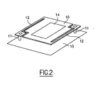
- FIG 2 is shown a simplified view of such a device.
- the bolometric device which is represented therein comprises a thin membrane 10 capable of absorbing infrared radiation, and suspended above a support 13 via anchoring points 11.
- a sensitive layer 14 is deposited on the membrane 10. Under the effect of infrared radiation, the membrane heats up and transmits its temperature to the layer 14.
- the electrical interconnection between the sensitive layer 14 and the reading elements (not shown) arranged on the substrate is ensured by a layer, generally metallic, not shown, passing through the anchoring points 11.
- the sensitivity of the thermal detection is significantly improved by introducing isolation arms 12 between the support substrate and the membrane in order to limit the thermal losses of the latter.
- the resistivity variations of the sensitive layer are recorded using two electrodes connected to a suitable reading circuit. The electrodes can be coplanar or sandwiched.
- the support substrate may consist of an integrated electronic circuit on a silicon wafer comprising, on the one hand, devices for stimulating and reading temperature variations and, on the other hand, the components of multiplexing that can serialize the signals from different thermometers and transmit them to a small number of outputs to be operated by a common imaging system.
- the membrane on which is deposited the thin layer of material according to the invention may consist for example of one or more layer (s) dielectric (s) including SiO, SiN.
- Electrodes including TiN having a high absorption of infrared radiation.
- the electrodes may be either affixed to the surface of the outer layer or enclosed between the two layers.
- the figure 3 shows two variants of integration of a thin layer of material according to the invention in a coplanar electrode detector.
- the structure supporting the ferrite is made of two insulating layers enclosing metal electrodes.
- the insulating layer deposited on the metal layer has contact openings so as to connect the ferrite sensitive element.
- the ferrite-supporting structure consists of a single insulating layer on which metal electrodes directly in contact with the ferrite sensitive element rest. In this configuration, it may be advantageous to deposit an absorbing layer infrared radiation on one of the faces of the structure.
- the etching of the ferrite makes it possible to disengage the material in the region of the isolation arms and in the regions separating the detectors from each other.
- the bolometric devices according to the invention may comprise a plurality of sensors in the form of a matrix array of pixels.
- a sensor array can be connected for example to a CCD or CMOS matrix.
- the device of the invention then constitutes an infrared camera.
- the bolometric devices of the invention can also be integrated in so-called monolithic structures, collectively manufactured by the microelectronics processes that have been developed for silicon.
- CMOS or CCD type of multiplexing circuit can be manufactured by directly connecting a matrix of sensitive elements to a CMOS or CCD type of multiplexing circuit.
- the support substrate may consist of an integrated electronic circuit comprising, on the one hand, stimulus and reading devices and, on the other hand, the multiplexing components which make it possible to serialize the signals coming from the different detectors and to transmit them to a number reduced outputs to be exploited by a conventional imaging system.
- the insulating supports are made in the form of thin layers having for example a thickness of 5 to 100 nm.
- These insulating elements for example SiN, SiO, ZnS, etc.
- PECVD plasma-assisted chemical vapor deposition
- the etching of these materials is generally performed by plasma etching methods.
- the metallic materials constituting the electrodes are preferably deposited by sputtering.
- the shape of the electrodes is defined by chemical etching or plasma methods.
- the thickness of the electrodes is for example between 5 nm and 100 nm.
- the electrodes which extend in the isolation arms are connected to the input stage of the read circuit by conventional methods of contact recovery, and are adapted to the structure of the micro-bridge (similar to the anchor points). 11 of the figure 2 ).
- the material is deposited in the form of a thin film according to the invention, using one of the techniques described above. Its etching can be carried out chemically (HCl, H 3 PO 4 ) or by specific plasma etching, or by ion milling.
- the invention also relates to a method for detecting infrared radiation or infrared imaging production, using a bolometric device capable of absorbing incident radiation, converting it to heat, and communicating a part heat generated at a sensitive element whose resistivity varies with temperature, wherein said device is as defined above.
- the device of the invention is usable in many fields of application, for example in the military field (devices for sighting and night exploration), in the industrial field (parts control), in the field of safety ( detection of fires, identification of victims in smoke-filled rooms, night surveillance of sites, assistance with night driving of vehicles), or in the medical field (blood circulation mapping, mammography, etc.).
- Example 1 Fe Fe magnetite thin layers 3 O 4
- Fe 3 O 4 magnetite particles are prepared by precipitation of iron hydroxides in a basic medium.
- the solution containing the precipitate is kept under an air sweep at 70 ° C. for four days.
- the oxide Fe 3 O 4 is gradually formed by oxidation and dehydration of the initial hydroxides. After washing and drying the precipitate, the particles were chamfered at 900 ° C. under a nitrogen atmosphere in order to reduce their specific surface area.
- the powder is mixed with an organic binder (polyvinyl alcohol) in the following proportions (by mass): 80% magnetite, 16% water, 4% polyvinyl alcohol. Then press the powder under a pressure of 55 tons in a matrix of 10 cm using a hydraulic press.
- the green compact obtained is densified by sintering at 950 ° C. under a nitrogen atmosphere to avoid the formation of the ⁇ -Fe 2 O 3 oxide.
- Radiocrystallographic analysis shows that the thin layers consist of a pure Fe 3 O 4 spinel phase.
- the electrical properties of the films in the raw state of deposit are as follows:
- the electrical properties are modified by thermal treatments under air (treatment duration: 2 hours) making it possible to modify the rate of cationic vacancies in the spinel structure.
- treatment duration 2 hours
- the results are shown in figure 1 which shows that such oxidation treatments make it possible to improve the sensitivity ⁇ .
- Radiocrystallographic analysis shows that the thin layers consist of a pure Fe 3 O 4 spinel phase.
- One sample is kept in the raw state of deposition (Example 2a) while two others are treated under air at 175 ° C. (Example 2b) and 250 ° C. (Example 2c) respectively for 2 hours so as to form Fe 3 O 4 + ⁇ .
- Example 2a Example 2b
- Example 2c Treatment Gross 175 ° C 250 ° C Resistivity (Ohm.cm) 1.6 27.6 715 Alpha (% .K -1 ) -1.9 -3.9 -4.5
- the ferrite powder is obtained by co-precipitation of hydroxides from nitrates of cobalt, copper, manganese and iron precipitated in triethylamine.
- the process for obtaining the sintered target is similar to that of Example 1.
- the sintering temperature is 900 ° C.
- the appropriate amounts of oxides (0.11 mole ZnO, 0.11 mole CuO and 0.44 mole Fe 2 O 3 ) are mixed and finely ground.
- the powder is chamotte at 750 ° C.
- the process for obtaining the sintered target is similar to that of Example 1.
- the sintering temperature is 900 ° C.
Landscapes
- Chemical & Material Sciences (AREA)
- Organic Chemistry (AREA)
- Inorganic Chemistry (AREA)
- Chemical Kinetics & Catalysis (AREA)
- General Physics & Mathematics (AREA)
- Spectroscopy & Molecular Physics (AREA)
- Physics & Mathematics (AREA)
- Engineering & Computer Science (AREA)
- Materials Engineering (AREA)
- Mechanical Engineering (AREA)
- Metallurgy (AREA)
- Photometry And Measurement Of Optical Pulse Characteristics (AREA)
- Inorganic Compounds Of Heavy Metals (AREA)
- Solid State Image Pick-Up Elements (AREA)
- Compounds Of Iron (AREA)
Description
- L'invention a pour objet l'utilisation de ferrites spinelles comme matériau sensible pour dispositifs bolométriques destinés à la détection de rayonnements infrarouges.
- On sait que les détecteurs bolométriques comportent un élément sensible à base d'un matériau dont la résistance électrique varie avec la température.
- Les dispositifs thermiques de détection de l'infrarouge sont capables d'absorber un rayonnement infrarouge incident et de le convertir en chaleur. L'augmentation de température de l'élément sensible qui en résulte engendre une variation de la résistance dudit élément sensible. Ces dispositifs permettent donc, à l'aide d'un montage électrique approprié, connu en soi, de convertir une modification de la température en signal électrique.
- Pour l'imagerie infrarouge, on utilise entre autre actuellement, comme caméras infrarouges, des microbolomètres comportant une pluralité de microcapteurs disposés sous la forme d'un réseau matriciel de pixels. Chaque microcapteur absorbe les radiations infrarouges qui le frappent, et les variations résultantes de température du matériau sensible, présent sous forme de couche mince dans chaque microcapteur, induisent une variation de la résistance électrique dudit matériau sensible. Un système de mesure, connu en soi, évalue les variations de la résistance et les traduit en signaux électriques. Ces signaux électriques peuvent être convertis en images à l'aide d'un dispositif d'imagerie approprié, connu en soi.
- On connaît des systèmes de détection et d'imagerie infrarouge ayant une bonne sensibilité, qui utilisent des matériaux sensibles à base de « HgCdTe » ou « YBaCuO ». Toutefois, ces systèmes présentent l'inconvénient de devoir être refroidis à la température de l'azote liquide.
- Il existe aussi des dispositifs bolométriques "non refroidis", dont le fonctionnement est basé notamment sur les variations de propriétés électriques du silicium amorphe ou de l'oxyde de vanadium. Ces dispositifs sont toutefois moins sensibles que les dispositifs refroidis.
- Des matériaux à base de perovskites ont également été préconisés. Ils présentent une sensibilité potentiellement intéressante, mais qui est contrebalancée par un bruit électronique intense.
- Il existe donc actuellement un besoin d'obtenir des dispositifs bolométriques non refroidis de détection de l'infrarouge ayant une bonne sensibilité et permettant une minimisation du bruit électronique.
- On a maintenant découvert que certains oxydes spinelles de métaux de transition, à base de fer, sont utilisables sous forme de couches minces comme matériau sensible pour des dispositifs bolométriques de détection de l'infrarouge. Ces matériaux, qui sont des ferrites spinelles, possèdent une résistivité électrique modérée et très sensible à la température. Ils permettent donc de faire des mesures électriques à fort rapport signal/bruit, et leur sensibilité peut être mise à profit pour déceler des rayonnements infrarouges de faible intensité, notamment dans la bande de longueurs d'onde de 8 à 12 micromètres.
- L'utilisation d'oxydes de structure spinelle dont le manganèse est l'élément majoritaire comme thermistances et non comme détecteurs d'infrarouge a été décrite dans les demandes de brevet
JP 2000-348905 A2 EP 1 058 276 A2 . Toutefois, ces oxydes sont des manganites et à ce titre différent des ferrites. Pour sa part l'article de A. Doctor, S. Baliga, M. Rost « Sputtered films thermistor IR detector » Proc. IEEE Mohawk Valley Dual-Use Technology and Applied Conférence, 153-156, 1993, propose des détecteurs bolométriques pour l'infrarouge utilisant des couches minces d'oxydes spinelles à base de nickel, de cobalt et de manganèse. Cet article décrit un mode de réalisation et d'utilisation de tels détecteurs IR en couches minces. Le brevetUS 5 854 587 décrit l'utilisation de manganites de type perovskites comme matériau sensible pour bolomètres. - Quant au document
FR 2 150 608 - L'invention concerne donc, selon un de ses aspects, l'utilisation comme matériau sensible en couche mince pour la détection bolométrique de radiations infrarouges, d'un matériau ayant une structure de ferrite spinelle dont la composition chimique, en dehors d'agents dopants éventuellement présents, répond à la formule brute I:
Fe3-(x+y) Mx Ay O4+δ (I)
dans laquelle le fer est l'élément métallique majoritaire,
M représente un métal ou une combinaison de deux ou plusieurs métaux de transition autre(s) que le fer,
A représente au moins un métal choisi parmi le magnésium et l'aluminium,
les métaux et l'oxygène sont sous forme d'ions,
x représente le nombre d'ions métalliques M, identiques ou différents,
y représente le nombre d'ions métalliques,
x peut varier de 0 à 2, et quelque soit x, x < 3-x-y
y peut varier de 0 à 0,5,
et
δ représente 0 ou un nombre positif, de valeur telle ou encore suffisamment faible pour que le produit de formule I contienne au moins un métal présent sous forme d'ions ayant deux états d'oxydation différents et situés sur un même sous-réseau de la structure spinelle. - Autrement dit, les produits de formule I, avec δ différent de zéro, sont des produits d'oxydation partielle, et non totale, des ferrites spinelles pour lesquels δ = 0, appelés ferrites spinelles stoechiométriques. Les raisons de cette caractéristique d'oxydation seulement partielle apparaîtront dans la suite de la description.
- La présente invention concerne en outre, selon un autre de ses aspects, un dispositif bolométrique pour la détection d'un rayonnement infrarouge ou pour l'imagerie infrarouge, comprenant au moins un capteur muni d'un élément sensible ayant la forme d'une couche mince d'un matériau ayant une structure de ferrite spinelle conforme à la présente invention.
- Elle se rapporte également, selon un autre de ses aspects, à un procédé de détection d'un rayonnement infrarouge ou de production d'imagerie infrarouge, à l'aide d'un dispositif bolométrique capable d'absorber un rayonnement incident, de le convertir en chaleur, et de communiquer une partie de la chaleur produite à un élément sensible dont la résistivité varie avec la température, dans lequel ledit dispositif est tel que défini ci-après.
- On sait que les oxydes de fer sont des composés ioniques, les métaux étant sous forme de cations, et l'oxygène sous forme d'anions Q2-.
- Dans la formule I selon l'invention, Fe représente l'ensemble des cations fer (ferreux et ferriques).
- Dans cette même formule, M figure un métal autre que le fer ou une combinaison de deux ou plusieurs métaux autres que le fer.
- En d'autres termes, M peut être symbolisé dans la formule générale I par la séquence Mx0M'x1M"x2 dans laquelle M, M', M" ... représentent des métaux de transition autres que le fer, et les indices x0, x1 et x2 représentent le nombre d'ions M, M', M"...
- M étant choisi parmi Co, Cu, Mn, Ni, Zn et Ti ou une de leurs combinaisons.
- On citera en particulier les ferrites de formule I dans lesquels M est un métal choisi parmi Co, Cu, Mn, Zn, Ni et Ti y compris ceux pour lesquels y est égal à zéro ou une de leurs combinaisons.
- On rappelle ci-après quelques propriétés connues des oxydes spinelles de métaux de transition, en prenant le cas des ferrites spinelles.
- On sait que la structure du spinelle (MgAl2O4) est également celle de la magnétite Fe3O4. On sait aussi que l'oxydation de la magnétite conduit au sesquioxyde de fer Fe2O3, qui conserve la structure cristalline de la magnétite, sous la forme dite γ-Fe2O3, jusqu'à une température de 400-500 °C environ, à laquelle l'oxyde γ-Fe2O3 se transforme en α-Fe2O3, ce dernier ayant la structure du corindon.
- On sait également que la structure de γ-Fe2O3, qui est obtenue par oxydation de la magnétite, est une structure de spinelle lacunaire. En effet, lors de l'oxydation de Fe3O4, le réseau d'anions O2- reste immuable. Des ions oxygène négatifs sont absorbés à la surface de l'oxyde. Ils s'arrangent selon une organisation identique à celle existant dans le réseau de la magnétite, dont ils constituent une extension. Les charges négatives ainsi apportées sont compensées par l'oxydation des ions ferreux en ions ferriques qui migrent, depuis l'intérieur du cristal, vers le nouvel arrangement d'anions oxygène dont ils assurent la cohésion en établissant des liaisons entre les cations Fe3+ et les anions O2-. Au terme de l'oxydation, la structure de type spinelle est conservée. Toutefois, le rapport cations/anions, initialement égal à 3/4, est devenu plus petit compte tenu de l'apport d'anions oxygène. Le cristal du produit oxydé comporte alors des sites normalement occupés par des ions métalliques (dans l'oxyde Fe3O4), qui sont devenus vacants, car abandonnés par les cations ayant migré à la surface. Ces sites sont encore appelés lacunes.
- Les ferrites spinelles dits stoechiométriques du type XaFe3-aO4, où X représente au moins un métal divalent et a <1, peuvent, tout comme la magnétite, être transformés en oxydes spinelles lacunaires, notamment par oxydation.
- Il est connu, en outre, qu'en introduisant dans les ferrites spinelles divers substituants, et notamment des métaux ayant des états de valence multiples, il est possible de créer des lacunes ou d'en faire varier le nombre.
- Par exemple, le remplacement d'une partie des ions Fe2+ par des ions trivalents, sans modifier le nombre de charges cationiques équilibrant les charges anioniques du réseau d'ions oxygène, peut se faire en remplaçant trois ions Fe2+ par deux ions trivalents. II y a donc dans ce cas remplacement de trois cations fer par deux ions seulement, et donc création d'une lacune.
- Inversement, si on remplace des ions Fe3+ par des ions divalents, la seule possibilité, pour conserver le nombre de charges cationiques, est de remplacer deux cations Fe3+ par trois cations divalents, à condition de pouvoir utiliser une lacune déjà présente dans le réseau. Ainsi, le remplacement de Fe3+ par un cation divalent conduit à une diminution du nombre de lacunes.
- On appelle « ferrites spinelles lacunaires déficients en cations » (ou ferrites spinelles sur-stoechiométriques) des composés du type spinelle à base de γ-Fe2O3 modifié par remplacement d'une partie des ions ferriques, et éventuellement des lacunes, par des cations métalliques autres que ferriques. Pour représenter les oxydes spinelles lacunaires sur-stoechiométriques, en gardant, dans la formule, un nombre d'atomes métalliques égal à trois (comme dans la formule Fe3O4), on est amené à écrire leur formule sous une forme du type Xx Fe3-x O4+δ, où Fe représente l'ion fer trivalent, X représente au moins un cation métallique autre que le cation ferrique, x est le nombre de cations X, tel que la somme du nombre de cations X et du nombre de cations ferriques est égale à 3, O représente un anion O2-, et δ est un nombre positif.
- Une autre façon de représenter les oxydes spinelles lacunaires surstoechiométriques, en gardant cette fois un nombre d'atomes d'oxygène égal à 4 (comme dans la formule Fe3O4), est d'écrire sa formule sous une forme équivalente faisant mention des lacunes :
Xx Fe3-x-y □y O4
dans laquelle le symbole □ représente les lacunes. - Ainsi, les ferrites spinelles stoechiométriques et les ferrites spinelles modérément lacunaires (incomplètement oxydés), comprennent, sous forme d'oxydes, au moins un même métal présent sous la forme de deux cations ayant des états d'ionisation différents. Ce sont donc des produits oxydables, cette oxydation se faisant avec formation de lacunes.
- Dans les formules précédentes, la valeur du nombre représenté par δ dépend de la nature des métaux présents et des conditions du traitement d'oxydation. En fait, le nombre δ correspond au nombre d'anions O2-, en plus de 4, qui est nécessaire pour compenser l'augmentation des charges des différents cations ayant été oxydés, afin d'assurer le maintien de la neutralité électrique. La détermination de δ (ou, ce qui revient au même, du nombre de lacunes) ne présente aucun intérêt en pratique. En fait, la mention de δ dans l'expression du nombre d'atomes oxygène de la formule brute I a surtout une valeur d'information qualitative, car elle permet de comprendre immédiatement que, lorsque δ n'est pas nul, la formule brute I représente un ferrite spinelle lacunaire. Dans les ferrites lacunaires de formule I, le nombre δ est généralement inférieur à 0,8 plus particulièrement inférieur à 0,5 environ et qualifie donc des ferrites lacunaires.
- L'obtention d'une couche mince du matériau sensible selon l'invention, sur un substrat approprié, peut être effectuée selon les techniques usuelles, notamment par pulvérisation cathodique, au départ d'une cible obtenue de façon classique par frittage d'un mélange de poudres d'oxydes des divers métaux choisis, et éventuellement d'agents dopants (ces derniers étant éventuellement sous forme d'oxydes).
- La technique de pulvérisation cathodique est un procédé de dépôt sur un substrat de couches minces d'un matériau quelconque, dans une enceinte contenant un gaz inerte, généralement de l'argon maintenu à pression réduite. Sous l'influence d'un champ électrique, le gaz est ionisé avec formation d'un plasma luminescent, et le choc des ions incidents sur le matériau, appelé « matériau-cible » ou « cible », qui est fixé sur une électrode soumise à un potentiel cathodique, provoque, par un effet mécanique, l'expulsion d'atomes de surface du matériau qui vont se déposer sur le substrat placé en face de la cible. En général, la composition du dépôt est voisine de la composition du matériau-cible.
- L'utilisation de tensions alternatives, en particulier à haute fréquence, présente divers avantages, notamment la pulvérisation de matériaux isolants et la possibilité d'utiliser des tensions d'amorçage plus faibles qu'en courant continu. Un tel procédé est appelé pulvérisation cathodique en radiofréquence (ou pulvérisation cathodique RF).
- Par superposition au champ électrique d'un champ magnétique au voisinage de la cathode (utilisation d'une cathode magnétron), on peut compliquer les trajectoires des électrons du plasma et augmenter ainsi l'ionisation du gaz, ce qui permet notamment d'obtenir une vitesse de dépôt plus importante pour une même puissance appliquée.
- Lorsque l'on souhaite déposer des oxydes métalliques en évitant le dépôt de formes totalement ou fortement oxydées, il est possible d'opérer avec de faibles pressions d'argon, par exemple 0.5 Pa. Inversement, si l'on souhaite obtenir un dépôt d'une forme oxydée, on peut opérer en présence d'un mélange d'argon et d'oxygène.
- Le dépôt peut aussi être effectué par les autres techniques connues d'élaboration en phase vapeur, comme par exemple l'évaporation sous vide, ou l'ablation laser.
- Les couches minces de ferrites spinelles utilisées selon l'invention sont des couches polycristallines.
- De préférence, la couche mince déposée a une composition proche du ferrite stoechiométrique (correspondant à δ = 0 ou voisin de 0). En déposant un matériau ayant sensiblement la composition du ferrite stoechiométrique, en atmosphère non oxydante, on obtient en effet des couches minces possédant la structure spinelle dont l'état cristallin est davantage satisfaisant que lorsque l'on dépose un ferrite plus oxydé ayant la composition souhaitée pour le produit final. En particulier, le dépôt sous forme de ferrite sensiblement stoechiométrique permet d'obtenir une couche mince de ferrite dont les dimensions des cristallites sont satisfaisantes. Il est ainsi possible d'obtenir des couches minces, d'épaisseur allant de 10 à 500 nm, et en particulier de 50 à 150 nm, constituées de cristallites dont la taille moyenne varie entre 5 et 50 nm environ, et en particulier entre 10 et 30 nm environ. Ces caractéristiques dimensionnelles, grâce à la faible épaisseur de la couche, permettent en effet de minimiser l'inertie thermique de la couche sensible et, grâce à la faible taille des cristallites, de minimiser la dispersion du bruit électronique d'un pixel à l'autre, lors de la détection bolométrique. Par exemple, en effectuant le dépôt par pulvérisation cathodique radiofréquence, sous une pression d'argon pouvant aller de 0,1 à 2,5 Pa, il est possible d'obtenir des compositions de ferrites présentant les caractéristiques qui viennent d'être indiquées.
- On appelle « cristallites » les microcristaux constituant la couche mince. Ce sont des domaines cristallins qui diffractent de manière cohérente les rayons X. Autrement dit, ce sont des monocristaux dont les dimensions moyennes peuvent être facilement déterminées, notamment par microscopie électronique à transmission, microscopie à force atomique ou par diffraction des rayons X.
- D'une façon générale, les compositions de ferrites spinelles lacunaires peuvent être modifiées par des agents dopants, qui ne sont pas représentés par la formule I, et qui ne font pas nécessairement partie du réseau cristallin. L'utilisation d'un grand nombre d'agents dopants a été décrite pour ce type de composés. La présence d'agents dopants peut par exemple faciliter la régulation de la cristallisation. Généralement, les agents dopants sont présents sous forme d'oxydes dans une proportion pondérale ne dépassant pas 1 à 2 % en poids, par rapport au poids de l'oxyde spinelle. Les agents dopants sont par exemple le silicium, le phosphore, le bore, des métaux alcalino-terreux (en particulier Ca, Ba, Sr), des métaux alcalins (par exemple Na, K, Li), le gallium, le germanium, l'arsenic, l'indium, l'antimoine, le bismuth, le plomb, etc.
- Lors du dépôt de mélanges d'oxydes ayant sensiblement la composition d'oxydes spinelles de type stoechiométrique, dépôt éventuellement suivi d'un traitement thermique en atmosphère oxydante, la couche mince déposée adopte spontanément une structure cristalline de spinelle.
- Après le dépôt de la couche mince ayant sensiblement la composition d'un oxyde spinelle de type stoechiométrique, il convient généralement d'effectuer un traitement d'oxydation pour faire apparaître des lacunes. La faible épaisseur des couches déposées ainsi que la faible taille des cristallites facilitent une oxydation à une température modérée, généralement inférieure ou égale à 300 °C. Lors de ce traitement d'oxydation, la couche mince acquiert la structure de spinelle lacunaire, et on constate que ce traitement d'oxydation permet généralement d'augmenter la variation de la résistivité avec la température, qui représente la propriété de sensibilité recherchée pour les matériaux actifs des dispositifs bolométriques.
- Les ferrites spinelles stoechiométriques ou lacunaires utilisés selon l'invention ont des propriétés de semi-conducteurs. En effet, leur conductivité augmente avec la température : ce sont des produits dits à coefficient de température négatif. De tels produits sont caractérisés par leur énergie d'activation, Ea, calculée selon la formule
Ea*=k B,
avec
k représentant la constante de Boltzman et
B la constante énergétique, qui correspond à la pente de la courbe représentant Log R en fonction de 1/T avec R désignant la résistance électrique et T la température. - En particulier, l'énergie d'activation Ea peut être calculée à partir de deux mesures de résistance, R1 et R2, effectuées respectivement aux températures T1 et T2 :

- On exprime la sensibilité d'un matériau pour détecteur bolométrique à l'aide du coefficient de température α qui représente la dérivée de la résistance par rapport à la température, divisée par la résistance :

- Le coefficient α est exprimé en %.Kelvin-1 (%.K-1).
- Il est admis actuellement que la conduction électronique dans les oxydes de métaux de transition n'est possible qu'entre cations d'un même élément possédant des états d'ionisation différant d'une unité et placés sur un même sous-réseau de la structure spinelle (loi de Verwey). La conduction se fait par un mécanisme de transition par sauts, désigné en langue anglaise par le terme « hopping ».
- L'oxydation des ferrites spinelles stoechiométriques en ferrites spinelles lacunaires abaisse le nombre de couples de cations (notamment couples Fe2+-Fe3+) permettant le phénomène de hopping et augmente donc la résistivité du matériau. Par exemple, dans le cas de l'oxydation totale de la magnétite, le produit obtenu, c'est-à-dire γ-Fe2O3, est totalement isolant. Il convient donc d'éviter une oxydation totale du ferrite spinelle, qui rendrait le matériau non conducteur, en jouant sur les facteurs suivants :
- durée du traitement thermique oxydant, à une température généralement inférieure à 350 °C, et en particulier inférieure ou égale à 300 °C,
- pression partielle d'oxygène.
- On peut notamment opérer à l'air, la durée de traitement pouvant aller par exemple de 30 minutes à 3 heures.
- Il faut évidemment éviter une oxydation totale qui augmente trop fortement la résistance, le matériau n'étant alors plus conducteur, comme on vient de le voir.
- On constate que le traitement d'oxydation augmente la résistivité mais généralement augmente aussi le coefficient de température α. On peut donc déterminer par de simples expériences de routine les conditions du traitement d'oxydation qui permettent éventuellement d'obtenir, pour une composition en métaux donnée, les degrés d'oxydation donnant une valeur optimale du coefficient α, ou une valeur de α supérieure, en valeur absolue, à une valeur seuil prédéterminée (par exemple > 1 %.K-1). De la même façon, on peut sélectionner, avec de telles expériences de routine, des compositions de métaux de transition qui permettent d'obtenir des propriétés de résistivité intéressantes, ou d'optimiser les proportions relatives des métaux de telles compositions.
- Dans une phase de recherche, le procédé d'obtention d'une couche sensible de ferrite spinelle selon l'invention consiste donc à déposer une couche ayant sensiblement une composition de ferrite spinelle stoechiométrique, et à effectuer si nécessaire des traitements d'oxydation permettant éventuellement d'améliorer la valeur de α, afin de sélectionner les compositions dont la valeur absolue de α est, par exemple, supérieure à 1 %.K-1 ou à une autre valeur souhaitée tout en conservant une résistivité et un bruit électronique faibles. La couche mince est généralement déposée sur une ou plusieurs couches aptes à assurer la rigidité mécanique, l'absorption du rayonnement infrarouge et les connexions électriques de la couche sensible. Cette couche mince ou l'ensemble des couches peut (peuvent) être déposée(s) sur une structure sacrificielle.
- Comme précisé précédemment, un autre aspect de l'invention concerne un dispositif bolométrique pour la détection d'un rayonnement infrarouge ou pour l'imagerie infrarouge, comprenant au moins un capteur muni d'un élément sensible ayant la forme d'une couche mince de matériau telle que définie précédemment
- Dans un mode de réalisation particulier du dispositif bolométrique de l'invention, le capteur, qui est inséré dans un boîtier comportant une fenêtre d'entrée transparente à l'infrarouge, comprend une membrane capable d'absorber un rayonnement infrarouge et de le convertir en chaleur, ladite membrane étant disposée de façon à pouvoir être exposée à un rayonnement infrarouge incident ayant traversé la fenêtre d'entrée, et de façon à transmettre une partie de la chaleur ainsi produite audit élément sensible. En
figure 2 est représentée une vue simplifiée d'un tel dispositif. - Le dispositif bolométrique qui y est représenté comprend une fine membrane 10 capable d'absorber le rayonnement infrarouge, et suspendue au-dessus d'un support 13 par l'intermédiaire de points d'ancrage 11. Une couche sensible 14 est déposée sur la membrane 10. Sous l'effet d'un rayonnement infrarouge, la membrane s'échauffe et transmet sa température à la couche 14. L'interconnexion électrique entre la couche sensible 14 et les éléments de lecture (non représentés) disposés sur le substrat est assurée par une couche, généralement métallique, non représentée, passant par les points d'ancrage 11. La sensibilité de la détection thermique est notablement améliorée en introduisant des bras d'isolement 12 entre le substrat support et la membrane afin de limiter les pertes thermiques de cette dernière. Les variations de résistivité de la couche sensible sont enregistrées à l'aide de deux électrodes reliées à un circuit de lecture approprié. Les électrodes peuvent être soit coplanaires, soit en regard (sandwich).
- Dans les dispositifs bolométriques selon l'invention, le substrat support peut être constitué d'un circuit électronique intégré sur une plaquette de silicium comprenant d'une part des dispositifs de stimuli et de lecture des variations de températures et d'autre part les composants de multiplexage qui permettent de sérialiser les signaux issus des différents thermomètres et de les transmettre vers un nombre réduit de sorties afin d'être exploités par un système d'imagerie usuel.
- En ce qui concerne la membrane sur laquelle est déposée la couche mince de matériau selon l'invention, elle peut être constituée par exemple d'une ou plusieurs couche(s) diélectrique(s) notamment de SiO, SiN.
- Dans le cas d'une unique couche, celle-ci peut être recouverte partiellement par des électrodes notamment de TiN possédant une forte absorption du rayonnement infrarouge. Dans le cas de deux couches, les électrodes peuvent être soit apposées en surface de la couche externe soit enfermées entre les deux couches.
- La
figure 3 rend compte de deux variantes d'intégration d'une couche mince de matériau selon l'invention dans un détecteur à électrodes coplanaires. - En
figure 3A , la structure supportant le ferrite est constituée de deux couches isolantes enfermant des électrodes métalliques. La couche isolante déposée sur la couche métallique comporte des ouvertures de contact de manière à connecter l'élément sensible en ferrite. - En
figure 3B , la structure supportant la ferrite est constitué d'une unique couche isolante sur laquelle reposent des électrodes métalliques directement en contact avec l'élément sensible en ferrite. Dans cette configuration, il peut être intéressant de déposer une couche absorbante le rayonnement infrarouge sur l'une des faces de la structure. - Dans ces deux variantes de réalisation, la gravure de la ferrite permet de dégager le matériau dans la région des bras d'isolement et dans les régions séparant les détecteurs entre eux.
- Ces deux modes de réalisation conduisent avantageusement à un composant optimisé en termes de signal sur bruit.
- Il est entendu que les dispositifs bolométriques conformes à l'invention peuvent comprendre une pluralité de capteurs sous la forme d'un réseau matriciel de pixels. Un tel réseau de capteurs peut être connecté par exemple à une matrice CCD ou CMOS. Avec un système d'imagerie approprié, le dispositif de l'invention constitue alors une caméra infrarouge.
- Les dispositifs bolométriques de l'invention peuvent également être intégrés dans des structures dites monolithiques, fabriquées de manière collective par les procédés de micro-électronique qui ont été développés pour le silicium.
- Ainsi, des imageurs infrarouges monolithiques, fonctionnant à température ambiante, peuvent être fabriqués en connectant directement une matrice d'éléments sensibles à un circuit de multiplexage de type CMOS ou CCD. Le substrat support peut être constitué d'un circuit électronique intégré comprenant d'une part des dispositifs de stimulis et de lecture et d'autre part les composants de multiplexage qui permettent de sérialiser les signaux issus des différents détecteurs et de les transmettre vers un nombre réduit de sorties pour être exploités par un système d'imagerie usuelle.
- Dans de tels dispositifs, les supports isolants sont réalisés sous forme de couches minces ayant par exemple une épaisseur de 5 à 100 nm. Ces éléments isolants (par exemple SiN, SiO, ZnS, etc.) sont obtenus à l'aide des techniques de dépôt à basse température habituellement utilisées pour ces matériaux, telles que la pulvérisation cathodique ou le dépôt chimique en phase vapeur assisté plasma (PECVD). La gravure de ces matériaux est généralement réalisée par des procédés d'attaque chimique assistée par plasma.
- Les matériaux métalliques constituant les électrodes (par exemple Ti, TiN, Pt, etc.) sont préférentiellement déposés par pulvérisation cathodique. La forme des électrodes est définie par des procédés de gravure chimique ou par plasma. L'épaisseur des électrodes est comprise par exemple entre 5 nm et 100 nm. Les électrodes qui se prolongent dans les bras d'isolement sont connectées à l'étage d'entrée du circuit de lecture par des procédés classiques de reprise de contact, et sont adaptées à la structure du micro-pont (analogue aux points d'ancrage 11 de la
figure 2 ). - Le matériau est déposé sous l'aspect d'une couche mince selon l'invention, à l'aide d'une des techniques décrites précédemment Sa gravure peut être réalisée par voie chimique (HCl, H3PO4) ou par des procédés de gravure plasma spécifiques, ou encore par usinage ionique.
- L'invention concerne également un procédé de détection d'un rayonnement infrarouge ou de production d'imagerie infrarouge, à l'aide d'un dispositif bolométrique capable d'absorber un rayonnement incident, de le convertir en chaleur, et de communiquer une partie de la chaleur produite à un élément sensible dont la résistivité varie avec la température, dans lequel ledit dispositif est tel que défini précédemment.
- Le dispositif de l'invention est utilisable dans de nombreux domaines d'application, par exemple dans le domaine militaire (dispositifs de visée et d'exploration nocturne), dans le domaine industriel (contrôle de pièces), dans le domaine de la sécurité (détection d'incendies, repérage de victimes dans des pièces enfumées, surveillance nocturne des sites, assistance à la conduite nocturne de véhicules), ou dans le domaine médical (cartographie de circulation sanguine, mammographie, etc.).
- Les exemples et figures qui suivent sont présentés à titre illustratif et non limitatif du domaine de l'invention.
- la
figure 1 représente les variations de la résistivité et de α de la couche mince décrite à l'exemple 1, en fonction de la température du traitement thermique oxydant, et de l'épaisseur, - la
figure 2 représente schématiquement une vue en perspective simplifiée d'un mode de réalisation d'un dispositif bolométrique selon l'invention, - la
figure 3 illustre deux variantes d'intégration d'une couche mince du matériau selon l'invention dans un dispositif bolométrique selon l'invention. - On prépare des particules de magnétite Fe3O4 par précipitation d'hydroxydes de fer en milieu basique. La solution comportant le précipité est maintenue sous balayage d'air à 70 °C pendant quatre jours. L'oxyde Fe3O4 se forme progressivement par oxydation et déshydratation des hydroxydes initiaux. Après avoir lavé et séché le précipité, on effectue un chamottage des particules à 900 °C sous atmosphère d'azote pour diminuer leur surface spécifique.
- A l'issue de ce traitement, on mélange la poudre à un liant organique (alcool polyvinylique) dans les proportions suivantes (en masse) : 80% de magnétite, 16% d'eau, 4% d'alcool polyvinylique. On effectue ensuite le pressage de la poudre sous une pression de 55 tonnes dans une matrice de 10cm à l'aide d'une presse hydraulique. Le compact cru obtenu est densifiée par frittage à 950 °C sous atmosphère d'azote pour éviter la formation de l'oxyde α- Fe2O3.
- L'élaboration de la couche mince est effectuée avec un bâti de pulvérisation cathodique de type SCM400 (Alcatel CIT), fonctionnant en mode radio-fréquence. Le substrat est du silicium recouvert d'une couche de SiO2 de 1 µm d'épaisseur. Le dépôt de ferrite est effectué dans les conditions citées ci-après:
- Plasma d'argon
- Pression d'enceinte: 0,5 Pa
- Distance cible-substrat: 5 cm
- Densité de puissance RF: 3,1 W/cm2
- Sans magnétron
- Vitesse de dépôt: 4.5 nm/min
- Les épaisseurs voulues sont obtenues en faisant varier les temps de dépôt :
Exemple 1a Exemple 1b Epaisseur (nm) 50 100 Résistivité (Ohm.cm) 0,012 0,021 Alpha (%.K-1) -1,2 -1,2 - Exemple la, épaisseur = 50 nm, temps de dépôt =11 minutes,
- Exemple 1b, épaisseur =100 nm, temps de dépôt = 22 minutes.
- L'analyse radiocristallographique montre que les couches minces sont constituées d'une phase spinelle pure Fe3O4. Les propriétés électriques des films à l'état brut de dépôt sont les suivantes:
- On modifie les propriétés électriques par des traitements thermiques sous air (durée du traitement : 2 heures) permettant de modifier le taux de lacunes cationiques dans la structure spinelle. Les résultats sont représentés à la
figure 1 , qui montre que de tels traitements d'oxydation permettent d'améliorer la sensibilité α. - On prépare des couches minces de magnétite Fe3O4 par une méthode analogue à celle décrite dans l'exemple 1. Les substrats sont identiques, mais les conditions de dépôt diffèrent, et sont les suivantes :
- Plasma d'argon
- Pression d'enceinte: 2 Pa
- Distance cible-substrat: 5 cm
- Densité de puissance RF : 0,75 W/cm2
- Avec magnétron
- Epaisseur du dépôt : 100 nm
- L'analyse radiocristallographique montre que les couches minces sont constituées d'une phase spinelle pure Fe3O4. Un échantillon est gardé à l'état brut de dépôt (Exemple 2a) tandis que deux autres sont traités sous air respectivement à 175 °C (Exemple 2b) et 250 °C (Exemple 2c) pendant 2 heures de manière à, former Fe3O4+δ.
- Les propriétés électriques des films sont les suivantes :
Exemple 2a Exemple 2b Exemple 2c Traitement Brut 175 °C 250 °C Résistivité (Ohm.cm) 1,6 27,6 715 Alpha (%.K-1) -1,9 -3,9 -4,5 - La poudre de ferrite est obtenue par co-précipitation d'hydroxydes à partir de nitrates de cobalt, cuivre, manganèse et fer précipités dans la triéthylamine. Le procédé d'obtention de la cible frittée est analogue à celui de l'exemple 1. La température de frittage est de 900 °C.
- Les couches minces sont déposées sur un substrat de verre de 1,2 mm d'épaisseur. Les conditions de dépôt sont les suivantes :
- Plasma d'argon
- Pression d'enceinte: 0,5 Pa
- Distance cible-substrat: 5 cm
- Densité de puissance RF : 2 W/cm2
- Avec magnétron
- Epaisseur du dépôt : 300 nm
- Après traitement thermique sous air à 300 °C pendant 2 heures, les propriétés électriques du film sont les suivantes :
- Résistivité = 1150 Ohm.cm,
- Alpha = -2,7 %.K-1
- Les quantités appropriées d'oxydes (0,11 mole ZnO ; 0,11 mole CuO et 0,44 mole de Fe203) sont mélangées et finement broyées. La poudre est chamottée à 750 °C. Le procédé d'obtention de la cible frittée est analogue à celui de l'exemple 1. La température de frittage est de 900 °C.
- Les couches minces sont déposées sur un substrat de verre de 1,2 mm d'épaisseur. Les conditions de dépôt sont les suivantes:
- Plasma d'argon
- Pression d'enceinte: 0,5 Pa
- Distance cible-substrat: 5,5 cm
- Densité de puissance RF : 2,75 W/cm2
- Sans magnétron
- Epaisseur du dépôt: 125 nm.
- Les propriétés électriques du film à l'état brut de dépôt sont les suivantes :
- Résistivité = 0,28 Ohm.cm,
- Alpha = -1,1 %.K-1
Claims (6)
- Utilisation comme matériau sensible en couche mince pour la détection bolométrique de radiations infrarouges, d'un matériau ayant une structure de ferrite spinelle dont la composition chimique, en dehors d'agents dopants éventuellement présents, répond à la formule brute I :
Fe3-(x+y)MxAyO4+δ (I)
dans laquelle le fer est l'élément métallique majoritaire,
M représente un métal ou une combinaison de deux ou plusieurs métaux de transition autres que le fer, M étant choisi parmi Co, Cu, Mn, Ni, Zn et Ti ou une de leurs combinaisons,
A représente au moins un métal choisi parmi le magnésium et l'aluminium,
les métaux et l'oxygène sont sous forme d'ions,
x représente le nombre d'ions métalliques M, identiques ou différents,
y représente le nombre d'ions métalliques A,
x peut varier de 0 à 2, et quelque soit x, x < 3-x-y
y peut varier de 0 à 0,5,
et
δ représente 0 ou un nombre positif, suffisamment faible pour que le produit de formule I contienne au moins un métal présent sous forme d'ions ayant deux états d'oxydation différents et situés sur un même sous-réseau de la structure spinelle,
les agents dopants éventuellement présents étant présents sous forme d'oxydes dans une proportion pondérale ne dépassant pas 1 à 2 % en poids, par rapport au poids de l'oxyde spinelle, et choisis parmi le silicium, le phosphore, le bore, des métaux alcalino-terreux, en particulier Ca, Ba, Sr, des métaux alcalins, par exemple Na, K, Li, le gallium, le germanium, l'arsenic, l'indium, l'antimoine, le bismuth, le plomb. - Dispositif bolométrique pour la détection d'un rayonnement infrarouge ou pour l'imagerie infrarouge, comprenant au moins un capteur muni d'un élément sensible ayant la forme d'une couche mince telle que définie en revendication 1.
- Dispositif bolométrique selon la revendication 2, dans lequel ledit capteur, inséré dans un boîtier comportant une fenêtre d'entrée transparente à l'infrarouge, comprend une membrane capable d'absorber un rayonnement infrarouge et de le convertir en chaleur, ladite membrane étant disposée de façon à pouvoir être exposée à un rayonnement infrarouge incident ayant traversé la fenêtre d'entrée, et de façon à transmettre une partie de la chaleur ainsi produite audit élément sensible.
- Dispositif selon la revendication 2 ou 3, comprenant une pluralité desdits capteurs sous la forme d'un réseau de pixels.
- Dispositif selon la revendication 4, dans lequel ledit réseau est connecté à une matrice CCD ou CMOS.
- Procédé de détection d'un rayonnement infrarouge ou de production d'imagerie infrarouge, à l'aide d'un dispositif bolométrique capable d'absorber un rayonnement incident, de le convertir en chaleur, et de communiquer une partie de la chaleur produite à un élément sensible dont la résistivité varie avec la température, dans lequel ledit dispositif est tel que défini dans l'une quelconque des revendications 2 à 5.
Applications Claiming Priority (2)
| Application Number | Priority Date | Filing Date | Title |
|---|---|---|---|
| FR0315190A FR2864065B1 (fr) | 2003-12-22 | 2003-12-22 | Utilisation de ferrites spinelles comme materiau sensible pour dispositifs bolometriques de detection de l'infrarouge. |
| PCT/FR2004/050695 WO2005064294A1 (fr) | 2003-12-22 | 2004-12-15 | Utilisation de ferrites spinelles comme materiau sensible pour dispositifs bolometriques de detection de l'infrarouge. |
Publications (2)
| Publication Number | Publication Date |
|---|---|
| EP1697706A1 EP1697706A1 (fr) | 2006-09-06 |
| EP1697706B1 true EP1697706B1 (fr) | 2015-04-01 |
Family
ID=34630465
Family Applications (1)
| Application Number | Title | Priority Date | Filing Date |
|---|---|---|---|
| EP04816549.2A Expired - Lifetime EP1697706B1 (fr) | 2003-12-22 | 2004-12-15 | Utilisation de ferrites spinelles comme materiau sensible pour dispositifs bolometriques de detection de l infrarouge. |
Country Status (5)
| Country | Link |
|---|---|
| US (1) | US8017911B2 (fr) |
| EP (1) | EP1697706B1 (fr) |
| JP (1) | JP4521407B2 (fr) |
| FR (1) | FR2864065B1 (fr) |
| WO (1) | WO2005064294A1 (fr) |
Families Citing this family (15)
| Publication number | Priority date | Publication date | Assignee | Title |
|---|---|---|---|---|
| FR2864065B1 (fr) * | 2003-12-22 | 2006-02-24 | Univ Toulouse | Utilisation de ferrites spinelles comme materiau sensible pour dispositifs bolometriques de detection de l'infrarouge. |
| FR2910125B1 (fr) * | 2006-12-14 | 2013-07-05 | Commissariat Energie Atomique | Utilisation d'association de monoxyde de fer et d'oxydes spinelles comme materiau sensible destine a la detection de rayonnements infrarouges |
| FR2941297B1 (fr) * | 2009-01-19 | 2011-02-11 | Commissariat Energie Atomique | Procede de fabrication d'un detecteur bolometrique |
| JP2011153871A (ja) * | 2010-01-26 | 2011-08-11 | Seiko Epson Corp | 熱型光検出器、熱型光検出装置及び電子機器 |
| JP5624931B2 (ja) * | 2011-04-13 | 2014-11-12 | キヤノンアネルバ株式会社 | スピネルフェライト薄膜の製造方法 |
| CN102280455B (zh) * | 2011-05-11 | 2013-01-09 | 武汉高德红外股份有限公司 | 一种非制冷式红外焦平面阵列探测器 |
| FR2999805B1 (fr) * | 2012-12-17 | 2017-12-22 | Commissariat Energie Atomique | Procede de realisation d'un dispositif de detection infrarouge |
| CN106949978A (zh) * | 2017-02-13 | 2017-07-14 | 清华大学 | 一种热成像传感器像素单元及其阵列 |
| US10770605B2 (en) | 2017-04-20 | 2020-09-08 | King Abdulaziz University | Photodiode with spinel oxide photoactive layer |
| KR101832408B1 (ko) | 2017-07-19 | 2018-02-26 | 한국세라믹기술원 | 볼로미터용 산화물 저항 박막 및 그 제조방법 |
| KR102156664B1 (ko) * | 2018-12-18 | 2020-09-16 | 한국세라믹기술원 | 볼로미터용 산화물 저항 박막 및 그 제조방법 |
| GB201821211D0 (en) * | 2018-12-24 | 2019-02-06 | Lussey David | New composition of matter |
| EP3933357B1 (fr) * | 2019-02-28 | 2023-11-01 | Panasonic Intellectual Property Management Co., Ltd. | Capteur infrarouge et réseau de capteurs infrarouges |
| FR3099573B1 (fr) * | 2019-07-30 | 2021-07-23 | Commissariat Energie Atomique | Procédé de fabrication d’un microbolomètre comportant un matériau sensible à base d’oxyde de vanadium |
| CN112577576B (zh) * | 2020-11-10 | 2024-12-17 | 河南中烟工业有限责任公司 | 自动称量装置 |
Family Cites Families (18)
| Publication number | Priority date | Publication date | Assignee | Title |
|---|---|---|---|---|
| FR2150608A1 (en) * | 1971-08-30 | 1973-04-13 | Coron Noel | Bolometric infra-red ray detector - with iron oxide powder/ferrite surface |
| FR2506294A1 (fr) * | 1981-05-19 | 1982-11-26 | Shell France | Composition ayant une structure de spinelle |
| US4531110A (en) * | 1981-09-14 | 1985-07-23 | At&T Bell Laboratories | Negative temperature coefficient thermistors |
| FR2624846B1 (fr) * | 1987-12-16 | 1990-05-04 | Atochem | Composition a base d'un oxyde de structure spinelle, son application comme catalyseur et procede pour l'obtenir |
| SE465596B (sv) * | 1990-02-16 | 1991-09-30 | Asea Brown Boveri | Seriekondensatorutrustning med styrbar krets foer daempning av subsynkrona resonanssvaengningar |
| US5821598A (en) * | 1995-02-01 | 1998-10-13 | Research Corporation Technologies, Inc. | Uncooled amorphous YBaCuO thin film infrared detector |
| US5962854A (en) * | 1996-06-12 | 1999-10-05 | Ishizuka Electronics Corporation | Infrared sensor and infrared detector |
| FR2752299B1 (fr) * | 1996-08-08 | 1998-09-11 | Commissariat Energie Atomique | Detecteur infrarouge et procede de fabication de celui-ci |
| JPH10163510A (ja) | 1996-12-04 | 1998-06-19 | Mitsubishi Electric Corp | 赤外線検知素子 |
| EP0867701A1 (fr) * | 1997-03-28 | 1998-09-30 | Interuniversitair Microelektronica Centrum Vzw | Procédé de réalisation d'un détecteur de rayonnement sensible à l'infrarouge, notamment un bolomètre sensible à l'infrarouge |
| JPH10281864A (ja) * | 1997-04-03 | 1998-10-23 | Nikon Corp | 熱型赤外線カメラ |
| US5854587A (en) * | 1997-06-26 | 1998-12-29 | The United States Of America As Represented By The Secretary Of The Navy | REx M1-x Mny O.sub.δ films for microbolometer-based IR focal plane arrays |
| FR2781927B1 (fr) * | 1998-07-28 | 2001-10-05 | Commissariat Energie Atomique | Dispositif de detection de rayonnements multispectraux infrarouge/visible |
| CN1118103C (zh) * | 1998-10-21 | 2003-08-13 | 李韫言 | 微细加工热辐射红外传感器 |
| JP2002250655A (ja) | 2001-02-26 | 2002-09-06 | Mitsubishi Electric Corp | 赤外線検知素子およびその製造方法 |
| FR2864065B1 (fr) * | 2003-12-22 | 2006-02-24 | Univ Toulouse | Utilisation de ferrites spinelles comme materiau sensible pour dispositifs bolometriques de detection de l'infrarouge. |
| FR2910125B1 (fr) * | 2006-12-14 | 2013-07-05 | Commissariat Energie Atomique | Utilisation d'association de monoxyde de fer et d'oxydes spinelles comme materiau sensible destine a la detection de rayonnements infrarouges |
| FR2941297B1 (fr) * | 2009-01-19 | 2011-02-11 | Commissariat Energie Atomique | Procede de fabrication d'un detecteur bolometrique |
-
2003
- 2003-12-22 FR FR0315190A patent/FR2864065B1/fr not_active Expired - Fee Related
-
2004
- 2004-12-15 US US10/582,520 patent/US8017911B2/en not_active Expired - Fee Related
- 2004-12-15 JP JP2006544519A patent/JP4521407B2/ja not_active Expired - Fee Related
- 2004-12-15 WO PCT/FR2004/050695 patent/WO2005064294A1/fr not_active Ceased
- 2004-12-15 EP EP04816549.2A patent/EP1697706B1/fr not_active Expired - Lifetime
Also Published As
| Publication number | Publication date |
|---|---|
| JP4521407B2 (ja) | 2010-08-11 |
| US20070120059A1 (en) | 2007-05-31 |
| FR2864065B1 (fr) | 2006-02-24 |
| JP2007517387A (ja) | 2007-06-28 |
| EP1697706A1 (fr) | 2006-09-06 |
| WO2005064294A1 (fr) | 2005-07-14 |
| US8017911B2 (en) | 2011-09-13 |
| FR2864065A1 (fr) | 2005-06-24 |
Similar Documents
| Publication | Publication Date | Title |
|---|---|---|
| FR2864065A1 (fr) | Utilisation de ferrites spinelles comme materiau sensible pour dispositifs bolometriques de detection de l'infrarouge. | |
| CA2671945C (fr) | Utilisation d'association de monoxyde de fer et d'oxydes spinelles comme materiau sensible destine a la detection de rayonnements infrarouges | |
| Kumar et al. | Pulsed laser deposited vanadium oxide thin films for uncooled infrared detectors | |
| US8502639B1 (en) | Nanocomposite semiconducting material with reduced resistivity | |
| Karunagaran et al. | Study of a pulsed laser deposited vanadium oxide based microbolometer array | |
| EP2894444A1 (fr) | Matériau sensible pour la détection bolométrique | |
| JP2000095522A (ja) | ペロブスカイト型マンガン酸化物薄膜、その製造方法及びそれを用いた赤外線検出素子 | |
| US11499871B2 (en) | Detector of electromagnetic radiation | |
| WO2022158199A1 (fr) | Élément de détection thermique et capteur d'image | |
| CN111403585A (zh) | 一种基于铋硒碲薄膜材料的光、热探测器及其制备方法 | |
| WO2000068999A1 (fr) | Dispositif de detection de rayons x ou gamma et procede de fabrication de ce dispositif | |
| WO1996031640A1 (fr) | Couches minces d'alliages quasi-cristallins, leur preparation et leurs utilisations | |
| CN115394767B (zh) | 一种cmos直接集成的红外探测器结构及其工艺 | |
| Hai et al. | Uncooled silicon germanium oxide (Si [sub] x [/sub] Ge [sub] y [/sub] O [sub] 1-xy [/sub]) thin films for infrared detection | |
| Cole et al. | High performance infrared detector arrays using thin film microstructures | |
| Al-Khalli et al. | Tuning of zinc oxide temperature sensing and optical absorption properties by tin heavy-doping | |
| CN114107924B (zh) | 一种非制冷红外微测辐射热计用热敏薄膜 | |
| CA3146045A1 (fr) | Procede de fabrication d'un microbolometre comportant un materiau sensible a base d'oxyde de vanadium | |
| KR20030019772A (ko) | 비냉각 방식의 열 감지 센서용 바나듐 다이옥사이드박막의 제조방법 | |
| Zhou et al. | Optimizing Laser‐Induced Voltage Signal in SnO2 Thin Films by Changing Oxygen Pressure | |
| Lee et al. | Electric characteristic of nickel oxide film for the mirobolometer | |
| Kleto et al. | Ion-plasma protective coatings of CdTe surface for X-and gamma-ray detectors | |
| Nam et al. | Structural and electrical properties of vanadium tungsten oxide thin films grown on Pt/TiO2/SiO2/Si substrates | |
| CN120129332A (zh) | 一种逆向光敏介电特性的复合氧化物电容器及其制备方法 | |
| Rana et al. | Amorphous Ge x Si 1-x O y: H Microbolometers with High Responsivity |
Legal Events
| Date | Code | Title | Description |
|---|---|---|---|
| PUAI | Public reference made under article 153(3) epc to a published international application that has entered the european phase |
Free format text: ORIGINAL CODE: 0009012 |
|
| 17P | Request for examination filed |
Effective date: 20060602 |
|
| AK | Designated contracting states |
Kind code of ref document: A1 Designated state(s): AT BE BG CH CY CZ DE DK EE ES FI FR GB GR HU IE IS IT LI LT LU MC NL PL PT RO SE SI SK TR |
|
| 17Q | First examination report despatched |
Effective date: 20060929 |
|
| DAX | Request for extension of the european patent (deleted) | ||
| RAP1 | Party data changed (applicant data changed or rights of an application transferred) |
Owner name: CENTRE NATIONAL DE LA RECHERCHE SCIENTIFIQUE Owner name: UNIVERSITE PAUL SABATIER TOULOUSE III Owner name: COMMISSARIAT A L'ENERGIE ATOMIQUE ET AUX ENERGIES |
|
| REG | Reference to a national code |
Ref country code: DE Ref legal event code: R079 Ref document number: 602004046918 Country of ref document: DE Free format text: PREVIOUS MAIN CLASS: G01J0005200000 Ipc: C01G0049000000 |
|
| RIC1 | Information provided on ipc code assigned before grant |
Ipc: H01L 27/146 20060101ALI20140814BHEP Ipc: C01G 49/08 20060101ALI20140814BHEP Ipc: C01G 53/00 20060101ALI20140814BHEP Ipc: G01J 5/20 20060101ALI20140814BHEP Ipc: C01G 51/00 20060101ALI20140814BHEP Ipc: C23C 14/08 20060101ALI20140814BHEP Ipc: C01G 49/00 20060101AFI20140814BHEP |
|
| GRAP | Despatch of communication of intention to grant a patent |
Free format text: ORIGINAL CODE: EPIDOSNIGR1 |
|
| INTG | Intention to grant announced |
Effective date: 20141023 |
|
| GRAS | Grant fee paid |
Free format text: ORIGINAL CODE: EPIDOSNIGR3 |
|
| GRAA | (expected) grant |
Free format text: ORIGINAL CODE: 0009210 |
|
| AK | Designated contracting states |
Kind code of ref document: B1 Designated state(s): AT BE BG CH CY CZ DE DK EE ES FI FR GB GR HU IE IS IT LI LT LU MC NL PL PT RO SE SI SK TR |
|
| REG | Reference to a national code |
Ref country code: GB Ref legal event code: FG4D Free format text: NOT ENGLISH |
|
| REG | Reference to a national code |
Ref country code: CH Ref legal event code: EP |
|
| REG | Reference to a national code |
Ref country code: IE Ref legal event code: FG4D Free format text: LANGUAGE OF EP DOCUMENT: FRENCH |
|
| REG | Reference to a national code |
Ref country code: DE Ref legal event code: R096 Ref document number: 602004046918 Country of ref document: DE Effective date: 20150513 |
|
| REG | Reference to a national code |
Ref country code: AT Ref legal event code: REF Ref document number: 718969 Country of ref document: AT Kind code of ref document: T Effective date: 20150515 |
|
| REG | Reference to a national code |
Ref country code: NL Ref legal event code: VDEP Effective date: 20150401 |
|
| REG | Reference to a national code |
Ref country code: AT Ref legal event code: MK05 Ref document number: 718969 Country of ref document: AT Kind code of ref document: T Effective date: 20150401 |
|
| REG | Reference to a national code |
Ref country code: LT Ref legal event code: MG4D |
|
| PG25 | Lapsed in a contracting state [announced via postgrant information from national office to epo] |
Ref country code: NL Free format text: LAPSE BECAUSE OF FAILURE TO SUBMIT A TRANSLATION OF THE DESCRIPTION OR TO PAY THE FEE WITHIN THE PRESCRIBED TIME-LIMIT Effective date: 20150401 |
|
| PG25 | Lapsed in a contracting state [announced via postgrant information from national office to epo] |
Ref country code: LT Free format text: LAPSE BECAUSE OF FAILURE TO SUBMIT A TRANSLATION OF THE DESCRIPTION OR TO PAY THE FEE WITHIN THE PRESCRIBED TIME-LIMIT Effective date: 20150401 Ref country code: CZ Free format text: LAPSE BECAUSE OF FAILURE TO SUBMIT A TRANSLATION OF THE DESCRIPTION OR TO PAY THE FEE WITHIN THE PRESCRIBED TIME-LIMIT Effective date: 20150401 Ref country code: ES Free format text: LAPSE BECAUSE OF FAILURE TO SUBMIT A TRANSLATION OF THE DESCRIPTION OR TO PAY THE FEE WITHIN THE PRESCRIBED TIME-LIMIT Effective date: 20150401 Ref country code: PT Free format text: LAPSE BECAUSE OF FAILURE TO SUBMIT A TRANSLATION OF THE DESCRIPTION OR TO PAY THE FEE WITHIN THE PRESCRIBED TIME-LIMIT Effective date: 20150803 Ref country code: FI Free format text: LAPSE BECAUSE OF FAILURE TO SUBMIT A TRANSLATION OF THE DESCRIPTION OR TO PAY THE FEE WITHIN THE PRESCRIBED TIME-LIMIT Effective date: 20150401 |
|
| REG | Reference to a national code |
Ref country code: FR Ref legal event code: PLFP Year of fee payment: 12 |
|
| PG25 | Lapsed in a contracting state [announced via postgrant information from national office to epo] |
Ref country code: IS Free format text: LAPSE BECAUSE OF FAILURE TO SUBMIT A TRANSLATION OF THE DESCRIPTION OR TO PAY THE FEE WITHIN THE PRESCRIBED TIME-LIMIT Effective date: 20150801 Ref country code: AT Free format text: LAPSE BECAUSE OF FAILURE TO SUBMIT A TRANSLATION OF THE DESCRIPTION OR TO PAY THE FEE WITHIN THE PRESCRIBED TIME-LIMIT Effective date: 20150401 Ref country code: GR Free format text: LAPSE BECAUSE OF FAILURE TO SUBMIT A TRANSLATION OF THE DESCRIPTION OR TO PAY THE FEE WITHIN THE PRESCRIBED TIME-LIMIT Effective date: 20150702 |
|
| REG | Reference to a national code |
Ref country code: DE Ref legal event code: R097 Ref document number: 602004046918 Country of ref document: DE |
|
| PG25 | Lapsed in a contracting state [announced via postgrant information from national office to epo] |
Ref country code: EE Free format text: LAPSE BECAUSE OF FAILURE TO SUBMIT A TRANSLATION OF THE DESCRIPTION OR TO PAY THE FEE WITHIN THE PRESCRIBED TIME-LIMIT Effective date: 20150401 Ref country code: DK Free format text: LAPSE BECAUSE OF FAILURE TO SUBMIT A TRANSLATION OF THE DESCRIPTION OR TO PAY THE FEE WITHIN THE PRESCRIBED TIME-LIMIT Effective date: 20150401 |
|
| PLBE | No opposition filed within time limit |
Free format text: ORIGINAL CODE: 0009261 |
|
| STAA | Information on the status of an ep patent application or granted ep patent |
Free format text: STATUS: NO OPPOSITION FILED WITHIN TIME LIMIT |
|
| PG25 | Lapsed in a contracting state [announced via postgrant information from national office to epo] |
Ref country code: PL Free format text: LAPSE BECAUSE OF FAILURE TO SUBMIT A TRANSLATION OF THE DESCRIPTION OR TO PAY THE FEE WITHIN THE PRESCRIBED TIME-LIMIT Effective date: 20150401 Ref country code: SK Free format text: LAPSE BECAUSE OF FAILURE TO SUBMIT A TRANSLATION OF THE DESCRIPTION OR TO PAY THE FEE WITHIN THE PRESCRIBED TIME-LIMIT Effective date: 20150401 Ref country code: RO Free format text: LAPSE BECAUSE OF NON-PAYMENT OF DUE FEES Effective date: 20150401 |
|
| 26N | No opposition filed |
Effective date: 20160105 |
|
| PG25 | Lapsed in a contracting state [announced via postgrant information from national office to epo] |
Ref country code: IT Free format text: LAPSE BECAUSE OF FAILURE TO SUBMIT A TRANSLATION OF THE DESCRIPTION OR TO PAY THE FEE WITHIN THE PRESCRIBED TIME-LIMIT Effective date: 20150401 |
|
| PG25 | Lapsed in a contracting state [announced via postgrant information from national office to epo] |
Ref country code: SI Free format text: LAPSE BECAUSE OF FAILURE TO SUBMIT A TRANSLATION OF THE DESCRIPTION OR TO PAY THE FEE WITHIN THE PRESCRIBED TIME-LIMIT Effective date: 20150401 Ref country code: BE Free format text: LAPSE BECAUSE OF NON-PAYMENT OF DUE FEES Effective date: 20151231 |
|
| PG25 | Lapsed in a contracting state [announced via postgrant information from national office to epo] |
Ref country code: MC Free format text: LAPSE BECAUSE OF FAILURE TO SUBMIT A TRANSLATION OF THE DESCRIPTION OR TO PAY THE FEE WITHIN THE PRESCRIBED TIME-LIMIT Effective date: 20150401 Ref country code: LU Free format text: LAPSE BECAUSE OF FAILURE TO SUBMIT A TRANSLATION OF THE DESCRIPTION OR TO PAY THE FEE WITHIN THE PRESCRIBED TIME-LIMIT Effective date: 20151215 |
|
| REG | Reference to a national code |
Ref country code: CH Ref legal event code: PL |
|
| REG | Reference to a national code |
Ref country code: IE Ref legal event code: MM4A |
|
| PG25 | Lapsed in a contracting state [announced via postgrant information from national office to epo] |
Ref country code: IE Free format text: LAPSE BECAUSE OF NON-PAYMENT OF DUE FEES Effective date: 20151215 Ref country code: CH Free format text: LAPSE BECAUSE OF NON-PAYMENT OF DUE FEES Effective date: 20151231 Ref country code: LI Free format text: LAPSE BECAUSE OF NON-PAYMENT OF DUE FEES Effective date: 20151231 |
|
| REG | Reference to a national code |
Ref country code: FR Ref legal event code: PLFP Year of fee payment: 13 |
|
| PG25 | Lapsed in a contracting state [announced via postgrant information from national office to epo] |
Ref country code: BG Free format text: LAPSE BECAUSE OF FAILURE TO SUBMIT A TRANSLATION OF THE DESCRIPTION OR TO PAY THE FEE WITHIN THE PRESCRIBED TIME-LIMIT Effective date: 20150401 Ref country code: HU Free format text: LAPSE BECAUSE OF FAILURE TO SUBMIT A TRANSLATION OF THE DESCRIPTION OR TO PAY THE FEE WITHIN THE PRESCRIBED TIME-LIMIT; INVALID AB INITIO Effective date: 20041215 |
|
| PG25 | Lapsed in a contracting state [announced via postgrant information from national office to epo] |
Ref country code: SE Free format text: LAPSE BECAUSE OF FAILURE TO SUBMIT A TRANSLATION OF THE DESCRIPTION OR TO PAY THE FEE WITHIN THE PRESCRIBED TIME-LIMIT Effective date: 20150401 Ref country code: CY Free format text: LAPSE BECAUSE OF FAILURE TO SUBMIT A TRANSLATION OF THE DESCRIPTION OR TO PAY THE FEE WITHIN THE PRESCRIBED TIME-LIMIT Effective date: 20150401 |
|
| PG25 | Lapsed in a contracting state [announced via postgrant information from national office to epo] |
Ref country code: TR Free format text: LAPSE BECAUSE OF FAILURE TO SUBMIT A TRANSLATION OF THE DESCRIPTION OR TO PAY THE FEE WITHIN THE PRESCRIBED TIME-LIMIT Effective date: 20150401 |
|
| REG | Reference to a national code |
Ref country code: FR Ref legal event code: PLFP Year of fee payment: 14 |
|
| PGFP | Annual fee paid to national office [announced via postgrant information from national office to epo] |
Ref country code: DE Payment date: 20191216 Year of fee payment: 16 |
|
| PGFP | Annual fee paid to national office [announced via postgrant information from national office to epo] |
Ref country code: FR Payment date: 20191231 Year of fee payment: 16 |
|
| PGFP | Annual fee paid to national office [announced via postgrant information from national office to epo] |
Ref country code: GB Payment date: 20191220 Year of fee payment: 16 |
|
| REG | Reference to a national code |
Ref country code: DE Ref legal event code: R119 Ref document number: 602004046918 Country of ref document: DE |
|
| GBPC | Gb: european patent ceased through non-payment of renewal fee |
Effective date: 20201215 |
|
| PG25 | Lapsed in a contracting state [announced via postgrant information from national office to epo] |
Ref country code: FR Free format text: LAPSE BECAUSE OF NON-PAYMENT OF DUE FEES Effective date: 20201231 |
|
| PG25 | Lapsed in a contracting state [announced via postgrant information from national office to epo] |
Ref country code: DE Free format text: LAPSE BECAUSE OF NON-PAYMENT OF DUE FEES Effective date: 20210701 Ref country code: GB Free format text: LAPSE BECAUSE OF NON-PAYMENT OF DUE FEES Effective date: 20201215 |