EP1696269A2 - Identifying a problem area in a layout using a process-sensitivity model - Google Patents
Identifying a problem area in a layout using a process-sensitivity model Download PDFInfo
- Publication number
- EP1696269A2 EP1696269A2 EP06250313A EP06250313A EP1696269A2 EP 1696269 A2 EP1696269 A2 EP 1696269A2 EP 06250313 A EP06250313 A EP 06250313A EP 06250313 A EP06250313 A EP 06250313A EP 1696269 A2 EP1696269 A2 EP 1696269A2
- Authority
- EP
- European Patent Office
- Prior art keywords
- model
- mask layout
- target
- identifying
- problem area
- Prior art date
- Legal status (The legal status is an assumption and is not a legal conclusion. Google has not performed a legal analysis and makes no representation as to the accuracy of the status listed.)
- Granted
Links
Images


Classifications
-
- G—PHYSICS
- G06—COMPUTING OR CALCULATING; COUNTING
- G06F—ELECTRIC DIGITAL DATA PROCESSING
- G06F30/00—Computer-aided design [CAD]
- G06F30/30—Circuit design
- G06F30/39—Circuit design at the physical level
- G06F30/398—Design verification or optimisation, e.g. using design rule check [DRC], layout versus schematics [LVS] or finite element methods [FEM]
-
- G—PHYSICS
- G03—PHOTOGRAPHY; CINEMATOGRAPHY; ANALOGOUS TECHNIQUES USING WAVES OTHER THAN OPTICAL WAVES; ELECTROGRAPHY; HOLOGRAPHY
- G03F—PHOTOMECHANICAL PRODUCTION OF TEXTURED OR PATTERNED SURFACES, e.g. FOR PRINTING, FOR PROCESSING OF SEMICONDUCTOR DEVICES; MATERIALS THEREFOR; ORIGINALS THEREFOR; APPARATUS SPECIALLY ADAPTED THEREFOR
- G03F1/00—Originals for photomechanical production of textured or patterned surfaces, e.g., masks, photo-masks, reticles; Mask blanks or pellicles therefor; Containers specially adapted therefor; Preparation thereof
- G03F1/36—Masks having proximity correction features; Preparation thereof, e.g. optical proximity correction [OPC] design processes
-
- G—PHYSICS
- G03—PHOTOGRAPHY; CINEMATOGRAPHY; ANALOGOUS TECHNIQUES USING WAVES OTHER THAN OPTICAL WAVES; ELECTROGRAPHY; HOLOGRAPHY
- G03F—PHOTOMECHANICAL PRODUCTION OF TEXTURED OR PATTERNED SURFACES, e.g. FOR PRINTING, FOR PROCESSING OF SEMICONDUCTOR DEVICES; MATERIALS THEREFOR; ORIGINALS THEREFOR; APPARATUS SPECIALLY ADAPTED THEREFOR
- G03F7/00—Photomechanical, e.g. photolithographic, production of textured or patterned surfaces, e.g. printing surfaces; Materials therefor, e.g. comprising photoresists; Apparatus specially adapted therefor
- G03F7/70—Microphotolithographic exposure; Apparatus therefor
- G03F7/70425—Imaging strategies, e.g. for increasing throughput or resolution, printing product fields larger than the image field or compensating lithography- or non-lithography errors, e.g. proximity correction, mix-and-match, stitching or double patterning
- G03F7/70433—Layout for increasing efficiency or for compensating imaging errors, e.g. layout of exposure fields for reducing focus errors; Use of mask features for increasing efficiency or for compensating imaging errors
-
- G—PHYSICS
- G03—PHOTOGRAPHY; CINEMATOGRAPHY; ANALOGOUS TECHNIQUES USING WAVES OTHER THAN OPTICAL WAVES; ELECTROGRAPHY; HOLOGRAPHY
- G03F—PHOTOMECHANICAL PRODUCTION OF TEXTURED OR PATTERNED SURFACES, e.g. FOR PRINTING, FOR PROCESSING OF SEMICONDUCTOR DEVICES; MATERIALS THEREFOR; ORIGINALS THEREFOR; APPARATUS SPECIALLY ADAPTED THEREFOR
- G03F7/00—Photomechanical, e.g. photolithographic, production of textured or patterned surfaces, e.g. printing surfaces; Materials therefor, e.g. comprising photoresists; Apparatus specially adapted therefor
- G03F7/70—Microphotolithographic exposure; Apparatus therefor
- G03F7/70483—Information management; Active and passive control; Testing; Wafer monitoring, e.g. pattern monitoring
- G03F7/70491—Information management, e.g. software; Active and passive control, e.g. details of controlling exposure processes or exposure tool monitoring processes
- G03F7/705—Modelling or simulating from physical phenomena up to complete wafer processes or whole workflow in wafer productions
-
- G—PHYSICS
- G06—COMPUTING OR CALCULATING; COUNTING
- G06F—ELECTRIC DIGITAL DATA PROCESSING
- G06F2119/00—Details relating to the type or aim of the analysis or the optimisation
- G06F2119/18—Manufacturability analysis or optimisation for manufacturability
-
- Y—GENERAL TAGGING OF NEW TECHNOLOGICAL DEVELOPMENTS; GENERAL TAGGING OF CROSS-SECTIONAL TECHNOLOGIES SPANNING OVER SEVERAL SECTIONS OF THE IPC; TECHNICAL SUBJECTS COVERED BY FORMER USPC CROSS-REFERENCE ART COLLECTIONS [XRACs] AND DIGESTS
- Y02—TECHNOLOGIES OR APPLICATIONS FOR MITIGATION OR ADAPTATION AGAINST CLIMATE CHANGE
- Y02P—CLIMATE CHANGE MITIGATION TECHNOLOGIES IN THE PRODUCTION OR PROCESSING OF GOODS
- Y02P90/00—Enabling technologies with a potential contribution to greenhouse gas [GHG] emissions mitigation
- Y02P90/02—Total factory control, e.g. smart factories, flexible manufacturing systems [FMS] or integrated manufacturing systems [IMS]
Definitions
- the system operates before an optical proximity correction (OPC) process is performed on the mask layout. In another embodiment, the system operates after an OPC process is performed on the mask layout.
- OPC optical proximity correction
- FIG. 4B illustrates areas in a mask layout where a problem indicator is above or below a problem threshold in accordance with an embodiment of the present invention.
- the approach described herein can be used during one or more of the above described steps.
- the SiVL® product from Synopsys, Inc. can be suitably modified to use the approach described herein to identify problem areas in a mask layout.
- a semiconductor manufacturing process has to be robust with respect to process variations, i.e., it must be able to tolerate a large enough range of process variations.
- improving the robustness (or depth of focus) of a process directly results in cost savings. This is because improving depth of focus reduces the amount of time spent on inspection, servicing, and maintenance of the equipment, thereby increasing the number of wafers that are run. Furthermore, improving the depth of focus can increase the yield. Due to these reasons, increasing depth of focus can substantially increase profits.
- a key advantage of this approach is that it captures all the process-sensitivity information in a single multidimensional function.
- a multidimensional function is often represented using a linear combination of a set of multidimensional functions, which are typically called basis functions.
- the process-sensitivity model can still be viewed as a single multidimensional function.
- this allows the system to directly identify the problem area. Specifically, the system can quickly compute a problem-indicator by convolving the process-sensitivity model with another multidimensional function that represents the mask layout. The system can then compare the problem-indicator with a threshold to identify a manufacturing problem area, thereby substantially reducing the amount of computational time required to identify the manufacturing problem area.
- the process starts by creating an on-target process model that models a semiconductor processing technology under nominal (e.g., optimal) process conditions (step 202).
- the semiconductor processing technology can include photolithography, etch, chemical-mechanical polishing (CMP), trench fill, and/or other technologies and combinations of the foregoing.
- the 2-D functions illustrated in FIG. 3A and FIG. 3B represent the on-target and the off-target process models, respectively, in the spatial frequency domain.
- the X and Y axes identify a spatial-frequency component (in units of radians per micron), whereas the Z axis indicates the magnitude of a specific spatial-frequency component.
- These process models can also be represented using a 2-D function in a different domain, such as, the space domain.
- the system identifies a problem area in the mask layout using the process-sensitivity model. Specifically, the system first computes a problem indicator by convolving the process-sensitivity model with a multidimensional (e.g., 2-D) function that represents the mask layout (step 208). (Note that, for the convolution operation, the process-sensitivity model is typically represented using a 2-D function in the space domain.)
- a multidimensional function e.g., 2-D
- the system identifies the problem area in the mask layout by comparing the value of the problem-indicator with a threshold to identify the problem area in the mask layout (step 210).
- the value of the problem indicator can indicate type and intensity of a problem.
- thresholds 402 and 408 can be chosen so that they indicate space and polygon problems, respectively.
- the system can identify space problem area 410 and polygon problem area 412 by comparing problem indicator 400 with thresholds 402 and 408, respectively.
- the present application is described in the context of a clear field reticle, but it will be apparent to one skilled in the art that the approach described herein can be easily applied to the dark field case.
- the type of the problem area is the opposite of the clear field case, i.e., problem areas 410 and 412 correspond to polygon and space problems, respectively.
- the system can identify problem areas in an uncorrected, partially corrected, or completely corrected mask layout. For example, the system can identify problem areas in a mask layout before an OPC process is performed on the mask layout. Specifically, in one embodiment of the present invention, the system adjusts the problem threshold to effectively compensate for the OPC on the uncorrected pattern.
- the system can operate before an OPC process is performed because an OPC process usually does not substantially change the spatial frequency components or phase characteristics of a mask layout.
- assist features for example, can substantially change the spatial frequency components of a mask layout.
- these RETs are usually performed before the system is used to identify problem areas in a mask layout.
Landscapes
- Physics & Mathematics (AREA)
- General Physics & Mathematics (AREA)
- Engineering & Computer Science (AREA)
- Computer Hardware Design (AREA)
- Theoretical Computer Science (AREA)
- General Engineering & Computer Science (AREA)
- Geometry (AREA)
- Evolutionary Computation (AREA)
- Preparing Plates And Mask In Photomechanical Process (AREA)
- Exposure And Positioning Against Photoresist Photosensitive Materials (AREA)
- Design And Manufacture Of Integrated Circuits (AREA)
- Exposure Of Semiconductors, Excluding Electron Or Ion Beam Exposure (AREA)
- Electron Beam Exposure (AREA)
Abstract
Description
- The present invention is related to integrated circuit fabrication. More specifically, the present invention is related to a method and apparatus for identifying a manufacturing problem area in a layout using a process-sensitivity model.
- The dramatic improvements in semiconductor integration densities have largely been achieved through corresponding improvements in semiconductor manufacturing technologies.
- Semiconductor manufacturing technologies typically include a number of processes which involve complex physical and chemical interactions. Since it is almost impossible to perfectly control these complex physical and chemical interactions, these processes typically have process variations that can cause the characteristics of the actual integrated circuit to be different from the desired characteristics. If this difference is too large, it can lead to manufacturing problems which can reduce the yield and/or reduce the performance of the integrated circuit.
- Consequently, to be economically viable, a semiconductor manufacturing process has to be robust with respect to process variations, i.e., it must be able to tolerate a large enough range of process variations. (We describe the present invention in the context of "depth of focus," which usually refers to process variations in photolithography, but, it will be apparent to one skilled in the art that the approach described herein can be readily applied to include other manufacturing process variations, such as dose variation, resist thickness variations, etch variations, and doping variations.)
- Specifically, improving the depth of focus directly results in cost savings. This is because it can substantially increase the throughput by reducing the amount of time spent on inspection, servicing, and maintenance of the equipment. In addition, the actual process conditions encountered during manufacturing may vary due to a variety of reasons. For example, topographical variations on the wafer can occur due to imperfections in the chemical-mechanical polishing process step. As a result, improving the depth of focus can increase the yield for chips that are manufactured in the presence of these process variations.
- Unfortunately, improving depth of focus can be very challenging, especially at deep submicron dimensions. To improve the manufacturability of integrated circuits, designers typically use design rule tables that specify what size and shapes of features may be drawn in a design. Unfortunately, at deep submicron dimensions, design rule tables can be extremely large and unwieldy. Moreover, design rule tables can be overly restrictive and so prevent designers from being able to achieve the best device performance.
- One embodiment of the present invention provides a system that identifies an area in a mask layout which is likely to cause manufacturing problems. During operation, the system creates an on-target process model that models a semiconductor manufacturing process under nominal (e.g., optimal) process conditions. The system also creates one or more off-target process models that model the semiconductor manufacturing process under one or more arbitrary (e.g., non-optimal) process conditions. Next, the system computes a process-sensitivity model using the on-target process model and the off-target process models. Note that a process model (on-target, off-target, or process-sensitivity) can be represented by a multidimensional (e.g., 2-D) function. The system then identifies a problem area in the mask layout using the process-sensitivity model. Specifically, the system can compute a problem-indicator by convolving the process-sensitivity model with a multidimensional function that represents the mask layout. Next, the system can identify the problem area by comparing the value of the problem-indicator with a threshold.
- Note that identifying the problem area allows it to be corrected, which improves the manufacturability of the mask layout. Moreover, using the process-sensitivity model to identify the problem area reduces the computational time required to identify the problem area. Specifically, the process-sensitivity model allows multiple process conditions to be explored at once. Furthermore, the process-sensitivity model directly identifies the problem areas for the end-user. As a result, the end-user does not need to perform any complex calculations to determine qualitatively or quantitatively the amount of process error associated with a feature or group of features.
- In one embodiment, the system creates the on-target process model by fitting an analytical model to process data for the semiconductor manufacturing process under nominal (e.g., optimal) process conditions.
- In one embodiment, the system creates the one or more off-target process models by fitting an analytical model to process data for the semiconductor manufacturing process under arbitrary (e.g., non-optimal) process conditions.
- In one embodiment, the system operates before an optical proximity correction (OPC) process is performed on the mask layout. In another embodiment, the system operates after an OPC process is performed on the mask layout.
- In one embodiment, the semiconductor manufacturing process may comprise: photolithography, etch, chemical-mechanical polishing (CMP), trench fill, or reticle manufacture.
- In one embodiment, the system operates before OPC is applied, but after other resolution enhancement techniques are applied to the mask layout. In another embodiment, the system operates after one or more resolution enhancement techniques (including OPC) are applied to the mask layout. Note that resolution enhancements techniques may comprise, but are not limited to, alternating phase shift mask, assist features, dual dipole illumination, chromeless phase lithography (CPL), or other illumination techniques.
- The method and apparatus described herein help to identify a manufacturing problem area in a mask layout so that it can be corrected, thereby improving the manufacturability of the mask layout. An integrated circuit can then be fabricated using the corrected mask layout.
- Various embodiments of the invention will now be described in detail by way of example only with reference to the following drawings:
- FIG. 1 illustrates various steps in the design and fabrication of an integrated circuit in accordance with an embodiment of the present invention.
- FIG. 2 presents a flowchart that illustrates the process of identifying a problem area using a process-sensitivity model in accordance with an embodiment of the present invention.
- FIG. 3A illustrates a plot of a 2-D function that represents an on-target process model in accordance with an embodiment of the present invention.
- FIG. 3B illustrates a plot of a 2-D function that represents an off-target process model in accordance with an embodiment of the present invention.
- FIG. 3C illustrates a plot of a 2-D function that represents a process-sensitivity model in accordance with an embodiment of the present invention.
- FIG. 4A illustrates a 1-D plot of a problem indicator in accordance with an embodiment of the present invention.
- FIG. 4B illustrates areas in a mask layout where a problem indicator is above or below a problem threshold in accordance with an embodiment of the present invention.
- FIG. 5 illustrates how a process-sensitivity model can be used to identify an area in a mask layout which is likely to cause manufacturing problems in accordance with an embodiment of the present invention.
- FIG. 1 illustrates various steps in the design and fabrication of an integrated circuit in accordance with an embodiment of the present invention. The process starts with a product idea (step 100). Next, the product idea is realized using an integrated circuit, which is designed using Electronic Design Automation (EDA) software (step 110). Once the circuit design is finalized, it is taped-out (step 140). After tape-out, the process goes through fabrication (step 150), packaging, and assembly (step 160). The process eventually culminates with the production of chips (step 170).
- The EDA software design step 110, in turn, includes a number of sub-steps, namely, system design (step 112), logic design and function verification (step 114), synthesis and design for test (step 116), design planning (step 118), netlist verification (step 120), physical implementation (step 122), analysis and extraction (step 124), physical verification (step 126), resolution enhancement (step 128), and mask data preparation (step 130).
- The approach described herein can be used during one or more of the above described steps. Specifically, the SiVL® product from Synopsys, Inc. can be suitably modified to use the approach described herein to identify problem areas in a mask layout.
- Semiconductor manufacturing technologies typically include a number of processes which involve complex physical and chemical interactions. Since it is almost impossible to perfectly control these complex physical and chemical interactions, these processes typically have process variations that can cause the characteristics of the actual integrated circuit to be different from the desired characteristics. If this difference is too large, it can lead to manufacturing problems which can reduce the yield and/or reduce the performance of the integrated circuit.
- Process variations can arise due to a variety of reasons. For example, in photolithography, variations in the rotation speed of the spindle can cause the resist thickness to vary, which can cause variations in the reflectivity, which, in turn, can cause unwanted changes to the pattern's image. Similarly, bake plates - which are used to drive the solvents out of the wafer and form the pattern in photoresist - can have hot or cold spots, which can cause variations in the critical dimension (CD). Likewise, the chuck that holds the wafer during spin coating can contain microparticles which create "hills" on the wafer's surface that can cause defocusing during lithography. Note that defocusing can also occur because the chuck is out of level, or the lens has aberrations, or the wafer is not completely flat, amongst other reasons.
- It is helpful to classify process variations into two types: random and systematic. (Note that the term "depth of focus" is often used as a catch all term to describe the amount of random and systematic process variations.) Random process variations are those process variations that are not presently being modeled using an analytical model. On the other hand, systematic process variations are those process variations that are typically modeled using analytical models. For example, spindle speed variation is typically classified as a random process variation, while wafer topography variation is usually classified as a systematic process variation. Note that, researchers are continually trying to convert random process variations into systematic process variations by creating new analytical models that model random process variations.
- To be economically viable, a semiconductor manufacturing process has to be robust with respect to process variations, i.e., it must be able to tolerate a large enough range of process variations. Note that improving the robustness (or depth of focus) of a process directly results in cost savings. This is because improving depth of focus reduces the amount of time spent on inspection, servicing, and maintenance of the equipment, thereby increasing the number of wafers that are run. Furthermore, improving the depth of focus can increase the yield. Due to these reasons, increasing depth of focus can substantially increase profits.
- Moreover, the importance of improving depth of focus increases as a manufacturing process shifts to smaller dimensions because the inherent depth of focus in these processes becomes rapidly smaller. Specifically, at deep submicron dimensions, even a small improvement in the depth of focus can save millions of dollars in manufacturing costs.
- Unfortunately, improving depth of focus can be very challenging, especially at deep submicron dimensions. To improve the manufacturability of integrated circuits, designers typically use design rule tables that specify when and how to draw circuit features. Unfortunately, at deep submicron dimensions, these design rule tables can be extremely large and unwieldy. Moreover, design rule tables can be overly restrictive which can needlessly prevent designers from being able to achieve the best performance.
- One important aspect of semiconductor manufacturing is, in one fell swoop, to get all the process variation information at a point on a mask layout. If one achieves this, one can identify and correct problem areas in a mask layout before the pattern is manufactured, thereby improving the manufacturability of the mask layout. For example, if it is known that a line-end is likely to pull back 40 nm during manufacturing, the designer can use this information to resize the pattern while it is being drawn.
- Furthermore, it is very important to identify these problem areas without using a substantial amount of computational time. Note that problem areas can be identified by simulating various process conditions and by comparing the resulting patterns to determine areas that can cause manufacturability problems. Unfortunately, this approach can require a substantial amount of computational time because it involves running multiple complex simulation models (e.g., OPC models).
- Instead, what is needed is a process that can tell quickly whether a structure is going to be stable (i.e., it is going to print properly so that it functions according to the design tolerances) within a workable process window. (Note that determining whether a structure is stable or not depends on the type of the layer. For example, in a metal layer, significant CD variations may be acceptable as long as they do not cause a short or an open in the circuit. In contrast, in a polysilicon layer, even very small CD variations may be unacceptable.)
- One embodiment of the present invention provides a system for identifying an area in a mask layout which is likely to cause manufacturing problems. Specifically, in one embodiment of the present invention, the system uses a "process-sensitivity model" (which can be represented using a parameterized multidimensional function and a set of basis files) to query a pattern and generate a problem indicator that indicates the amount of process variation that is expected to occur at any point on a mask layout. Based on the amount of process variation, the designer can decide whether it is likely to cause problems during manufacturing and take appropriate counter measures, such as moving or widening the feature.
- Furthermore, in one embodiment of the present invention, the system uses the computed problem indicator to generate a contour. Specifically, the contour can be generated by comparing the problem-indicator with a threshold. Note that generating a contour can be very useful because it interprets the process variation data and identifies the problem areas directly. Moreover the contour can be displayed using a standard optical intensity viewing tool such as a suitably modified version of the ICWorkbench™ tool from Synopsys.
- Note that a key advantage of this approach is that it captures all the process-sensitivity information in a single multidimensional function. (Note that to improve computational efficiency, a multidimensional function is often represented using a linear combination of a set of multidimensional functions, which are typically called basis functions. However, from a mathematical standpoint, the process-sensitivity model can still be viewed as a single multidimensional function.) Furthermore, this allows the system to directly identify the problem area. Specifically, the system can quickly compute a problem-indicator by convolving the process-sensitivity model with another multidimensional function that represents the mask layout. The system can then compare the problem-indicator with a threshold to identify a manufacturing problem area, thereby substantially reducing the amount of computational time required to identify the manufacturing problem area.
- FIG. 2 presents a flowchart that illustrates the process of identifying a problem area in accordance with an embodiment of the present invention.
- The process starts by creating an on-target process model that models a semiconductor processing technology under nominal (e.g., optimal) process conditions (step 202). Note that the semiconductor processing technology can include photolithography, etch, chemical-mechanical polishing (CMP), trench fill, and/or other technologies and combinations of the foregoing.
- Next, the system creates one or more off-target process models that model the semiconductor processing technology under one or more arbitrary (e.g., non-optimal) process conditions (step 204).
- In one embodiment of the present invention, an on-target (or off-target) process model is represented by a multidimensional function. In another embodiment of the present invention, an on-target (or off-target) process model is represented using a parameterized multidimensional function and a set of basis files. Furthermore, in one embodiment of the present invention, creating an on-target process model involves fitting an analytical model to process data for the semiconductor manufacturing process under nominal (e.g., optimal) process conditions. On the other hand, creating the one or more off-target process models can involve fitting an analytical model to process data for the semiconductor manufacturing process under arbitrary (e.g., non-optimal) process conditions. Note that, in one embodiment of the present invention, the one or more off-target process models can be created by analytically perturbing the on-target process model.
- The system then computes a process-sensitivity model using the on-target process model and one or more off-target process models (step 206).
- FIG. 3A illustrates a plot of a 2-D function that represents an on-target process model in accordance with an embodiment of the present invention.
- FIG. 3B illustrates a plot of a 2-D function that represents an off-target process model in accordance with an embodiment of the present invention.
- FIG. 3C illustrates a plot of a process-sensitivity model in accordance with an embodiment of the present invention.
- Note that the 2-D functions illustrated in FIG. 3A and FIG. 3B represent the on-target and the off-target process models, respectively, in the spatial frequency domain. Furthermore, in FIG. 3A, FIG. 3B, and FIG. 3C, the X and Y axes identify a spatial-frequency component (in units of radians per micron), whereas the Z axis indicates the magnitude of a specific spatial-frequency component. These process models can also be represented using a 2-D function in a different domain, such as, the space domain.
- In one embodiment of the present invention, the system computes the process-sensitivity model by subtracting each off-target process model in the one or more off-target process models from the on-target process model. Note that the process-sensitivity model models the pattern features that are lost during defocus.
- Specifically, consider the optical lithography case. Let P t represent an on-target process model, i.e., let P t model the optical lithography process when it is in focus. Furthermore, let P d represent an off-target process model, i.e., let P d model the optical lithography process when it is defocused. Now, the process-sensitivity model, Fp can be computed as follows: F p = (P t - P d )/ΔP d , where ΔP d is the focus offset (in units of length).
- Note that in the above example, we only consider a single off-target process model, but we can have two or more off-target process models. In general, the process-sensitivity model, F p , can be computed as follows:

where P 1..n are off-target process models that model arbitrary (e.g., non-optimal) process conditions, P t is the on-target process model that models a nominal (e.g., optimal) process condition, and ΔP 1...n are the respective changes in the process conditions between the nominal process condition and the arbitrary (1..n) process conditions. - For example, let P t model the optical lithography process when it is in focus. Furthermore, let P dn model the optical lithography process when it is negatively defocused, i.e., the distance between the lens and the wafer is less than the on-target distance. Additionally, let P dp model the optical lithography process when it is positively defocused, i.e., the distance between the lens and the wafer is larger than the on-target distance. Now, the process-sensitivity model, Fp, can be computed as follows:
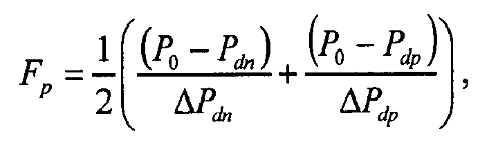
where ΔP dn and ΔP dp are the negative and positive focus offsets (in units of length). - Note that (P t - P dn )/ΔP dn and (P t - P dp )/ΔP dp model the pattern features that are lost during negative and positive defocusing, respectively. In the above example, we compute the process-sensitivity model, Fp, by adding (P t - P dn )/ΔP dn and (P t - P dp )/ΔP dp , and by dividing by 2 to normalize the process-sensitivity model. (Note that normalization is not necessary for the approach described herein to work.)
- Next, the system identifies a problem area in the mask layout using the process-sensitivity model. Specifically, the system first computes a problem indicator by convolving the process-sensitivity model with a multidimensional (e.g., 2-D) function that represents the mask layout (step 208). (Note that, for the convolution operation, the process-sensitivity model is typically represented using a 2-D function in the space domain.)
- Next, the system identifies the problem area in the mask layout by comparing the value of the problem-indicator with a threshold to identify the problem area in the mask layout (step 210).
- Note that by using appropriate off-target process models, the above described process can readily identify manufacturing problems that occur due to various mask-layout related reasons. These include, but are not limited to, 2-D effects (e.g., line-end pullback), proximity problems, jog sizing, and phase shift masks.
- FIG. 4A illustrates a 1-D plot of a problem indicator in accordance with an embodiment of the present invention. Note that although the problem indicator is typically a 2-D function, it has been illustrated in FIG. 4A as a 1-D function for the sake of clarity. The X axis corresponds to a location along a straight line in the mask layout, whereas the Y axis corresponds to the value of the problem indicator at that location.
- The value of the problem indicator 400 can be compared with one or more thresholds, such as
thresholds problem areas - Furthermore, the value of the problem indicator can indicate type and intensity of a problem. Specifically,
thresholds space problem area 410 andpolygon problem area 412 by comparing problem indicator 400 withthresholds problem areas - Similarly,
thresholds polygon problem area 414 by comparing problem indicator 400 withthreshold 406. - FIG. 4B illustrates areas in a mask layout where a problem indicator is above or below a problem threshold in accordance with an embodiment of the present invention. (Note that the mask layout is not shown for the sake of clarity.)
- Specifically, the value of the problem indicator is greater than a space problem threshold in
areas areas - FIG. 5 illustrates how a process-sensitivity model can be used to identify an area in a mask layout which is likely to cause manufacturing problems in accordance with an embodiment of the present invention. (Note that the solid lines depict the corrected mask layout, and the shaded areas depict the effective pattern.)
- A mask layout typically includes a number of patterns, such as
patterns effective pattern - In one embodiment of the present invention, the system generates a contour, such as
contour - For example,
effective pattern 506 has minimal pullback at line-end 514. As a result, the system does not generate a contour in the proximity of line-end 514. On the other hand, the amount of pullback at line-end 516 is large enough to potentially cause manufacturing problems. Accordingly, the system generatescontour 510 that clearly identifies an area in the proximity of line-end 516 to be a potential manufacturing problem area. - Similarly, the system does not generate a contour for
edge 518 because the amount of shrinkage atedge 518 is minimal. In contrast,effective pattern 508 has substantial shrinkage atedge 520. Consequently, the system generatescontour 512 that clearly identifies an area in the proximity ofedge 520 to be a potential manufacturing problem area. - Note that the system generates these contours by comparing a problem indicator with a problem threshold. Moreover, in one embodiment of the present invention, the system displays the contours using a standard optical intensity viewing tool.
- Furthermore, the system can identify problem areas in an uncorrected, partially corrected, or completely corrected mask layout. For example, the system can identify problem areas in a mask layout before an OPC process is performed on the mask layout. Specifically, in one embodiment of the present invention, the system adjusts the problem threshold to effectively compensate for the OPC on the uncorrected pattern.
- On the other hand, the system typically operates after certain resolution enhancement techniques (RETs) have been applied to the mask layout. These RETs include, but are not limited to, alternating phase shift mask, assist features, dual dipole illumination, or chromeless phase lithography (CPL).
- Note that the system can operate before an OPC process is performed because an OPC process usually does not substantially change the spatial frequency components or phase characteristics of a mask layout. On the other hand, assist features, for example, can substantially change the spatial frequency components of a mask layout. Hence, these RETs are usually performed before the system is used to identify problem areas in a mask layout.
- The data structures and code described in the foregoing description are typically stored on a computer-readable storage medium, which may be any device or medium that can store code and/or data for use by a computer system. This includes, but is not limited to, magnetic and optical storage devices such as disk drives, magnetic tape, CDs (compact discs) and DVDs (digital versatile discs or digital video discs), and computer instruction signals embodied in a transmission medium (with or without a carrier wave upon which the signals are modulated). For example, the transmission medium may include a communications network, such as the Internet.
- Furthermore, the foregoing descriptions of embodiments of the present invention have been presented only for purposes of illustration and description. They are not intended to be exhaustive or to limit the present invention to the forms disclosed. Accordingly, many modifications and variations will be readily apparent. Additionally, the above disclosure is not intended to limit the present invention. The scope of the present invention is defined by the appended claims.
Claims (22)
- A method for identifying an area in a mask layout which is likely to cause manufacturing problems, the method comprising:creating an on-target process model that models a semiconductor manufacturing process under nominal (e.g., optimal) process conditions;creating one or more off-target process models that model the semiconductor manufacturing process under one or more arbitrary (e.g., non-optimal) process conditions;computing a process-sensitivity model using the on-target process model and the one or more off-target process models, wherein the process-sensitivity model can be represented by a multidimensional function; andidentifying a problem area in the mask layout using the process-sensitivity model, wherein identifying the problem area allows it to be corrected, thereby improving the manufacturability of the mask layout;wherein using the process-sensitivity model to identify the problem area reduces the computational time required to identify the problem area.
- The method of claim 1, wherein computing the process-sensitivity model using the on-target process model and the one or more off-target process models involves subtracting each off-target process model in the one or more off-target process models from the on-target process model.
- The method of claim 1 or 2, wherein identifying the problem area in the mask layout involves:computing a problem-indicator by convolving the process-sensitivity model with a multidimensional function that represents the mask layout; andcomparing the value of the problem-indicator with a threshold to identify the problem area in the mask layout.
- The method of any preceding claim, wherein creating the on-target process model involves fitting an analytical model to process data for the semiconductor manufacturing process under nominal (e.g., optimal) process conditions;
wherein creating the one or more off-target process models involves fitting an analytical model to process data for the semiconductor manufacturing process under arbitrary (e.g., non-optimal) process conditions. - The method of any preceding claim, wherein the method is performed before an optical proximity correction (OPC) process is performed on the mask layout.
- The method of any preceding claim, wherein the semiconductor manufacturing process can include:photolithography;etch;chemical-mechanical polishing (CMP);trench fill; orreticle manufacture.
- The method of any preceding claim, wherein the method is performed after one or more resolution enhancement techniques have been applied to the mask layout, wherein the resolution enhancement techniques can include:alternating phase shift mask;assist features;dual dipole illumination; orchromeless phase lithography (CPL).
- A computer-readable storage medium storing instructions that when executed by a computer cause the computer to perform a method for identifying an area in a mask layout which is likely to cause manufacturing problems, the method comprising:creating an on-target process model that models a semiconductor manufacturing process under nominal (e.g., optimal) process conditions;creating one or more off-target process models that model the semiconductor manufacturing process under one or more arbitrary (e.g., non-optimal) process conditions;computing a process-sensitivity model using the on-target process model and the one or more off-target process models, wherein the process-sensitivity model can be represented by a multidimensional function; andidentifying a problem area in the mask layout using the process-sensitivity model, wherein identifying the problem area allows it to be corrected, thereby improving the manufacturability of the mask layout;wherein using the process-sensitivity model to identify the problem area reduces the computational time required to identify the problem area.
- The computer-readable storage medium of claim 8, wherein computing the process-sensitivity model using the on-target process model and the one or more off-target process models involves subtracting each off-target process model in the one or more off-target process models from the on-target process model.
- The computer-readable storage medium of claim 8 or 9, wherein identifying the problem area in the mask layout involves:computing a problem-indicator by convolving the process-sensitivity model with a multidimensional function that represents the mask layout; andcomparing the value of the problem-indicator with a threshold to identify the problem area in the mask layout.
- The computer-readable storage medium of any of claims 8 to 10,
wherein creating the on-target process model involves fitting an analytical model to process data for the semiconductor manufacturing process under nominal (e.g., optimal) process conditions;
wherein creating the one or more off-target process models involves fitting an analytical model to process data for the semiconductor manufacturing process under arbitrary (e.g., non-optimal) process conditions. - The computer-readable storage medium of any of claims 8 to 11,
wherein the method is performed before an optical proximity correction (OPC) process is performed on the mask layout. - The computer-readable storage medium of any of claims 8 to 12,
wherein the semiconductor manufacturing process can include:photolithography;etch;chemical-mechanical polishing (CMP);trench fill; orreticle manufacture. - The computer-readable storage medium of any of claims 8 to 13, wherein the method is performed after one or more resolution enhancement techniques have been applied to the mask layout, wherein the resolution enhancement techniques can include:alternating phase shift mask;assist features;dual dipole illumination; orchromeless phase lithography (CPL).
- A method for identifying a manufacturing problem area in an uncorrected, partially corrected, or completely corrected mask layout using a process-sensitivity model, the method comprising:computing a problem-indicator by convolving a first multidimensional function that represents the process-sensitivity model with a second multidimensional function that represents the mask layout; andidentifying the manufacturing problem area in the mask layout using the problem-indicator;wherein the first multidimensional function captures all the process-sensitivity information, thereby substantially reducing the amount of computation required for identifying the manufacturing problem area.
- The method of claim 15, wherein identifying the manufacturing problem area involves comparing the problem-indicator with one or more problem-thresholds.
- The method of claim 15 or 16, wherein convolving the first multidimensional function that represents the process-sensitivity model with the second multidimensional function that represents the mask layout involves:approximating the first multidimensional function using a set of basis functions; andconvolving the set of basis functions with the second multidimensional function.
- A method for improving the manufacturability of an uncorrected, partially corrected, or completely corrected mask layout, the method comprising:identifying a problem area in the mask layout using a process-sensitivity model which can be represented by a first multidimensional function that captures all the process-sensitivity information;wherein identifying the problem area allows it to be corrected, thereby improving the manufacturability of the mask layout.
- The method of claim 18, wherein the process-sensitivity model can be created by,
creating an on-target process model that models a semiconductor manufacturing process under nominal (e.g., optimal) process conditions;
creating one or more off-target process models that model the semiconductor manufacturing process under one or more arbitrary (e.g., non-optimal) process conditions; and
creating the process-sensitivity model using the on-target process model and the one or more off-target process models. - The method of claim 18 or 19, wherein identifying the problem area involves:convolving the process-sensitivity model with a second multidimensional function that represents the mask layout; andidentifying the problem area using the result of the convolution.
- A computer program for implementing the method of any of claims 1-7 or 15-20.
- Apparatus for implementing the method of any of claims 1-7 or 15-20.
Applications Claiming Priority (1)
| Application Number | Priority Date | Filing Date | Title |
|---|---|---|---|
| US11/065,409 US7251807B2 (en) | 2005-02-24 | 2005-02-24 | Method and apparatus for identifying a manufacturing problem area in a layout using a process-sensitivity model |
Publications (3)
| Publication Number | Publication Date |
|---|---|
| EP1696269A2 true EP1696269A2 (en) | 2006-08-30 |
| EP1696269A3 EP1696269A3 (en) | 2008-01-23 |
| EP1696269B1 EP1696269B1 (en) | 2009-09-09 |
Family
ID=35999476
Family Applications (1)
| Application Number | Title | Priority Date | Filing Date |
|---|---|---|---|
| EP06250313A Expired - Lifetime EP1696269B1 (en) | 2005-02-24 | 2006-01-20 | Identifying a problem area in a layout using a process-sensitivity model |
Country Status (9)
| Country | Link |
|---|---|
| US (4) | US7251807B2 (en) |
| EP (1) | EP1696269B1 (en) |
| JP (1) | JP4925408B2 (en) |
| KR (1) | KR101190399B1 (en) |
| CN (2) | CN1828613B (en) |
| AT (1) | ATE442610T1 (en) |
| DE (1) | DE602006009001D1 (en) |
| SG (1) | SG125169A1 (en) |
| TW (2) | TWI325547B (en) |
Cited By (6)
| Publication number | Priority date | Publication date | Assignee | Title |
|---|---|---|---|---|
| EP1862857A3 (en) * | 2006-05-31 | 2007-12-12 | Synopsys, Inc. | Method and apparatus for determining a process model for integrated circuit fabrication |
| WO2008136873A1 (en) * | 2007-05-07 | 2008-11-13 | Synopsys, Inc. | Determining a process model that models the impact of car/peb on the resist profile |
| US7454739B2 (en) | 2006-05-31 | 2008-11-18 | Synopsys, Inc. | Method and apparatus for determining an accurate photolithography process model |
| WO2009148972A1 (en) * | 2008-06-03 | 2009-12-10 | Brion Technologies, Inc. | Methods for model-based process simulation |
| WO2010044946A1 (en) * | 2008-10-13 | 2010-04-22 | Synopsys, Inc. | Method and apparatus for determining a photolithography process model which models the influence of topography variations |
| US8443307B2 (en) | 2008-11-10 | 2013-05-14 | Asml Netherlands B.V. | Methods and system for model-based generic matching and tuning |
Families Citing this family (31)
| Publication number | Priority date | Publication date | Assignee | Title |
|---|---|---|---|---|
| US7251807B2 (en) * | 2005-02-24 | 2007-07-31 | Synopsys, Inc. | Method and apparatus for identifying a manufacturing problem area in a layout using a process-sensitivity model |
| US7475382B2 (en) * | 2005-02-24 | 2009-01-06 | Synopsys, Inc. | Method and apparatus for determining an improved assist feature configuration in a mask layout |
| US7315999B2 (en) * | 2005-03-17 | 2008-01-01 | Synopsys, Inc. | Method and apparatus for identifying assist feature placement problems |
| US7496880B2 (en) * | 2005-03-17 | 2009-02-24 | Synopsys, Inc. | Method and apparatus for assessing the quality of a process model |
| US7458059B2 (en) * | 2005-10-31 | 2008-11-25 | Synopsys, Inc. | Model of sensitivity of a simulated layout to a change in original layout, and use of model in proximity correction |
| US7840287B2 (en) * | 2006-04-13 | 2010-11-23 | Fisher-Rosemount Systems, Inc. | Robust process model identification in model based control techniques |
| US20100205573A1 (en) * | 2007-07-06 | 2010-08-12 | Sagantiec Israel Ltd. | Layout modification engine for modifying a circuit layout comprising fixed and free layout entities |
| TW200929412A (en) * | 2007-12-18 | 2009-07-01 | Airoha Tech Corp | Model modification method for a semiconductor device |
| US8120767B2 (en) * | 2008-03-13 | 2012-02-21 | Taiwan Semiconductor Manufacturing Company, Ltd. | Mask making decision for manufacturing (DFM) on mask quality control |
| JP2009282319A (en) * | 2008-05-22 | 2009-12-03 | Toshiba Corp | Pattern verification method, pattern verification system, pattern verification program, method for manufacturing mask, and method for manufacturing semiconductor device |
| US8117568B2 (en) * | 2008-09-25 | 2012-02-14 | International Business Machines Corporation | Apparatus, method and computer program product for fast simulation of manufacturing effects during integrated circuit design |
| JP4762288B2 (en) * | 2008-09-26 | 2011-08-31 | 株式会社東芝 | Pattern formation defective area calculation method |
| US7954071B2 (en) * | 2008-10-31 | 2011-05-31 | Synopsys, Inc. | Assist feature placement based on a focus-sensitive cost-covariance field |
| US8136054B2 (en) * | 2009-01-29 | 2012-03-13 | Synopsys, Inc. | Compact abbe's kernel generation using principal component analysis |
| US8010913B2 (en) * | 2009-04-14 | 2011-08-30 | Synopsys, Inc. | Model-based assist feature placement using inverse imaging approach |
| US9448706B2 (en) * | 2009-07-29 | 2016-09-20 | Synopsys, Inc. | Loop removal in electronic design automation |
| US8694930B2 (en) * | 2011-08-11 | 2014-04-08 | Infineon Technologies Ag | Method and apparatus for providing a layout defining a structure to be patterned onto a substrate |
| US8510699B1 (en) | 2012-03-09 | 2013-08-13 | International Business Machines Corporation | Performance driven layout optimization using morphing of a basis set of representative layouts |
| US10365557B2 (en) * | 2013-02-24 | 2019-07-30 | Synopsys, Inc. | Compact OPC model generation using virtual data |
| TWI621957B (en) * | 2013-03-14 | 2018-04-21 | 新納普系統股份有限公司 | Sub-resolution assist feature implementation using shot optimization |
| CN103405164B (en) * | 2013-07-23 | 2015-08-12 | 山东科技大学 | Baking box coordinates the method for layout with baking tray |
| JP6346297B2 (en) * | 2014-02-11 | 2018-06-20 | エーエスエムエル ネザーランズ ビー.ブイ. | A model for calculating stochastic variations in arbitrary patterns |
| EP2952964A1 (en) * | 2014-06-03 | 2015-12-09 | Aselta Nanographics | Method for determining the parameters of an ic manufacturing process by a differential procedure |
| WO2016008711A1 (en) | 2014-07-14 | 2016-01-21 | Asml Netherlands B.V. | Optimization of assist features and source |
| KR102084048B1 (en) * | 2014-10-02 | 2020-03-03 | 에이에스엠엘 네델란즈 비.브이. | Rule-based deployment of assist features |
| KR102028712B1 (en) | 2015-04-10 | 2019-10-04 | 에이에스엠엘 네델란즈 비.브이. | Method and apparatus for inspection and measurement |
| US10394116B2 (en) | 2017-09-06 | 2019-08-27 | International Business Machines Corporation | Semiconductor fabrication design rule loophole checking for design for manufacturability optimization |
| US10621295B2 (en) | 2018-04-10 | 2020-04-14 | International Business Machines Corporation | Incorporation of process variation contours in design rule and risk estimation aspects of design for manufacturability to increase fabrication yield |
| CN109596638B (en) * | 2018-10-26 | 2022-05-06 | 中国科学院光电研究院 | Method and apparatus for defect detection of patterned wafer and reticle |
| CN112904662B (en) * | 2021-05-07 | 2021-07-23 | 南京晶驱集成电路有限公司 | Auxiliary graph adding method and device and test layout |
| CN114509912B (en) * | 2022-01-07 | 2026-04-28 | 东方晶源微电子科技(北京)股份有限公司 | A mask optimization method, a mask optimization device, and an electronic device. |
Family Cites Families (25)
| Publication number | Priority date | Publication date | Assignee | Title |
|---|---|---|---|---|
| JPS6474547A (en) | 1987-09-14 | 1989-03-20 | Motorola Inc | Manufacture of semiconductor for compensating strain between pattern on semiconductor body and mask for obtaining pattern |
| JPH04216548A (en) * | 1990-12-18 | 1992-08-06 | Mitsubishi Electric Corp | Photomask |
| JP3223718B2 (en) * | 1994-09-07 | 2001-10-29 | 松下電器産業株式会社 | How to create mask data |
| US5774177A (en) * | 1996-09-11 | 1998-06-30 | Milliken Research Corporation | Textile fabric inspection system |
| US5965309A (en) * | 1997-08-28 | 1999-10-12 | International Business Machines Corporation | Focus or exposure dose parameter control system using tone reversing patterns |
| US6183919B1 (en) * | 1999-06-11 | 2001-02-06 | International Business Machines Corporation | Darkfield imaging for enhancing optical detection of edges and minimum features |
| US6539521B1 (en) * | 2000-09-29 | 2003-03-25 | Numerical Technologies, Inc. | Dissection of corners in a fabrication layout for correcting proximity effects |
| US6453457B1 (en) * | 2000-09-29 | 2002-09-17 | Numerical Technologies, Inc. | Selection of evaluation point locations based on proximity effects model amplitudes for correcting proximity effects in a fabrication layout |
| AU2002238409A1 (en) * | 2000-11-30 | 2002-06-11 | Sigma-C Gmbh | Method and device for determining the properties of an integrated circuit |
| US6873720B2 (en) * | 2001-03-20 | 2005-03-29 | Synopsys, Inc. | System and method of providing mask defect printability analysis |
| JP4748343B2 (en) * | 2001-04-26 | 2011-08-17 | 大日本印刷株式会社 | Wafer transcription verification method |
| TW520544B (en) * | 2001-06-15 | 2003-02-11 | United Microelectronics Corp | Method and apparatus for measuring bridge caused by mask layout correction |
| DE10143723B4 (en) * | 2001-08-31 | 2006-09-28 | Infineon Technologies Ag | A method for optimizing a layout for a mask for use in semiconductor fabrication |
| US6673638B1 (en) * | 2001-11-14 | 2004-01-06 | Kla-Tencor Corporation | Method and apparatus for the production of process sensitive lithographic features |
| US20030121021A1 (en) * | 2001-12-26 | 2003-06-26 | Numerical Technologies, Inc. | System and method for determining manufacturing error enhancement factor |
| US6904587B2 (en) * | 2002-12-20 | 2005-06-07 | Synopsys, Inc. | Incremental lithography mask layout design and verification |
| US6964032B2 (en) * | 2003-02-28 | 2005-11-08 | International Business Machines Corporation | Pitch-based subresolution assist feature design |
| US6934930B2 (en) * | 2003-07-08 | 2005-08-23 | Texas Instruments Incorporated | Generating an optical model for lens aberrations |
| JP4684584B2 (en) * | 2003-07-23 | 2011-05-18 | キヤノン株式会社 | Mask, manufacturing method thereof, and exposure method |
| JP2005099765A (en) * | 2003-08-28 | 2005-04-14 | Toshiba Corp | Method for generating predictive model for process proximity effect, method for managing process, method for manufacturing semiconductor device, method for manufacturing photomask, and program |
| US6978438B1 (en) * | 2003-10-01 | 2005-12-20 | Advanced Micro Devices, Inc. | Optical proximity correction (OPC) technique using generalized figure of merit for photolithograhic processing |
| US7451068B2 (en) * | 2003-10-10 | 2008-11-11 | Synopsys, Inc. | Method and apparatus for generating an OPC segmentation based on modeled intensity gradients |
| US7251807B2 (en) * | 2005-02-24 | 2007-07-31 | Synopsys, Inc. | Method and apparatus for identifying a manufacturing problem area in a layout using a process-sensitivity model |
| US7475382B2 (en) * | 2005-02-24 | 2009-01-06 | Synopsys, Inc. | Method and apparatus for determining an improved assist feature configuration in a mask layout |
| US7315999B2 (en) * | 2005-03-17 | 2008-01-01 | Synopsys, Inc. | Method and apparatus for identifying assist feature placement problems |
-
2005
- 2005-02-24 US US11/065,409 patent/US7251807B2/en not_active Expired - Lifetime
- 2005-03-17 US US11/083,656 patent/US7243332B2/en not_active Expired - Fee Related
- 2005-05-06 US US11/124,328 patent/US7320119B2/en not_active Expired - Lifetime
- 2005-12-27 SG SG200508409A patent/SG125169A1/en unknown
- 2005-12-28 TW TW094147031A patent/TWI325547B/en not_active IP Right Cessation
- 2005-12-28 TW TW098143909A patent/TWI450115B/en not_active IP Right Cessation
-
2006
- 2006-01-10 CN CN2006100012292A patent/CN1828613B/en not_active Expired - Lifetime
- 2006-01-11 JP JP2006004222A patent/JP4925408B2/en not_active Expired - Lifetime
- 2006-01-20 DE DE602006009001T patent/DE602006009001D1/en not_active Expired - Lifetime
- 2006-01-20 EP EP06250313A patent/EP1696269B1/en not_active Expired - Lifetime
- 2006-01-20 AT AT06250313T patent/ATE442610T1/en not_active IP Right Cessation
- 2006-01-24 CN CNB2006100015924A patent/CN100541498C/en not_active Expired - Lifetime
- 2006-02-20 KR KR1020060016042A patent/KR101190399B1/en not_active Expired - Lifetime
-
2007
- 2007-05-08 US US11/801,350 patent/US7784018B2/en active Active
Cited By (19)
| Publication number | Priority date | Publication date | Assignee | Title |
|---|---|---|---|---|
| US7454739B2 (en) | 2006-05-31 | 2008-11-18 | Synopsys, Inc. | Method and apparatus for determining an accurate photolithography process model |
| EP1862857A3 (en) * | 2006-05-31 | 2007-12-12 | Synopsys, Inc. | Method and apparatus for determining a process model for integrated circuit fabrication |
| US7743357B2 (en) | 2006-05-31 | 2010-06-22 | Synopsys, Inc. | Method and apparatus for determining a process model that models the impact of CAR/PEB on the resist profile |
| US7934176B2 (en) | 2007-05-07 | 2011-04-26 | Synopsys, Inc. | Method and apparatus for determining a process model that models the impact of a CAR/PEB on the resist profile |
| WO2008136873A1 (en) * | 2007-05-07 | 2008-11-13 | Synopsys, Inc. | Determining a process model that models the impact of car/peb on the resist profile |
| TWI425376B (en) * | 2007-05-07 | 2014-02-01 | Synopsys Inc | Method and apparatus for determining a process model that models the impact of car/peb on the resist profile |
| WO2009148972A1 (en) * | 2008-06-03 | 2009-12-10 | Brion Technologies, Inc. | Methods for model-based process simulation |
| CN102057329A (en) * | 2008-06-03 | 2011-05-11 | Asml荷兰有限公司 | Methods for model-based process simulation |
| US10569469B2 (en) | 2008-06-03 | 2020-02-25 | Asml Netherlands B.V. | Model-based scanner tuning systems and methods |
| US10137643B2 (en) | 2008-06-03 | 2018-11-27 | Asml Netherlands B.V. | Model-based process simulation systems and methods |
| CN102057329B (en) * | 2008-06-03 | 2013-08-21 | Asml荷兰有限公司 | Methods for model-based process simulation |
| US8571845B2 (en) | 2008-06-03 | 2013-10-29 | Asml Netherlands B.V. | Model-based scanner tuning systems and methods |
| US8874423B2 (en) | 2008-06-03 | 2014-10-28 | Asml Netherlands B.V. | Model-based scanner tuning systems and methods |
| US8806387B2 (en) | 2008-06-03 | 2014-08-12 | Asml Netherlands B.V. | Model-based process simulation systems and methods |
| WO2010044946A1 (en) * | 2008-10-13 | 2010-04-22 | Synopsys, Inc. | Method and apparatus for determining a photolithography process model which models the influence of topography variations |
| US8181128B2 (en) | 2008-10-13 | 2012-05-15 | Synopsys, Inc. | Method and apparatus for determining a photolithography process model which models the influence of topography variations |
| US8893058B2 (en) | 2008-11-10 | 2014-11-18 | Asml Netherlands B.V. | Methods and system for model-based generic matching and tuning |
| US8443307B2 (en) | 2008-11-10 | 2013-05-14 | Asml Netherlands B.V. | Methods and system for model-based generic matching and tuning |
| US10169522B2 (en) | 2008-11-10 | 2019-01-01 | Asml Netherlands B.V. | Methods and system for model-based generic matching and tuning |
Also Published As
| Publication number | Publication date |
|---|---|
| US20060190914A1 (en) | 2006-08-24 |
| US7243332B2 (en) | 2007-07-10 |
| US7251807B2 (en) | 2007-07-31 |
| KR20060094470A (en) | 2006-08-29 |
| EP1696269B1 (en) | 2009-09-09 |
| US7784018B2 (en) | 2010-08-24 |
| TWI325547B (en) | 2010-06-01 |
| KR101190399B1 (en) | 2012-10-12 |
| CN1825323A (en) | 2006-08-30 |
| DE602006009001D1 (en) | 2009-10-22 |
| US7320119B2 (en) | 2008-01-15 |
| CN100541498C (en) | 2009-09-16 |
| CN1828613B (en) | 2011-05-18 |
| JP4925408B2 (en) | 2012-04-25 |
| TWI450115B (en) | 2014-08-21 |
| EP1696269A3 (en) | 2008-01-23 |
| US20070250804A1 (en) | 2007-10-25 |
| TW201017460A (en) | 2010-05-01 |
| TW200639668A (en) | 2006-11-16 |
| US20060190913A1 (en) | 2006-08-24 |
| JP2006235600A (en) | 2006-09-07 |
| SG125169A1 (en) | 2006-09-29 |
| ATE442610T1 (en) | 2009-09-15 |
| US20060190912A1 (en) | 2006-08-24 |
| CN1828613A (en) | 2006-09-06 |
Similar Documents
| Publication | Publication Date | Title |
|---|---|---|
| US7251807B2 (en) | Method and apparatus for identifying a manufacturing problem area in a layout using a process-sensitivity model | |
| US7475382B2 (en) | Method and apparatus for determining an improved assist feature configuration in a mask layout | |
| US7421678B2 (en) | Assist feature placement using a process-sensitivity model | |
| EP1677221B1 (en) | Method and apparatus for placing assist features in a layout | |
| US20070038973A1 (en) | Method and apparatus for quickly determining the effect of placing an assist feature at a location in a layout | |
| US7739651B2 (en) | Method and apparatus to determine if a pattern is robustly manufacturable | |
| US20060110837A1 (en) | Method and system for topography-aware reticle enhancement | |
| US7315999B2 (en) | Method and apparatus for identifying assist feature placement problems | |
| US7207029B2 (en) | Calculating etch proximity-correction using image-precision techniques | |
| US7234129B2 (en) | Calculating etch proximity-correction using object-precision techniques | |
| US7313774B2 (en) | Method and apparatus for associating an error in a layout with a cell | |
| Kim et al. | Process capability analysis of DUV alternating PSM and DUV attenuated PSM lithography for 100-nm gate fabrication | |
| Kim et al. | Model-based full-chip verification for 65nm lithography process development | |
| Zhang et al. | Model-based lithography verification using the new manufacturing sensitivity model | |
| Melvin III et al. | 12, Patent Application Publication o Pub. No.: US 2006/0206854A1 | |
| Belova et al. | Simple method for restricting OPC model minimum spacing and width for a no-failure imaging solution |
Legal Events
| Date | Code | Title | Description |
|---|---|---|---|
| PUAI | Public reference made under article 153(3) epc to a published international application that has entered the european phase |
Free format text: ORIGINAL CODE: 0009012 |
|
| AK | Designated contracting states |
Kind code of ref document: A2 Designated state(s): AT BE BG CH CY CZ DE DK EE ES FI FR GB GR HU IE IS IT LI LT LU LV MC NL PL PT RO SE SI SK TR |
|
| AX | Request for extension of the european patent |
Extension state: AL BA HR MK YU |
|
| PUAL | Search report despatched |
Free format text: ORIGINAL CODE: 0009013 |
|
| AK | Designated contracting states |
Kind code of ref document: A3 Designated state(s): AT BE BG CH CY CZ DE DK EE ES FI FR GB GR HU IE IS IT LI LT LU LV MC NL PL PT RO SE SI SK TR |
|
| AX | Request for extension of the european patent |
Extension state: AL BA HR MK YU |
|
| RIC1 | Information provided on ipc code assigned before grant |
Ipc: G03F 1/14 20060101ALI20071218BHEP Ipc: G03F 7/20 20060101AFI20060329BHEP |
|
| 17P | Request for examination filed |
Effective date: 20080331 |
|
| 17Q | First examination report despatched |
Effective date: 20080611 |
|
| AKX | Designation fees paid |
Designated state(s): AT BE BG CH CY CZ DE DK EE ES FI FR GB GR HU IE IS IT LI LT LU LV MC NL PL PT RO SE SI SK TR |
|
| GRAP | Despatch of communication of intention to grant a patent |
Free format text: ORIGINAL CODE: EPIDOSNIGR1 |
|
| GRAS | Grant fee paid |
Free format text: ORIGINAL CODE: EPIDOSNIGR3 |
|
| GRAA | (expected) grant |
Free format text: ORIGINAL CODE: 0009210 |
|
| AK | Designated contracting states |
Kind code of ref document: B1 Designated state(s): AT BE BG CH CY CZ DE DK EE ES FI FR GB GR HU IE IS IT LI LT LU LV MC NL PL PT RO SE SI SK TR |
|
| REG | Reference to a national code |
Ref country code: GB Ref legal event code: FG4D |
|
| REG | Reference to a national code |
Ref country code: CH Ref legal event code: EP |
|
| REG | Reference to a national code |
Ref country code: IE Ref legal event code: FG4D |
|
| REF | Corresponds to: |
Ref document number: 602006009001 Country of ref document: DE Date of ref document: 20091022 Kind code of ref document: P |
|
| PG25 | Lapsed in a contracting state [announced via postgrant information from national office to epo] |
Ref country code: LT Free format text: LAPSE BECAUSE OF FAILURE TO SUBMIT A TRANSLATION OF THE DESCRIPTION OR TO PAY THE FEE WITHIN THE PRESCRIBED TIME-LIMIT Effective date: 20090909 Ref country code: FI Free format text: LAPSE BECAUSE OF FAILURE TO SUBMIT A TRANSLATION OF THE DESCRIPTION OR TO PAY THE FEE WITHIN THE PRESCRIBED TIME-LIMIT Effective date: 20090909 Ref country code: SE Free format text: LAPSE BECAUSE OF FAILURE TO SUBMIT A TRANSLATION OF THE DESCRIPTION OR TO PAY THE FEE WITHIN THE PRESCRIBED TIME-LIMIT Effective date: 20090909 |
|
| NLV1 | Nl: lapsed or annulled due to failure to fulfill the requirements of art. 29p and 29m of the patents act | ||
| LTIE | Lt: invalidation of european patent or patent extension |
Effective date: 20090909 |
|
| PG25 | Lapsed in a contracting state [announced via postgrant information from national office to epo] |
Ref country code: PL Free format text: LAPSE BECAUSE OF FAILURE TO SUBMIT A TRANSLATION OF THE DESCRIPTION OR TO PAY THE FEE WITHIN THE PRESCRIBED TIME-LIMIT Effective date: 20090909 Ref country code: NL Free format text: LAPSE BECAUSE OF FAILURE TO SUBMIT A TRANSLATION OF THE DESCRIPTION OR TO PAY THE FEE WITHIN THE PRESCRIBED TIME-LIMIT Effective date: 20090909 Ref country code: SI Free format text: LAPSE BECAUSE OF FAILURE TO SUBMIT A TRANSLATION OF THE DESCRIPTION OR TO PAY THE FEE WITHIN THE PRESCRIBED TIME-LIMIT Effective date: 20090909 Ref country code: LV Free format text: LAPSE BECAUSE OF FAILURE TO SUBMIT A TRANSLATION OF THE DESCRIPTION OR TO PAY THE FEE WITHIN THE PRESCRIBED TIME-LIMIT Effective date: 20090909 |
|
| PG25 | Lapsed in a contracting state [announced via postgrant information from national office to epo] |
Ref country code: CY Free format text: LAPSE BECAUSE OF FAILURE TO SUBMIT A TRANSLATION OF THE DESCRIPTION OR TO PAY THE FEE WITHIN THE PRESCRIBED TIME-LIMIT Effective date: 20090909 |
|
| PG25 | Lapsed in a contracting state [announced via postgrant information from national office to epo] |
Ref country code: RO Free format text: LAPSE BECAUSE OF FAILURE TO SUBMIT A TRANSLATION OF THE DESCRIPTION OR TO PAY THE FEE WITHIN THE PRESCRIBED TIME-LIMIT Effective date: 20090909 Ref country code: ES Free format text: LAPSE BECAUSE OF FAILURE TO SUBMIT A TRANSLATION OF THE DESCRIPTION OR TO PAY THE FEE WITHIN THE PRESCRIBED TIME-LIMIT Effective date: 20091220 Ref country code: EE Free format text: LAPSE BECAUSE OF FAILURE TO SUBMIT A TRANSLATION OF THE DESCRIPTION OR TO PAY THE FEE WITHIN THE PRESCRIBED TIME-LIMIT Effective date: 20090909 Ref country code: PT Free format text: LAPSE BECAUSE OF FAILURE TO SUBMIT A TRANSLATION OF THE DESCRIPTION OR TO PAY THE FEE WITHIN THE PRESCRIBED TIME-LIMIT Effective date: 20100111 Ref country code: CZ Free format text: LAPSE BECAUSE OF FAILURE TO SUBMIT A TRANSLATION OF THE DESCRIPTION OR TO PAY THE FEE WITHIN THE PRESCRIBED TIME-LIMIT Effective date: 20090909 Ref country code: IS Free format text: LAPSE BECAUSE OF FAILURE TO SUBMIT A TRANSLATION OF THE DESCRIPTION OR TO PAY THE FEE WITHIN THE PRESCRIBED TIME-LIMIT Effective date: 20100109 |
|
| PG25 | Lapsed in a contracting state [announced via postgrant information from national office to epo] |
Ref country code: SK Free format text: LAPSE BECAUSE OF FAILURE TO SUBMIT A TRANSLATION OF THE DESCRIPTION OR TO PAY THE FEE WITHIN THE PRESCRIBED TIME-LIMIT Effective date: 20090909 |
|
| PG25 | Lapsed in a contracting state [announced via postgrant information from national office to epo] |
Ref country code: BE Free format text: LAPSE BECAUSE OF FAILURE TO SUBMIT A TRANSLATION OF THE DESCRIPTION OR TO PAY THE FEE WITHIN THE PRESCRIBED TIME-LIMIT Effective date: 20090909 Ref country code: AT Free format text: LAPSE BECAUSE OF FAILURE TO SUBMIT A TRANSLATION OF THE DESCRIPTION OR TO PAY THE FEE WITHIN THE PRESCRIBED TIME-LIMIT Effective date: 20090909 |
|
| PLBE | No opposition filed within time limit |
Free format text: ORIGINAL CODE: 0009261 |
|
| STAA | Information on the status of an ep patent application or granted ep patent |
Free format text: STATUS: NO OPPOSITION FILED WITHIN TIME LIMIT |
|
| PG25 | Lapsed in a contracting state [announced via postgrant information from national office to epo] |
Ref country code: DK Free format text: LAPSE BECAUSE OF FAILURE TO SUBMIT A TRANSLATION OF THE DESCRIPTION OR TO PAY THE FEE WITHIN THE PRESCRIBED TIME-LIMIT Effective date: 20090909 |
|
| 26N | No opposition filed |
Effective date: 20100610 |
|
| PG25 | Lapsed in a contracting state [announced via postgrant information from national office to epo] |
Ref country code: MC Free format text: LAPSE BECAUSE OF NON-PAYMENT OF DUE FEES Effective date: 20100131 |
|
| REG | Reference to a national code |
Ref country code: CH Ref legal event code: PL |
|
| PG25 | Lapsed in a contracting state [announced via postgrant information from national office to epo] |
Ref country code: CH Free format text: LAPSE BECAUSE OF NON-PAYMENT OF DUE FEES Effective date: 20100131 Ref country code: GR Free format text: LAPSE BECAUSE OF FAILURE TO SUBMIT A TRANSLATION OF THE DESCRIPTION OR TO PAY THE FEE WITHIN THE PRESCRIBED TIME-LIMIT Effective date: 20091210 Ref country code: LI Free format text: LAPSE BECAUSE OF NON-PAYMENT OF DUE FEES Effective date: 20100131 |
|
| PG25 | Lapsed in a contracting state [announced via postgrant information from national office to epo] |
Ref country code: IE Free format text: LAPSE BECAUSE OF NON-PAYMENT OF DUE FEES Effective date: 20100120 |
|
| PG25 | Lapsed in a contracting state [announced via postgrant information from national office to epo] |
Ref country code: IT Free format text: LAPSE BECAUSE OF FAILURE TO SUBMIT A TRANSLATION OF THE DESCRIPTION OR TO PAY THE FEE WITHIN THE PRESCRIBED TIME-LIMIT Effective date: 20090909 |
|
| PG25 | Lapsed in a contracting state [announced via postgrant information from national office to epo] |
Ref country code: LU Free format text: LAPSE BECAUSE OF NON-PAYMENT OF DUE FEES Effective date: 20100120 Ref country code: BG Free format text: LAPSE BECAUSE OF FAILURE TO SUBMIT A TRANSLATION OF THE DESCRIPTION OR TO PAY THE FEE WITHIN THE PRESCRIBED TIME-LIMIT Effective date: 20090909 Ref country code: HU Free format text: LAPSE BECAUSE OF FAILURE TO SUBMIT A TRANSLATION OF THE DESCRIPTION OR TO PAY THE FEE WITHIN THE PRESCRIBED TIME-LIMIT Effective date: 20100310 |
|
| PG25 | Lapsed in a contracting state [announced via postgrant information from national office to epo] |
Ref country code: TR Free format text: LAPSE BECAUSE OF FAILURE TO SUBMIT A TRANSLATION OF THE DESCRIPTION OR TO PAY THE FEE WITHIN THE PRESCRIBED TIME-LIMIT Effective date: 20090909 |
|
| REG | Reference to a national code |
Ref country code: FR Ref legal event code: PLFP Year of fee payment: 11 |
|
| REG | Reference to a national code |
Ref country code: FR Ref legal event code: PLFP Year of fee payment: 12 |
|
| REG | Reference to a national code |
Ref country code: FR Ref legal event code: PLFP Year of fee payment: 13 |
|
| P01 | Opt-out of the competence of the unified patent court (upc) registered |
Effective date: 20230528 |
|
| PGFP | Annual fee paid to national office [announced via postgrant information from national office to epo] |
Ref country code: GB Payment date: 20241219 Year of fee payment: 20 |
|
| PGFP | Annual fee paid to national office [announced via postgrant information from national office to epo] |
Ref country code: FR Payment date: 20241219 Year of fee payment: 20 |
|
| PGFP | Annual fee paid to national office [announced via postgrant information from national office to epo] |
Ref country code: DE Payment date: 20241218 Year of fee payment: 20 |
|
| REG | Reference to a national code |
Ref country code: DE Ref legal event code: R071 Ref document number: 602006009001 Country of ref document: DE |
|
| REG | Reference to a national code |
Ref country code: GB Ref legal event code: PE20 Expiry date: 20260119 |