EP1695398B1 - Method and apparatus for forming patterned coated films - Google Patents
Method and apparatus for forming patterned coated films Download PDFInfo
- Publication number
- EP1695398B1 EP1695398B1 EP04810440A EP04810440A EP1695398B1 EP 1695398 B1 EP1695398 B1 EP 1695398B1 EP 04810440 A EP04810440 A EP 04810440A EP 04810440 A EP04810440 A EP 04810440A EP 1695398 B1 EP1695398 B1 EP 1695398B1
- Authority
- EP
- European Patent Office
- Prior art keywords
- coating
- electro
- wiping head
- wiping
- luminescent
- Prior art date
- Legal status (The legal status is an assumption and is not a legal conclusion. Google has not performed a legal analysis and makes no representation as to the accuracy of the status listed.)
- Expired - Lifetime
Links
Images


Classifications
-
- H—ELECTRICITY
- H10—SEMICONDUCTOR DEVICES; ELECTRIC SOLID-STATE DEVICES NOT OTHERWISE PROVIDED FOR
- H10K—ORGANIC ELECTRIC SOLID-STATE DEVICES
- H10K71/00—Manufacture or treatment specially adapted for the organic devices covered by this subclass
- H10K71/20—Changing the shape of the active layer in the devices, e.g. patterning
-
- H—ELECTRICITY
- H05—ELECTRIC TECHNIQUES NOT OTHERWISE PROVIDED FOR
- H05B—ELECTRIC HEATING; ELECTRIC LIGHT SOURCES NOT OTHERWISE PROVIDED FOR; CIRCUIT ARRANGEMENTS FOR ELECTRIC LIGHT SOURCES, IN GENERAL
- H05B33/00—Electroluminescent light sources
- H05B33/10—Apparatus or processes specially adapted to the manufacture of electroluminescent light sources
-
- H—ELECTRICITY
- H10—SEMICONDUCTOR DEVICES; ELECTRIC SOLID-STATE DEVICES NOT OTHERWISE PROVIDED FOR
- H10K—ORGANIC ELECTRIC SOLID-STATE DEVICES
- H10K71/00—Manufacture or treatment specially adapted for the organic devices covered by this subclass
- H10K71/20—Changing the shape of the active layer in the devices, e.g. patterning
- H10K71/231—Changing the shape of the active layer in the devices, e.g. patterning by etching of existing layers
-
- H—ELECTRICITY
- H10—SEMICONDUCTOR DEVICES; ELECTRIC SOLID-STATE DEVICES NOT OTHERWISE PROVIDED FOR
- H10K—ORGANIC ELECTRIC SOLID-STATE DEVICES
- H10K71/00—Manufacture or treatment specially adapted for the organic devices covered by this subclass
- H10K71/40—Thermal treatment, e.g. annealing in the presence of a solvent vapour
-
- H—ELECTRICITY
- H10—SEMICONDUCTOR DEVICES; ELECTRIC SOLID-STATE DEVICES NOT OTHERWISE PROVIDED FOR
- H10K—ORGANIC ELECTRIC SOLID-STATE DEVICES
- H10K71/00—Manufacture or treatment specially adapted for the organic devices covered by this subclass
-
- H—ELECTRICITY
- H10—SEMICONDUCTOR DEVICES; ELECTRIC SOLID-STATE DEVICES NOT OTHERWISE PROVIDED FOR
- H10K—ORGANIC ELECTRIC SOLID-STATE DEVICES
- H10K85/00—Organic materials used in the body or electrodes of devices covered by this subclass
- H10K85/10—Organic polymers or oligomers
- H10K85/111—Organic polymers or oligomers comprising aromatic, heteroaromatic, or aryl chains, e.g. polyaniline, polyphenylene or polyphenylene vinylene
- H10K85/113—Heteroaromatic compounds comprising sulfur or selene, e.g. polythiophene
- H10K85/1135—Polyethylene dioxythiophene [PEDOT]; Derivatives thereof
-
- Y—GENERAL TAGGING OF NEW TECHNOLOGICAL DEVELOPMENTS; GENERAL TAGGING OF CROSS-SECTIONAL TECHNOLOGIES SPANNING OVER SEVERAL SECTIONS OF THE IPC; TECHNICAL SUBJECTS COVERED BY FORMER USPC CROSS-REFERENCE ART COLLECTIONS [XRACs] AND DIGESTS
- Y02—TECHNOLOGIES OR APPLICATIONS FOR MITIGATION OR ADAPTATION AGAINST CLIMATE CHANGE
- Y02E—REDUCTION OF GREENHOUSE GAS [GHG] EMISSIONS, RELATED TO ENERGY GENERATION, TRANSMISSION OR DISTRIBUTION
- Y02E10/00—Energy generation through renewable energy sources
- Y02E10/50—Photovoltaic [PV] energy
- Y02E10/549—Organic PV cells
-
- Y—GENERAL TAGGING OF NEW TECHNOLOGICAL DEVELOPMENTS; GENERAL TAGGING OF CROSS-SECTIONAL TECHNOLOGIES SPANNING OVER SEVERAL SECTIONS OF THE IPC; TECHNICAL SUBJECTS COVERED BY FORMER USPC CROSS-REFERENCE ART COLLECTIONS [XRACs] AND DIGESTS
- Y10—TECHNICAL SUBJECTS COVERED BY FORMER USPC
- Y10T—TECHNICAL SUBJECTS COVERED BY FORMER US CLASSIFICATION
- Y10T428/00—Stock material or miscellaneous articles
- Y10T428/24—Structurally defined web or sheet [e.g., overall dimension, etc.]
- Y10T428/24802—Discontinuous or differential coating, impregnation or bond [e.g., artwork, printing, retouched photograph, etc.]
- Y10T428/24851—Intermediate layer is discontinuous or differential
Definitions
- This invention relates to a method of uniformly patterning an electro-luminescent layer of electro-luminescent devices.
- Electro-active devices such as organic light emitting diodes (referred hereinafter to as “OLEDs”), are widely used in organic transistors, fuel cell components, microelectronics processing, microanalytical test procedures, and in specialty electronics.
- OLEDs organic light emitting diodes
- One of the features of such devices is an electro-luminescent layer, formed from photo-sensitive materials, that emits light on receiving an electrical impulse.
- the electro-luminescent layer In order to facilitate miniaturization, conform to device geometry, and maximize electro-luminescent yield, the electro-luminescent layer must often be patterned to various textures, topography, and geometries.
- Electro-luminescent layer patterning has been conventionally performed using stamping or laser ablation.
- stamping a pattern is imprinted upon the layer using mechanical force upon a patterned die or a stamping head, whereas in laser ablation, a patterned photomask covers the area to be patterned while the remaining area is selectively etched using a laser beam.
- stamping leaves behind a substantial amount of material residue on the layer surface. Patterning by stamping also does not guarantee uniform, reproducible, and precise patterning over large specimens. While laser ablation may yield uniform, reproducible, and precisely patterned surfaces, the process needs high vacuum conditions, produces excessive debris around the patterned area, is expensive, and cannot be performed on large specimens or in fieldwork.
- EP-1351303 discloses an organic light emitting display device for displaying selected images from a plurality of images, each with one or more desired colors and also describes a method of fabrication.
- US-2002/0158295 describes an electrochemical transit device comprising a source contact, a drain contact and at least one gate electrode.
- the deposited layers may be structured by subtractive techniques such as scratching, scaring or scraping.
- displays incorporating such devices and processes for the production of such devices.
- the current methods for patterning an electro-luminescent layer in electro-active devices use mechanical or laser-beam techniques that do not enable patterned surfaces to be patterned to precision in minimal turnaround times. Therefore, what is needed is an electro-active device having an electro-luminescent layer that is precisely and quickly patterned to uniform thickness. What is also needed is a method for patterning such an electro-luminescent layer that is applicable to a variety of material compositions with a variety of solvating species. What is also needed is a patterning method that is effectively independent of the processing or forming history of the electro-luminescent film.
- the present invention meets these and other needs by providing a patterned electro-luminescent layer of substantially uniform thickness and a method and apparatus for forming patterned electro-luminescent layer of substantially uniform thickness on a continuous electroluminescent film. Different kinds of electro-luminescent layers can be patterned by this method.
- the invention also includes an apparatus for making an electro-luminescent layer by selectively removing at least one coating from a surface of a substrate.
- a method of selectively removing at least one coating from a surface of a continuous electroluminescent film comprising the steps of a) providing the electroluminescent film, the electroluminescent film having the at least one coating disposed on the surface; and b) contacting a portion of the at least one coating with a coating removing means; wherein c) said coating removing means comprises a wiping head which has solvents for solvating the electroluminescent film; and wherein said method of selectively removing at least one coating comprises d) wiping the portion with the wiping head in a direction that is tangential to the surface to remove the portion of the at least one coating from the substrate.
- the least one coating may be a wet or dry coating.
- the at least one coating may have been baked onto the surface of electroluminescent film.
- the solvents may include at least one of water, methanol, ethanol, isopropanol, acetone, toluene xylene and combinations thereof.
- an apparatus for selectively removing at least one coating from a surface of a continuous electroluminescent film comprising a) a means for supplying the electroluminescent film having the at least one coating; and b) a means for removing for removing a portion of the at least one coating; wherein said removing means comprises c) a wiping head, which has solvents for solvating the electroluminescent film, for removing a portion of the at least one coating, wherein the wiping head tangentially contacts the at least one coating; and wherein said apparatus comprises d) a means for collecting the electroluminescent film after removing the portion.
- the solvents may include at least one of water, methanol, ethanol, isopropanol, acetone, toluene xylene and combinations thereof.
- the wiping head may be moistened by injecting the solvents into the wiping head while the wiping head wipes the portion of the at least one coating.
- the wiping head may comprise at least one of a sponge, an elastomer, a thermoplastic, a thermoset, a fiber mat, a porous material, polyurethane rubber, synthetic rubber, natural rubber, silicones, polydimethylsiloxane , textured materials and combinations thereof.
- Visible light sources produce light in different ways. Such devices may comprise different components and mechanisms for producing light and some sources may produce light more efficiently than others. Many light sources are made of electro-luminescent materials arranged as coatings or films upon an electro-active substrate (often called an electrode). Consequently, the film may be patterned or textured to suit design requirements.
- film patterning such as ink jet printing, deposit the coating one drop at a time, by creating polyimide wells to position the drop on the film surface. This method is commonly used in pixels for displays. Films may also be patterned or textured using methods such as, but not limited to, screen printing, gravure printing, flexographic printing, offset lithographic printing, spin coating, spray coating, meniscus coating, and dip coating. However, it is difficult to dispose and pattern coating layers of uniform thickness using such methods with subsequent solvent deposition in which the solvent creates a crater or channel upon drying.
- One embodiment of the present invention discloses a patterning method applicable to large area devices with coatings of uniform thickness.
- a common approach to producing patterned electro-luminescent film is to selectively remove portions of the electro-luminescent coating from a continuous film of the electro-luminescent material. This is conventionally done using laser ablation, plasma etching, scratching the film surface, tape lifting and lifting off under high temperature or pressure using a die or stamp.
- laser ablation and plasma etching focus on small working areas of the specimen, and the cost for scaling up the process can be very high. Scratching requires plowing through the continuous coating with a stiff stylus, which can potentially damage the underlying layers or substrates.
- Stamping and lifting with a rubbery die offer an affordable but qualitatively unacceptable solution.
- the liftoff process can be uniquely related to the materials of construction of the die and may result in incomplete coating removal with residues deposited on the stamped area. The residues can also affect the final properties and performance of the electro-luminescent device.
- the present invention provides a process to selectively remove a portion of a continuous electro-luminescent film and to produce a sharply patterned electro-luminescent film.
- the invention provides a process to remove coating material from a continuous electro-luminescent film via wiping with a 'moistened' soft head.
- the wiping head contains solvents that solvate (or moisten, using aqueous or non-aqueous solvents) the electro-luminescent film.
- a tangential wiping action using the wiping head assists in removing the solvated area.
- the invention also provides a solvent system that enables removal of portions of multiple layers of film in a single step.
- the multiple layers may either be identical or distinct from each other.
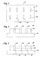
- a light source 50 comprises several different electro-luminescent devices 100, 102, 104, and 106 mounted on an optical panel 75.
- the electro-luminescent devices may differ from each other in geometry, processing, spatial assembly, and function.
- a cross-sectional view of one such electro-luminescent device 100 is schematically shown in Figure 2 .
- Electro-luminescent device 100 includes electrode 110 and an electro-luminescent layer 120 disposed thereon.
- the electro-luminescent layer 120 has a first pattern 130 disposed on a surface adjacent to electrode 110.
- Electro-luminescent layer 120 is made from an electro-luminescent polymeric material and has a substantially uniform thickness.
- the electro-luminescent device 100 further comprises a conductive layer 140 disposed between the electrode 110 and the electro-luminescent layer 120.
- the conductive layer 140 has a second pattern 150 disposed on a surface adjacent to electro-luminescent layer 120.
- the first pattern 130 is identical to the second pattern 150.
- Conductive layer 140 comprises at least one of poly (3,4-ethylenedioxythiophene) (also referred to hereinafter as “PEDOT”), poly (3,4-propylenedioxythiophene) (also referred to hereinafter as “PProDOT”), polystyrenesulfonate (PSS), polyvinylcarbazole (also referred to hereinafter as “PVK”), combinations thereof, and the like.
- Electrode 110 comprises at least one of a metal, indium tin oxide, silicon, and combinations thereof.
- electro-luminescent layer 120 is disposed on one of conductive layer 140 and comprises a first pattern 130.
- First pattern 130 comprises at least one coated portion 160 having a coated surface area and at least one uncoated portion 170 having an uncoated surface area, wherein the at least one uncoated portion 170 intersects the coated portion 160 to form a first coated area 162 and a second coated area 164.
- Coated surface area 160 is frequently greater than the uncoated surface area 170.
- the uncoated portion 170 comprises at least one channel 180 that cuts through coated portion 160 such that the channel 180 has a plurality of walls 190. Each of the plurality of walls 190 has a boundary width 220 of less than 20% of the width of channel 180.
- Coated portion 160 has a thickness in a range from about 50 nm to about 150 nm.
- the electro-luminescent layer 120 comprises a polymeric material such as, but not limited to, conjugated polymers, such as polyfluorenes, polyphenylenes (PPPs), and poly para-(phenylenevinylenes) (PPVs).
- the conductive layer 140 comprises at least one of poly (3,4-ethylenedioxythiophene) (commonly known as "PEDOT”), poly (3,4-propylenedioxythiophene) (also referred to herein as "PProDOT”), polystyrenesulfonate (also referred to herein as "PSS”), polyvinylcarbazole (also referred to herein as "PVK”), and combinations thereof.
- PEDOT poly (3,4-ethylenedioxythiophene)
- PProDOT poly (3,4-propylenedioxythiophene)
- PSS polystyrenesulfonate
- PVK polyvinylcarbazole
- electro-luminescent device 100 further comprises at least one additional polymer layer that performs conductive, emissive, charge injection, and charge blocking functions in the electro-luminescent device 100.
- Electrode 110 comprises a high work function material capable of forming ohmic contact with the upper adjacent layer (conductive layer 140). Electrode 110 comprises at least one of: indium tin oxide; tin oxide; zinc oxide; fluorinated zinc oxide; tin doped zinc oxide; cadmium tin oxide; gold; a conductive polymer comprising at least one of PEDOT, PProDOT, PSS, PVK; and combinations thereof.
- electrode 110 is supported by a substrate material such as, but not limited to, a polycarbonate, a polyolefin, a polyester, a polyimide, a polysulfone, an acrylate, glass, metal foil, and combinations thereof.
- a substrate material such as, but not limited to, a polycarbonate, a polyolefin, a polyester, a polyimide, a polysulfone, an acrylate, glass, metal foil, and combinations thereof.
- an electro-luminescent layer 120 is disclosed for an electro-luminescent device 100.
- the electro-luminescent layer 120 comprises an electro-luminescent polymeric material.
- the electro-luminescent layer 120 is patterned and has a substantially uniform thickness 200, and is formed by forming a continuous layer 115 of the electro-luminescent polymeric material and removing a portion of the continuous layer 115 by wiping a surface 118 of the continuous layer 115 in a direction that is tangential 210 to the surface, as shown in Figure 5 .
- Electro-luminescent layer 120 is disposed adjacent to at least one conductive layer 140. Electro-luminescent layer 120 possesses a pattern 130 comprising at least one coated portion 160 having a coated surface area and at least one uncoated portion 170 having an uncoated surface area, wherein the at least one uncoated portion intersects the coated portion to form a first coated area 162 and a second coated area 164. Typically, the coated surface area is greater than the uncoated surface area. Additionally, the uncoated portion 170 comprises at least one channel 180 that cuts through coated portion 160 such that channel 180 has a plurality of walls 190 each of the plurality of walls 190 has a boundary width 220 of less than 20% of the width of channel 180. Coated surface area 160 has a thickness in a range from about 50 nm to about 150 nm.
- electro-luminescent layer 120 is made from a continuous polymer sheet 115.
- the continuous polymer sheet 115 is formed by depositing a polymeric film, such as PEDOT or the like, on a continuous sheet of a substrate, patterning the polymeric film, and baking the polymeric film at a temperature between about 50°C and about 200°C. The actual baking temperature depends upon the polymer substrate that is used to support the continuous polymer sheet 115.
- the polymeric film is then coated with an electro-luminescent material to form electro-luminescent layer 120 on the polymer film, and the electro-luminescent layer 120 is then patterned.
- the steps of patterning the polymeric film, patterning electro-luminescent layer 120, and baking may be performed in any sequential order.
- Step 1 Step 2 Step 3 Step 4 Step 5 Step 6 Step 7 1.
- Apply PEDOT pattern PEDOT dry bake apply EL pattern EL dry 2.
- Apply PEDOT pattern PEDOT dry bake apply EL dry pattern EL 3.
- Apply PEDOT dry pattern PEDOT bake apply EL pattern EL dry 4.
- Apply PEDOT dry pattern PEDOT bake apply EL dry pattern EL 5.
- Apply PEDOT dry bake pattern PEDOT apply EL pattern EL dry 6.
- PEDOT dry bake pattern PEDOT apply EL dry pattern EL 7. Apply PEDOT dry bake apply EL pattern EL dry pattern PEDOT 8. apply PEDOT dry bake apply EL dry pattern EL pattern PEDOT 9. apply PEDOT dry bake apply EL dry pattern EL and PEDOT simultaneously 10. Apply PEDOT dry apply EL pattern EL dry pattern PEDOT bake 11. apply PEDOT dry apply EL dry pattern EL pattern PEDOT bake 12. apply PEDOT dry apply EL dry pattern EL and PEDOT simultaneously bake 13. apply PEDOT dry apply EL pattern EL dry bake pattern PEDOT 14. apply PEDOT dry apply EL dry bake pattern EL pattern PEDOT 15. apply PEDOT dry apply EL dry bake pattern EL and PEDOT simultaneously
- a portion of the continuous polymer sheet 115 is solvated by at least one of water, methanol, ethanol, isopropanol, acetone, toluene, xylene, and combinations thereof.
- the surface of the solvated portion of continuous polymer sheet 115 is wiped by wiping head 230 remove a portion of at least one film, thereby patterning the film, or films.
- Wiping head 230 comprises at least one of a sponge, elastomer, thermoplastic, thermoset, fiber mat, porous material, polyurethane rubber, synthetic rubber, natural rubber, silicones, polydimethylsiloxane (PDMS), textured materials, and combinations thereof.
- the solvating species are selected for removing a single layer of film with each wiping action without damaging underlying layers.
- the solvating species are selected to facilitate removal of multiple layers with each wiping.
- an electro-luminescent film in a two-layer structure can be patterned using xylene as a solvent without damaging a PEDOT layer underneath.
- two polymer layers can also be removed in one step with a solvent system containing water and xylene.
- isopropanol is used to facilitate mixing of water and xylene to yield a homogeneous solution.
- a method of selectively removing at least one coating from a surface of a substrate comprises the steps of: providing substrate 410 having at least one coating 420 disposed on a surface of the substrate 410; tangentially contacting a portion 460 of coating 420 with wiping head 230; and wiping the portion 460 with wiping head 230 in a direction 210 that is tangential to the surface to remove a portion of coating 420 from substrate 410.
- Coating 420 may be either a wet coating or a dry coating. Alternatively, coating 420 may include both wet and dry regions. In one embodiment, coating 420 is baked onto the surface of substrate 410.
- Wiping head 230 is at least one of a dry wiping head and a wiping head moistened with solvent 250.
- Solvent 250 comprises at least one of a polar solvent, a nonpolar solvent, and combinations thereof.
- Non-limiting examples of solvent 250 include water, methanol, ethanol, isopropanol, acetone, toluene, xylene, and combinations thereof.
- the choice of solvent 250 depends entirely on the coating to be removed.
- wiping head 230 is moistened by injecting solvent 250 into the head 230 while wiping head 230 wipes portion 460 of coating 120.
- wiping head 230 is moistened prior to wiping by at least one of dipping wiping head 230 into a bath containing solvent 250, soaking wiping head 230 in a bath containing solvent 250, spraying either wiping head 230 or portion 460 with solvent 250, or the like.
- Solvent 250 may be either polar or non-polar. For each polymer coating material, there are usually three solubility parameters that account for the non-polar, polar, and hydrogen bonding strength of the polymer. Similarly, there are three corresponding solubility parameters for each solvent. The best solvent for a polymer is one having solubility parameters that match those of the polymer.
- the electro-luminescent layer comprises both (i) a conductive polymer coating, such as PEDOT, which is very polar and dissolves only in hydrogen-bonding solvents like water, and (ii) a light emitting polymer coating that is non-polar, which dissolves only in non-polar solvents such as toluene or xylene.
- a conductive polymer coating such as PEDOT
- a light emitting polymer coating that is non-polar, which dissolves only in non-polar solvents such as toluene or xylene.
- suitable solvents for each polymer are dispersed in a third solvent to produce a homogeneous solution.
- the third, or dispersing, solvent is selected from a number of solvents, such as, but not limited to, alcohols (such as isopropanol, ethanol, methanol, and the like), ketones (such as acetone, methyl ethyl ketone, and the like), acetates, ethers, methylene chloride, or any solvent having intermediate solubility parameters.
- Solvent Light-emitting plastic PEDOT Water 1 5 Methanol 2 2 Ethanol 3 1 Isopropanol 3 1 Acetone 1 1 Toluene 5 1 Xylene 5 1
- Good solvents include either one-component systems having solubility parameters that closely match the solubility parameters of the polymer film (or films), or multi-component solvent systems having effective solubility parameters that match the solubility parameters of the polymer.
- the solvents in the multi-component system do not necessarily have to be a good solvent for the polymer.
- neither CCl 4 nor ethanol are good individual solvents for polymethylmethacrylate (PMMA), but a binary mixture of CCl 4 and ethanol is a good solvent for PMMA because the effective solubility parameter of the mixture matches that of PMMA.
- Example 3 Wiping Example - Selective removal of top coating without damaging underlying layer.
- a PEDOT layer is spin coated onto an indium tin oxide (ITO) coated glass substrate and baked at 200°C for 1 hour.
- a layer of light emitting plastic i.e., electro-luminescent layer
- the patterned area is wiped by solvent assisted wiping (SAW) in which xylene was the only solvent used to remove portions of the electro-luminescent layer.
- Example 4 Wiping Example - Simultaneous removal of both coating layers
- the PEDOT layer is spin coated onto an indium tin oxide (ITO) coated glass substrate and baked at 200°C for 1 hour.
- a layer of light emitting plastic (or electro-luminescent layer) is spin-coated on top of the PEDOT layer.
- the patterned area is wiped by solvent assisted wiping (SAW) with a solvent mixture consisting of water, isopropanol, and xylene so as to remove both PEDOT and electro-luminescent layers.
- SAW solvent assisted wiping
- Wiping head 230 comprises at least one of a sponge, an elastomer, a thermoplastic, a thermoset, a fiber mat, a porous material, polyurethane rubber, synthetic rubber, natural rubber, silicones, PDMS, textured materials, and combinations thereof.
- wiping head 230 is a fixed head.
- wiping head 230 is movable with respect to substrate 110.
- wiping head 230 and substrate 110 may be moved simultaneously with respect to each other.
- wiping head 230 is rotatable.
- wiping head 230 is a rotatable wheel.
- the step of tangentially contacting a portion 460 ( Figure 7B ) of the at least one coating 420 with wiping head 230 comprises contacting a portion 460 of the at least one coating 420 in a tangential direction 210 with a contact surface of wiping head 230.
- a schematic cross-sectional view of the contact surface of wiping head 230 is shown in Figure 6 .
- the contact surface 240 has a predetermined structure, or geometry.
- the predetermined structure comprises at least one prism 280, with the at least one prism 280 having a predetermined angle 290.
- the at least one prism 280 has a geometric profile, such as a pointed profile or tip, a square profile, a trapezoidal profile, a rounded profile or tip, and the like.
- the predetermined geometry comprises a plurality of prisms 280, wherein the plurality of prisms 280 are separated from each other by a predetermined pitch 300, as shown in Figure 6 .
- the plurality of prism may include prisms having the same profile, or prisms having different profiles, arranged in either a random or predetermined regular order.
- pitch 300 is about 50 microns.
- Wiping head 230 has a structure comprising a plurality of protrusions, such as, for example, plurality of prisms 280, to apply concentrated force to portion 460 so as to remove portion 460 and pattern the film. Wiping head protrusions are separated by indentations for carrying solvent to the film surface.
- the film surface is either moistened or premoistened by solvent in the liquid phase. In another embodiment, the film surface is moistened or premoistened by solvent in the vapor phase.
- the contact surface further includes at least one sidewall 260 disposed on at least one edge of the contact surface 240.
- the method further includes the step of premoistening portion 460 ( Figure 7A ) prior to wiping portion 460 with wiping head 230.
- the step of wiping the portion 460 with the wiping head to remove the portion 460 of the at least one coating 420 from the substrate 410 comprises translating the substrate 410 in a predetermined direction with respect to wiping head 230.
- wiping head 230 wipes the portion 460 in a direction parallel to the predetermined direction.
- wiping head 230 wipes the portion 460 in a direction other than parallel to the predetermined direction.
- the step of providing the substrate 410 comprises providing a continuous sheet of the substrate from a supply roll.
- the method further includes the step of collecting the continuous sheet on a take-up roll.
- an apparatus for selectively removing a portion 460 at least one coating 420 from a surface of a substrate 410.
- the apparatus comprises a means for supplying the substrate 410 having the at least one coating 420, a wiping head 230 for removing a portion 460 of the at least one coating 420, wherein the wiping head 230 contacts the at least one coating 420 in a tangential direction 210, and a means for collecting the substrate after removing the portion 460.
- a wiping head 230 for removing a portion 460 of at least one coating 420 disposed on a surface of a substrate 410.
- the wiping head 230 comprises a contact surface 240 for contacting and removing portion 460, wherein contact surface 240 contacts portion 460 in a tangential direction 210, and wherein contact surface 240 has a predetermined structure.
Landscapes
- Engineering & Computer Science (AREA)
- Manufacturing & Machinery (AREA)
- Electroluminescent Light Sources (AREA)
- Application Of Or Painting With Fluid Materials (AREA)
- Manufacturing Of Printed Circuit Boards (AREA)
Abstract
Description
- This invention relates to a method of uniformly patterning an electro-luminescent layer of electro-luminescent devices.
- Electro-active devices, such as organic light emitting diodes (referred hereinafter to as "OLEDs"), are widely used in organic transistors, fuel cell components, microelectronics processing, microanalytical test procedures, and in specialty electronics. One of the features of such devices is an electro-luminescent layer, formed from photo-sensitive materials, that emits light on receiving an electrical impulse. In order to facilitate miniaturization, conform to device geometry, and maximize electro-luminescent yield, the electro-luminescent layer must often be patterned to various textures, topography, and geometries.
- Electro-luminescent layer patterning has been conventionally performed using stamping or laser ablation. In stamping, a pattern is imprinted upon the layer using mechanical force upon a patterned die or a stamping head, whereas in laser ablation, a patterned photomask covers the area to be patterned while the remaining area is selectively etched using a laser beam.
- One problem associated with such patterning of electro-luminescent layers is that stamping leaves behind a substantial amount of material residue on the layer surface. Patterning by stamping also does not guarantee uniform, reproducible, and precise patterning over large specimens. While laser ablation may yield uniform, reproducible, and precisely patterned surfaces, the process needs high vacuum conditions, produces excessive debris around the patterned area, is expensive, and cannot be performed on large specimens or in fieldwork.
-
EP-1351303 discloses an organic light emitting display device for displaying selected images from a plurality of images, each with one or more desired colors and also describes a method of fabrication. -
US-2002/0158295 describes an electrochemical transit device comprising a source contact, a drain contact and at least one gate electrode. The deposited layers may be structured by subtractive techniques such as scratching, scaring or scraping. Also described are displays incorporating such devices and processes for the production of such devices. - The current methods for patterning an electro-luminescent layer in electro-active devices use mechanical or laser-beam techniques that do not enable patterned surfaces to be patterned to precision in minimal turnaround times. Therefore, what is needed is an electro-active device having an electro-luminescent layer that is precisely and quickly patterned to uniform thickness. What is also needed is a method for patterning such an electro-luminescent layer that is applicable to a variety of material compositions with a variety of solvating species. What is also needed is a patterning method that is effectively independent of the processing or forming history of the electro-luminescent film.
- The present invention meets these and other needs by providing a patterned electro-luminescent layer of substantially uniform thickness and a method and apparatus for forming patterned electro-luminescent layer of substantially uniform thickness on a continuous electroluminescent film. Different kinds of electro-luminescent layers can be patterned by this method. The invention also includes an apparatus for making an electro-luminescent layer by selectively removing at least one coating from a surface of a substrate.
- According to a first aspect of the invention, there is provided a method of selectively removing at least one coating from a surface of a continuous electroluminescent film, the method comprising the steps of a) providing the electroluminescent film, the electroluminescent film having the at least one coating disposed on the surface; and b) contacting a portion of the at least one coating with a coating removing means; wherein c) said coating removing means comprises a wiping head which has solvents for solvating the electroluminescent film; and wherein said method of selectively removing at least one coating comprises d) wiping the portion with the wiping head in a direction that is tangential to the surface to remove the portion of the at least one coating from the substrate.
- The least one coating may be a wet or dry coating.
- The at least one coating may have been baked onto the surface of electroluminescent film.
- The solvents may include at least one of water, methanol, ethanol, isopropanol, acetone, toluene xylene and combinations thereof.
- According to a second aspect of the invention, there is provided an apparatus for selectively removing at least one coating from a surface of a continuous electroluminescent film, the apparatus comprising a) a means for supplying the electroluminescent film having the at least one coating; and b) a means for removing for removing a portion of the at least one coating; wherein said removing means comprises c) a wiping head, which has solvents for solvating the electroluminescent film, for removing a portion of the at least one coating, wherein the wiping head tangentially contacts the at least one coating; and wherein said apparatus comprises d) a means for collecting the electroluminescent film after removing the portion.
- The solvents may include at least one of water, methanol, ethanol, isopropanol, acetone, toluene xylene and combinations thereof.
- The wiping head may be moistened by injecting the solvents into the wiping head while the wiping head wipes the portion of the at least one coating.
- The wiping head may comprise at least one of a sponge, an elastomer, a thermoplastic, a thermoset, a fiber mat, a porous material, polyurethane rubber, synthetic rubber, natural rubber, silicones, polydimethylsiloxane , textured materials and combinations thereof.
- These and other aspects, advantages, and salient features of the present invention will become apparent from the following detailed description, the accompanying drawings, and the appended claims.
-
-
FIGURE 1 is a schematic view of a light source comprising a plurality of electro-luminescent devices on an optical panel; -
FIGURE 2 is a cross-sectional view of an electro-luminescent device; -
FIGURE 3 is a schematic view of one embodiment of an electro-luminescent device with its constituent patterns; -
FIGURE 4 is a schematic view of a second embodiment of a patterned electro-luminescent device having a coated portion and uncoated portion; -
FIGURE 5 is a schematic view of an embodiment for removing a portion of continuous sheet by wiping;FIGURE 6 is a schematic cross-sectional view of the contact surface of a wiping head of the present invention; -
FIGURE 7A is a schematic view of a method of selectively removing at least one coating from a surface of a substrate; and -
FIGURE 7B is a second schematic view of a method of selectively removing at least one coating from a surface of a substrate. - In the following description, like reference characters designate like or corresponding parts throughout the several views shown in the figures. It is also understood that terms such as "top", "bottom", "outward", "inward", and the like are words of convenience and are not to be construed as limiting terms.
- Referring to the drawings in general and to
Figure 1 in particular, it will be understood that the illustrations are for the purpose of describing a preferred embodiment of the invention and are not intended to limit the invention thereto. - Visible light sources produce light in different ways. Such devices may comprise different components and mechanisms for producing light and some sources may produce light more efficiently than others. Many light sources are made of electro-luminescent materials arranged as coatings or films upon an electro-active substrate (often called an electrode). Consequently, the film may be patterned or textured to suit design requirements.
- Common methods of film patterning, such as ink jet printing, deposit the coating one drop at a time, by creating polyimide wells to position the drop on the film surface. This method is commonly used in pixels for displays. Films may also be patterned or textured using methods such as, but not limited to, screen printing, gravure printing, flexographic printing, offset lithographic printing, spin coating, spray coating, meniscus coating, and dip coating. However, it is difficult to dispose and pattern coating layers of uniform thickness using such methods with subsequent solvent deposition in which the solvent creates a crater or channel upon drying. One embodiment of the present invention discloses a patterning method applicable to large area devices with coatings of uniform thickness. A common approach to producing patterned electro-luminescent film is to selectively remove portions of the electro-luminescent coating from a continuous film of the electro-luminescent material. This is conventionally done using laser ablation, plasma etching, scratching the film surface, tape lifting and lifting off under high temperature or pressure using a die or stamp. However, there are certain disadvantages associated with each of these methods. For instance, laser ablation and plasma etching focus on small working areas of the specimen, and the cost for scaling up the process can be very high. Scratching requires plowing through the continuous coating with a stiff stylus, which can potentially damage the underlying layers or substrates. Stamping and lifting with a rubbery die offer an affordable but qualitatively unacceptable solution. The liftoff process can be uniquely related to the materials of construction of the die and may result in incomplete coating removal with residues deposited on the stamped area. The residues can also affect the final properties and performance of the electro-luminescent device.
- The present invention provides a process to selectively remove a portion of a continuous electro-luminescent film and to produce a sharply patterned electro-luminescent film.
- The invention provides a process to remove coating material from a continuous electro-luminescent film via wiping with a 'moistened' soft head. The wiping head contains solvents that solvate (or moisten, using aqueous or non-aqueous solvents) the electro-luminescent film. A tangential wiping action using the wiping head assists in removing the solvated area.
- In another embodiment, the invention also provides a solvent system that enables removal of portions of multiple layers of film in a single step. The multiple layers may either be identical or distinct from each other.
- In one embodiment of the present invention, shown in
Figure 1 , alight source 50 comprises several different electro-luminescent devices optical panel 75. The electro-luminescent devices may differ from each other in geometry, processing, spatial assembly, and function. A cross-sectional view of one such electro-luminescent device 100 is schematically shown inFigure 2 . Electro-luminescent device 100 includeselectrode 110 and an electro-luminescent layer 120 disposed thereon. The electro-luminescent layer 120 has afirst pattern 130 disposed on a surface adjacent toelectrode 110. Electro-luminescent layer 120 is made from an electro-luminescent polymeric material and has a substantially uniform thickness. In another embodiment, shown inFigure 3 , the electro-luminescent device 100 further comprises aconductive layer 140 disposed between theelectrode 110 and the electro-luminescent layer 120. Theconductive layer 140 has asecond pattern 150 disposed on a surface adjacent to electro-luminescent layer 120. In yet another embodiment, thefirst pattern 130 is identical to thesecond pattern 150.Conductive layer 140 comprises at least one of poly (3,4-ethylenedioxythiophene) (also referred to hereinafter as "PEDOT"), poly (3,4-propylenedioxythiophene) (also referred to hereinafter as "PProDOT"), polystyrenesulfonate (PSS), polyvinylcarbazole (also referred to hereinafter as "PVK"), combinations thereof, and the like.Electrode 110 comprises at least one of a metal, indium tin oxide, silicon, and combinations thereof. - In the embodiment shown in
Figure 4 , electro-luminescent layer 120 is disposed on one ofconductive layer 140 and comprises afirst pattern 130.First pattern 130 comprises at least onecoated portion 160 having a coated surface area and at least oneuncoated portion 170 having an uncoated surface area, wherein the at least oneuncoated portion 170 intersects thecoated portion 160 to form a firstcoated area 162 and a secondcoated area 164. Coatedsurface area 160 is frequently greater than theuncoated surface area 170. Additionally, theuncoated portion 170 comprises at least onechannel 180 that cuts through coatedportion 160 such that thechannel 180 has a plurality ofwalls 190. Each of the plurality ofwalls 190 has aboundary width 220 of less than 20% of the width ofchannel 180.Coated portion 160 has a thickness in a range from about 50 nm to about 150 nm. - The electro-
luminescent layer 120 comprises a polymeric material such as, but not limited to, conjugated polymers, such as polyfluorenes, polyphenylenes (PPPs), and poly para-(phenylenevinylenes) (PPVs). Theconductive layer 140 comprises at least one of poly (3,4-ethylenedioxythiophene) (commonly known as "PEDOT"), poly (3,4-propylenedioxythiophene) (also referred to herein as "PProDOT"), polystyrenesulfonate (also referred to herein as "PSS"), polyvinylcarbazole (also referred to herein as "PVK"), and combinations thereof. In other embodiments of the invention, electro-luminescent device 100 further comprises at least one additional polymer layer that performs conductive, emissive, charge injection, and charge blocking functions in the electro-luminescent device 100.Electrode 110 comprises a high work function material capable of forming ohmic contact with the upper adjacent layer (conductive layer 140).Electrode 110 comprises at least one of: indium tin oxide; tin oxide; zinc oxide; fluorinated zinc oxide; tin doped zinc oxide; cadmium tin oxide; gold; a conductive polymer comprising at least one of PEDOT, PProDOT, PSS, PVK; and combinations thereof. In other embodiments of the invention,electrode 110 is supported by a substrate material such as, but not limited to, a polycarbonate, a polyolefin, a polyester, a polyimide, a polysulfone, an acrylate, glass, metal foil, and combinations thereof. - In another embodiment of the present invention, an electro-
luminescent layer 120 is disclosed for an electro-luminescent device 100. The electro-luminescent layer 120 comprises an electro-luminescent polymeric material. The electro-luminescent layer 120 is patterned and has a substantiallyuniform thickness 200, and is formed by forming acontinuous layer 115 of the electro-luminescent polymeric material and removing a portion of thecontinuous layer 115 by wiping asurface 118 of thecontinuous layer 115 in a direction that is tangential 210 to the surface, as shown inFigure 5 . - Electro-
luminescent layer 120 is disposed adjacent to at least oneconductive layer 140. Electro-luminescent layer 120 possesses apattern 130 comprising at least onecoated portion 160 having a coated surface area and at least oneuncoated portion 170 having an uncoated surface area, wherein the at least one uncoated portion intersects the coated portion to form a firstcoated area 162 and a secondcoated area 164. Typically, the coated surface area is greater than the uncoated surface area. Additionally, theuncoated portion 170 comprises at least onechannel 180 that cuts through coatedportion 160 such thatchannel 180 has a plurality ofwalls 190 each of the plurality ofwalls 190 has aboundary width 220 of less than 20% of the width ofchannel 180. Coatedsurface area 160 has a thickness in a range from about 50 nm to about 150 nm. - In one embodiment, electro-
luminescent layer 120 is made from acontinuous polymer sheet 115. Thecontinuous polymer sheet 115 is formed by depositing a polymeric film, such as PEDOT or the like, on a continuous sheet of a substrate, patterning the polymeric film, and baking the polymeric film at a temperature between about 50°C and about 200°C. The actual baking temperature depends upon the polymer substrate that is used to support thecontinuous polymer sheet 115. The polymeric film is then coated with an electro-luminescent material to form electro-luminescent layer 120 on the polymer film, and the electro-luminescent layer 120 is then patterned. The steps of patterning the polymeric film, patterning electro-luminescent layer 120, and baking may be performed in any sequential order. For example, application of polymeric and electro-luminescent films, patterning, and baking may proceed according to any of the sequences shown in Table 1.Table 1: Different, non-limiting embodiments of the present invention showing various process methods in PEDOT film application and patterning. In the table, "EL" refers to the application of electro-luminescent film. S1. Step 1 Step 2 Step 3 Step 4 Step 5 Step 6 Step 7 1. apply PEDOT pattern PEDOT dry bake apply EL pattern EL dry 2. apply PEDOT pattern PEDOT dry bake apply EL dry pattern EL 3. apply PEDOT dry pattern PEDOT bake apply EL pattern EL dry 4. apply PEDOT dry pattern PEDOT bake apply EL dry pattern EL 5. apply PEDOT dry bake pattern PEDOT apply EL pattern EL dry 6. apply PEDOT dry bake pattern PEDOT apply EL dry pattern EL 7. apply PEDOT dry bake apply EL pattern EL dry pattern PEDOT 8. apply PEDOT dry bake apply EL dry pattern EL pattern PEDOT 9. apply PEDOT dry bake apply EL dry pattern EL and PEDOT simultaneously 10. apply PEDOT dry apply EL pattern EL dry pattern PEDOT bake 11. apply PEDOT dry apply EL dry pattern EL pattern PEDOT bake 12. apply PEDOT dry apply EL dry pattern EL and PEDOT simultaneously bake 13. apply PEDOT dry apply EL pattern EL dry bake pattern PEDOT 14. apply PEDOT dry apply EL dry bake pattern EL pattern PEDOT 15. apply PEDOT dry apply EL dry bake pattern EL and PEDOT simultaneously - To facilitate film removal over a selected area of the electro-luminescent film, a portion of the
continuous polymer sheet 115 is solvated by at least one of water, methanol, ethanol, isopropanol, acetone, toluene, xylene, and combinations thereof. The surface of the solvated portion ofcontinuous polymer sheet 115 is wiped by wipinghead 230 remove a portion of at least one film, thereby patterning the film, or films. Wipinghead 230 comprises at least one of a sponge, elastomer, thermoplastic, thermoset, fiber mat, porous material, polyurethane rubber, synthetic rubber, natural rubber, silicones, polydimethylsiloxane (PDMS), textured materials, and combinations thereof. - In one embodiment of the invention, the solvating species are selected for removing a single layer of film with each wiping action without damaging underlying layers. In another embodiment, the solvating species are selected to facilitate removal of multiple layers with each wiping. For example, an electro-luminescent film in a two-layer structure can be patterned using xylene as a solvent without damaging a PEDOT layer underneath. In yet another embodiment, two polymer layers can also be removed in one step with a solvent system containing water and xylene. In this particular embodiment, isopropanol is used to facilitate mixing of water and xylene to yield a homogeneous solution.
- In another embodiment of the claimed invention, a method of selectively removing at least one coating from a surface of a substrate is disclosed and generally shown in
Figures 7A and 7B . The method comprises the steps of: providingsubstrate 410 having at least onecoating 420 disposed on a surface of thesubstrate 410; tangentially contacting aportion 460 ofcoating 420 with wipinghead 230; and wiping theportion 460 with wipinghead 230 in adirection 210 that is tangential to the surface to remove a portion of coating 420 fromsubstrate 410. Coating 420 may be either a wet coating or a dry coating. Alternatively, coating 420 may include both wet and dry regions. In one embodiment, coating 420 is baked onto the surface ofsubstrate 410. Wipinghead 230 is at least one of a dry wiping head and a wiping head moistened with solvent 250. Solvent 250 comprises at least one of a polar solvent, a nonpolar solvent, and combinations thereof. Non-limiting examples of solvent 250 include water, methanol, ethanol, isopropanol, acetone, toluene, xylene, and combinations thereof. The choice of solvent 250 depends entirely on the coating to be removed. In one embodiment, wipinghead 230 is moistened by injecting solvent 250 into thehead 230 while wipinghead 230 wipesportion 460 ofcoating 120. In another embodiment, wipinghead 230 is moistened prior to wiping by at least one of dippingwiping head 230 into a bath containing solvent 250, soaking wipinghead 230 in a bath containing solvent 250, spraying either wipinghead 230 orportion 460 with solvent 250, or the like. - Solvent 250 may be either polar or non-polar. For each polymer coating material, there are usually three solubility parameters that account for the non-polar, polar, and hydrogen bonding strength of the polymer. Similarly, there are three corresponding solubility parameters for each solvent. The best solvent for a polymer is one having solubility parameters that match those of the polymer.
- In typical instances, the electro-luminescent layer comprises both (i) a conductive polymer coating, such as PEDOT, which is very polar and dissolves only in hydrogen-bonding solvents like water, and (ii) a light emitting polymer coating that is non-polar, which dissolves only in non-polar solvents such as toluene or xylene. In order to remove multiple polymer coatings having extremely divergent solubility characteristics in a single wipe, suitable solvents for each polymer are dispersed in a third solvent to produce a homogeneous solution. The third, or dispersing, solvent is selected from a number of solvents, such as, but not limited to, alcohols (such as isopropanol, ethanol, methanol, and the like), ketones (such as acetone, methyl ethyl ketone, and the like), acetates, ethers, methylene chloride, or any solvent having intermediate solubility parameters. The solvent ratings for a typical light-emitting plastic and PEDOT are listed in Table 1.
Table 1: Solvent rating for polymers (1 = low solubility or insoluble; 5 = high solubility). Solvent Light-emitting plastic PEDOT Water 1 5 Methanol 2 2 Ethanol 3 1 Isopropanol 3 1 Acetone 1 1 Toluene 5 1 Xylene 5 1 - Good solvents include either one-component systems having solubility parameters that closely match the solubility parameters of the polymer film (or films), or multi-component solvent systems having effective solubility parameters that match the solubility parameters of the polymer. The solvents in the multi-component system do not necessarily have to be a good solvent for the polymer. For example, neither CCl4 nor ethanol are good individual solvents for polymethylmethacrylate (PMMA), but a binary mixture of CCl4 and ethanol is a good solvent for PMMA because the effective solubility parameter of the mixture matches that of PMMA.
- In this example, a PEDOT layer is spin coated onto an indium tin oxide (ITO) coated glass substrate and baked at 200°C for 1 hour. A layer of light emitting plastic (i.e., electro-luminescent layer) is then spin-coated on top of the PEDOT layer. The patterned area is wiped by solvent assisted wiping (SAW) in which xylene was the only solvent used to remove portions of the electro-luminescent layer.
- The PEDOT layer is spin coated onto an indium tin oxide (ITO) coated glass substrate and baked at 200°C for 1 hour. A layer of light emitting plastic (or electro-luminescent layer) is spin-coated on top of the PEDOT layer. The patterned area is wiped by solvent assisted wiping (SAW) with a solvent mixture consisting of water, isopropanol, and xylene so as to remove both PEDOT and electro-luminescent layers.
- Wiping
head 230 comprises at least one of a sponge, an elastomer, a thermoplastic, a thermoset, a fiber mat, a porous material, polyurethane rubber, synthetic rubber, natural rubber, silicones, PDMS, textured materials, and combinations thereof. In one embodiment of the invention, wipinghead 230 is a fixed head. In another embodiment, wipinghead 230 is movable with respect tosubstrate 110. Alternatively, wipinghead 230 andsubstrate 110 may be moved simultaneously with respect to each other. In still another embodiment, wipinghead 230 is rotatable. In a further embodiment, wipinghead 230 is a rotatable wheel. - The step of tangentially contacting a portion 460 (
Figure 7B ) of the at least onecoating 420 with wipinghead 230 comprises contacting aportion 460 of the at least onecoating 420 in atangential direction 210 with a contact surface of wipinghead 230. A schematic cross-sectional view of the contact surface of wipinghead 230 is shown inFigure 6 . In one embodiment, shown inFigure 6 , thecontact surface 240 has a predetermined structure, or geometry. In one embodiment, the predetermined structure comprises at least oneprism 280, with the at least oneprism 280 having apredetermined angle 290. The at least oneprism 280 has a geometric profile, such as a pointed profile or tip, a square profile, a trapezoidal profile, a rounded profile or tip, and the like. In another embodiment, the predetermined geometry comprises a plurality ofprisms 280, wherein the plurality ofprisms 280 are separated from each other by apredetermined pitch 300, as shown inFigure 6 . The plurality of prism may include prisms having the same profile, or prisms having different profiles, arranged in either a random or predetermined regular order. In one embodiment,pitch 300 is about 50 microns. Wipinghead 230 has a structure comprising a plurality of protrusions, such as, for example, plurality ofprisms 280, to apply concentrated force toportion 460 so as to removeportion 460 and pattern the film. Wiping head protrusions are separated by indentations for carrying solvent to the film surface. The film surface is either moistened or premoistened by solvent in the liquid phase. In another embodiment, the film surface is moistened or premoistened by solvent in the vapor phase. - In one embodiment of the claimed method, the contact surface further includes at least one
sidewall 260 disposed on at least one edge of thecontact surface 240. In another embodiment, the method further includes the step of premoistening portion 460 (Figure 7A ) prior to wipingportion 460 with wipinghead 230. The step of wiping theportion 460 with the wiping head to remove theportion 460 of the at least onecoating 420 from the substrate 410 (Figure 7A ) comprises translating thesubstrate 410 in a predetermined direction with respect to wipinghead 230. In another embodiment, wipinghead 230 wipes theportion 460 in a direction parallel to the predetermined direction. In another embodiment, wipinghead 230 wipes theportion 460 in a direction other than parallel to the predetermined direction. In another embodiment, the step of providing thesubstrate 410 comprises providing a continuous sheet of the substrate from a supply roll. In another embodiment the method further includes the step of collecting the continuous sheet on a take-up roll. - In another embodiment of the claimed invention, an apparatus is disclosed for selectively removing a
portion 460 at least onecoating 420 from a surface of asubstrate 410. The apparatus comprises a means for supplying thesubstrate 410 having the at least onecoating 420, a wipinghead 230 for removing aportion 460 of the at least onecoating 420, wherein the wipinghead 230 contacts the at least onecoating 420 in atangential direction 210, and a means for collecting the substrate after removing theportion 460. - In another embodiment of the claimed invention, a wiping
head 230 is disclosed for removing aportion 460 of at least onecoating 420 disposed on a surface of asubstrate 410. The wipinghead 230 comprises acontact surface 240 for contacting and removingportion 460, whereincontact surface 240contacts portion 460 in atangential direction 210, and whereincontact surface 240 has a predetermined structure. - Although the examples described hereinabove are for an electroluminescent device, it is understood that the invention can be used in manufacturing features of other articles and devices, such as, but not limited to, microelectronic devices, photovoltaics, thin film transistors, electronic paper and displays, photonic devices, waveguides; microelectromechanical systems (MEMS), microfluidics devices, and the like.
Claims (9)
- A method of selectively removing at least one coating (420) from a surface of a continuous electroluminescent film (410), the method comprising the steps of:a) providing the electroluminescent film (410), the electroluminescent film (410) having the at least one coating (420) disposed on the surface;b) contacting a portion (460) of the at least one coating (420) with a coating removing means (230); and
characterized in thatc) said coating removing means comprises a wiping head (230) which has solvents for solvating the electroluminescent film;
and further in that said method of selectively removing at least one coating (420) comprises:d) wiping the portion with the wiping head (230) in a direction that is tangential (210) to the surface to remove the portion (460) of the at least one coating (420) from the electroluminescent film(410). - The method of claim 1, wherein the at least one coating is a wet coating.
- The method of claim 1, wherein the at least one coating is a dry coating.
- The method of claim 1, wherein the at least one coating is has been baked onto the surface of electroluminescent film.
- The method of any preceding claim wherein the solvents include at least one of water, methanol, ethanol, isopropanol, acetone, toluene xylene and combinations thereof.
- An apparatus for selectively removing at least one coating (420) from a surface of a continuous electroluminescent film (410), the apparatus comprising:a) a means for supplying the electroluminescent film (410) having the at least one coating (420);b) a means for removing for removing a portion (460) of the at least one coating (420);
characterized in that said removing means comprisesc) a wiping head (230), which has solvents for solvating the electroluminescent film, for removing a portion (460) of the at least one coating (420), wherein the wiping head tangentially (210) contacts the at least one coating (420);
and further in that said apparatus comprisesd) a means for collecting the electroluminescent film (410) after removing the portion. - The apparatus of claim 6, wherein the solvents include at least one of water, methanol, ethanol, isopropanol, acetone, toluene xylene and combinations thereof.
- The apparatus of claim 6 or 7, wherein the wiping head is moistened by injecting the solvents into the wiping head while the wiping head wipes the portion of the at least one coating.
- The apparatus of claim 6, 7 or 8, wherein the wiping head comprises at least one of a sponge, an elastomer, a thermoplastic, a thermoset, a fiber mat, a porous material, polyurethane rubber, synthetic rubber, natural rubber, silicones, polydimethylsiloxane , textured materials and combinations thereof.
Applications Claiming Priority (2)
| Application Number | Priority Date | Filing Date | Title |
|---|---|---|---|
| US10/735,503 US20050129977A1 (en) | 2003-12-12 | 2003-12-12 | Method and apparatus for forming patterned coated films |
| PCT/US2004/037014 WO2005062399A1 (en) | 2003-12-12 | 2004-11-08 | Method and apparatus for forming patterned coated films |
Publications (2)
| Publication Number | Publication Date |
|---|---|
| EP1695398A1 EP1695398A1 (en) | 2006-08-30 |
| EP1695398B1 true EP1695398B1 (en) | 2009-11-04 |
Family
ID=34653633
Family Applications (1)
| Application Number | Title | Priority Date | Filing Date |
|---|---|---|---|
| EP04810440A Expired - Lifetime EP1695398B1 (en) | 2003-12-12 | 2004-11-08 | Method and apparatus for forming patterned coated films |
Country Status (9)
| Country | Link |
|---|---|
| US (2) | US20050129977A1 (en) |
| EP (1) | EP1695398B1 (en) |
| JP (1) | JP4937757B2 (en) |
| KR (1) | KR101392781B1 (en) |
| CN (1) | CN1902770B (en) |
| AT (1) | ATE447770T1 (en) |
| DE (1) | DE602004023966D1 (en) |
| SG (1) | SG149015A1 (en) |
| WO (1) | WO2005062399A1 (en) |
Families Citing this family (17)
| Publication number | Priority date | Publication date | Assignee | Title |
|---|---|---|---|---|
| DE202005002110U1 (en) * | 2004-02-19 | 2005-05-04 | Hong-Yuan Technology Co., Ltd., Yonghe | Light-emitting device |
| US20070200489A1 (en) * | 2006-02-01 | 2007-08-30 | Poon Hak F | Large area organic electronic devices and methods of fabricating the same |
| WO2007106699A1 (en) * | 2006-03-14 | 2007-09-20 | Cabot Corporation | Roll-to-roll manufacturing of electronic and optical materials |
| DE102007005089B3 (en) * | 2007-02-01 | 2008-09-25 | Leonhard Kurz Gmbh & Co. Kg | Production of polymer based solar cell, comprises allocating a lattice like structured free surface area in the form of openings having first electrode, filling the area with lacquer and forming a second electrode on active layer structure |
| US20090149589A1 (en) * | 2007-12-05 | 2009-06-11 | College Of William And Mary | Method for generating surface-silvered polymer structures |
| US7741140B2 (en) * | 2008-01-21 | 2010-06-22 | General Electric Company | Methods, apparatus, and rollers for cross-web forming of optoelectronic devices |
| US20090186550A1 (en) * | 2008-01-21 | 2009-07-23 | General Electric Company | Methods, apparatus, and rollers for forming optoelectronic devices |
| US20090214828A1 (en) * | 2008-02-26 | 2009-08-27 | Vicki Herzl Watkins | Blunt tip prism film and methods for making the same |
| US8409672B2 (en) * | 2008-04-24 | 2013-04-02 | Semiconductor Energy Laboratory Co., Ltd. | Method of manufacturing evaporation donor substrate and method of manufacturing light-emitting device |
| WO2010004888A1 (en) * | 2008-07-08 | 2010-01-14 | コニカミノルタホールディングス株式会社 | Organic electroluminescent element fabrication method |
| US20110065282A1 (en) | 2009-09-11 | 2011-03-17 | General Electric Company | Apparatus and methods to form a patterned coating on an oled substrate |
| US8137148B2 (en) * | 2009-09-30 | 2012-03-20 | General Electric Company | Method of manufacturing monolithic parallel interconnect structure |
| JP4893839B2 (en) * | 2010-03-29 | 2012-03-07 | 住友化学株式会社 | Method for manufacturing light emitting device |
| GB201011282D0 (en) | 2010-07-05 | 2010-08-18 | Cambridge Entpr Ltd | Patterning |
| GB201011280D0 (en) * | 2010-07-05 | 2010-08-18 | Cambridge Entpr Ltd | Patterning |
| KR101434658B1 (en) * | 2011-12-28 | 2014-08-29 | 코오롱인더스트리 주식회사 | Manufacturing for polymer solar cell |
| KR20150102180A (en) * | 2014-02-27 | 2015-09-07 | 삼성디스플레이 주식회사 | Laser beam irradiation apparatus and manufacturing method of organic light emitting display apparatus using the same |
Family Cites Families (28)
| Publication number | Priority date | Publication date | Assignee | Title |
|---|---|---|---|---|
| US89211A (en) * | 1869-04-20 | Improved machine for making bolt-heads | ||
| US59985A (en) * | 1866-11-27 | Eeuben e | ||
| US36738A (en) * | 1862-10-21 | Improvement in machinery for sizing the backs of carpets | ||
| US63700A (en) * | 1867-04-09 | Improved blacking case | ||
| US1065725A (en) * | 1913-04-02 | 1913-06-24 | Samuel S Riegel | Locomotive-grate shaker. |
| US3837747A (en) * | 1973-01-30 | 1974-09-24 | U Seymore | Washer/squeegee |
| JPH0695508B2 (en) * | 1986-11-28 | 1994-11-24 | 大日本スクリ−ン製造株式会社 | Double-sided cleaning device for substrates |
| DE4329178B4 (en) * | 1993-08-30 | 2006-11-09 | EMO Oberflächentechnik GmbH | Vapor cleaning |
| US6357507B1 (en) * | 1995-03-22 | 2002-03-19 | Räsontec N.V. Rabobank Trust Comp. Curacao N.V. | Curtain arrangement for preventing spread of smoke |
| US6563493B2 (en) * | 1997-06-30 | 2003-05-13 | Canon Kabushiki Kaisha | Molded article of pen tip of input pen for coordinate input apparatus, method of molding pen tip and mold therefor |
| US6260264B1 (en) * | 1997-12-08 | 2001-07-17 | 3M Innovative Properties Company | Methods for making z-axis electrical connections |
| DE19920593B4 (en) * | 1999-05-05 | 2006-07-13 | Assa Abloy Identification Technology Group Ab | Chip carrier for a chip module and method for producing the chip module |
| JP2001196167A (en) * | 2000-01-07 | 2001-07-19 | Dainippon Printing Co Ltd | Electroluminescent substrate, electroluminescent device, and method of manufacturing the same |
| US6699728B2 (en) * | 2000-09-06 | 2004-03-02 | Osram Opto Semiconductors Gmbh | Patterning of electrodes in oled devices |
| GB0024294D0 (en) * | 2000-10-04 | 2000-11-15 | Univ Cambridge Tech | Solid state embossing of polymer devices |
| EP1327264A1 (en) | 2000-10-17 | 2003-07-16 | 3M Innovative Properties Company | Solvent assisted burnishing of pre-underfilled solder-bumped wafers for flipchip bonding |
| US6515314B1 (en) * | 2000-11-16 | 2003-02-04 | General Electric Company | Light-emitting device with organic layer doped with photoluminescent material |
| CN100397678C (en) * | 2000-12-26 | 2008-06-25 | Lg化学株式会社 | Electronic devices containing organic compounds with p-type semiconducting properties |
| US6648398B2 (en) * | 2001-01-09 | 2003-11-18 | M&C Corporation | Bed panel with torsion pin hinge |
| SE520339C2 (en) * | 2001-03-07 | 2003-06-24 | Acreo Ab | Electrochemical transistor device and its manufacturing method |
| JP2002367774A (en) * | 2001-06-04 | 2002-12-20 | Sony Corp | Thin film pattern forming method and thin film pattern forming apparatus |
| JP2003017248A (en) * | 2001-06-27 | 2003-01-17 | Sony Corp | Electroluminescent device |
| US6617487B2 (en) * | 2001-08-15 | 2003-09-09 | Su Jen Chou | Water absorbable cloth member for surgical operation purposes |
| US20030184218A1 (en) * | 2002-03-28 | 2003-10-02 | Randolph C. Brost | Displaying selected images using an organic light-emitting display |
| JP2003332079A (en) * | 2002-05-16 | 2003-11-21 | Japan Steel Works Ltd:The | Organic EL, photocatalyst device using the same, and method of manufacturing the same |
| US20040051444A1 (en) * | 2002-09-17 | 2004-03-18 | General Electric Company | Articles having raised features and methods for making the same |
| US6727660B1 (en) * | 2003-03-27 | 2004-04-27 | General Electric Company | Organic electroluminescent devices and method for improving energy efficiency and optical stability thereof |
| US7052355B2 (en) * | 2003-10-30 | 2006-05-30 | General Electric Company | Organic electro-optic device and method for making the same |
-
2003
- 2003-12-12 US US10/735,503 patent/US20050129977A1/en not_active Abandoned
-
2004
- 2004-11-08 JP JP2006543818A patent/JP4937757B2/en not_active Expired - Fee Related
- 2004-11-08 SG SG200809187-8A patent/SG149015A1/en unknown
- 2004-11-08 AT AT04810440T patent/ATE447770T1/en not_active IP Right Cessation
- 2004-11-08 DE DE602004023966T patent/DE602004023966D1/en not_active Expired - Lifetime
- 2004-11-08 WO PCT/US2004/037014 patent/WO2005062399A1/en not_active Ceased
- 2004-11-08 EP EP04810440A patent/EP1695398B1/en not_active Expired - Lifetime
- 2004-11-08 KR KR1020067012500A patent/KR101392781B1/en not_active Expired - Fee Related
- 2004-11-08 CN CN2004800403789A patent/CN1902770B/en not_active Expired - Fee Related
-
2006
- 2006-05-08 US US11/429,854 patent/US20060202612A1/en not_active Abandoned
Also Published As
| Publication number | Publication date |
|---|---|
| US20050129977A1 (en) | 2005-06-16 |
| CN1902770B (en) | 2010-10-13 |
| EP1695398A1 (en) | 2006-08-30 |
| US20060202612A1 (en) | 2006-09-14 |
| CN1902770A (en) | 2007-01-24 |
| ATE447770T1 (en) | 2009-11-15 |
| JP4937757B2 (en) | 2012-05-23 |
| DE602004023966D1 (en) | 2009-12-17 |
| KR20060105789A (en) | 2006-10-11 |
| JP2007515756A (en) | 2007-06-14 |
| KR101392781B1 (en) | 2014-05-09 |
| SG149015A1 (en) | 2009-01-29 |
| WO2005062399A1 (en) | 2005-07-07 |
Similar Documents
| Publication | Publication Date | Title |
|---|---|---|
| US20050129977A1 (en) | Method and apparatus for forming patterned coated films | |
| EP1327259B1 (en) | Etching process | |
| KR100754096B1 (en) | Electrode Substrate, Thin-Film Transistor, Display, and Its Production Method | |
| EP1883852B1 (en) | Colour active matrix displays | |
| US8372731B2 (en) | Device fabrication by ink-jet printing materials into bank structures, and embossing tool | |
| EP2450970A1 (en) | Edge isolation by lift-off | |
| EP2510546B1 (en) | Electronic device | |
| US20020148113A1 (en) | Transfer of patterned metal by cold-welding | |
| US8413576B2 (en) | Method of fabricating a structure | |
| Lennon et al. | Forming openings to semiconductor layers of silicon solar cells by inkjet printing | |
| CN104114287A (en) | Manufacturing method for gas barrier film, and electronic member or optical member provided with gas barrier film | |
| EP1665394A1 (en) | Adjustment of masks by re-flow | |
| US20180122949A1 (en) | Bottom-gate transistor formed in surface recess | |
| JP4363425B2 (en) | TFT, electric circuit, electronic device, electronic apparatus, and manufacturing method thereof | |
| JP2010087118A (en) | Method for forming thin-film pattern, and method for manufacturing piezoelectric element and display element | |
| US9799752B1 (en) | Method for forming a thin-film transistor | |
| KR101286549B1 (en) | Organic Light Emmiting Display Device and Method for Manufacturing the same | |
| US8652964B2 (en) | Method and apparatus for the formation of an electronic device | |
| US10014353B2 (en) | Substrate, display device having the same, and fabricating method thereof | |
| WO2009142704A1 (en) | Method of etching | |
| CN101636829A (en) | Method of forming openings in selected material | |
| JP2006179214A (en) | Method for producing polymer organic electroluminescence device and polymer organic electroluminescence device | |
| JP2010123655A (en) | Method of manufacturing organic thin-film transistor array, and the organic thin-film transistor array |
Legal Events
| Date | Code | Title | Description |
|---|---|---|---|
| PUAI | Public reference made under article 153(3) epc to a published international application that has entered the european phase |
Free format text: ORIGINAL CODE: 0009012 |
|
| 17P | Request for examination filed |
Effective date: 20060712 |
|
| AK | Designated contracting states |
Kind code of ref document: A1 Designated state(s): AT BE BG CH CY CZ DE DK EE ES FI FR GB GR HU IE IS IT LI LU MC NL PL PT RO SE SI SK TR |
|
| 17Q | First examination report despatched |
Effective date: 20060830 |
|
| DAX | Request for extension of the european patent (deleted) | ||
| 17Q | First examination report despatched |
Effective date: 20060830 |
|
| GRAP | Despatch of communication of intention to grant a patent |
Free format text: ORIGINAL CODE: EPIDOSNIGR1 |
|
| RIC1 | Information provided on ipc code assigned before grant |
Ipc: H01L 51/00 20060101AFI20090528BHEP |
|
| GRAS | Grant fee paid |
Free format text: ORIGINAL CODE: EPIDOSNIGR3 |
|
| GRAA | (expected) grant |
Free format text: ORIGINAL CODE: 0009210 |
|
| AK | Designated contracting states |
Kind code of ref document: B1 Designated state(s): AT BE BG CH CY CZ DE DK EE ES FI FR GB GR HU IE IS IT LI LU MC NL PL PT RO SE SI SK TR |
|
| REG | Reference to a national code |
Ref country code: GB Ref legal event code: FG4D |
|
| REG | Reference to a national code |
Ref country code: CH Ref legal event code: EP |
|
| REG | Reference to a national code |
Ref country code: IE Ref legal event code: FG4D |
|
| REF | Corresponds to: |
Ref document number: 602004023966 Country of ref document: DE Date of ref document: 20091217 Kind code of ref document: P |
|
| PG25 | Lapsed in a contracting state [announced via postgrant information from national office to epo] |
Ref country code: FI Free format text: LAPSE BECAUSE OF FAILURE TO SUBMIT A TRANSLATION OF THE DESCRIPTION OR TO PAY THE FEE WITHIN THE PRESCRIBED TIME-LIMIT Effective date: 20091104 Ref country code: SE Free format text: LAPSE BECAUSE OF FAILURE TO SUBMIT A TRANSLATION OF THE DESCRIPTION OR TO PAY THE FEE WITHIN THE PRESCRIBED TIME-LIMIT Effective date: 20091104 Ref country code: ES Free format text: LAPSE BECAUSE OF FAILURE TO SUBMIT A TRANSLATION OF THE DESCRIPTION OR TO PAY THE FEE WITHIN THE PRESCRIBED TIME-LIMIT Effective date: 20100215 Ref country code: IS Free format text: LAPSE BECAUSE OF FAILURE TO SUBMIT A TRANSLATION OF THE DESCRIPTION OR TO PAY THE FEE WITHIN THE PRESCRIBED TIME-LIMIT Effective date: 20100304 Ref country code: PT Free format text: LAPSE BECAUSE OF FAILURE TO SUBMIT A TRANSLATION OF THE DESCRIPTION OR TO PAY THE FEE WITHIN THE PRESCRIBED TIME-LIMIT Effective date: 20100304 |
|
| PG25 | Lapsed in a contracting state [announced via postgrant information from national office to epo] |
Ref country code: PL Free format text: LAPSE BECAUSE OF FAILURE TO SUBMIT A TRANSLATION OF THE DESCRIPTION OR TO PAY THE FEE WITHIN THE PRESCRIBED TIME-LIMIT Effective date: 20091104 Ref country code: SI Free format text: LAPSE BECAUSE OF FAILURE TO SUBMIT A TRANSLATION OF THE DESCRIPTION OR TO PAY THE FEE WITHIN THE PRESCRIBED TIME-LIMIT Effective date: 20091104 Ref country code: CY Free format text: LAPSE BECAUSE OF FAILURE TO SUBMIT A TRANSLATION OF THE DESCRIPTION OR TO PAY THE FEE WITHIN THE PRESCRIBED TIME-LIMIT Effective date: 20091104 |
|
| PG25 | Lapsed in a contracting state [announced via postgrant information from national office to epo] |
Ref country code: BE Free format text: LAPSE BECAUSE OF FAILURE TO SUBMIT A TRANSLATION OF THE DESCRIPTION OR TO PAY THE FEE WITHIN THE PRESCRIBED TIME-LIMIT Effective date: 20091104 Ref country code: MC Free format text: LAPSE BECAUSE OF NON-PAYMENT OF DUE FEES Effective date: 20091130 Ref country code: AT Free format text: LAPSE BECAUSE OF FAILURE TO SUBMIT A TRANSLATION OF THE DESCRIPTION OR TO PAY THE FEE WITHIN THE PRESCRIBED TIME-LIMIT Effective date: 20091104 |
|
| REG | Reference to a national code |
Ref country code: CH Ref legal event code: PL |
|
| PG25 | Lapsed in a contracting state [announced via postgrant information from national office to epo] |
Ref country code: EE Free format text: LAPSE BECAUSE OF FAILURE TO SUBMIT A TRANSLATION OF THE DESCRIPTION OR TO PAY THE FEE WITHIN THE PRESCRIBED TIME-LIMIT Effective date: 20091104 Ref country code: RO Free format text: LAPSE BECAUSE OF FAILURE TO SUBMIT A TRANSLATION OF THE DESCRIPTION OR TO PAY THE FEE WITHIN THE PRESCRIBED TIME-LIMIT Effective date: 20091104 Ref country code: BG Free format text: LAPSE BECAUSE OF FAILURE TO SUBMIT A TRANSLATION OF THE DESCRIPTION OR TO PAY THE FEE WITHIN THE PRESCRIBED TIME-LIMIT Effective date: 20100204 Ref country code: DK Free format text: LAPSE BECAUSE OF FAILURE TO SUBMIT A TRANSLATION OF THE DESCRIPTION OR TO PAY THE FEE WITHIN THE PRESCRIBED TIME-LIMIT Effective date: 20091104 |
|
| PG25 | Lapsed in a contracting state [announced via postgrant information from national office to epo] |
Ref country code: CZ Free format text: LAPSE BECAUSE OF FAILURE TO SUBMIT A TRANSLATION OF THE DESCRIPTION OR TO PAY THE FEE WITHIN THE PRESCRIBED TIME-LIMIT Effective date: 20091104 Ref country code: SK Free format text: LAPSE BECAUSE OF FAILURE TO SUBMIT A TRANSLATION OF THE DESCRIPTION OR TO PAY THE FEE WITHIN THE PRESCRIBED TIME-LIMIT Effective date: 20091104 |
|
| PLBE | No opposition filed within time limit |
Free format text: ORIGINAL CODE: 0009261 |
|
| STAA | Information on the status of an ep patent application or granted ep patent |
Free format text: STATUS: NO OPPOSITION FILED WITHIN TIME LIMIT |
|
| 26N | No opposition filed |
Effective date: 20100805 |
|
| PG25 | Lapsed in a contracting state [announced via postgrant information from national office to epo] |
Ref country code: CH Free format text: LAPSE BECAUSE OF NON-PAYMENT OF DUE FEES Effective date: 20091130 Ref country code: GR Free format text: LAPSE BECAUSE OF FAILURE TO SUBMIT A TRANSLATION OF THE DESCRIPTION OR TO PAY THE FEE WITHIN THE PRESCRIBED TIME-LIMIT Effective date: 20100205 Ref country code: LI Free format text: LAPSE BECAUSE OF NON-PAYMENT OF DUE FEES Effective date: 20091130 Ref country code: IE Free format text: LAPSE BECAUSE OF NON-PAYMENT OF DUE FEES Effective date: 20091108 |
|
| PG25 | Lapsed in a contracting state [announced via postgrant information from national office to epo] |
Ref country code: LU Free format text: LAPSE BECAUSE OF NON-PAYMENT OF DUE FEES Effective date: 20091108 |
|
| PG25 | Lapsed in a contracting state [announced via postgrant information from national office to epo] |
Ref country code: HU Free format text: LAPSE BECAUSE OF FAILURE TO SUBMIT A TRANSLATION OF THE DESCRIPTION OR TO PAY THE FEE WITHIN THE PRESCRIBED TIME-LIMIT Effective date: 20100505 |
|
| PG25 | Lapsed in a contracting state [announced via postgrant information from national office to epo] |
Ref country code: TR Free format text: LAPSE BECAUSE OF FAILURE TO SUBMIT A TRANSLATION OF THE DESCRIPTION OR TO PAY THE FEE WITHIN THE PRESCRIBED TIME-LIMIT Effective date: 20091104 |
|
| REG | Reference to a national code |
Ref country code: FR Ref legal event code: PLFP Year of fee payment: 12 |
|
| PGFP | Annual fee paid to national office [announced via postgrant information from national office to epo] |
Ref country code: IT Payment date: 20151124 Year of fee payment: 12 Ref country code: GB Payment date: 20151127 Year of fee payment: 12 Ref country code: DE Payment date: 20151127 Year of fee payment: 12 |
|
| PGFP | Annual fee paid to national office [announced via postgrant information from national office to epo] |
Ref country code: NL Payment date: 20151126 Year of fee payment: 12 Ref country code: FR Payment date: 20151117 Year of fee payment: 12 |
|
| REG | Reference to a national code |
Ref country code: DE Ref legal event code: R119 Ref document number: 602004023966 Country of ref document: DE |
|
| REG | Reference to a national code |
Ref country code: NL Ref legal event code: MM Effective date: 20161201 |
|
| GBPC | Gb: european patent ceased through non-payment of renewal fee |
Effective date: 20161108 |
|
| REG | Reference to a national code |
Ref country code: FR Ref legal event code: ST Effective date: 20170731 |
|
| PG25 | Lapsed in a contracting state [announced via postgrant information from national office to epo] |
Ref country code: NL Free format text: LAPSE BECAUSE OF NON-PAYMENT OF DUE FEES Effective date: 20161201 |
|
| PG25 | Lapsed in a contracting state [announced via postgrant information from national office to epo] |
Ref country code: FR Free format text: LAPSE BECAUSE OF NON-PAYMENT OF DUE FEES Effective date: 20161130 Ref country code: IT Free format text: LAPSE BECAUSE OF NON-PAYMENT OF DUE FEES Effective date: 20161108 |
|
| PG25 | Lapsed in a contracting state [announced via postgrant information from national office to epo] |
Ref country code: DE Free format text: LAPSE BECAUSE OF NON-PAYMENT OF DUE FEES Effective date: 20170601 Ref country code: GB Free format text: LAPSE BECAUSE OF NON-PAYMENT OF DUE FEES Effective date: 20161108 |