EP1689028A1 - Information processing device having non-contact reader and/or writer and coil antenna for magnetic connection - Google Patents
Information processing device having non-contact reader and/or writer and coil antenna for magnetic connection Download PDFInfo
- Publication number
- EP1689028A1 EP1689028A1 EP03819070A EP03819070A EP1689028A1 EP 1689028 A1 EP1689028 A1 EP 1689028A1 EP 03819070 A EP03819070 A EP 03819070A EP 03819070 A EP03819070 A EP 03819070A EP 1689028 A1 EP1689028 A1 EP 1689028A1
- Authority
- EP
- European Patent Office
- Prior art keywords
- coil
- coil antenna
- case
- disposed
- antenna
- Prior art date
- Legal status (The legal status is an assumption and is not a legal conclusion. Google has not performed a legal analysis and makes no representation as to the accuracy of the status listed.)
- Withdrawn
Links
Images







Classifications
-
- H—ELECTRICITY
- H01—ELECTRIC ELEMENTS
- H01Q—ANTENNAS, i.e. RADIO AERIALS
- H01Q1/00—Details of, or arrangements associated with, antennas
- H01Q1/12—Supports; Mounting means
- H01Q1/22—Supports; Mounting means by structural association with other equipment or articles
- H01Q1/2208—Supports; Mounting means by structural association with other equipment or articles associated with components used in interrogation type services, i.e. in systems for information exchange between an interrogator/reader and a tag/transponder, e.g. in Radio Frequency Identification [RFID] systems
- H01Q1/2216—Supports; Mounting means by structural association with other equipment or articles associated with components used in interrogation type services, i.e. in systems for information exchange between an interrogator/reader and a tag/transponder, e.g. in Radio Frequency Identification [RFID] systems used in interrogator/reader equipment
-
- G—PHYSICS
- G06—COMPUTING OR CALCULATING; COUNTING
- G06K—GRAPHICAL DATA READING; PRESENTATION OF DATA; RECORD CARRIERS; HANDLING RECORD CARRIERS
- G06K19/00—Record carriers for use with machines and with at least a part designed to carry digital markings
- G06K19/06—Record carriers for use with machines and with at least a part designed to carry digital markings characterised by the kind of the digital marking, e.g. shape, nature, code
- G06K19/067—Record carriers with conductive marks, printed circuits or semiconductor circuit elements, e.g. credit or identity cards also with resonating or responding marks without active components
- G06K19/07—Record carriers with conductive marks, printed circuits or semiconductor circuit elements, e.g. credit or identity cards also with resonating or responding marks without active components with integrated circuit chips
- G06K19/077—Constructional details, e.g. mounting of circuits in the carrier
- G06K19/07749—Constructional details, e.g. mounting of circuits in the carrier the record carrier being capable of non-contact communication, e.g. constructional details of the antenna of a non-contact smart card
- G06K19/07773—Antenna details
- G06K19/07777—Antenna details the antenna being of the inductive type
-
- G—PHYSICS
- G06—COMPUTING OR CALCULATING; COUNTING
- G06K—GRAPHICAL DATA READING; PRESENTATION OF DATA; RECORD CARRIERS; HANDLING RECORD CARRIERS
- G06K7/00—Methods or arrangements for sensing record carriers, e.g. for reading patterns
- G06K7/0008—General problems related to the reading of electronic memory record carriers, independent of its reading method, e.g. power transfer
-
- G—PHYSICS
- G06—COMPUTING OR CALCULATING; COUNTING
- G06K—GRAPHICAL DATA READING; PRESENTATION OF DATA; RECORD CARRIERS; HANDLING RECORD CARRIERS
- G06K7/00—Methods or arrangements for sensing record carriers, e.g. for reading patterns
- G06K7/10—Methods or arrangements for sensing record carriers, e.g. for reading patterns by electromagnetic radiation, e.g. optical sensing; by corpuscular radiation
- G06K7/10009—Methods or arrangements for sensing record carriers, e.g. for reading patterns by electromagnetic radiation, e.g. optical sensing; by corpuscular radiation sensing by radiation using wavelengths larger than 0.1 mm, e.g. radio-waves or microwaves
- G06K7/10316—Methods or arrangements for sensing record carriers, e.g. for reading patterns by electromagnetic radiation, e.g. optical sensing; by corpuscular radiation sensing by radiation using wavelengths larger than 0.1 mm, e.g. radio-waves or microwaves using at least one antenna particularly designed for interrogating the wireless record carriers
- G06K7/10336—Methods or arrangements for sensing record carriers, e.g. for reading patterns by electromagnetic radiation, e.g. optical sensing; by corpuscular radiation sensing by radiation using wavelengths larger than 0.1 mm, e.g. radio-waves or microwaves using at least one antenna particularly designed for interrogating the wireless record carriers the antenna being of the near field type, inductive coil
-
- G—PHYSICS
- G06—COMPUTING OR CALCULATING; COUNTING
- G06K—GRAPHICAL DATA READING; PRESENTATION OF DATA; RECORD CARRIERS; HANDLING RECORD CARRIERS
- G06K7/00—Methods or arrangements for sensing record carriers, e.g. for reading patterns
- G06K7/10—Methods or arrangements for sensing record carriers, e.g. for reading patterns by electromagnetic radiation, e.g. optical sensing; by corpuscular radiation
- G06K7/10009—Methods or arrangements for sensing record carriers, e.g. for reading patterns by electromagnetic radiation, e.g. optical sensing; by corpuscular radiation sensing by radiation using wavelengths larger than 0.1 mm, e.g. radio-waves or microwaves
- G06K7/10366—Methods or arrangements for sensing record carriers, e.g. for reading patterns by electromagnetic radiation, e.g. optical sensing; by corpuscular radiation sensing by radiation using wavelengths larger than 0.1 mm, e.g. radio-waves or microwaves the interrogation device being adapted for miscellaneous applications
- G06K7/10376—Methods or arrangements for sensing record carriers, e.g. for reading patterns by electromagnetic radiation, e.g. optical sensing; by corpuscular radiation sensing by radiation using wavelengths larger than 0.1 mm, e.g. radio-waves or microwaves the interrogation device being adapted for miscellaneous applications the interrogation device being adapted for being moveable
- G06K7/10386—Methods or arrangements for sensing record carriers, e.g. for reading patterns by electromagnetic radiation, e.g. optical sensing; by corpuscular radiation sensing by radiation using wavelengths larger than 0.1 mm, e.g. radio-waves or microwaves the interrogation device being adapted for miscellaneous applications the interrogation device being adapted for being moveable the interrogation device being of the portable or hand-handheld type, e.g. incorporated in ubiquitous hand-held devices such as PDA or mobile phone, or in the form of a portable dedicated RFID reader
-
- H—ELECTRICITY
- H01—ELECTRIC ELEMENTS
- H01Q—ANTENNAS, i.e. RADIO AERIALS
- H01Q21/00—Antenna arrays or systems
- H01Q21/24—Combinations of antenna units polarised in different directions for transmitting or receiving circularly and elliptically polarised waves or waves linearly polarised in any direction
-
- H—ELECTRICITY
- H01—ELECTRIC ELEMENTS
- H01Q—ANTENNAS, i.e. RADIO AERIALS
- H01Q7/00—Loop antennas with a substantially uniform current distribution around the loop and having a directional radiation pattern in a plane perpendicular to the plane of the loop
-
- H—ELECTRICITY
- H01—ELECTRIC ELEMENTS
- H01Q—ANTENNAS, i.e. RADIO AERIALS
- H01Q7/00—Loop antennas with a substantially uniform current distribution around the loop and having a directional radiation pattern in a plane perpendicular to the plane of the loop
- H01Q7/04—Screened antennas
-
- H—ELECTRICITY
- H04—ELECTRIC COMMUNICATION TECHNIQUE
- H04B—TRANSMISSION
- H04B5/00—Near-field transmission systems, e.g. inductive or capacitive transmission systems
- H04B5/40—Near-field transmission systems, e.g. inductive or capacitive transmission systems characterised by components specially adapted for near-field transmission
- H04B5/48—Transceivers
-
- H—ELECTRICITY
- H04—ELECTRIC COMMUNICATION TECHNIQUE
- H04B—TRANSMISSION
- H04B5/00—Near-field transmission systems, e.g. inductive or capacitive transmission systems
- H04B5/20—Near-field transmission systems, e.g. inductive or capacitive transmission systems characterised by the transmission technique; characterised by the transmission medium
- H04B5/24—Inductive coupling
- H04B5/26—Inductive coupling using coils
-
- H—ELECTRICITY
- H04—ELECTRIC COMMUNICATION TECHNIQUE
- H04B—TRANSMISSION
- H04B5/00—Near-field transmission systems, e.g. inductive or capacitive transmission systems
- H04B5/70—Near-field transmission systems, e.g. inductive or capacitive transmission systems specially adapted for specific purposes
- H04B5/77—Near-field transmission systems, e.g. inductive or capacitive transmission systems specially adapted for specific purposes for interrogation
Definitions
- the present invention relates generally to an apparatus for reading from and/or writing into a contactless smart card and an RF ID tag, and, more particularly, to a structure and arrangement of a coil antenna for use in reading from and writing into a contactless smart card and an RF ID tag.
- a contactless reader and/or writer for reading from and writing into a contactless smart card or contactless IC card, and an RF ID tag
- a contactless smart card is used, for example, for supervision of entry into and exit from a room, personal identification, traffic ticketing and electronic money.
- An RF ID tag is used, for example, in commodity management, room entry and exit supervision, and physical distribution management.
- PAN Personal Area Network
- PAN Personal Area Network
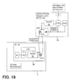
- FIGURE 19 illustrates transmitting and receiving RF signals between a contactless reader/writer (R/W) 90 and a contactless smart card or an RF ID tag 20 incorporated in an information processing apparatus 10 via respective coil antennas ANT, through magnetic coupling or transformer coupling.
- the reader/writer 90 transmits a carrier modulated with a command signal to the contactless smart card 20.
- the smart card 20 rectifies the modulated carrier signal to obtain driving power.
- the intensity of modulated magnetic field from the reader/writer 90 is sufficiently large, the power supply of the contactless smart card 20 is ON, and communications are initiated in response to a command provided by the reader/writer 90.
- the contactless smart card 20 does not provide a carrier signal, but modulates the modulated carrier signal magnetic field generated by the reader/writer 90 to send a command response or the like to the reader/writer 90.
- modulated carrier signal transmission and reception is usually done through magnetic coupling or transformer coupling via their planar coil antennas having large areas.
- a small-sized apparatus such as a notebook personal computer, a PDA or a cellular phone, is provided with electrical metal shields over its case and substrates, or over the components built in it in order to prevent undesired RF signals from radiating from the built-in components.
- a card or a reader/writer is incorporated into such an apparatus, the formation of magnetic field by the coil antennas is interfered and desirable communications cannot be achieved.
- a small-sized antenna device for electromagnetic wireless communications which can be built in a portable wireless apparatus.
- a small-sized antenna is formed of a grounded conductor, and a loop antenna is formed of straight or non-straight parallel portions and non-straight first and second rising portions, which loop antenna, together with the grounded conductor, forms the antenna device.
- An intermediate sheet of the card includes an insulating sheet having a set of two adjacent linear holes facing each other, an antenna coil formed by a conductor pattern formed on the opposing and side surfaces to wrap around the portion of the insulating sheet located between the linear holes, and an IC chip connected to the end terminals of the antenna coil.
- the intermediate sheet has its opposing surfaces covered with card-shaped resin or paper layers.
- a further solution may be to mount a coil antenna outside the case. This, however, causes an undesired protrusion to be formed on the case, which is disadvantageous in designing apparatus cases.
- a still further solution may be to dispose a sheet having high magnetic permeability between the case and the coil antenna so that a satisfactory magnetic field can be formed in the vicinity of the electric shield.
- high magnetic permeability sheets are expensive.
- the inventors have recognized that there is need for a coil antenna which is inexpensive, affects little the designing of a case of an apparatus, and can be built in the apparatus.
- An object of the invention is to provide a small coil antenna which can be housed in a small internal space of an apparatus.
- Another object of the invention is to provide an information processing apparatus with a coil antenna housed in a small internal space of the apparatus.
- a further object of the invention is to realize an information processing apparatus with a simple, inexpensive coil antenna.
- an information processing apparatus includes a case having an insulating casing, an electric shield disposed in the case, and a contactless reader and/or writer disposed in the case.
- the contactless reader and/or writer includes a transceiver disposed within the case for transmitting and/or receiving an RF modulated carrier signal, and a coil antenna having a plurality of conductor turns coupled to the transceiver and disposed in a space between the electric shield and the casing within the case, for transmitting and/or receiving an RF modulated carrier signal by magnetic coupling.
- the coil antenna includes a predetermined number of turns wound into a generally tubular shape about one center axis to have a predetermined length and a predetermined diameter.
- the coil antenna has a coil plane at one end of the predetermined length. No part of the electric shield is present between the coil plane and a part of the casing facing the coil plane on the one center axis.
- the coil antenna has its outer side spaced from the electric shield by a predetermined distance.
- a coil antenna for magnetic coupling is disposed on an insulating substrate having a given thickness.
- the coil antenna includes a plurality of turns wound about first and second axes crossing generally at a right angle to form an L-shape with one axis being perpendicular to a major surface of the substrate, over a continuous predetermined length along the first and second axes.
- the coil antenna has a first coil plane wound about the first axis at one end of the predetermined length.
- the coil antenna has a second coil plane wound about the second axis at the other end of the predetermined length.
- a small coil antenna can be housed in a small internal space of an apparatus, an information processing apparatus can have a coil antenna housed in a small internal space of the apparatus, and a simple, inexpensive coil antenna can be provided.
- FIGURES 1A through 1D each show a coil antenna 100 or 106 for a contactless reader/writer in accordance with embodiments of the present invention, which is disposed within a case or housing 10 of an information processing apparatus 2, such as a notebook personal computer, a PDA (Personal Digital Assistant) or a cellular phone, having an information entry or information presentation device 12, such as a liquid crystal display device, a keyboard or a key pad.
- an information processing apparatus 2 such as a notebook personal computer, a PDA (Personal Digital Assistant) or a cellular phone, having an information entry or information presentation device 12, such as a liquid crystal display device, a keyboard or a key pad.
- arrowed broken lines represent a magnetic flux generated by the coil antenna.
- the reader/writer 90 of the information processing apparatus 2 includes a transceiver 92 coupled to a CPU, and transmits and receives, by magnetic coupling or transformer coupling through its coil antenna ANT, RF signals to and from the contactless smart card or an RF ID tag 20 having a transceiver 24 and a coil antenna ANT coupled to the transceiver 24.
- the information processing apparatus 2 may be provided with another antenna for remote electromagnetic RF signal communications, such as mobile telephone communications and wireless LAN communications.
- coil antennas for RF signal transmission and reception by magnetic or transformer coupling are used for communications within a range of several tens of centimeters at the maximum, and are designed according to standards different from those for antennas for use in ordinary remote transmission and reception of electromagnetic RF signals.
- antennas for electromagnetic RF signal transmission and reception cannot be used in substitution for or in common as the magnetic or transformer coupling antennas.
- the case 10 shown in FIGURES 1A through 1D has a thin, generally parallelepiped shape having a broad major surface on which the information entry or presentation device 12 is disposed, but it is not limited to that shape but may have a different shape.
- an electric metal shield is provided in the case 10 to cover such a component.
- the reader/writer 90 may be disposed either outside or inside the electric shield.
- the coil antenna 100 or 106 in FIGURES 1A through 1D has a generally cylindrical outer shape with one center axis, and it includes plural turns, e.g. twenty (20) turns, so wound around the center axis to extend along a predetermined length thereof and have a predetermined diameter.
- the coil antennas 100 and 106 are disposed outward of the electric shield and inside an electrically nonconductive outer casing.
- the contactless smart card 20 is preferably disposed near the coil plane at an end of the coil antenna 100 or 106 in order to transmit and receive a modulated carrier to and from the reader/writer 90.
- the coil antenna 100 has a vertically extending center axis and is disposed in a recess at a location 50 along one side or a peripheral edge of a rectangular upper major surface of the case 10, with the upper and lower end coil planes of the coil antenna 100 located to face the upper and lower surface sides of the non-conductive outer casing of the case 10, respectively.
- the coil antenna 100 has a vertically extending center axis and is disposed in a recess in a corner 52 of the rectangular upper major surface of the case 10, with the upper and lower end coil planes of the coil antenna 100 located to face the upper and lower surface sides of the non-conductive outer casing of the case 10, respectively.
- the coil antenna 106 has a horizontally extending center axis and is disposed in a recess at the location 50 along one side or peripheral edge of the rectangular upper major surface of the case 10, with the left and right end coil planes of the coil antenna 106 located to face an outer surface side of the electric shield in the case 10 and a lateral side of the non-conductive outer casing of the case 10, respectively.
- the coil antenna 106 has a horizontally extending center axis and is disposed in the recess in the corner 52 of the rectangular upper major surface of the case 10, with the left and right end coil planes of the coil antenna 106 located to face the outer surface side of the electric shield in the case 10 and the lateral side of the non-conductive outer casing of the case 10, respectively.
- FIGURES 2A through 2C and 3 show other coil antennas 110, 114 and 120 for the contactless reader and/or writer 90 disposed within the casing 10 of the information processing apparatus 2 having the information entry or information presentation device 12, in accordance with other embodiments of the invention.
- Each of the coil antennas 110, 114 and 120 has a generally cylindrical outer shape having axes crossing each other generally at a right angle, and includes a plurality of turns, e.g. twenty (20) turns, wound continuously around the L-shaped, generally perpendicular two center axes along a predetermined length thereof.
- the arrangement of the remainder of the information processing apparatus 2 is the same as the apparatus shown in FIGURES 1A through 1D.
- the coil antenna 110 has two, vertically and horizontally extending center axes and is disposed in the recess at the location 50 along one side or peripheral edge of the rectangular upper major surface of the case 10, with the upper and right end coil planes of the coil antenna 110 located to face the upper and lateral sides of the non-conductive casing of the case 10, respectively.
- the coil antenna 110 has two, vertically and horizontally extending center axes and is disposed in the recess in the corner 52 of the rectangular upper major surface of the case 10, with the upper and right end coil planes of the coil antenna 110 located to face the upper and lateral sides of the non-conductive casing of the case 10, respectively.
- the two center axes cross at a right angle, but they need not cross exactly at a right angle.
- the coil antenna 114 has two, horizontal center axes extending in different directions and is disposed in the recess at the location 50 along one side or peripheral edge of the rectangular upper major surface of the case 10, with the front and right end coil planes of the coil antenna 114 located to face the front and lateral sides of the non-conductive casing of the case 10, respectively.
- the coil antenna 120 has two, vertically and horizontally extending center axes and is disposed in a recess at a location 60 of the rectangular upper major surface of the case 10, with the upper and right end coil planes about the two center axes of the coil antenna 120 located to face the upper side of the non-conductive outer casing of the case 10 and the right lateral side of such a recess of the electric shield, respectively.
- FIGURE 4A is a vertical cross-sectional view along a line 4A-4A through the case 10 shown in FIGURES 1A and 1B.
- FIGURE 4B is a vertical cross-sectional view along a line 4B-4B through the case 10 shown in FIGURE 1A.
- FIGURE 4C is a vertical cross-sectional view along a line 4C-4C through the case 10 shown in FIGURE 1B.
- FIGURES 4A and 4B show in detail how the coil antenna 100 of FIGURE 1A is disposed.
- FIGURES 4A and 4C show in detail how the coil antenna 100 of FIGURE 1B is disposed.
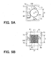
- FIGURES 5A and 5B are enlarged top plan and right-side views of the coil antenna 100 shown in FIGURE 1A or 1B, respectively, and show distances d S1 , d S2 and d s3 of the coil antenna 100 from outer surfaces 72, 73 and 74 of the electric shield 70 in FIGURES 4A through 4C. It should be noted that the case 10 of FIGURE 1B does not include the outer surface 74.
- the antenna 100 is disposed in the recess at the location 50 or 52, being spaced from the outer surface 72 facing an insulating substrate 80, of the electric shield 70 and one or two outer surfaces 73 and 74 generally perpendicular to the surface 72, by the distances d s1 , d s2 and d s3 , respectively.
- the coil antenna 100 has a center axis C1 and secured on the insulating substrate 80, formed of a material which does not exhibit high magnetic permeability, along a portion of a side or a side line portion S1 of the cylindrical coil along a length L, and the insulating substrate 80, in turn, is secured to the outer surface 72 of the electric shield 70.
- the coil antenna 100 has its coil plane P1 at one end of the cylindrical coil disposed inward of a non-conductive casing 78.
- the casing 78 is formed of, for example, plastic.
- no portion of the electric shield 70 is interposed between the portion of the casing 78 facing the coil plane P1 on the center axis C1 and the coil plane P1.
- a coil plane P2 at the other end of the cylindrical coil is disposed inward of the non-conductive casing 78 of the case 10.
- the reader/writer 90 reads from and/or writes into the contactless smart card 20.
- the length L of the coil antenna 100 along the center axis C1 is within a range of from 4.0 mm to 7.0 mm, preferably from 4.5 mm to 6.5 mm.
- the diameter or width D of the cross-section of the coil perpendicular to the center axis C1 is within a range of from 10 mm to 18 mm, preferably from 13 mm to 17 mm.
- the area A of the cross-section of the coil perpendicular to the center axis C1 is within a range of 70 mm 2 to 260 mm 2 , preferably from 120 mm 2 to 230 mm 2 .
- the distance between the coil antenna 100 and the non-conductive casing 78 can be 1 mm or less.
- the number of turns, N, of the coil antenna 100 is typically 6 or larger, preferably within a range of 16 to 25, and more preferably from 18 to 23. With the described arrangement, the coil antenna 100 can be mounted in a small recess within the case 10, which does not require an undesirable large space for the coil antenna 100 in the case 10 so that the degree of freedom in designing the case 10 can increase.
- FIGURE 6A is a vertical cross-sectional view along a line 6A-6A through the case 10 shown in FIGURE 1C or 1D.
- FIGURE 6B is a vertical cross-sectional view along a line 6B-6B through the case 10 shown in FIGURE 1C.
- FIGURE 6C is a vertical cross-sectional view along a line 6C-6C through the case 10 shown in FIGURE 1D.
- FIGURES 6A and 6B show in detail how the coil antenna 106 of FIGURE 1C is disposed.
- FIGURES 6A and 6C show in detail how the coil antenna 106 of FIGURE 1D is disposed.
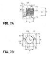
- FIGURES 7A and 7B are enlarged top plan and right side views of the coil antenna 106 shown in FIGURE 1C or 1D, respectively, and show distances d B , d S2 and d S3 of the coil antenna 106 from outer surfaces 72, 73 and 74 of the electric shield 70 in FIGURES 6A through 6C. It should be noted that the case 10 of FIGURE 1D does not include the outer surface 74.
- the coil antenna 106 is disposed in the recess at the locations 50 and 52, being spaced from the outer surface 72 of the electric shield 70 facing the insulating substrate 80, and the outer surfaces 73 and 74 extending generally perpendicularly to the outer surface 72, by the distances d B , d S2 and d S3 , respectively.
- the coil antenna 106 has the center axis C1 and has its coil plane P1 at one end of the cylindrical coil disposed inward of the non-conductive casing 78 of the case 10.
- the coil antenna 106 has its coil plane P2 at the other end of the cylindrical coil secured on the insulating substrate 80 formed of a material which does not exhibit high magnetic permeability, and the insulating substrate 80 is secured to the outer surface 72 of the electric shield 70.
- the outer surface 72 of the electric shield 70 is spaced from the other coil plane P2 on the center axis C1 by the predetermined distance d B .
- 1.5 mm or larger is sufficient for the distances d B , and, typically, it is in a range of from 1.5 mm to 6.0 mm, preferably from 1.5 mm to 3.5 mm, and more preferably from 2.0 mm to 3.0 mm.
- the other dimensions and features of the coil antenna 106 are same as those of the coil antenna 100.
- each of the antennas 100 and 106, along the center axis C1 is generally a quarter or one-third or larger of the diameter or width D of the respective coils, so that the area A of the coil plane can be small relative to a conventional planar antenna whose length along the center axis thereof is substantially 0 (zero).
- Each of the coil antennas 100 and 106 has a total length of the coil conductor somewhat longer than that of a conventional planar coil antenna, and has a larger number of turns, N, than that of the conventional planar coil antenna, whereby a magnetic field or flux is comparable to the magnetic field or flux provided by the conventional planar coil antenna can be produced.
- the coil antenna 100 or 106 When the coil antenna 100 or 106 is used, it is not always necessary to interpose a material having high magnetic permeability between the electric shield 70 of the case 10 and the coil, which leads to substantial reduction of the manufacturing cost. For example, even when a material of high magnetic permeability, e.g. a ferrite sheet, is interposed, the amount of the necessary high magnetic permeability material can be small because the areas of the coil planes at both of the opposite ends of each of the coil antennas 100 and 106 are small.
- a material of high magnetic permeability e.g. a ferrite sheet
- FIGURE 8A is a vertical cross-sectional view along a line 8A-8A through the case 10 shown in FIGURES 2A and 2B.
- FIGURE 8B is a vertical cross-sectional view along a line 8B-8B through the case 10 shown in FIGURE 2A.
- FIGURE 8C is a vertical cross-sectional view along a line 8C-8C through the case 10 shown in FIGURE 2B.
- FIGURES 8A and 8B show in detail how the coil antenna 110 of FIGURE 2A is disposed.
- FIGURES 8A and 8C show in detail how the coil antenna 110 of FIGURE 2B is disposed.
- FIGURE 9A is a vertical cross-sectional view along a line 9A-9A through the case 10 shown in FIGURE 2C.
- FIGURE 9B is a vertical cross-sectional view along a line 9B-9B through the case 10 shown in FIGURE 2C.
- FIGURES 9A and 9B show in detail how the coil antenna 114 of FIGURE 2C is disposed.
- FIGURE 10 is a vertical cross-sectional view along a line 10-10 through the case 10 shown in FIGURE 3.
- FIGURE 10 shows in detail how the coil antenna 120 is disposed.
- FIGURE 11 is an enlarged view of FIGURES 2A through 2C and 3, and shows distances d S1 , d S2 and d B of the coil antennas 110, 114 and 120 shown in FIGURES 2A through 2C and 3 from the outer surfaces 72, 73 and 74 of the electric shield 70.
- FIGURE 11 corresponds to the upside-down version of the antenna 110 shown in FIGURES 2A and 2B, to the top plan view of the coil antenna 114 of FIGURE 2C, and to the version of the coil antenna 120 of FIGURE 3 turned clockwise by 90°, that the case 10 of FIGURES 2A and 2B does not have the outer surfaces 73 and 74, and that the case 10 of FIGURE 2C does not have the outer surface 74.
- Each of the coil antennas 110, 114 and 120 has center axes C1 and C2.
- a portion S3 of the side surface or line of the cylindrical coil, which is generally parallel to one of the center axes, C2, of each coil antenna is secured along a predetermined length L s to the insulating substrate 80 made of a material which does not exhibit high magnetic permeability, and the insulating substrate 80 is secured to the outer surface 72 of the electric shield 70.
- Each of the coil antennas 110, 114 and 120 is disposed in such a manner that at least the coil plane P1 at one end thereof on the center axis C1 faces the inner surface of the non-conductive casing 78 of the case 10.
- the electric shield 70 does not have any portion interposed between the coil plane P1 and the part of the casing 78 facing the coil plane P1 on the center axis C1.
- each of the coil antennas 110 and 114 is disposed in such a manner that the coil plane P2 at the other end of the cylindrical coil faces to the inner surface of the non-conductive casing of the case 10.
- the coil antenna 120 is disposed in such a manner that the coil plane P2 at the other end of the cylindrical coil faces the outer surface 74 of the electric shield 70.
- Each of the coil antennas 110, 114 and 120 is disposed in the recess at the location 50, 52 or 60, being spaced from the outer surface 72 of the electric shield 70 facing the insulating substrate 80 and from either or both of the outer surfaces 73 and 74 generally perpendicular to the outer surface 72, by the distances d S1 , d S2 and d B .
- About 1.5 mm or larger is sufficient for the distance d B , and it is typically within a range of from 1.5 mm to 6.0 mm, preferably within a range of from 1.5 mm to 3.5 mm, and more preferably within a range of from 2.0 mm to 3.0 mm.
- About 1 mm or larger is sufficient for each of the distances d S1 and d S2 .
- each of the distances d S1 and d S2 is typically within a range of from 1 mm to 6 mm, preferably within a range of from 1.5 mm to 3.5 mm, and more preferably within a range of from 2.0 mm to 3.0 mm.
- the total length L1 + L2 along the generally perpendicular center axes C1 and C2 of each of the coil antennas 110, 114 and 120 corresponds to the aforementioned length L, which is typically within a range of from 4.0 mm to 7.0 mm, and preferably within a range of from 4.5 mm to 6.5 mm.
- the diameter or width D of the coil in the cross-section perpendicular to each of the center axes C1 and C2 is typically within a range of from 10 mm to 18 mm, and preferably within a range of from 13 mm to 17 mm.
- the area A of the cross-section of the coil perpendicular to each of the center axes C1 and C2 is within a range of from 70 mm 2 to 260 mm 2 , preferably within a range of from 120 mm 2 to 230 mm 2 .
- the total number of turns, N1 + N2, of each of the coil antennas 110, 114 and 120 is typically 6 or larger, preferably within a range of from 17 to 24.
- the other dimensions, geometries and features of the coil antennas 110, 114 and 120 are the same as those of the coil antennas 100 and 106.
- FIGURE 12 shows a coil antenna 126 in accordance with a still further embodiment of the invention, for use in the contactless reader and/or writer 90 which is mounted at the location 60 shown in FIGURE 3 of the case 10 of the information processing apparatus 2.
- the coil antenna 126 is disposed in a recess at the location 60 shown in FIGURE 3.
- the coil antenna 126 has the same shape as the coil antenna 106 of FIGURE 1C, but the coil plane at one end and the entire outer side surface of the coil antenna 126 are surrounded with the electric shield 70.
- a sheet 84 of high magnetic permeability having a small area is disposed between the coil plane of the coil antenna 126 and the insulating substrate 80.
- the coil antenna 126 has a larger length L and a larger number of turns, N, than a conventional planar coil antenna, while the area A of the coil plane is small, and hence the area of the high magnetic permeability material sheet 84 can be small.
- the use of the high magnetic permeability material sheet 84 can further reduce the distance d B between the lower end coil plane of the coil antenna 126 and the outer surface 72 of the electric shield 70.
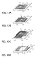
- FIGURES 13A through 13D show different structures of coil antennas 122-125 wound into a generally rectangular shape in accordance with still further embodiments of the invention.
- the coil antenna 122 has an L-shaped structure similar to the coil antennas 110, 114 and 120 shown in FIGURES 2A through 2C and 3.
- the coil antenna 122 has center axes C1 and C2 crossing generally at a right angle to form an L-shape, and a coil conductor 132 is wound slantwise in a number of turns, N2, around an insulating plate 140 through which the center axis C2 passes, with the slope of the conductor becoming gradually gentler as the winding gets close to the center axis C1, and a coil conductor 134 is wound in a number of turns, N1, on the surface of the insulating plate 140 about the center axis C1 extending perpendicular to the surface of the insulating plate 140.
- the coil antenna 123 is branched into a T-shape.
- the coil antenna 123 has center axes C1 and C2 crossing generally at a right angle to form a T-shape.
- the coil conductor 132 is wound slantwise in a plurality of turns, N2, about the insulating plate 140 through which the center axis C2 passes, with the slope of the conductor becoming gradually gentler as the winding gets close to the center axis C1, and the coil conductor 134 is wound on the surface of the insulating plate 140 in a plurality of turns, N1, about the center axis C1 perpendicular to this surface.
- a coil conductor 136 is wound slantwise in a plurality of turns, N3, about the insulating plate 140 through which the center axis C2 passes, with the slope of the conductor becoming gradually gentler as the winding gets close to the center axis C1.
- the directions in which the respective conductors are wound are such that magnetic fluxes or fields of the same magnetic polarity can be generated in the direction indicated by dashed arrows.
- the coil antenna 124 branches into three axial directions.
- the coil antenna 124 has center axes C1, C2 and C3 crossing generally at right angles.
- the coil conductor 132 is wound slantwise in a plurality of turns, N2, about the insulating plate 140 through which the center axis C1 passes, with the slope of the conductor becoming gradually gentler as the winding gets close to the center axis C1.
- the coil conductor 134 is a plurality of turns, N1, on the insulating plate 140 about the center axis C1.
- the coil conductor 136 is wound slantwise in a plurality, N3, of turns about the insulating plate 140 through which the center axis C3 passes, with the slope of the conductor becoming gradually gentler as the winding gets close to the center axis C1.
- the coil antenna 125 has center axes C1 and C2 crossing generally at a right angle.
- the coil conductor 132 is wound slantwise in plural turns about the insulating plate 140 through which the center axis C2 passes, with the slope of the conductor becoming gradually gentler as the winding gets close to the center axis C1.
- the coil conductor 136 is wound slantwise in plural turns in the opposite direction about the insulating plate 140 through which the center axis C2 passes, with the slope of the conductor becoming gradually gentler as the winding gets close to the center axis C1.
- each of the coil antennas 100, 106, 110, 114, 120, 126 and 132 as described above may be formed of multiple layered substrates with a planar coil formed on each substrate and with the planar coils connected in series.
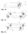
- FIGURE 14 shows coil antennas 100 and 101 disposed at two close locations 50 and 51 near one side or periphery of the rectangular upper major surface of the case 10.
- the contactless smart card 20 is placed near to end coil planes of the two coil antennas 100 and 101, whereby the magnetic field coupled between the coil antennas 100 and 101 of the reader/writer 90 and the coil antenna of the contactless smart card 20 is further enhanced, so that the signal transmission and reception between the reader/writer 90 and the contactless smart card 20 can be further ensured.
- FIGURE 15 shows four coil antennas 106, 107, 108 and 109, each having a horizontally extending center axis, disposed in recesses respectively in four corners 52, 53, 54 and 55 of the rectangular upper major surface of the case 10.
- the contactless smart card 20 is placed close to one end coil plane of any of the four coil antennas 106, 107, 108 and 109, whereby the degree of freedom of placing the contactless smart card 20 increases.
- the coil antennas e.g. the coil antennas 106 and 107, may be disposed so as to surround respective bolts 152 used to secure the casing 78 of the case 10, whereby the inner space for housing the coil antennas 106 and 107 can be more easily secured.
- FIGURE 16 shows four coil antennas 100, 101, 102 and 103, each having a vertically extending center axis, disposed in recesses respectively in the four corners 52, 53, 54 and 55 of the rectangular upper major surface of the case 10.
- the four corners of the contactless smart card 20 can be located near respective one end coil planes of the four coil antennas 100, 101, 102 and 103, whereby the magnetic field coupled between the coil antennas 100, 101, 102 and 103 of the reader/writer 90 and the coil antenna of the contactless smart card 20 can be enhanced, so that the signal transmission and reception between the reader/writer 90 and the contactless smart card 20 can be further ensured.
- the coil antennas e.g. the coil antennas 100 and 101, may be disposed to surround the respective bolts 152 used to secure the casing 78 of the case 10, whereby the inner space for housing the coil antennas 100 and 101 can be more easily secured.
- FIGURE 17 shows a notebook personal computer 14 with the coil antenna 100 mounted in the top end portion of a display case 16 functioning as the case 10.
- the display case 16 includes a card holder 22 on its exterior surface in the vicinity of the coil plane at one end of the coil antenna 100, whereby the position where the contactless smart card 20 is to be placed can be indicated, and the magnetic coupling between the coil antenna 100 and the coil antenna of the contactless card 20 can be ensured.
- FIGURES 18A through 18D show antenna units 290, 292, 294 and 296, respectively, which are mounted along one side of a rectangular upper major surface in an information processing apparatus 270.
- the antenna unit 290 includes a coil antenna 192 having a plurality of cylindrical coil sections with parallel, horizontally extending center axes, disposed in parallel and connected in series.
- the antenna unit 292 includes a coil antenna 194 wound around a single, horizontally extending center axis into a shape of a hollow parallelepiped.
- the antenna unit 294 includes a coil antenna 196 having a plurality of cylindrical coil sections with parallel, vertically extending center axes, disposed in parallel and connected in series.
- the antenna unit 296 includes a coil antenna 198 wound around a single, vertically extending center axis into a shape of an oval cylinder.
- the information processing apparatus 270 may be the small-sized information processing apparatus 2 including the contactless reader/writer 90 or the contactless smart card 20.
- the antenna coil plane can be made smaller, which enables the area of the outer surface 72 of the electric shield 70 recessed from the casing 78 to be smaller, e.g. to an area on the order of 17 mm x 17 mm. This leads to minimization of the area of the high magnetic permeability sheet.
Landscapes
- Engineering & Computer Science (AREA)
- Physics & Mathematics (AREA)
- Toxicology (AREA)
- General Physics & Mathematics (AREA)
- Theoretical Computer Science (AREA)
- Health & Medical Sciences (AREA)
- Computer Vision & Pattern Recognition (AREA)
- Computer Networks & Wireless Communication (AREA)
- Artificial Intelligence (AREA)
- Electromagnetism (AREA)
- General Health & Medical Sciences (AREA)
- Computer Hardware Design (AREA)
- Microelectronics & Electronic Packaging (AREA)
- Signal Processing (AREA)
- Near-Field Transmission Systems (AREA)
- Details Of Aerials (AREA)
- Support Of Aerials (AREA)
- Variable-Direction Aerials And Aerial Arrays (AREA)
Abstract
Description
- The present invention relates generally to an apparatus for reading from and/or writing into a contactless smart card and an RF ID tag, and, more particularly, to a structure and arrangement of a coil antenna for use in reading from and writing into a contactless smart card and an RF ID tag.
- Recently, a contactless reader and/or writer (hereinafter sometimes referred to simply as reader/writer) for reading from and writing into a contactless smart card or contactless IC card, and an RF ID tag, has been used widely more and more. A contactless smart card is used, for example, for supervision of entry into and exit from a room, personal identification, traffic ticketing and electronic money. An RF ID tag is used, for example, in commodity management, room entry and exit supervision, and physical distribution management. Also, PAN (Personal Area Network) communications using contactless smart cards and RF ID tags have been proposed. It is expected that such a reader/writer will be incorporated into small-sized information processing apparatuses, such as personal computers, PDAs and cellular phones. It is also expected that contactless smart card and RF ID tag functions will be incorporated into mobile apparatuses, such as PDAs and cellular phones.
- FIGURE 19 illustrates transmitting and receiving RF signals between a contactless reader/writer (R/W) 90 and a contactless smart card or an
RF ID tag 20 incorporated in aninformation processing apparatus 10 via respective coil antennas ANT, through magnetic coupling or transformer coupling. The reader/writer 90 transmits a carrier modulated with a command signal to the contactlesssmart card 20. Thesmart card 20 rectifies the modulated carrier signal to obtain driving power. When the intensity of modulated magnetic field from the reader/writer 90 is sufficiently large, the power supply of the contactlesssmart card 20 is ON, and communications are initiated in response to a command provided by the reader/writer 90. The contactlesssmart card 20 does not provide a carrier signal, but modulates the modulated carrier signal magnetic field generated by the reader/writer 90 to send a command response or the like to the reader/writer 90. Such modulated carrier signal transmission and reception is usually done through magnetic coupling or transformer coupling via their planar coil antennas having large areas. - For communications between the contactless
smart card 20 and the reader/writer 90, the magnetic environments of the coil antennas of both of them must be good. A small-sized apparatus, such as a notebook personal computer, a PDA or a cellular phone, is provided with electrical metal shields over its case and substrates, or over the components built in it in order to prevent undesired RF signals from radiating from the built-in components. Thus, when a card or a reader/writer is incorporated into such an apparatus, the formation of magnetic field by the coil antennas is interfered and desirable communications cannot be achieved. - Saito disclosed, in Japanese Patent Application Publication JP 2001-284935-A published on October 12, 2001, a small-sized antenna device for electromagnetic wireless communications which can be built in a portable wireless apparatus. A small-sized antenna is formed of a grounded conductor, and a loop antenna is formed of straight or non-straight parallel portions and non-straight first and second rising portions, which loop antenna, together with the grounded conductor, forms the antenna device.
- In Japanese Patent Application Publication JP HEI 11-213116-A published on August 6, 1999, Yamamoto et al. disclosed a contactless smart card which is resistant to bending, easy to produce and free of electric field disturbance. An intermediate sheet of the card includes an insulating sheet having a set of two adjacent linear holes facing each other, an antenna coil formed by a conductor pattern formed on the opposing and side surfaces to wrap around the portion of the insulating sheet located between the linear holes, and an IC chip connected to the end terminals of the antenna coil. The intermediate sheet has its opposing surfaces covered with card-shaped resin or paper layers.
- In order for the coil antenna ANT of the reader/
writer 90 of FIGURE 19 to produce a satisfactory magnetic field, influence of the electrical shields on the coil antennas of both of the contactlesssmart card 20 and the reader/writer'90 need be eliminated. As one solution, an area of the electric shield of the case corresponding to the size of the coil antennas may be removed, which, however, causes insufficient prevention of an undesired RF signal generated in the apparatus from being radiated. Another solution may be to provide a large distance between the electric shield of the case and the coil antenna, which, however, forms an undesirable space between the coil antennas and the electric shield. This is disadvantageous in designing cases for apparatuses, in particular, cases for, e.g. PDAs and cellular phones, which are desired to be minimized in size. A further solution may be to mount a coil antenna outside the case. This, however, causes an undesired protrusion to be formed on the case, which is disadvantageous in designing apparatus cases. A still further solution may be to dispose a sheet having high magnetic permeability between the case and the coil antenna so that a satisfactory magnetic field can be formed in the vicinity of the electric shield. However, high magnetic permeability sheets are expensive. - The inventors have recognized that there is need for a coil antenna which is inexpensive, affects little the designing of a case of an apparatus, and can be built in the apparatus.
- An object of the invention is to provide a small coil antenna which can be housed in a small internal space of an apparatus.
- Another object of the invention is to provide an information processing apparatus with a coil antenna housed in a small internal space of the apparatus.
- A further object of the invention is to realize an information processing apparatus with a simple, inexpensive coil antenna.
- In accordance with an aspect of the present invention, an information processing apparatus includes a case having an insulating casing, an electric shield disposed in the case, and a contactless reader and/or writer disposed in the case. The contactless reader and/or writer includes a transceiver disposed within the case for transmitting and/or receiving an RF modulated carrier signal, and a coil antenna having a plurality of conductor turns coupled to the transceiver and disposed in a space between the electric shield and the casing within the case, for transmitting and/or receiving an RF modulated carrier signal by magnetic coupling. The coil antenna includes a predetermined number of turns wound into a generally tubular shape about one center axis to have a predetermined length and a predetermined diameter. The coil antenna has a coil plane at one end of the predetermined length. No part of the electric shield is present between the coil plane and a part of the casing facing the coil plane on the one center axis. The coil antenna has its outer side spaced from the electric shield by a predetermined distance.
- In accordance with another embodiment of the invention, a coil antenna for magnetic coupling is disposed on an insulating substrate having a given thickness. The coil antenna includes a plurality of turns wound about first and second axes crossing generally at a right angle to form an L-shape with one axis being perpendicular to a major surface of the substrate, over a continuous predetermined length along the first and second axes. The coil antenna has a first coil plane wound about the first axis at one end of the predetermined length. The coil antenna has a second coil plane wound about the second axis at the other end of the predetermined length.
- According to the invention, a small coil antenna can be housed in a small internal space of an apparatus, an information processing apparatus can have a coil antenna housed in a small internal space of the apparatus, and a simple, inexpensive coil antenna can be provided.
- The invention will be described in connection with embodiments with reference to the accompanying drawings. Throughout the drawings, similar symbols and numerals indicate similar items and functions.
-
- FIGURES 1A through 1D each show a coil antenna for a contactless reader and/or writer in accordance with an embodiment of the present invention, which is disposed within a case of an information processing apparatus having an information entry or information presentation area;
- FIGURES 2A through 2C show other coil antennas for the contactless reader and/or writer disposed within the casing of the information processing apparatus having the information entry or information presentation device, in accordance with other embodiments of the invention;
- FIGURE 3 show a further coil antennas for the contactless reader and/or writer disposed within the casing of the information processing apparatus having the information entry or information presentation device, in accordance with further embodiments of the invention;
- FIGURE 4A is a vertical cross-sectional view along a
line 4A-4A through the case shown in FIGURES 1A and 1B, FIGURE 4B is a vertical cross-sectional view along aline 4B-4B through the case shown in FIGURE 1A, and FIGURE 4C is a vertical cross-sectional view along aline 4C-4C through the case shown in FIGURE 1B; - FIGURES 5A and 5B are enlarged top plan and right-side views of the coil antenna shown in FIGURE 1A or 1B, respectively, and show distances of the coil antenna from outer surfaces of the electric shield in FIGURES 4A through 4C;
- FIGURE 6A is a vertical cross-sectional view along a
line 6A-6A through the case shown in FIGURE 1C or 1D; - FIGURE 6B is a vertical cross-sectional view along a
line 6B-6B through the case shown in FIGURE 1C; - FIGURE 6C is a vertical cross-sectional view along a
line 6C-6C through the case shown in FIGURE 1D; - FIGURES 7A and 7B are enlarged top plan and right side views of the coil antenna shown in FIGURE 1C or 1D, respectively, and show distances of the coil antenna from outer surfaces of the electric shield in FIGURES 6A through 6C;
- FIGURE 8A is a vertical cross-sectional view along a
line 8A-8A through the case shown in FIGURES 2A and 2B; - FIGURE 8B is a vertical cross-sectional view along a
line 8B-8B through the case shown in FIGURE 2A; - FIGURE 8C is a vertical cross-sectional view along a
line 8C-8C through the case shown in FIGURE 2B; - FIGURE 9A is a vertical cross-sectional view along a
line 9A-9A through the case shown in FIGURE 2C; - FIGURE 9B is a vertical cross-sectional view along a
line 9B-9B through the case shown in FIGURE 2C; - FIGURE 10 is a vertical cross-sectional view along a line 10-10 through the case shown in FIGURE 3;
- FIGURE 11 is an enlarged view of FIGURES 2A through 2C and 3, and shows distances of the coil antennas shown in FIGURES 2A through 2C and 3 from the outer surfaces of the electric shield;
- FIGURE 12 shows a coil antenna in accordance with a still further embodiment of the invention, for use in the contactless reader and/or writer which is mounted at the location shown in FIGURE 3 of the case of the information processing apparatus;
- FIGURES 13A through 13D show different structures of coil antennas wound into a generally rectangular shape in accordance with still further embodiments of the invention;
- FIGURE 14 shows coil antennas disposed at two close locations near one side or periphery of the rectangular upper major surface of the case;
- FIGURE 15 shows four coil antennas, each having a horizontally extending center axis, disposed in recesses respectively in four corners of the rectangular upper major surface of the case;
- FIGURE 16 shows four coil antennas, each having a vertically extending center axis, disposed in recesses respectively in the four corners of the rectangular upper major surface of the case;
- FIGURE 17 shows a notebook personal computer with the coil antenna mounted in the top end portion of a display case functioning as the case;
- FIGURES 18A through 18D show antenna units, respectively, which are mounted along one side of a rectangular upper major surface in an information processing apparatus; and
- FIGURE 19 illustrates transmitting and receiving RF signals between a contactless reader/writer and a contactless smart card or an RF ID tag incorporated in an information processing apparatus via respective coil antennas, through magnetic or transformer coupling.
- FIGURES 1A through 1D each show a
coil antenna housing 10 of aninformation processing apparatus 2, such as a notebook personal computer, a PDA (Personal Digital Assistant) or a cellular phone, having an information entry orinformation presentation device 12, such as a liquid crystal display device, a keyboard or a key pad. In the figures, arrowed broken lines represent a magnetic flux generated by the coil antenna. - Referring to FIGURE 19, the reader/
writer 90 of theinformation processing apparatus 2 includes atransceiver 92 coupled to a CPU, and transmits and receives, by magnetic coupling or transformer coupling through its coil antenna ANT, RF signals to and from the contactless smart card or anRF ID tag 20 having atransceiver 24 and a coil antenna ANT coupled to thetransceiver 24. Alternatively, theinformation processing apparatus 2 may be provided with another antenna for remote electromagnetic RF signal communications, such as mobile telephone communications and wireless LAN communications. Usually, coil antennas for RF signal transmission and reception by magnetic or transformer coupling are used for communications within a range of several tens of centimeters at the maximum, and are designed according to standards different from those for antennas for use in ordinary remote transmission and reception of electromagnetic RF signals. Thus antennas for electromagnetic RF signal transmission and reception cannot be used in substitution for or in common as the magnetic or transformer coupling antennas. - The
case 10 shown in FIGURES 1A through 1D has a thin, generally parallelepiped shape having a broad major surface on which the information entry orpresentation device 12 is disposed, but it is not limited to that shape but may have a different shape. In order to prevent undesired RF signal radiation from a component, such as a microprocessor or a hard disc driver, within thecase 10, an electric metal shield is provided in thecase 10 to cover such a component. The reader/writer 90 may be disposed either outside or inside the electric shield. - The
coil antenna coil antennas smart card 20 is preferably disposed near the coil plane at an end of thecoil antenna writer 90. - In FIGURE 1A, the
coil antenna 100 has a vertically extending center axis and is disposed in a recess at alocation 50 along one side or a peripheral edge of a rectangular upper major surface of thecase 10, with the upper and lower end coil planes of thecoil antenna 100 located to face the upper and lower surface sides of the non-conductive outer casing of thecase 10, respectively. - In FIGURE 1B, the
coil antenna 100 has a vertically extending center axis and is disposed in a recess in acorner 52 of the rectangular upper major surface of thecase 10, with the upper and lower end coil planes of thecoil antenna 100 located to face the upper and lower surface sides of the non-conductive outer casing of thecase 10, respectively. - In FIGURE 1C, the
coil antenna 106 has a horizontally extending center axis and is disposed in a recess at thelocation 50 along one side or peripheral edge of the rectangular upper major surface of thecase 10, with the left and right end coil planes of thecoil antenna 106 located to face an outer surface side of the electric shield in thecase 10 and a lateral side of the non-conductive outer casing of thecase 10, respectively. - In FIGURE 1D, the
coil antenna 106 has a horizontally extending center axis and is disposed in the recess in thecorner 52 of the rectangular upper major surface of thecase 10, with the left and right end coil planes of thecoil antenna 106 located to face the outer surface side of the electric shield in thecase 10 and the lateral side of the non-conductive outer casing of thecase 10, respectively. - FIGURES 2A through 2C and 3 show
other coil antennas writer 90 disposed within thecasing 10 of theinformation processing apparatus 2 having the information entry orinformation presentation device 12, in accordance with other embodiments of the invention. Each of thecoil antennas information processing apparatus 2 is the same as the apparatus shown in FIGURES 1A through 1D. - In FIGURE 2A, the
coil antenna 110 has two, vertically and horizontally extending center axes and is disposed in the recess at thelocation 50 along one side or peripheral edge of the rectangular upper major surface of thecase 10, with the upper and right end coil planes of thecoil antenna 110 located to face the upper and lateral sides of the non-conductive casing of thecase 10, respectively. - In FIGURE 2B, the
coil antenna 110 has two, vertically and horizontally extending center axes and is disposed in the recess in thecorner 52 of the rectangular upper major surface of thecase 10, with the upper and right end coil planes of thecoil antenna 110 located to face the upper and lateral sides of the non-conductive casing of thecase 10, respectively. - It is preferable that the two center axes cross at a right angle, but they need not cross exactly at a right angle.
- In FIGURE 2C, the
coil antenna 114 has two, horizontal center axes extending in different directions and is disposed in the recess at thelocation 50 along one side or peripheral edge of the rectangular upper major surface of thecase 10, with the front and right end coil planes of thecoil antenna 114 located to face the front and lateral sides of the non-conductive casing of thecase 10, respectively. - In FIGURE 3, the
coil antenna 120 has two, vertically and horizontally extending center axes and is disposed in a recess at alocation 60 of the rectangular upper major surface of thecase 10, with the upper and right end coil planes about the two center axes of thecoil antenna 120 located to face the upper side of the non-conductive outer casing of thecase 10 and the right lateral side of such a recess of the electric shield, respectively. - FIGURE 4A is a vertical cross-sectional view along a
line 4A-4A through thecase 10 shown in FIGURES 1A and 1B. FIGURE 4B is a vertical cross-sectional view along aline 4B-4B through thecase 10 shown in FIGURE 1A. FIGURE 4C is a vertical cross-sectional view along aline 4C-4C through thecase 10 shown in FIGURE 1B. FIGURES 4A and 4B show in detail how thecoil antenna 100 of FIGURE 1A is disposed. FIGURES 4A and 4C show in detail how thecoil antenna 100 of FIGURE 1B is disposed. - FIGURES 5A and 5B are enlarged top plan and right-side views of the
coil antenna 100 shown in FIGURE 1A or 1B, respectively, and show distances dS1, dS2 and ds3 of thecoil antenna 100 fromouter surfaces electric shield 70 in FIGURES 4A through 4C. It should be noted that thecase 10 of FIGURE 1B does not include theouter surface 74. - The
antenna 100 is disposed in the recess at thelocation outer surface 72 facing an insulatingsubstrate 80, of theelectric shield 70 and one or twoouter surfaces surface 72, by the distances ds1, ds2 and ds3, respectively. Thecoil antenna 100 has a center axis C1 and secured on the insulatingsubstrate 80, formed of a material which does not exhibit high magnetic permeability, along a portion of a side or a side line portion S1 of the cylindrical coil along a length L, and the insulatingsubstrate 80, in turn, is secured to theouter surface 72 of theelectric shield 70. Thecoil antenna 100 has its coil plane P1 at one end of the cylindrical coil disposed inward of anon-conductive casing 78. Thecasing 78 is formed of, for example, plastic. In other words, no portion of theelectric shield 70 is interposed between the portion of thecasing 78 facing the coil plane P1 on the center axis C1 and the coil plane P1. Similarly, a coil plane P2 at the other end of the cylindrical coil is disposed inward of thenon-conductive casing 78 of thecase 10. - When the contactless
smart card 20 is disposed on a portion of thecasing 78 near the one end coil plane P1, the reader/writer 90 reads from and/or writes into the contactlesssmart card 20. - About 1 mm or larger is sufficient for each of the distances dS1, dS2 and dS3, and, typically, they are each within a range of from 1 mm to 6 mm for the small inner space or recess in the
case 10 of theinformation processing apparatus 2, preferably from 1.5 mm to 3.5 mm, and more preferably from 2.0 mm to 3.0 mm. The length L of thecoil antenna 100 along the center axis C1 is within a range of from 4.0 mm to 7.0 mm, preferably from 4.5 mm to 6.5 mm. The diameter or width D of the cross-section of the coil perpendicular to the center axis C1 is within a range of from 10 mm to 18 mm, preferably from 13 mm to 17 mm. The area A of the cross-section of the coil perpendicular to the center axis C1 is within a range of 70 mm2 to 260 mm2, preferably from 120 mm2 to 230 mm2. The distance between thecoil antenna 100 and thenon-conductive casing 78 can be 1 mm or less. The number of turns, N, of thecoil antenna 100 is typically 6 or larger, preferably within a range of 16 to 25, and more preferably from 18 to 23. With the described arrangement, thecoil antenna 100 can be mounted in a small recess within thecase 10, which does not require an undesirable large space for thecoil antenna 100 in thecase 10 so that the degree of freedom in designing thecase 10 can increase. - FIGURE 6A is a vertical cross-sectional view along a
line 6A-6A through thecase 10 shown in FIGURE 1C or 1D. FIGURE 6B is a vertical cross-sectional view along aline 6B-6B through thecase 10 shown in FIGURE 1C. FIGURE 6C is a vertical cross-sectional view along aline 6C-6C through thecase 10 shown in FIGURE 1D. FIGURES 6A and 6B show in detail how thecoil antenna 106 of FIGURE 1C is disposed. FIGURES 6A and 6C show in detail how thecoil antenna 106 of FIGURE 1D is disposed. - FIGURES 7A and 7B are enlarged top plan and right side views of the
coil antenna 106 shown in FIGURE 1C or 1D, respectively, and show distances dB, dS2 and dS3 of thecoil antenna 106 fromouter surfaces electric shield 70 in FIGURES 6A through 6C. It should be noted that thecase 10 of FIGURE 1D does not include theouter surface 74. - The
coil antenna 106 is disposed in the recess at thelocations outer surface 72 of theelectric shield 70 facing the insulatingsubstrate 80, and theouter surfaces outer surface 72, by the distances dB, dS2 and dS3, respectively. Thecoil antenna 106 has the center axis C1 and has its coil plane P1 at one end of the cylindrical coil disposed inward of thenon-conductive casing 78 of thecase 10. Thecoil antenna 106 has its coil plane P2 at the other end of the cylindrical coil secured on the insulatingsubstrate 80 formed of a material which does not exhibit high magnetic permeability, and the insulatingsubstrate 80 is secured to theouter surface 72 of theelectric shield 70. In other words, theouter surface 72 of theelectric shield 70 is spaced from the other coil plane P2 on the center axis C1 by the predetermined distance dB. - About 1.5 mm or larger is sufficient for the distances dB, and, typically, it is in a range of from 1.5 mm to 6.0 mm, preferably from 1.5 mm to 3.5 mm, and more preferably from 2.0 mm to 3.0 mm. The other dimensions and features of the
coil antenna 106 are same as those of thecoil antenna 100. - The length L of each of the
antennas coil antennas coil antenna electric shield 70 of thecase 10 and the coil, which leads to substantial reduction of the manufacturing cost. For example, even when a material of high magnetic permeability, e.g. a ferrite sheet, is interposed, the amount of the necessary high magnetic permeability material can be small because the areas of the coil planes at both of the opposite ends of each of thecoil antennas - FIGURE 8A is a vertical cross-sectional view along a
line 8A-8A through thecase 10 shown in FIGURES 2A and 2B. FIGURE 8B is a vertical cross-sectional view along aline 8B-8B through thecase 10 shown in FIGURE 2A. FIGURE 8C is a vertical cross-sectional view along aline 8C-8C through thecase 10 shown in FIGURE 2B. FIGURES 8A and 8B show in detail how thecoil antenna 110 of FIGURE 2A is disposed. FIGURES 8A and 8C show in detail how thecoil antenna 110 of FIGURE 2B is disposed. - FIGURE 9A is a vertical cross-sectional view along a
line 9A-9A through thecase 10 shown in FIGURE 2C. FIGURE 9B is a vertical cross-sectional view along aline 9B-9B through thecase 10 shown in FIGURE 2C. FIGURES 9A and 9B show in detail how thecoil antenna 114 of FIGURE 2C is disposed. - FIGURE 10 is a vertical cross-sectional view along a line 10-10 through the
case 10 shown in FIGURE 3. FIGURE 10 shows in detail how thecoil antenna 120 is disposed. - FIGURE 11 is an enlarged view of FIGURES 2A through 2C and 3, and shows distances dS1, dS2 and dB of the
coil antennas outer surfaces electric shield 70. It should be noted, however, that the position of the coil antenna in FIGURE 11 corresponds to the upside-down version of theantenna 110 shown in FIGURES 2A and 2B, to the top plan view of thecoil antenna 114 of FIGURE 2C, and to the version of thecoil antenna 120 of FIGURE 3 turned clockwise by 90°, that thecase 10 of FIGURES 2A and 2B does not have theouter surfaces case 10 of FIGURE 2C does not have theouter surface 74. - Each of the
coil antennas substrate 80 made of a material which does not exhibit high magnetic permeability, and the insulatingsubstrate 80 is secured to theouter surface 72 of theelectric shield 70. Each of thecoil antennas non-conductive casing 78 of thecase 10. In other words, theelectric shield 70 does not have any portion interposed between the coil plane P1 and the part of thecasing 78 facing the coil plane P1 on the center axis C1. Similarly, each of thecoil antennas case 10. Thecoil antenna 120 is disposed in such a manner that the coil plane P2 at the other end of the cylindrical coil faces theouter surface 74 of theelectric shield 70. - Each of the
coil antennas location outer surface 72 of theelectric shield 70 facing the insulatingsubstrate 80 and from either or both of theouter surfaces outer surface 72, by the distances dS1, dS2 and dB. About 1.5 mm or larger is sufficient for the distance dB, and it is typically within a range of from 1.5 mm to 6.0 mm, preferably within a range of from 1.5 mm to 3.5 mm, and more preferably within a range of from 2.0 mm to 3.0 mm. About 1 mm or larger is sufficient for each of the distances dS1 and dS2. When disposed in a small inner space or recess of thecase 10 of theinformation processing apparatus 2, each of the distances dS1 and dS2 is typically within a range of from 1 mm to 6 mm, preferably within a range of from 1.5 mm to 3.5 mm, and more preferably within a range of from 2.0 mm to 3.0 mm. The total length L1 + L2 along the generally perpendicular center axes C1 and C2 of each of thecoil antennas coil antennas coil antennas coil antennas - FIGURE 12 shows a
coil antenna 126 in accordance with a still further embodiment of the invention, for use in the contactless reader and/orwriter 90 which is mounted at thelocation 60 shown in FIGURE 3 of thecase 10 of theinformation processing apparatus 2. Thecoil antenna 126 is disposed in a recess at thelocation 60 shown in FIGURE 3. Thecoil antenna 126 has the same shape as thecoil antenna 106 of FIGURE 1C, but the coil plane at one end and the entire outer side surface of thecoil antenna 126 are surrounded with theelectric shield 70. Asheet 84 of high magnetic permeability having a small area is disposed between the coil plane of thecoil antenna 126 and the insulatingsubstrate 80. Thecoil antenna 126 has a larger length L and a larger number of turns, N, than a conventional planar coil antenna, while the area A of the coil plane is small, and hence the area of the high magneticpermeability material sheet 84 can be small. The use of the high magneticpermeability material sheet 84 can further reduce the distance dB between the lower end coil plane of thecoil antenna 126 and theouter surface 72 of theelectric shield 70. - FIGURES 13A through 13D show different structures of coil antennas 122-125 wound into a generally rectangular shape in accordance with still further embodiments of the invention.
- In FIGURE 13A, the
coil antenna 122 has an L-shaped structure similar to thecoil antennas coil antenna 122 has center axes C1 and C2 crossing generally at a right angle to form an L-shape, and acoil conductor 132 is wound slantwise in a number of turns, N2, around an insulatingplate 140 through which the center axis C2 passes, with the slope of the conductor becoming gradually gentler as the winding gets close to the center axis C1, and acoil conductor 134 is wound in a number of turns, N1, on the surface of the insulatingplate 140 about the center axis C1 extending perpendicular to the surface of the insulatingplate 140. - In FIGURE 13B, the
coil antenna 123 is branched into a T-shape. Thecoil antenna 123 has center axes C1 and C2 crossing generally at a right angle to form a T-shape. Thecoil conductor 132 is wound slantwise in a plurality of turns, N2, about the insulatingplate 140 through which the center axis C2 passes, with the slope of the conductor becoming gradually gentler as the winding gets close to the center axis C1, and thecoil conductor 134 is wound on the surface of the insulatingplate 140 in a plurality of turns, N1, about the center axis C1 perpendicular to this surface. Further, acoil conductor 136 is wound slantwise in a plurality of turns, N3, about the insulatingplate 140 through which the center axis C2 passes, with the slope of the conductor becoming gradually gentler as the winding gets close to the center axis C1. The directions in which the respective conductors are wound are such that magnetic fluxes or fields of the same magnetic polarity can be generated in the direction indicated by dashed arrows. - In FIGURE 13C, the
coil antenna 124 branches into three axial directions. Thecoil antenna 124 has center axes C1, C2 and C3 crossing generally at right angles. Thecoil conductor 132 is wound slantwise in a plurality of turns, N2, about the insulatingplate 140 through which the center axis C1 passes, with the slope of the conductor becoming gradually gentler as the winding gets close to the center axis C1. Thecoil conductor 134 is a plurality of turns, N1, on the insulatingplate 140 about the center axis C1. Thecoil conductor 136 is wound slantwise in a plurality, N3, of turns about the insulatingplate 140 through which the center axis C3 passes, with the slope of the conductor becoming gradually gentler as the winding gets close to the center axis C1. - In FIGURE 13D, the
coil antenna 125 has center axes C1 and C2 crossing generally at a right angle. Thecoil conductor 132 is wound slantwise in plural turns about the insulatingplate 140 through which the center axis C2 passes, with the slope of the conductor becoming gradually gentler as the winding gets close to the center axis C1. Thecoil conductor 136 is wound slantwise in plural turns in the opposite direction about the insulatingplate 140 through which the center axis C2 passes, with the slope of the conductor becoming gradually gentler as the winding gets close to the center axis C1. - At least a part of each of the
coil antennas - FIGURE 14 shows
coil antennas close locations case 10. The contactlesssmart card 20 is placed near to end coil planes of the twocoil antennas coil antennas writer 90 and the coil antenna of the contactlesssmart card 20 is further enhanced, so that the signal transmission and reception between the reader/writer 90 and the contactlesssmart card 20 can be further ensured. - FIGURE 15 shows four
coil antennas corners case 10. The contactlesssmart card 20 is placed close to one end coil plane of any of the fourcoil antennas smart card 20 increases. The coil antennas, e.g. thecoil antennas respective bolts 152 used to secure thecasing 78 of thecase 10, whereby the inner space for housing thecoil antennas - FIGURE 16 shows four
coil antennas corners case 10. When the contactlesssmart card 20 is placed at the center of the upper surface of thecase 10, the four corners of the contactlesssmart card 20 can be located near respective one end coil planes of the fourcoil antennas coil antennas writer 90 and the coil antenna of the contactlesssmart card 20 can be enhanced, so that the signal transmission and reception between the reader/writer 90 and the contactlesssmart card 20 can be further ensured. The coil antennas, e.g. thecoil antennas respective bolts 152 used to secure thecasing 78 of thecase 10, whereby the inner space for housing thecoil antennas - FIGURE 17 shows a notebook
personal computer 14 with thecoil antenna 100 mounted in the top end portion of adisplay case 16 functioning as thecase 10. Thedisplay case 16 includes acard holder 22 on its exterior surface in the vicinity of the coil plane at one end of thecoil antenna 100, whereby the position where the contactlesssmart card 20 is to be placed can be indicated, and the magnetic coupling between thecoil antenna 100 and the coil antenna of thecontactless card 20 can be ensured. - FIGURES 18A through 18D
show antenna units information processing apparatus 270. - In FIGURE 18A, the
antenna unit 290 includes acoil antenna 192 having a plurality of cylindrical coil sections with parallel, horizontally extending center axes, disposed in parallel and connected in series. - In FIGURE 18B, the
antenna unit 292 includes acoil antenna 194 wound around a single, horizontally extending center axis into a shape of a hollow parallelepiped. - In FIGURE 18C, the
antenna unit 294 includes acoil antenna 196 having a plurality of cylindrical coil sections with parallel, vertically extending center axes, disposed in parallel and connected in series. - In FIGURE 18D, the
antenna unit 296 includes acoil antenna 198 wound around a single, vertically extending center axis into a shape of an oval cylinder. - By employing the structures shown in FIGURES 18A through 18D for the antenna units 290-296, the space to be secured for housing the antenna units 290-296 can be small. The
information processing apparatus 270 may be the small-sizedinformation processing apparatus 2 including the contactless reader/writer 90 or the contactlesssmart card 20. - According to the embodiments of the present invention, the antenna coil plane can be made smaller, which enables the area of the
outer surface 72 of theelectric shield 70 recessed from thecasing 78 to be smaller, e.g. to an area on the order of 17 mm x 17 mm. This leads to minimization of the area of the high magnetic permeability sheet. By virtue of disposing a coil antenna at a location along an edge or a corner of a major surface of thecase 10, an adverse effect of the electric shield in thecase 10 to a coil antenna of another contactlesssmart card 20 or reader/writer 90 with which communications are being held can be reduced. - The above-described embodiments are only typical examples, and their modifications and variations are apparent to those skilled in the art. It should be noted that those skilled in the art can make various modifications to the above-described embodiments without departing from the principle of the invention and the accompanying claims.
Claims (10)
- An information processing apparatus comprising a case including an insulating casing, an electric shield disposed in said case, and a contactless reader and/or writer disposed in said case;
said contactless reader and/or writer comprising:a transceiver disposed within said case for transmitting and/or receiving an RF modulated carrier signal; anda coil antenna having a plurality of conductor turns coupled to said transceiver and disposed in a space between said electric shield and said casing within said case, for transmitting and/or receiving an RF modulated carrier signal by magnetic coupling;said coil antenna including a predetermined number of turns wound into a generally tubular shape about one center axis to have a predetermined length and a predetermined diameter, said coil antenna having a coil plane at one end of said predetermined length;no part of said electric shield being present between said coil plane and a part of said casing facing said coil plane on said one center axis, said coil antenna having its outer side spaced from said electric shield by a predetermined distance. - The apparatus according to claim 1 wherein said coil antenna has another coil plane through which said one center axis passes, and no part of said electric shield is present between another part of said casing facing said other coil surface on said one center axis and said other coil plane.
- The apparatus according to claim 1 wherein said coil antenna has another coil plane through which said one center axis passes, and a part of said electric shield is disposed at a location spaced from said other coil plane on said one center axis by a predetermined distance.
- The apparatus according to claim 3 wherein a high magnetic permeability member is disposed between said other coil plane and said part of said electric shield.
- The apparatus according to claim 1 wherein said coil antenna is wound about said first center axis and a second center axis crossing generally at a right angle, over a predetermined continuous length along said first and second center axes to have the predetermined diameter, and said coil antenna has a second coil plane wound about said second axis at the other end of said predetermined length.
- The apparatus according to any one of claims 1-5 wherein said coil antenna is secured to one of surfaces of an insulating substrate, and the other surface of said insulating substrate is secured to a surface of said electric shield.
- The apparatus according to any one of claims 1-6 wherein said coil antenna is disposed along an edge of a broad major surface of said case.
- A coil antenna for magnetic coupling, disposed on an insulating substrate having a given thickness, said coil antenna comprising a plurality of turns wound about first and second axes crossing generally at a right angle to form an L-shape with one axis being perpendicular to a major surface of said substrate, over a continuous predetermined length along said first and second axes;
said coil antenna having a first coil plane wound about said first axis at one end of said predetermined length;
said coil antenna having a second coil plane wound about said second axis at the other end of said predetermined length. - The coil antenna according to claim 8 wherein a part of an outer side of a first coil portion wound about said first axis is secured to contact the major surface of said substrate which is generally in parallel with said first axis, and said second coil plane of a second coil portion wound about said second axis of said coil antenna is disposed to be substantially remotest from said major surface.
- The coil antenna according to claim 8 or 9 wherein said coil antenna is further wound about a third axis crossing said first and second axes generally at right angles at a location near the substantial intersection of said first and second axes, over a predetermined continuous length along said third axis.
Applications Claiming Priority (1)
| Application Number | Priority Date | Filing Date | Title |
|---|---|---|---|
| PCT/JP2003/015307 WO2005053095A1 (en) | 2003-11-28 | 2003-11-28 | Information processing device having non-contact reader and/or writer and coil antenna for magnetic connection |
Publications (2)
| Publication Number | Publication Date |
|---|---|
| EP1689028A1 true EP1689028A1 (en) | 2006-08-09 |
| EP1689028A4 EP1689028A4 (en) | 2008-04-23 |
Family
ID=34631287
Family Applications (1)
| Application Number | Title | Priority Date | Filing Date |
|---|---|---|---|
| EP03819070A Withdrawn EP1689028A4 (en) | 2003-11-28 | 2003-11-28 | DATA PROCESSING DEVICE EQUIPPED WITH CONTACTLESS READER AND / OR SCRIPTER AND MAGNETICALLY CONNECTED HELICOIDAL ANTENNA |
Country Status (6)
| Country | Link |
|---|---|
| US (1) | US7280076B2 (en) |
| EP (1) | EP1689028A4 (en) |
| JP (1) | JP4183707B2 (en) |
| CN (1) | CN1839515B (en) |
| AU (1) | AU2003304672A1 (en) |
| WO (1) | WO2005053095A1 (en) |
Cited By (3)
| Publication number | Priority date | Publication date | Assignee | Title |
|---|---|---|---|---|
| EP1956680A1 (en) * | 2007-02-12 | 2008-08-13 | Fraunhofer-Gesellschaft zur Förderung der Angewandten Forschung e.V. | Aerial for near field reader and/or near field transponder |
| GB2470299A (en) * | 2009-05-15 | 2010-11-17 | Murata Manufacturing Co | Compact coil antenna with a planar magnetic core |
| US8638268B2 (en) | 2010-09-30 | 2014-01-28 | Murata Manufacturing Co., Ltd. | Coil antenna and antenna structure |
Families Citing this family (31)
| Publication number | Priority date | Publication date | Assignee | Title |
|---|---|---|---|---|
| JP4328682B2 (en) * | 2004-07-13 | 2009-09-09 | 富士通株式会社 | Radio tag antenna structure for optical recording medium and optical recording medium housing case with radio tag antenna |
| EP1892794A4 (en) * | 2005-06-14 | 2010-07-14 | Murata Manufacturing Co | Coil antenna structure and portable electronic apparatus |
| CN2833904Y (en) * | 2005-07-29 | 2006-11-01 | 北京握奇数据系统有限公司 | Antenna for plug-type double-interface smart card |
| JP3933191B1 (en) * | 2006-03-13 | 2007-06-20 | 株式会社村田製作所 | Portable electronic devices |
| DE102006042346A1 (en) * | 2006-09-08 | 2008-03-20 | Dräger Medical AG & Co. KG | Medical device with a radio frequency detection device |
| US7724204B2 (en) * | 2006-10-02 | 2010-05-25 | Pulse Engineering, Inc. | Connector antenna apparatus and methods |
| JP2010086480A (en) * | 2008-10-02 | 2010-04-15 | Panasonic Electric Works Co Ltd | Authentication system |
| JP4883125B2 (en) * | 2009-04-03 | 2012-02-22 | 株式会社村田製作所 | antenna |
| US9136600B2 (en) | 2010-09-30 | 2015-09-15 | Murata Manufacturing Co., Ltd. | Antenna |
| JP4905506B2 (en) * | 2009-06-22 | 2012-03-28 | 株式会社村田製作所 | Antenna device |
| US20110050531A1 (en) * | 2009-08-28 | 2011-03-03 | Panasonic Corporation | Antenna unit and communication device using the same |
| EP2413424B1 (en) * | 2010-07-28 | 2016-05-04 | Panasonic Intellectual Property Management Co., Ltd. | Antenna device and communication apparatus including the same |
| JP5625813B2 (en) * | 2010-08-12 | 2014-11-19 | 株式会社村田製作所 | Communication terminal device |
| US20120218068A1 (en) * | 2011-02-28 | 2012-08-30 | Equos Research Co., Ltd. | Antenna |
| JP2012178959A (en) * | 2011-02-28 | 2012-09-13 | Equos Research Co Ltd | Antenna |
| WO2013035713A1 (en) * | 2011-09-09 | 2013-03-14 | 株式会社村田製作所 | Antenna device and communication terminal device |
| JP2014526873A (en) | 2011-09-15 | 2014-10-06 | インテル コーポレイション | Coil technology |
| SG11201402561PA (en) * | 2011-12-28 | 2014-08-28 | Nhk Spring Co Ltd | Contactless information medium, contactless information medium bobbin member, main body member for contactless information medium, manufacturing method for contactless information medium |
| JP5995134B2 (en) * | 2012-03-30 | 2016-09-21 | 日立金属株式会社 | Antenna and mobile communication device using the same |
| WO2013154552A1 (en) * | 2012-04-11 | 2013-10-17 | Intel Corporation | Integrated antennas for near field coupling integration |
| US8967472B2 (en) * | 2012-05-02 | 2015-03-03 | Disney Enterprises, Inc. | High frequency antenna formed on a compound surface |
| JP5761463B2 (en) | 2012-08-09 | 2015-08-12 | 株式会社村田製作所 | ANTENNA DEVICE AND WIRELESS COMMUNICATION DEVICE |
| JP6152716B2 (en) * | 2012-08-27 | 2017-06-28 | Tdk株式会社 | Antenna device |
| JP5956944B2 (en) * | 2013-02-28 | 2016-07-27 | 日本電産サンキョー株式会社 | Non-contact information processing device |
| EP2897221B1 (en) * | 2013-06-14 | 2017-08-16 | Murata Manufacturing Co., Ltd. | Antenna device and communication-terminal device |
| JP6282432B2 (en) * | 2013-09-26 | 2018-02-21 | 株式会社東芝 | Electronics |
| JP5812224B1 (en) * | 2013-12-26 | 2015-11-11 | 株式会社村田製作所 | ANTENNA DEVICE AND ELECTRONIC DEVICE |
| GB2536510B (en) * | 2013-12-26 | 2019-01-02 | Murata Manufacturing Co | Antenna device and electronic appliance |
| JP6449033B2 (en) | 2015-01-28 | 2019-01-09 | 株式会社スマート | Transmission / reception sensor system, multi-function card, wearable device |
| CN208674354U (en) * | 2015-12-14 | 2019-03-29 | 株式会社村田制作所 | Antenna devices and electronic equipment |
| JP7643948B2 (en) * | 2021-06-16 | 2025-03-11 | 日立チャネルソリューションズ株式会社 | Information Processing System |
Family Cites Families (17)
| Publication number | Priority date | Publication date | Assignee | Title |
|---|---|---|---|---|
| JPS61136609A (en) | 1984-12-05 | 1986-06-24 | Kawasaki Heavy Ind Ltd | Production of molten metal by melt reduction |
| JPS61136609U (en) * | 1985-02-13 | 1986-08-25 | ||
| US4810443A (en) | 1987-07-02 | 1989-03-07 | Dow Corning Coporation | Method for forming filaments from a resin |
| JP2558330Y2 (en) * | 1991-02-06 | 1997-12-24 | オムロン株式会社 | Electromagnetic coupling type electronic equipment |
| JPH08263610A (en) * | 1995-03-22 | 1996-10-11 | Otec Denshi Kk | Non-contact card reader |
| JPH10242742A (en) * | 1997-02-26 | 1998-09-11 | Harada Ind Co Ltd | Transmitting and receiving antenna |
| JPH11213116A (en) | 1998-01-23 | 1999-08-06 | Nissha Printing Co Ltd | Non-contact type card |
| JP3473682B2 (en) * | 1998-06-12 | 2003-12-08 | 三菱マテリアル株式会社 | Buried object detection element and detection device using the same |
| FR2792129B1 (en) * | 1999-04-07 | 2006-07-28 | Valeo Securite Habitacle | PORTABLE SIGNAL RECEIVER WITH MULTIPLE ANTENNAS |
| JP2001156674A (en) * | 1999-11-25 | 2001-06-08 | Toshiba Chem Corp | Data carrier system and interrogation device |
| JP4221878B2 (en) | 2000-01-25 | 2009-02-12 | ソニー株式会社 | Antenna device |
| US6563474B2 (en) * | 2000-12-21 | 2003-05-13 | Lear Corporation | Remote access device having multiple inductive coil antenna |
| JP4639512B2 (en) * | 2001-04-06 | 2011-02-23 | パナソニック株式会社 | Wireless communication module |
| JP2002344172A (en) * | 2001-05-16 | 2002-11-29 | Matsushita Electric Ind Co Ltd | Wireless terminal |
| JP2003152443A (en) * | 2001-11-15 | 2003-05-23 | Alps Electric Co Ltd | Arrangement method of receiving antenna |
| JP3896965B2 (en) * | 2002-01-17 | 2007-03-22 | 三菱マテリアル株式会社 | Reader / writer antenna and reader / writer equipped with the antenna |
| US7317426B2 (en) * | 2005-02-04 | 2008-01-08 | Sensormatic Electronics Corporation | Core antenna for EAS and RFID applications |
-
2003
- 2003-11-28 EP EP03819070A patent/EP1689028A4/en not_active Withdrawn
- 2003-11-28 AU AU2003304672A patent/AU2003304672A1/en not_active Abandoned
- 2003-11-28 JP JP2005510920A patent/JP4183707B2/en not_active Expired - Fee Related
- 2003-11-28 WO PCT/JP2003/015307 patent/WO2005053095A1/en not_active Ceased
- 2003-11-28 CN CN200380110446XA patent/CN1839515B/en not_active Expired - Fee Related
-
2006
- 2006-03-03 US US11/366,750 patent/US7280076B2/en not_active Expired - Fee Related
Cited By (4)
| Publication number | Priority date | Publication date | Assignee | Title |
|---|---|---|---|---|
| EP1956680A1 (en) * | 2007-02-12 | 2008-08-13 | Fraunhofer-Gesellschaft zur Förderung der Angewandten Forschung e.V. | Aerial for near field reader and/or near field transponder |
| GB2470299A (en) * | 2009-05-15 | 2010-11-17 | Murata Manufacturing Co | Compact coil antenna with a planar magnetic core |
| GB2470299B (en) * | 2009-05-15 | 2011-10-26 | Murata Manufacturing Co | Coil antenna with a planar magnetic core |
| US8638268B2 (en) | 2010-09-30 | 2014-01-28 | Murata Manufacturing Co., Ltd. | Coil antenna and antenna structure |
Also Published As
| Publication number | Publication date |
|---|---|
| WO2005053095A1 (en) | 2005-06-09 |
| JPWO2005053095A1 (en) | 2007-06-21 |
| US7280076B2 (en) | 2007-10-09 |
| US20060151619A1 (en) | 2006-07-13 |
| CN1839515A (en) | 2006-09-27 |
| CN1839515B (en) | 2010-09-08 |
| AU2003304672A1 (en) | 2005-06-17 |
| EP1689028A4 (en) | 2008-04-23 |
| JP4183707B2 (en) | 2008-11-19 |
Similar Documents
| Publication | Publication Date | Title |
|---|---|---|
| US7280076B2 (en) | Information processing apparatus with contactless reader/writer, and coil antenna for magnetic coupling | |
| JP4803184B2 (en) | Coil antenna and portable electronic device | |
| CN101256638B (en) | Electronic device with communication capability | |
| KR101374302B1 (en) | Antenna device and communication terminal device | |
| US7416135B2 (en) | IC tag and IC tag attachment structure | |
| US8814056B2 (en) | Antenna device, RFID tag, and communication terminal apparatus | |
| US7446729B2 (en) | Loop antenna unit and radio communication medium processor | |
| CN103503234B (en) | Antenna device and communication terminal device | |
| CN103620868B (en) | Antenna device and communication terminal device | |
| US20090159657A1 (en) | Contactless integrated circuit card system | |
| JP2001043340A (en) | Composite IC card | |
| US8400362B2 (en) | Radio communication apparatus and method for making radio communication apparatus | |
| JP5742143B2 (en) | Communication terminal equipment | |
| US8730120B2 (en) | Transmission/reception antenna and transmission/reception device using same | |
| CN211655071U (en) | Card type radio communication apparatus | |
| CN102243721A (en) | Non-contact communication medium, antenna pattern configuring medium, communication device and method | |
| JP2014121026A (en) | Mobile terminal device | |
| KR100748925B1 (en) | Information processing device having a non-contact reader and / or writer and coil antenna for magnetic coupling | |
| JP6518904B1 (en) | Wireless communication terminal | |
| US20240195048A1 (en) | Near field communication antenna | |
| CN110458275B (en) | Anti-serial reading transmitting antenna for electronic tag |
Legal Events
| Date | Code | Title | Description |
|---|---|---|---|
| PUAI | Public reference made under article 153(3) epc to a published international application that has entered the european phase |
Free format text: ORIGINAL CODE: 0009012 |
|
| 17P | Request for examination filed |
Effective date: 20060313 |
|
| AK | Designated contracting states |
Kind code of ref document: A1 Designated state(s): DE FR GB |
|
| DAX | Request for extension of the european patent (deleted) | ||
| RBV | Designated contracting states (corrected) |
Designated state(s): DE FR GB |
|
| A4 | Supplementary search report drawn up and despatched |
Effective date: 20080320 |
|
| RIC1 | Information provided on ipc code assigned before grant |
Ipc: H01Q 1/52 20060101ALI20080314BHEP Ipc: G06K 17/00 20060101AFI20080314BHEP Ipc: H01Q 21/24 20060101ALI20080314BHEP Ipc: H01Q 7/04 20060101ALI20080314BHEP Ipc: H04B 5/02 20060101ALI20080314BHEP |
|
| 17Q | First examination report despatched |
Effective date: 20090528 |
|
| STAA | Information on the status of an ep patent application or granted ep patent |
Free format text: STATUS: THE APPLICATION IS DEEMED TO BE WITHDRAWN |
|
| 18D | Application deemed to be withdrawn |
Effective date: 20091008 |