EP1684353A2 - Organic electroluminescent device and method for manufacturing the same - Google Patents
Organic electroluminescent device and method for manufacturing the same Download PDFInfo
- Publication number
- EP1684353A2 EP1684353A2 EP05027743A EP05027743A EP1684353A2 EP 1684353 A2 EP1684353 A2 EP 1684353A2 EP 05027743 A EP05027743 A EP 05027743A EP 05027743 A EP05027743 A EP 05027743A EP 1684353 A2 EP1684353 A2 EP 1684353A2
- Authority
- EP
- European Patent Office
- Prior art keywords
- anode electrode
- electroluminescent device
- organic electroluminescent
- electrode layers
- layers
- Prior art date
- Legal status (The legal status is an assumption and is not a legal conclusion. Google has not performed a legal analysis and makes no representation as to the accuracy of the status listed.)
- Withdrawn
Links
Images


Classifications
-
- H—ELECTRICITY
- H10—SEMICONDUCTOR DEVICES; ELECTRIC SOLID-STATE DEVICES NOT OTHERWISE PROVIDED FOR
- H10K—ORGANIC ELECTRIC SOLID-STATE DEVICES
- H10K59/00—Integrated devices, or assemblies of multiple devices, comprising at least one organic light-emitting element covered by group H10K50/00
- H10K59/10—OLED displays
- H10K59/17—Passive-matrix OLED displays
- H10K59/179—Interconnections, e.g. wiring lines or terminals
-
- H—ELECTRICITY
- H05—ELECTRIC TECHNIQUES NOT OTHERWISE PROVIDED FOR
- H05B—ELECTRIC HEATING; ELECTRIC LIGHT SOURCES NOT OTHERWISE PROVIDED FOR; CIRCUIT ARRANGEMENTS FOR ELECTRIC LIGHT SOURCES, IN GENERAL
- H05B33/00—Electroluminescent light sources
- H05B33/12—Light sources with substantially two-dimensional radiating surfaces
- H05B33/26—Light sources with substantially two-dimensional radiating surfaces characterised by the composition or arrangement of the conductive material used as an electrode
-
- H—ELECTRICITY
- H05—ELECTRIC TECHNIQUES NOT OTHERWISE PROVIDED FOR
- H05B—ELECTRIC HEATING; ELECTRIC LIGHT SOURCES NOT OTHERWISE PROVIDED FOR; CIRCUIT ARRANGEMENTS FOR ELECTRIC LIGHT SOURCES, IN GENERAL
- H05B33/00—Electroluminescent light sources
- H05B33/10—Apparatus or processes specially adapted to the manufacture of electroluminescent light sources
-
- H—ELECTRICITY
- H10—SEMICONDUCTOR DEVICES; ELECTRIC SOLID-STATE DEVICES NOT OTHERWISE PROVIDED FOR
- H10K—ORGANIC ELECTRIC SOLID-STATE DEVICES
- H10K59/00—Integrated devices, or assemblies of multiple devices, comprising at least one organic light-emitting element covered by group H10K50/00
- H10K59/10—OLED displays
- H10K59/17—Passive-matrix OLED displays
- H10K59/173—Passive-matrix OLED displays comprising banks or shadow masks
Definitions
- the present invention relates to an organic electroluminescent device of the active matrix (AM) and passive matrix (PM) types, and a method for manufacturing the same.
- the present invention relates to an organic electroluminescent device and a method for manufacturing the same, capable of achieving high resolution and big size by decreasing a space between the anode electrodes.
- Organic electroluminescence is a phenomenon wherein excitons are formed in an organic (low molecular or high molecular) material thin film by recombining holes injected through an anode with electrons injected through a cathode, and a light of specific wavelength is generated by energy from thus formed excitons.
- the basic structure of an organic electroluminescent device using the phenomenon and a method for manufacturing the same will be described hereinafter.
- Fig. 1 is a plan view of an organic electroluminescent device, in accordance with the related art.
- Fig. 2 is a cross-sectional view of the organic electroluminescent device of Fig. 1, as taken along line A-A.
- the basic structure of an organic electroluminescent device includes a glass substrate 1, an anode electrode layer 2 formed on the upper side of the glass substrate 1, an organic material layer 3 (hereinafter, referred to as "organic EL layer") formed on the anode electrode layer 2, and a cathode electrode layer 4 formed on the organic EL layer 3.
- organic EL layer organic material layer 3
- the organic EL layer 3 has a structure wherein a hole transport layer, a light emitting layer and an electron transport layer are stacked in order.
- Each cathode electrode layer 4 maintains a certain space from adjacent cathode electrode layers 4.
- the anode electrode layer 2 acts as an anode electrode
- the cathode electrode layer 4 acts as a cathode electrode.
- a wall 5 separates two adjacent cathode electrode layers 4.
- the wall 5 is formed in an area between two adjacent cathode electrode layers 4.
- the wall 5 is separated from the anode electrode layer 2 by an insulating layer 4a.
- organic material and cathode electrode material are deposited on the upper side or top of each wall 5 during the processes of forming the organic EL layer 3 and cathode electrode layer 4, neither functions as a component of the device.
- the organic electroluminescent device having the above structure is manufactured by the following processes.
- anode electrode layers 2 are deposited on a glass substrate 1, and then an insulating layer 4a is formed on the entire surface area of the substrate 1 except predetermined areas (luminescent areas).
- Fig. 1 In the organic electroluminescent device of the related art, illustrated in Fig. 1, predetermined spaces exist between anode electrode layers 2. In a high resolution display device, in which the number of luminescent areas per unit area is increased, these spaces between the anode electrode layers 2 become a major concern. Since the spacing between anode layers 2 is predetermined, a large number of luminescent areas requires an increase in the size of the display device to accommodate the many required spaces between the anode electrodes layers 2, which is counter to the higher resolution goal, i.e. more luminescent areas per unit area.
- An object of the present invention is to address one or more of the drawbacks associated with the related art.
- the organic electroluminescent device comprises anode electrode layers; cathode electrode layers disposed to intersect (e.g. overlie or underlie) with the anode electrode layers; organic layers formed in each intersecting part where one cathode electrode layer and two anode electrode layers intersect; and a multi-layered wiring part for supplying driving signals to each of a first anode electrode layer of a first intersecting part and a second anode electrode layer of a second intersecting part adjacent to the first anode electrode layer.
- the wiring part comprises a first data line connected to the first anode electrode layer; a first metal line formed on the first data line; an insulating layer formed on the first metal line and a part of the second anode electrode layer; a second data line formed on the insulating layer and connected to the second anode electrode layer; and a second metal line formed on the second data line.
- a manufacturing method of the organic electroluminescent device comprises the steps of forming anode electrode layers on a substrate in parallel; forming organic layers on the anode electrode layers; forming cathode electrode layers on the organic layers, wherein each of the cathode electrode layers intersects with two anode electrode layers in an intersecting part; and forming multi-layered wiring parts for supplying driving current independently to a first anode electrode layer of a first intersecting part and a second anode electrode layer of a second intersecting part adjacent to the first anode electrode layer.
- the step of forming the wiring parts comprises the steps of forming a first metal line on a first data line connected to the first anode electrode layer; forming an insulating layer on the first metal line, a part of the second anode electrode layer, and the substrate between the two anode electrode layers; forming a second data line connected to the second anode electrode layer on the insulating layer; and forming a second metal line on the second data line.
- the organic electroluminescent device forms stacked metal lines which can supply driving current (data current) independently to each of two anode electrode layers in a space between two columns of anode electrode layer.
- driving current data current
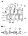
- Fig. 3 is a plan view illustrating a part of the organic electroluminescent device, according to the present invention. For convenience sake, only a part of four columns of anode electrode layer 10, 20, 30 and 40, formed on the substrate 100, are illustrated.
- An Indium Tin Oxide (ITO) layer is preferred for the anode electrode layer, and is exemplified below.
- each column of ITO layer 10, 20, 30 and 40 includes two ITO layers 11, 12 and 21, 22.
- ITO layer 11, 12 and 21, 22 includes luminescent areas 11A, 12A, 21A and 22A with predetermined areas spaced from each other and connecting areas 11B, 12B, 21B and 22B connecting the luminescent areas 11A, 12A, 21A and 22A with a predetermined width.
- ITO layers 11 and 12 included in the column of ITO layer 10 are formed apart by a predetermined width.
- Each luminescent area 11A of ITO layer 11 corresponds spatially to each connecting area 12B of ITO layer 12. Therefore, the column of ITO layer 10 has almost the same width as the width of ITO layer 11 or ITO layer 12.
- the metal line of each ITO layer 21 or 22 included in the column of ITO layer 20 is formed in a stack in the same area as the metal line of each corresponding ITO layer 12 or 31 included in an adjacent column of ITO layer 10 or ITO layer 30, respectively.
- Fig. 3 for convenience sake, only four columns of ITO layer 10, 20, 30 and 40 formed on the substrate 100 are illustrated spaced from each other.
- a wiring part is formed between two columns of ITO layer.
- organic layers and cathode electrode layers are formed in sequence.
- a metal layer is preferred for the cathode electrode layer, and is exemplified so below.
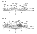
- Figs. 4a - 4f are sectional views along the line B-B of Fig. 3, illustrating the step-by-step manufacturing method of the organic electroluminescent device according to an embodiment of the present invention.
- the ITO layers 12 and 21 corresponding to each other included in two adjacent columns of ITO layer 10 and 20 are exemplified.
- the columns of ITO layer 10 and 20 are formed on the substrate 100 (see Fig. 3 and Fig. 4a).
- a first metal line M12 of a first ITO layer 12 included in a first column of ITO layer 10 and a second metal line M21 of a second ITO layer 21 included in a second column of ITO layer 20 are formed in the same area, which is defined as "a wiring part.”
- the first metal line M12 is formed along a first data line 12B connected to the first ITO layer 12 on the first data line 12B (Fig. 4b). Molybdenum is a preferred material for the first metal line M12. It is preferable to make the width of the first metal line M12 the same as that of the first data line 12B.
- an insulating layer 50 is formed on the first metal line M12, a part of the second ITO layer 21, and the substrate 100 between the first ITO layer 12 and the second ITO layer 21 (Fig. 4c).
- the second data line 21B is formed on the insulating layer 50 (Fig. 4d), and connected to the second ITO layer 21.
- the second metal line M21 is formed on the second data line 21B (Fig. 4e). It is preferable to make the width of the second metal line M21 the same as that of the first metal line M12.
- the first metal line M12 and the second metal line M21 are connected to a pad part formed at the end of the substrate 100.
- an insulating layer 60 is formed on the above elements.
- the insulating layer 60 is not formed on the luminescent areas of each ITO layer which are illustrated as dotted lines in Fig. 3.
Abstract
Description
- The present invention relates to an organic electroluminescent device of the active matrix (AM) and passive matrix (PM) types, and a method for manufacturing the same. Particularly, the present invention relates to an organic electroluminescent device and a method for manufacturing the same, capable of achieving high resolution and big size by decreasing a space between the anode electrodes.
- Organic electroluminescence is a phenomenon wherein excitons are formed in an organic (low molecular or high molecular) material thin film by recombining holes injected through an anode with electrons injected through a cathode, and a light of specific wavelength is generated by energy from thus formed excitons. The basic structure of an organic electroluminescent device using the phenomenon and a method for manufacturing the same will be described hereinafter.
- Fig. 1 is a plan view of an organic electroluminescent device, in accordance with the related art. Fig. 2 is a cross-sectional view of the organic electroluminescent device of Fig. 1, as taken along line A-A.
- The basic structure of an organic electroluminescent device includes a
glass substrate 1, ananode electrode layer 2 formed on the upper side of theglass substrate 1, an organic material layer 3 (hereinafter, referred to as "organic EL layer") formed on theanode electrode layer 2, and acathode electrode layer 4 formed on theorganic EL layer 3. - The
organic EL layer 3 has a structure wherein a hole transport layer, a light emitting layer and an electron transport layer are stacked in order. Eachcathode electrode layer 4 maintains a certain space from adjacentcathode electrode layers 4. Theanode electrode layer 2 acts as an anode electrode, and thecathode electrode layer 4 acts as a cathode electrode. - A
wall 5 separates two adjacentcathode electrode layers 4. Thewall 5 is formed in an area between two adjacentcathode electrode layers 4. Thewall 5 is separated from theanode electrode layer 2 by aninsulating layer 4a. Although organic material and cathode electrode material are deposited on the upper side or top of eachwall 5 during the processes of forming theorganic EL layer 3 andcathode electrode layer 4, neither functions as a component of the device. - The organic electroluminescent device having the above structure is manufactured by the following processes.
- First, a plurality of
anode electrode layers 2 are deposited on aglass substrate 1, and then aninsulating layer 4a is formed on the entire surface area of thesubstrate 1 except predetermined areas (luminescent areas). - Then, a plurality of
walls 5 crossing theanode electrode layers 2 are formed thereon, followed by formingorganic EL layers 3 andcathode electrode layers 4 on the entire structure including thewalls 5. - In the organic electroluminescent device of the related art, illustrated in Fig. 1, predetermined spaces exist between
anode electrode layers 2. In a high resolution display device, in which the number of luminescent areas per unit area is increased, these spaces between theanode electrode layers 2 become a major concern. Since the spacing betweenanode layers 2 is predetermined, a large number of luminescent areas requires an increase in the size of the display device to accommodate the many required spaces between theanode electrodes layers 2, which is counter to the higher resolution goal, i.e. more luminescent areas per unit area. - An object of the present invention is to address one or more of the drawbacks associated with the related art.
- It is an object of the present invention to provide an organic electroluminescent device having a structure which can increase the number of luminescent areas per unit area, without increasing a size of the panel, to resolve the above problem of the related art display.
- The organic electroluminescent device according to the present invention comprises anode electrode layers; cathode electrode layers disposed to intersect (e.g. overlie or underlie) with the anode electrode layers; organic layers formed in each intersecting part where one cathode electrode layer and two anode electrode layers intersect; and a multi-layered wiring part for supplying driving signals to each of a first anode electrode layer of a first intersecting part and a second anode electrode layer of a second intersecting part adjacent to the first anode electrode layer.
- Preferably, the wiring part comprises a first data line connected to the first anode electrode layer; a first metal line formed on the first data line; an insulating layer formed on the first metal line and a part of the second anode electrode layer; a second data line formed on the insulating layer and connected to the second anode electrode layer; and a second metal line formed on the second data line.
- A manufacturing method of the organic electroluminescent device according to the present invention comprises the steps of forming anode electrode layers on a substrate in parallel; forming organic layers on the anode electrode layers; forming cathode electrode layers on the organic layers, wherein each of the cathode electrode layers intersects with two anode electrode layers in an intersecting part; and forming multi-layered wiring parts for supplying driving current independently to a first anode electrode layer of a first intersecting part and a second anode electrode layer of a second intersecting part adjacent to the first anode electrode layer.
- The step of forming the wiring parts comprises the steps of forming a first metal line on a first data line connected to the first anode electrode layer; forming an insulating layer on the first metal line, a part of the second anode electrode layer, and the substrate between the two anode electrode layers; forming a second data line connected to the second anode electrode layer on the insulating layer; and forming a second metal line on the second data line.
- The organic electroluminescent device according to the present invention forms stacked metal lines which can supply driving current (data current) independently to each of two anode electrode layers in a space between two columns of anode electrode layer. Thus, the space between two anode electrode layers can be minimized, and the size of the device can be remarkably minimized.
- These and other objects of the present application will become more readily apparent from the detailed description given hereinafter. However, it should be understood that the detailed description and specific examples, while indicating preferred embodiments of the invention, are given by way of illustration only, since various changes and modifications within the spirit and scope of the invention will become apparent to those skilled in the art from this detailed description.
- The present invention will be more clearly understood from the detailed description in conjunction with the following drawings.
- Fig. 1 is a plan view of an organic electroluminescent device, in accordance with the related art;
- Fig. 2 is a cross-sectional view of the organic electroluminescent device of Fig. 1, as taken along line A-A;
- Fig. 3 is a plan view illustrating a part of the organic electroluminescent device according to the present invention; and
- Figs. 4a-4f are sectional views along the line B-B, illustrating a step-by-step manufacturing method of the organic electroluminescent device according to the present invention.
- Hereinafter, a preferred embodiment of the organic electroluminescent device according to the present invention will be explained in more detail with reference to the accompanying drawings.
- Fig. 3 is a plan view illustrating a part of the organic electroluminescent device, according to the present invention. For convenience sake, only a part of four columns of
anode electrode layer substrate 100, are illustrated. An Indium Tin Oxide (ITO) layer is preferred for the anode electrode layer, and is exemplified below. - As described above, each column of
ITO layer ITO layers ITO layer ITO layer luminescent areas areas luminescent areas - Two
ITO layers ITO layer 10 are formed apart by a predetermined width. Eachluminescent area 11A ofITO layer 11 corresponds spatially to each connectingarea 12B ofITO layer 12. Therefore, the column ofITO layer 10 has almost the same width as the width ofITO layer 11 orITO layer 12. - The metal line of each
ITO layer 21 or 22 included in the column ofITO layer 20 is formed in a stack in the same area as the metal line of eachcorresponding ITO layer 12 or 31 included in an adjacent column ofITO layer 10 orITO layer 30, respectively. - Hereinafter, a preferred embodiment of the manufacturing method of the organic electroluminescent device according to an embodiment of the present invention will be explained in more detail with reference to Fig. 3 and Figs. 4a - 4f.
- In Fig. 3, for convenience sake, only four columns of
ITO layer substrate 100 are illustrated spaced from each other. Through the steps illustrated in Fig. 4a to Fig. 4f, a wiring part is formed between two columns of ITO layer. Then, organic layers and cathode electrode layers are formed in sequence. A metal layer is preferred for the cathode electrode layer, and is exemplified so below. - Figs. 4a - 4f are sectional views along the line B-B of Fig. 3, illustrating the step-by-step manufacturing method of the organic electroluminescent device according to an embodiment of the present invention. In Figs. 4a - 4f, for convenience sake, the
ITO layers ITO layer - As explained above, the columns of
ITO layer - Then, a first metal line M12 of a
first ITO layer 12 included in a first column ofITO layer 10 and a second metal line M21 of asecond ITO layer 21 included in a second column ofITO layer 20 are formed in the same area, which is defined as "a wiring part." - First, the first metal line M12 is formed along a
first data line 12B connected to thefirst ITO layer 12 on thefirst data line 12B (Fig. 4b). Molybdenum is a preferred material for the first metal line M12. It is preferable to make the width of the first metal line M12 the same as that of thefirst data line 12B. - Then, an insulating
layer 50 is formed on the first metal line M12, a part of thesecond ITO layer 21, and thesubstrate 100 between thefirst ITO layer 12 and the second ITO layer 21 (Fig. 4c). - Then, the
second data line 21B is formed on the insulating layer 50 (Fig. 4d), and connected to thesecond ITO layer 21. - After the
second data line 21B is formed, the second metal line M21 is formed on thesecond data line 21B (Fig. 4e). It is preferable to make the width of the second metal line M21 the same as that of the first metal line M12. The first metal line M12 and the second metal line M21 are connected to a pad part formed at the end of thesubstrate 100. - After the second metal line M21 is formed, an insulating
layer 60 is formed on the above elements. The insulatinglayer 60 is not formed on the luminescent areas of each ITO layer which are illustrated as dotted lines in Fig. 3. - Walls to separate metal layers on the insulating layers are formed across the columns of
ITO layer organic layers 3 and metal layers (e.g. cathode electrode layers 4) are formed on the above elements in sequence, as illustrated in Fig. 4f, to complete the manufacturing method of the organic electroluminescent device according to the present invention. - From the preferred embodiment for the present invention, it is noted that modifications and variations can be made by a person skilled in the art in light of the above teachings. For example, although the
anode electrode layer 2 has been illustrated as being on thesubstrate 100 with the cathode electrode layer being above, it would be possible to reverse this orientation such at the cathode layer is first applied to the substrate. Such an arrangement is intended to be covered by the overlying and underlying language used herein. - Also, although the invention has been described in a situation where one
cathode electrode layer 4 underlies or overlies two anode electrode layers 2. Of course, three or moreanode electrode layers 2 could overlap with onecathode electrode layer 4, such that three or more sets of data lines and metal lines would be present in the multi-layered structure of Fig. 4d. In such an instance, an additional data line (a mirror-image of thedata line 21B in Fig. 4d) would be added to the multi-layered structure to electrically communicate with a thirdanode electrode layer 2 disposed on the left side of the multi-layered structure, as viewed in the perspective of Fig. 4d. - Therefore, it should be understood that changes may be made for a particular embodiment of the present invention within the scope and the spirit of the present invention outlined by the appended claims.
Claims (20)
- An organic electroluminescent device comprising:anode electrode layers;cathode electrode layers disposed to overlie or underlie the anode electrode layers;organic layers formed in parts where one cathode electrode layer overlies or underlies two anode electrode layers; anda multi-layered structure including two data lines, a first data line for supplying driving signals to a first anode electrode layer of said two anode electrode layers and a second data line for supplying driving signals to a second anode electrode layer of said two anode electrode layers, wherein said first and second data lines reside on different layers of said multi-layer structure.
- The organic electroluminescent device of claim 1, wherein said first data line overlies or underlies said second data line in a cross section of said multi-layered structure.
- The organic electroluminescent device of claim 1, wherein said first and second anode electrode layers reside adjacent to each other on said organic electroluminescent device.
- The organic electroluminescent device of claim 3, further comprising:an insulating layer residing between said first and second anode electrode layers.
- The organic electroluminescent device of claim 4, further comprising:a first metal line overlying said first data line, wherein said insulating layer overlies said first metal line.
- The organic electroluminescent device of claim 5, wherein a width of said first data line is substantially the same as a width of said first metal line.
- The organic electroluminescent device of claim 5, wherein said second data line overlies said insulating layer.
- The organic electroluminescent device of claim 5, wherein said insulating layer also partially overlies said second anode electrode layer.
- The organic electroluminescent device of claim 8, wherein said second data line overlies said insulating layer.
- The organic electroluminescent device of claim 9, further comprising:a second metal line overlying said second data line.
- The organic electroluminescent device of claim 10, wherein a width of said second metal line is substantially the same as a width of said first metal line.
- An organic electroluminescent device comprising:anode electrode layers;cathode electrode layers disposed to overlie or underlie the anode electrode layers;organic layers formed in parts where a cathode electrode layer overlies or underlies at least two anode electrode layers; anda multi-layered structure including at least two data lines, a first data line for supplying driving signals to a first anode electrode layer of said at least two anode electrode layers and a second data line for supplying driving signals to a second anode electrode layer of said at least two anode electrode layers, wherein said first and second data lines reside on different layers of said multi-layered structure.
- The organic electroluminescent device of claim 12, wherein said first and second anode electrode layers reside adjacent to each other on said organic electroluminescent device, and further comprising:an insulating layer residing between said first and second anode electrode layers.
- The organic electroluminescent device of claim 13, further comprising:a first metal line overlying said first data line, wherein said insulating layer overlies said first metal line.
- The organic electroluminescent device of claim 14, wherein said second data line overlies said insulating layer, and further comprising:a second metal line overlying said second data line.
- The organic electroluminescent device of claim 15, wherein a width of said second metal line is substantially the same as a width of said first metal line.
- A method of manufacturing an organic electroluminescent device comprising the steps of:forming anode electrode layers;forming organic layers on the anode electrode layers;forming cathode electrode layers on the organic layers, wherein each of the cathode electrode layers overlies or underlies at least two anode electrode layers; andforming a multi-layered structure including at least two data lines, a first data line for supplying driving signals to a first anode electrode layer of the at least two anode electrode layers and a second data line for supplying driving signals to a second anode electrode layer of the at least two anode electrode layers, wherein said first andsecond data lines reside on different layers of the multi-layer structure.
- The method of claim 17, further comprising:forming an insulating layer residing between said first and second anode electrode layers.
- The method of claim 18, further comprising:forming a first metal line overlying the first data line, wherein the insulating layer overlies the first metal line.
- The method of claim 19, further comprising:forming the second data line to overlie the insulating layer; andforming a second metal line to overlie the second data line.
Applications Claiming Priority (1)
| Application Number | Priority Date | Filing Date | Title |
|---|---|---|---|
| KR1020040112144A KR100687216B1 (en) | 2004-12-24 | 2004-12-24 | Organic electroluminescent device and method for manufacturing the same |
Publications (2)
| Publication Number | Publication Date |
|---|---|
| EP1684353A2 true EP1684353A2 (en) | 2006-07-26 |
| EP1684353A3 EP1684353A3 (en) | 2011-04-27 |
Family
ID=36072137
Family Applications (1)
| Application Number | Title | Priority Date | Filing Date |
|---|---|---|---|
| EP05027743A Withdrawn EP1684353A3 (en) | 2004-12-24 | 2005-12-19 | Organic electroluminescent device and method for manufacturing the same |
Country Status (5)
| Country | Link |
|---|---|
| US (1) | US7550920B2 (en) |
| EP (1) | EP1684353A3 (en) |
| JP (1) | JP2006185915A (en) |
| KR (1) | KR100687216B1 (en) |
| CN (1) | CN100508205C (en) |
Cited By (1)
| Publication number | Priority date | Publication date | Assignee | Title |
|---|---|---|---|---|
| EP2109164A1 (en) * | 2007-01-24 | 2009-10-14 | Nippon Seiki Co., Ltd. | Organic el display |
Families Citing this family (2)
| Publication number | Priority date | Publication date | Assignee | Title |
|---|---|---|---|---|
| CN102110707B (en) * | 2010-11-23 | 2013-07-03 | 友达光电股份有限公司 | Light emitting device and manufacturing method thereof |
| CN109860416B (en) * | 2019-01-09 | 2022-03-25 | 昆山工研院新型平板显示技术中心有限公司 | Pixel structure and OLED display panel with same |
Citations (5)
| Publication number | Priority date | Publication date | Assignee | Title |
|---|---|---|---|---|
| EP0888035A1 (en) * | 1996-03-12 | 1998-12-30 | Idemitsu Kosan Company Limited | Organic electroluminescent element and organic electroluminescent display |
| JP2000029432A (en) * | 1998-07-08 | 2000-01-28 | Tdk Corp | Organic el display device |
| JP2001217081A (en) * | 2000-02-02 | 2001-08-10 | Sharp Corp | Organic light emitting display device |
| JP2001313182A (en) * | 2000-05-01 | 2001-11-09 | Toyota Motor Corp | Organic el display device |
| EP1286395A2 (en) * | 2001-08-21 | 2003-02-26 | Lg Electronics Inc. | Organic electroluminescence device |
Family Cites Families (3)
| Publication number | Priority date | Publication date | Assignee | Title |
|---|---|---|---|---|
| KR100906964B1 (en) * | 2002-09-25 | 2009-07-08 | 삼성전자주식회사 | Element for driving organic light emitting device and display panel for organic light emitting device with the same |
| KR100656510B1 (en) * | 2003-07-01 | 2006-12-13 | 엘지전자 주식회사 | Organic electroluminescent device and method of manufacturing the same |
| KR100621865B1 (en) * | 2003-12-29 | 2006-09-13 | 엘지.필립스 엘시디 주식회사 | Organic Electro-luminescence Display Device And Fabricating Method Thereof |
-
2004
- 2004-12-24 KR KR1020040112144A patent/KR100687216B1/en not_active IP Right Cessation
-
2005
- 2005-12-19 EP EP05027743A patent/EP1684353A3/en not_active Withdrawn
- 2005-12-20 JP JP2005366723A patent/JP2006185915A/en active Pending
- 2005-12-22 US US11/313,998 patent/US7550920B2/en not_active Expired - Fee Related
- 2005-12-26 CN CNB2005101362833A patent/CN100508205C/en not_active Expired - Fee Related
Patent Citations (5)
| Publication number | Priority date | Publication date | Assignee | Title |
|---|---|---|---|---|
| EP0888035A1 (en) * | 1996-03-12 | 1998-12-30 | Idemitsu Kosan Company Limited | Organic electroluminescent element and organic electroluminescent display |
| JP2000029432A (en) * | 1998-07-08 | 2000-01-28 | Tdk Corp | Organic el display device |
| JP2001217081A (en) * | 2000-02-02 | 2001-08-10 | Sharp Corp | Organic light emitting display device |
| JP2001313182A (en) * | 2000-05-01 | 2001-11-09 | Toyota Motor Corp | Organic el display device |
| EP1286395A2 (en) * | 2001-08-21 | 2003-02-26 | Lg Electronics Inc. | Organic electroluminescence device |
Cited By (2)
| Publication number | Priority date | Publication date | Assignee | Title |
|---|---|---|---|---|
| EP2109164A1 (en) * | 2007-01-24 | 2009-10-14 | Nippon Seiki Co., Ltd. | Organic el display |
| EP2109164A4 (en) * | 2007-01-24 | 2011-06-01 | Nippon Seiki Co Ltd | Organic el display |
Also Published As
| Publication number | Publication date |
|---|---|
| JP2006185915A (en) | 2006-07-13 |
| CN100508205C (en) | 2009-07-01 |
| US7550920B2 (en) | 2009-06-23 |
| KR100687216B1 (en) | 2007-02-27 |
| KR20060073754A (en) | 2006-06-29 |
| EP1684353A3 (en) | 2011-04-27 |
| US20060138949A1 (en) | 2006-06-29 |
| CN1819257A (en) | 2006-08-16 |
Similar Documents
| Publication | Publication Date | Title |
|---|---|---|
| US7368868B2 (en) | Active matrix organic EL display panel | |
| KR100267964B1 (en) | Organic electroluminescent display panel and method for fabricating the same | |
| JP4206388B2 (en) | Flat panel display device | |
| KR102578834B1 (en) | Organic Light Emitting Display Device | |
| US6930448B2 (en) | Organic electroluminescence display panel and fabrication method thereof | |
| EP1914816A2 (en) | Light emitting panel and light source apparatus having the same | |
| JP7024937B2 (en) | Array board, display panel and display device | |
| US7122956B2 (en) | OLED display and method of manufacturing such display | |
| CN110402496B (en) | Display substrate, display device, and method of manufacturing display substrate | |
| US6882103B2 (en) | Panel of organic electroluminescence device and method for manufacturing the same | |
| US11016624B2 (en) | Touch display panel and manufacturing method thereof, display device | |
| US20110163980A1 (en) | Organic light emitting diode display and method of manufacturing the same | |
| US7221094B2 (en) | Electroluminescent device and method of manufacturing the same | |
| US6717357B2 (en) | Organic electroluminescent display panel | |
| US7550920B2 (en) | Organic electroluminescent device and method for manufacturing the same | |
| JPH11224778A (en) | Electroluminescence light source | |
| US20020158576A1 (en) | Light-emitting device and light-emitting device manufacturing method | |
| JP6587952B2 (en) | Organic EL display device | |
| JP4639662B2 (en) | Electro-optical device and electronic apparatus | |
| KR20070065588A (en) | Organic light emitting diode | |
| JP4392113B2 (en) | Organic electroluminescence display panel and organic electroluminescence display panel manufacturing method | |
| US7687889B2 (en) | Organic electroluminescent display device having electrical communication between conducting layer and cathode layer | |
| CN210073855U (en) | Array substrate, display panel and display device | |
| WO2011055621A1 (en) | Organic el panel | |
| WO2017029889A1 (en) | Organic el panel, illuminating device, and method for manufacturing organic el panel |
Legal Events
| Date | Code | Title | Description |
|---|---|---|---|
| PUAI | Public reference made under article 153(3) epc to a published international application that has entered the european phase |
Free format text: ORIGINAL CODE: 0009012 |
|
| 17P | Request for examination filed |
Effective date: 20051219 |
|
| AK | Designated contracting states |
Kind code of ref document: A2 Designated state(s): AT BE BG CH CY CZ DE DK EE ES FI FR GB GR HU IE IS IT LI LT LU LV MC NL PL PT RO SE SI SK TR |
|
| AX | Request for extension of the european patent |
Extension state: AL BA HR MK YU |
|
| PUAL | Search report despatched |
Free format text: ORIGINAL CODE: 0009013 |
|
| AK | Designated contracting states |
Kind code of ref document: A3 Designated state(s): AT BE BG CH CY CZ DE DK EE ES FI FR GB GR HU IE IS IT LI LT LU LV MC NL PL PT RO SE SI SK TR |
|
| AX | Request for extension of the european patent |
Extension state: AL BA HR MK YU |
|
| STAA | Information on the status of an ep patent application or granted ep patent |
Free format text: STATUS: THE APPLICATION HAS BEEN WITHDRAWN |
|
| 18W | Application withdrawn |
Effective date: 20110629 |