EP1684298A2 - Electronic equipment comprising shock sensitive memory device - Google Patents
Electronic equipment comprising shock sensitive memory device Download PDFInfo
- Publication number
- EP1684298A2 EP1684298A2 EP06250255A EP06250255A EP1684298A2 EP 1684298 A2 EP1684298 A2 EP 1684298A2 EP 06250255 A EP06250255 A EP 06250255A EP 06250255 A EP06250255 A EP 06250255A EP 1684298 A2 EP1684298 A2 EP 1684298A2
- Authority
- EP
- European Patent Office
- Prior art keywords
- electronic equipment
- circuit board
- holding member
- memory device
- hdd
- Prior art date
- Legal status (The legal status is an assumption and is not a legal conclusion. Google has not performed a legal analysis and makes no representation as to the accuracy of the status listed.)
- Withdrawn
Links
Images



Classifications
-
- H—ELECTRICITY
- H05—ELECTRIC TECHNIQUES NOT OTHERWISE PROVIDED FOR
- H05K—PRINTED CIRCUITS; CASINGS OR CONSTRUCTIONAL DETAILS OF ELECTRIC APPARATUS; MANUFACTURE OF ASSEMBLAGES OF ELECTRICAL COMPONENTS
- H05K3/00—Apparatus or processes for manufacturing printed circuits
- H05K3/30—Assembling printed circuits with electric components, e.g. with resistors
- H05K3/301—Assembling printed circuits with electric components, e.g. with resistors by means of a mounting structure
-
- G—PHYSICS
- G11—INFORMATION STORAGE
- G11B—INFORMATION STORAGE BASED ON RELATIVE MOVEMENT BETWEEN RECORD CARRIER AND TRANSDUCER
- G11B25/00—Apparatus characterised by the shape of record carrier employed but not specific to the method of recording or reproducing, e.g. dictating apparatus; Combinations of such apparatus
- G11B25/04—Apparatus characterised by the shape of record carrier employed but not specific to the method of recording or reproducing, e.g. dictating apparatus; Combinations of such apparatus using flat record carriers, e.g. disc, card
- G11B25/043—Apparatus characterised by the shape of record carrier employed but not specific to the method of recording or reproducing, e.g. dictating apparatus; Combinations of such apparatus using flat record carriers, e.g. disc, card using rotating discs
-
- G—PHYSICS
- G11—INFORMATION STORAGE
- G11B—INFORMATION STORAGE BASED ON RELATIVE MOVEMENT BETWEEN RECORD CARRIER AND TRANSDUCER
- G11B33/00—Constructional parts, details or accessories not provided for in the other groups of this subclass
- G11B33/02—Cabinets; Cases; Stands; Disposition of apparatus therein or thereon
- G11B33/08—Insulation or absorption of undesired vibrations or sounds
-
- H—ELECTRICITY
- H05—ELECTRIC TECHNIQUES NOT OTHERWISE PROVIDED FOR
- H05K—PRINTED CIRCUITS; CASINGS OR CONSTRUCTIONAL DETAILS OF ELECTRIC APPARATUS; MANUFACTURE OF ASSEMBLAGES OF ELECTRICAL COMPONENTS
- H05K1/00—Printed circuits
- H05K1/02—Details
- H05K1/0271—Arrangements for reducing stress or warp in rigid printed circuit boards, e.g. caused by loads, vibrations or differences in thermal expansion
-
- H—ELECTRICITY
- H05—ELECTRIC TECHNIQUES NOT OTHERWISE PROVIDED FOR
- H05K—PRINTED CIRCUITS; CASINGS OR CONSTRUCTIONAL DETAILS OF ELECTRIC APPARATUS; MANUFACTURE OF ASSEMBLAGES OF ELECTRICAL COMPONENTS
- H05K1/00—Printed circuits
- H05K1/02—Details
- H05K1/14—Structural association of two or more printed circuits
- H05K1/141—One or more single auxiliary printed circuits mounted on a main printed circuit, e.g. modules, adapters
-
- H—ELECTRICITY
- H05—ELECTRIC TECHNIQUES NOT OTHERWISE PROVIDED FOR
- H05K—PRINTED CIRCUITS; CASINGS OR CONSTRUCTIONAL DETAILS OF ELECTRIC APPARATUS; MANUFACTURE OF ASSEMBLAGES OF ELECTRICAL COMPONENTS
- H05K1/00—Printed circuits
- H05K1/02—Details
- H05K1/14—Structural association of two or more printed circuits
- H05K1/147—Structural association of two or more printed circuits at least one of the printed circuits being bent or folded, e.g. by using a flexible printed circuit
-
- H—ELECTRICITY
- H05—ELECTRIC TECHNIQUES NOT OTHERWISE PROVIDED FOR
- H05K—PRINTED CIRCUITS; CASINGS OR CONSTRUCTIONAL DETAILS OF ELECTRIC APPARATUS; MANUFACTURE OF ASSEMBLAGES OF ELECTRICAL COMPONENTS
- H05K1/00—Printed circuits
- H05K1/18—Printed circuits structurally associated with non-printed electric components
- H05K1/182—Printed circuits structurally associated with non-printed electric components associated with components mounted in printed circuit boards [PCB], e.g. insert-mounted components [IMC]
-
- H—ELECTRICITY
- H05—ELECTRIC TECHNIQUES NOT OTHERWISE PROVIDED FOR
- H05K—PRINTED CIRCUITS; CASINGS OR CONSTRUCTIONAL DETAILS OF ELECTRIC APPARATUS; MANUFACTURE OF ASSEMBLAGES OF ELECTRICAL COMPONENTS
- H05K2201/00—Indexing scheme relating to printed circuits covered by H05K1/00
- H05K2201/01—Dielectrics
- H05K2201/0104—Properties and characteristics in general
- H05K2201/0133—Elastomeric or compliant polymer
-
- H—ELECTRICITY
- H05—ELECTRIC TECHNIQUES NOT OTHERWISE PROVIDED FOR
- H05K—PRINTED CIRCUITS; CASINGS OR CONSTRUCTIONAL DETAILS OF ELECTRIC APPARATUS; MANUFACTURE OF ASSEMBLAGES OF ELECTRICAL COMPONENTS
- H05K2201/00—Indexing scheme relating to printed circuits covered by H05K1/00
- H05K2201/10—Details of components or other objects attached to or integrated in a printed circuit board
- H05K2201/10007—Types of components
- H05K2201/10159—Memory
-
- H—ELECTRICITY
- H05—ELECTRIC TECHNIQUES NOT OTHERWISE PROVIDED FOR
- H05K—PRINTED CIRCUITS; CASINGS OR CONSTRUCTIONAL DETAILS OF ELECTRIC APPARATUS; MANUFACTURE OF ASSEMBLAGES OF ELECTRICAL COMPONENTS
- H05K2201/00—Indexing scheme relating to printed circuits covered by H05K1/00
- H05K2201/10—Details of components or other objects attached to or integrated in a printed circuit board
- H05K2201/10431—Details of mounted components
- H05K2201/10606—Permanent holder for component or auxiliary printed circuits mounted on a printed circuit board [PCB]
Definitions
- the present invention relates to a compact electronic equipment such as a digital camera, a digital audio equipment, or the like equipped with a mass storage vulnerable to a shock.
- HDD high-capacity hard disk drive
- an HDD packed with a shock absorber or a vibration absorber is disposed in the vicinity of a circuit board including a controller circuit of an electronic equipment through an insulator, so that it causes a problem that the dimension of the electronic equipment becomes thick.
- the present invention is made in view of the aforementioned problems and has an object to provide an electronic equipment satisfying both compactness and resistance to a shock and a shake in spite of being equipped with a memory device such as an HDD vulnerable to a shock.
- an electronic equipment including a memory device that stores data thereon, a circuit board that has an opening portion and a control circuit for controlling the electronic equipment, and a holding member that holds the memory device at the opening portion.
- the memory device is vulnerable to a shock.
- the opening portion is formed by cutting out at least one side of the circuit board.
- At least one side of the holding member makes contact with a casing.
- the electronic equipment further comprises a flexible printed circuit board that electrically connects the memory device to the circuit board.
- the holding member is made of an impact-absorbing material.
- Fig. 1 is a cross sectional view of an electronic equipment according to a first embodiment of the present invention sectioned along an A-A line in Fig. 2.
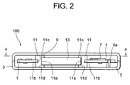
- Fig. 2 is a cross sectional view of the electronic equipment sectioned along a B-B line in Fig. 1.
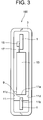
- Fig. 3 is a cross sectional view of the electronic equipment sectioned along a C-C line in Fig. 1.
- Fig. 4 is a cross sectional view of an electronic equipment according to a variation of the present invention sectioned along an A-A line in Fig. 5.
- Fig. 5 is a cross sectional view of the electronic equipment sectioned along a B-B line in Fig. 4.
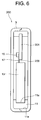
- Fig. 6 is a cross sectional view of the electronic equipment sectioned along a C-C line in Fig. 4.
- reference number 1 denotes a circuit board that is fixed to a casing 3, with being separated from inner walls thereof, through holder portions 5 disposed at four corners of the casing 3 of an electronic equipment 100.
- a fixing means such as a screw 5a or the like is used.
- the fixing means is not limited to the screw 5a and a clip or the like may be used.
- Each of electronic parts 7 for controlling the electronic equipment 100 is mounted and wired on the circuit board 1.
- An opening portion 9 having a square shape is provided at the center of the circuit board 1 and a hard disk drive 13 (hereinafter abbreviated as an "HDD") is held in the space of the casing 3 through a holding member 11.
- HDD hard disk drive 13
- the holding member 11 is formed approximately into a loop having a square shape with a cutout area where a flexible printed circuit board 17 (hereinafter abbreviated as an "FPC") for electrically connecting a connector 15 on the circuit board 1 to the HDD 13 is disposed. Since the FPC 17 connects the HDD 13 to the connector 15 with an allowance so that the FPC 17 may be deformed, even if the HDD 13 is displaced due to a shock or a shake, the electrical connection between the HDD 13 and the connector 15 can be secured.
- FPC flexible printed circuit board 17
- the cross sectional shape of the holding member 11 along the B-B line is a rectangle.
- a groove 11a almost all the way around for holding the HDD 13 by fitting therein.
- the HDD 13 is fitted almost all the way around to be held on the outer circumference thereof by the holding member 11.
- a groove 11b almost all the way around in which edges of the opening portion 9 of the circuit board 1 are fitted to hold the holding member 11. Accordingly, it becomes possible to hold the HDD 13 at the opening portion 9 of the circuit board 1 through the holding member 11 without touching inner wall of the casing 3.
- the HDD 13 may be held such that both of the upper surface 11c (upper side in Fig. 2) and the lower surface 11d (lower side in Fig. 2) of the holding member 11 are separated from the inner wall of the casing 3 or such that at least one surface of the upper surface 11c and the lower surface 11d of the holding member 11 makes contact with the inner wall of the casing 3.
- the electronic equipment equipped with a memory device which is vulnerable to a shock and a shake is constructed.
- the holding member 11 is made of an elastic body (a gel-type material such as rubber, urethane resin, silicone resin, or the like) to absorb a shock and a shake from outside of the casing 3 in order to protect the HDD 13 from a malfunction or a breakdown. Moreover, since the HDD 13 is held at the opening portion 9 of the circuit board 1 through the holding member 11, the whole thickness of the electronic equipment 100 including the circuit board 1 and the HDD 13 can be thinner than that of a conventional construction that the circuit board 1 is disposed in the vicinity of one side of the HDD 13.
- a gel-type material such as rubber, urethane resin, silicone resin, or the like
- the variation is different from the first embodiment in that the opening portion is formed by cutting out at least one side of the circuit board, so that it is explained with attaching the same reference numbers to the similar constructions to the first embodiment.
- reference number 201 denotes a circuit board that is fixed to a casing 3, with being separated from inner walls thereof, through holder portions 5 disposed at four corners of the casing 3 of an electronic equipment 200.
- a fixing means such as a screw 5a or the like is used.
- the fixing means is not limited to the screw 5a and a clip or the like may be used.
- Each of electronic parts 7 for controlling the electronic equipment 200 is mounted and wired on the circuit board 201.
- An opening portion 209 having a square shape is provided at the lower side portion (lower side in Fig. 4) of the circuit board 201 and a hard disk drive 13 (hereinafter abbreviated as an "HDD") is held in the space of the casing 3 through a holding member 11.
- HDD hard disk drive 13
- the holding member 11 is formed approximately into a loop having a square shape with a cutout area where a flexible printed circuit board 17 (hereinafter abbreviated as an "FPC") for electrically connecting a connector 15 on the circuit board 201 to the HDD 13 is disposed. Since the FPC 17 connects the HDD 13 to the connector 15 with an allowance so that the FPC 17 may be deformed, even if the HDD 13 is displaced due to a shock or a shake, the electrical connection between the HDD 13 and the connector 15 can be secured.
- FPC flexible printed circuit board 17
- the cross sectional shape of the holding member 11 along the B-B line is substantially rectangular.
- a groove 11a almost all the way around for holding the HDD 13 by fitting therein.
- the HDD 13 is fitted almost all the way around to be held on the outer circumference by the holding member 11.
- a groove 11b in which edges of the opening portion 209 of the circuit board 201 are fitted to hold the holding member 11 on three sides except one side 11e where the holing member 11 makes contact with the inner wall of the casing 3.
- the side wall portion 11e of the outer circumference of the holding member 11 makes contact with the inner wall of the casing 3.
- the opening portion 209 formed on the circuit board 201 may be formed on any other side of the circuit board 201.
- the cutout length L (see Fig. 4) may be suitably changed in accordance with the corresponding side length of the HDD 13.
- the HDD 13 may be held such that both of the upper surface 11c (upper side in Fig. 5) and the lower surface 11d (lower side in Fig. 5) of the holding member 11 are separated from the inner wall of the casing 3 or such that at least one surface of the upper surface 11c and the lower surface 11d of the holding member 11 makes contact with the inner wall of the casing 3.
- the holding member 11 is made of an elastic body (a gel-type material such as rubber, urethane resin, silicone resin, or the like) to absorb a shock and a shake from outside of the casing 3 in order to protect the HDD 13 from a malfunction or a breakdown.
- a gel-type material such as rubber, urethane resin, silicone resin, or the like
- the whole thickness of the electronic equipment 200 including the circuit board 201 and the HDD 13 can be thinner than that of a conventional construction that the circuit board 201 is disposed in the vicinity of one side of the HDD 13.
- the memory device to be protected is an HDD 13
- the present invention can be applied to hold a memory device vulnerable to a shock and a shake, such as an optical disk drive, and the like.
- An electronic equipment equipped with the memory device according to the first embodiment or the variation of the present invention makes it possible to construct a portion or the whole of an equipment such as a digital camera, a digital video camera, a portable digital audio equipment, a portable MP3 equipment, a PDA equipment, a portable measuring instrument, and the like.
Landscapes
- Engineering & Computer Science (AREA)
- Manufacturing & Machinery (AREA)
- Microelectronics & Electronic Packaging (AREA)
- Mounting Of Printed Circuit Boards And The Like (AREA)
- Casings For Electric Apparatus (AREA)
Abstract
Description
- The disclosure of the following priority application is herein incorporated by reference:
Japanese Patent Application No. 2005-015969 filed on January 24, 2005. - The present invention relates to a compact electronic equipment such as a digital camera, a digital audio equipment, or the like equipped with a mass storage vulnerable to a shock.
- Recently, a compact electronic equipment such as a digital camera, a digital audio equipment, or the like equipped with a high-capacity hard disk drive (hereinafter called an "HDD") as a mass storage has been put on the market. Since a high-capacity hard disk drive is vulnerable to a shock and a shake, upon being installed in an electronic equipment the HDD is protected from a shock and a shake by packing it up with a shock absorber or a vibration absorber (for example, see Japanese Patent Application Laid-Open No. 2003-242764).
- Nowadays, a digital camera or a portable audio equipment equipped with an HDD is being expected to become further compact. However, in the embodiment of Japanese Patent Application Laid-Open No. 2003-242764, an HDD packed with a shock absorber or a vibration absorber is disposed in the vicinity of a circuit board including a controller circuit of an electronic equipment through an insulator, so that it causes a problem that the dimension of the electronic equipment becomes thick.
- The present invention is made in view of the aforementioned problems and has an object to provide an electronic equipment satisfying both compactness and resistance to a shock and a shake in spite of being equipped with a memory device such as an HDD vulnerable to a shock.
- According to one aspect of the present invention, there is provided an electronic equipment including a memory device that stores data thereon, a circuit board that has an opening portion and a control circuit for controlling the electronic equipment, and a holding member that holds the memory device at the opening portion.
- In the aspect of the present invention, it is characterized in that the memory device is vulnerable to a shock.
- In the aspect of the present invention, it is preferable that the opening portion is formed by cutting out at least one side of the circuit board.
- In the aspect of the present invention, it is preferable that at least one side of the holding member makes contact with a casing.
- In the aspect of the present invention, it is preferable that the electronic equipment further comprises a flexible printed circuit board that electrically connects the memory device to the circuit board.
- In the aspect of the present invention, it is preferable that the holding member is made of an impact-absorbing material.
- Other features and advantages according to the invention will be readily understood from the detailed description of the preferred embodiment in conjunction with the accompanying drawings.
-
- Fig. 1 is a cross sectional view of an electronic equipment according to a first embodiment of the present invention sectioned along an A-A line in Fig. 2.
- Fig. 2 is a cross sectional view of the electronic equipment sectioned along a B-B line in Fig. 1.
- Fig. 3 is a cross sectional view of the electronic equipment sectioned along a C-C line in Fig. 1.
- Fig. 4 is a cross sectional view of an electronic equipment according to a variation of the present invention sectioned along an A-A line in Fig. 5.
- Fig. 5 is a cross sectional view of the electronic equipment sectioned along a B-B line in Fig. 4.
- Fig. 6 is a cross sectional view of the electronic equipment sectioned along a C-C line in Fig. 4.
- Embodiments according to the present invention is explained below with reference to accompanying drawings.
- Fig. 1 is a cross sectional view of an electronic equipment according to a first embodiment of the present invention sectioned along an A-A line in Fig. 2. Fig. 2 is a cross sectional view of the electronic equipment sectioned along a B-B line in Fig. 1. Fig. 3 is a cross sectional view of the electronic equipment sectioned along a C-C line in Fig. 1. Fig. 4 is a cross sectional view of an electronic equipment according to a variation of the present invention sectioned along an A-A line in Fig. 5. Fig. 5 is a cross sectional view of the electronic equipment sectioned along a B-B line in Fig. 4. Fig. 6 is a cross sectional view of the electronic equipment sectioned along a C-C line in Fig. 4.
- In Figs. 1 to 3,
reference number 1 denotes a circuit board that is fixed to acasing 3, with being separated from inner walls thereof, throughholder portions 5 disposed at four corners of thecasing 3 of anelectronic equipment 100. In order to fix thecircuit board 1 to theholder portions 5, a fixing means such as ascrew 5a or the like is used. The fixing means is not limited to thescrew 5a and a clip or the like may be used. Each ofelectronic parts 7 for controlling theelectronic equipment 100 is mounted and wired on thecircuit board 1. Anopening portion 9 having a square shape is provided at the center of thecircuit board 1 and a hard disk drive 13 (hereinafter abbreviated as an "HDD") is held in the space of thecasing 3 through aholding member 11. - The
holding member 11 is formed approximately into a loop having a square shape with a cutout area where a flexible printed circuit board 17 (hereinafter abbreviated as an "FPC") for electrically connecting aconnector 15 on thecircuit board 1 to theHDD 13 is disposed. Since the FPC 17 connects theHDD 13 to theconnector 15 with an allowance so that the FPC 17 may be deformed, even if theHDD 13 is displaced due to a shock or a shake, the electrical connection between theHDD 13 and theconnector 15 can be secured. - As shown in Fig. 2, the cross sectional shape of the
holding member 11 along the B-B line is a rectangle. In an inner circumference of theholding member 11, there is formed agroove 11a almost all the way around for holding theHDD 13 by fitting therein. In thegroove 11a, theHDD 13 is fitted almost all the way around to be held on the outer circumference thereof by theholding member 11. In an outer circumference of theholding member 11, there is formed agroove 11b almost all the way around in which edges of theopening portion 9 of thecircuit board 1 are fitted to hold theholding member 11. Accordingly, it becomes possible to hold theHDD 13 at theopening portion 9 of thecircuit board 1 through theholding member 11 without touching inner wall of thecasing 3. - Incidentally, in Figs. 2 and 3, the
HDD 13 may be held such that both of theupper surface 11c (upper side in Fig. 2) and thelower surface 11d (lower side in Fig. 2) of theholding member 11 are separated from the inner wall of thecasing 3 or such that at least one surface of theupper surface 11c and thelower surface 11d of theholding member 11 makes contact with the inner wall of thecasing 3. In this manner, the electronic equipment equipped with a memory device which is vulnerable to a shock and a shake is constructed. - In the first embodiment of the present invention, the
holding member 11 is made of an elastic body (a gel-type material such as rubber, urethane resin, silicone resin, or the like) to absorb a shock and a shake from outside of thecasing 3 in order to protect theHDD 13 from a malfunction or a breakdown. Moreover, since theHDD 13 is held at theopening portion 9 of thecircuit board 1 through theholding member 11, the whole thickness of theelectronic equipment 100 including thecircuit board 1 and theHDD 13 can be thinner than that of a conventional construction that thecircuit board 1 is disposed in the vicinity of one side of theHDD 13. - Then, a variation of the present invention is explained with reference to Figs. 4 through 6.
- The variation is different from the first embodiment in that the opening portion is formed by cutting out at least one side of the circuit board, so that it is explained with attaching the same reference numbers to the similar constructions to the first embodiment.
- In Figs. 4 to 6,
reference number 201 denotes a circuit board that is fixed to acasing 3, with being separated from inner walls thereof, throughholder portions 5 disposed at four corners of thecasing 3 of anelectronic equipment 200. In order to fix thecircuit board 201 to theholder portions 5, a fixing means such as ascrew 5a or the like is used. The fixing means is not limited to thescrew 5a and a clip or the like may be used. Each ofelectronic parts 7 for controlling theelectronic equipment 200 is mounted and wired on thecircuit board 201. Anopening portion 209 having a square shape is provided at the lower side portion (lower side in Fig. 4) of thecircuit board 201 and a hard disk drive 13 (hereinafter abbreviated as an "HDD") is held in the space of thecasing 3 through aholding member 11. - The
holding member 11 is formed approximately into a loop having a square shape with a cutout area where a flexible printed circuit board 17 (hereinafter abbreviated as an "FPC") for electrically connecting aconnector 15 on thecircuit board 201 to theHDD 13 is disposed. Since the FPC 17 connects theHDD 13 to theconnector 15 with an allowance so that the FPC 17 may be deformed, even if theHDD 13 is displaced due to a shock or a shake, the electrical connection between theHDD 13 and theconnector 15 can be secured. - As shown in Fig. 5, the cross sectional shape of the
holding member 11 along the B-B line is substantially rectangular. In an inner circumference of theholding member 11, there is formed agroove 11a almost all the way around for holding theHDD 13 by fitting therein. In thegroove 11a, theHDD 13 is fitted almost all the way around to be held on the outer circumference by theholding member 11. In an outer circumference of theholding member 11, there is formed agroove 11b in which edges of theopening portion 209 of thecircuit board 201 are fitted to hold theholding member 11 on three sides except oneside 11e where theholing member 11 makes contact with the inner wall of thecasing 3. Moreover, theside wall portion 11e of the outer circumference of theholding member 11 makes contact with the inner wall of thecasing 3. Accordingly, it becomes possible to hold theHDD 13 at theopening portion 209 of thecircuit board 201 by means of the holdingmember 11 and by making theside wall portion 11e of the outer circumference of the holdingmember 11 contact with the inner wall of thecasing 3. In this manner, the electronic equipment equipped with a memory device which is vulnerable to a shock and a shake is constructed. Incidentally, theopening portion 209 formed on thecircuit board 201 may be formed on any other side of thecircuit board 201. In addition, the cutout length L (see Fig. 4) may be suitably changed in accordance with the corresponding side length of theHDD 13. - Incidentally, in Figs. 5 and 6, similar to the first embodiment, the
HDD 13 may be held such that both of theupper surface 11c (upper side in Fig. 5) and thelower surface 11d (lower side in Fig. 5) of the holdingmember 11 are separated from the inner wall of thecasing 3 or such that at least one surface of theupper surface 11c and thelower surface 11d of the holdingmember 11 makes contact with the inner wall of thecasing 3. - In the variation of the present invention, the holding
member 11 is made of an elastic body (a gel-type material such as rubber, urethane resin, silicone resin, or the like) to absorb a shock and a shake from outside of thecasing 3 in order to protect theHDD 13 from a malfunction or a breakdown. Moreover, since theHDD 13 is held at theopening portion 209 of thecircuit board 201 through the holdingmember 11, the whole thickness of theelectronic equipment 200 including thecircuit board 201 and theHDD 13 can be thinner than that of a conventional construction that thecircuit board 201 is disposed in the vicinity of one side of theHDD 13. - In the first embodiment and the variation of the present invention, although the explanation is made in a case that the memory device to be protected is an
HDD 13, it is not limited to theHDD 13. The present invention can be applied to hold a memory device vulnerable to a shock and a shake, such as an optical disk drive, and the like. - An electronic equipment equipped with the memory device according to the first embodiment or the variation of the present invention makes it possible to construct a portion or the whole of an equipment such as a digital camera, a digital video camera, a portable digital audio equipment, a portable MP3 equipment, a PDA equipment, a portable measuring instrument, and the like.
- Additional advantages and modifications will readily occur to those skilled in the art. Therefore, the invention in its broader aspects is not limited to the specific details, and representative devices shown and described herein. Accordingly, various modifications may be made without departing from the spirit or scope of the general inventive concept as defined by the appended claims and their equivalents.
Claims (12)
- An electronic equipment comprising:a memory device that stores data thereon;a circuit board that has an opening portion and a control circuit for controlling the electronic equipment; anda holding member that holds the memory device at the opening portion.
- The electronic equipment according to claim 1, wherein the memory device is vulnerable to a shock.
- The electronic equipment according to claim 2, wherein the opening portion is formed by cutting out at least one side of the circuit board.
- The electronic equipment according to claim 2, wherein at least one side of the holding member makes contact with a casing.
- The electronic equipment according to claim 2, further comprising a flexible printed circuit board that electrically connects the memory device to the circuit board.
- The electronic equipment according to claim 2, wherein the holding member is made of an impact-absorbing material.
- The electronic equipment according to claim 3, wherein at least one side of the holding member makes contact with the casing.
- The electronic equipment according to claim 3, wherein the holding member is made of an impact-absorbing material.
- The electronic equipment according to claim 7, wherein the holding member is made of an impact-absorbing material.
- The electronic equipment according to claim 4, wherein the holding member is made of an impact-absorbing material.
- The electronic equipment according to claim 4, further comprising a flexible printed circuit board that electrically connects the memory device to the circuit board.
- The electronic equipment according to claim 10, further comprising a flexible printed circuit board that electrically connects the memory device to the circuit board.
Applications Claiming Priority (1)
| Application Number | Priority Date | Filing Date | Title |
|---|---|---|---|
| JP2005015969A JP2006202453A (en) | 2005-01-24 | 2005-01-24 | Electronics |
Publications (2)
| Publication Number | Publication Date |
|---|---|
| EP1684298A2 true EP1684298A2 (en) | 2006-07-26 |
| EP1684298A3 EP1684298A3 (en) | 2008-11-05 |
Family
ID=36201522
Family Applications (1)
| Application Number | Title | Priority Date | Filing Date |
|---|---|---|---|
| EP06250255A Withdrawn EP1684298A3 (en) | 2005-01-24 | 2006-01-18 | Electronic equipment comprising shock sensitive memory device |
Country Status (4)
| Country | Link |
|---|---|
| US (2) | US20060163443A1 (en) |
| EP (1) | EP1684298A3 (en) |
| JP (1) | JP2006202453A (en) |
| CN (1) | CN1811976A (en) |
Cited By (1)
| Publication number | Priority date | Publication date | Assignee | Title |
|---|---|---|---|---|
| US8917515B2 (en) | 2012-12-07 | 2014-12-23 | Wistron Corporation | Electronic device having waterproof and shockproof functions |
Families Citing this family (2)
| Publication number | Priority date | Publication date | Assignee | Title |
|---|---|---|---|---|
| JP5033144B2 (en) * | 2009-01-20 | 2012-09-26 | Toa株式会社 | Unit electronics |
| CN109065082A (en) * | 2018-10-19 | 2018-12-21 | 徐州携创智能科技有限公司 | A kind of electronic equipment |
Citations (2)
| Publication number | Priority date | Publication date | Assignee | Title |
|---|---|---|---|---|
| JP2003242764A (en) | 2001-12-12 | 2003-08-29 | Matsushita Electric Ind Co Ltd | Portable disk drive device and information recording / reproducing device |
| JP2005015969A (en) | 2003-06-27 | 2005-01-20 | Toray Ind Inc | Nanoporous fiber composite knitted fabric |
Family Cites Families (13)
| Publication number | Priority date | Publication date | Assignee | Title |
|---|---|---|---|---|
| JPH07176168A (en) * | 1991-09-24 | 1995-07-14 | Kalok Corp | Large capacity thin disk drive system, disk drive assembly and assembly method |
| US6002546A (en) * | 1993-02-10 | 1999-12-14 | Fujitsu Limited | Magnetic disk apparatus with visco elastic shock dampening |
| JP2993816B2 (en) * | 1993-03-31 | 1999-12-27 | 富士通株式会社 | Collective disk storage board and collective disk storage device |
| US6108163A (en) * | 1994-10-12 | 2000-08-22 | International Business Machines Corporation | Sensitive sensor internally mounted shock for a disk drive |
| JPH10244791A (en) * | 1997-03-07 | 1998-09-14 | Fujitsu Ltd | Card type electronic device |
| EP0942428B1 (en) * | 1998-03-13 | 2007-05-09 | Matsushita Electric Industrial Co., Ltd. | Shock absorbing holder and information processor having same |
| JP2000208893A (en) * | 1999-01-18 | 2000-07-28 | Alps Electric Co Ltd | Electronic device mounting structure |
| JP4353346B2 (en) * | 2000-06-01 | 2009-10-28 | 富士通株式会社 | Shock absorber for built-in unit for electronic devices and electronic devices |
| WO2002082430A2 (en) * | 2001-04-06 | 2002-10-17 | Seagate Technology Llc | Disc drive protective cover to improve shock robustness |
| US6900984B2 (en) * | 2001-04-24 | 2005-05-31 | Apple Computer, Inc. | Computer component protection |
| US6496362B2 (en) * | 2001-05-14 | 2002-12-17 | Iomega Corporation | Method and apparatus for protecting a hard disk drive from shock |
| US7361844B2 (en) * | 2002-11-25 | 2008-04-22 | Vlt, Inc. | Power converter package and thermal management |
| DE602004003739T2 (en) * | 2003-03-31 | 2007-04-05 | Matsushita Electric Industrial Co., Ltd., Kadoma | Shock absorbing element, shock absorbing method for an electronic device using this element, and electronic device adapted for this element and method |
-
2005
- 2005-01-24 JP JP2005015969A patent/JP2006202453A/en not_active Withdrawn
-
2006
- 2006-01-18 EP EP06250255A patent/EP1684298A3/en not_active Withdrawn
- 2006-01-19 CN CNA2006100059049A patent/CN1811976A/en active Pending
- 2006-01-23 US US11/336,929 patent/US20060163443A1/en not_active Abandoned
-
2008
- 2008-01-09 US US12/007,367 patent/US20080137279A1/en not_active Abandoned
Patent Citations (2)
| Publication number | Priority date | Publication date | Assignee | Title |
|---|---|---|---|---|
| JP2003242764A (en) | 2001-12-12 | 2003-08-29 | Matsushita Electric Ind Co Ltd | Portable disk drive device and information recording / reproducing device |
| JP2005015969A (en) | 2003-06-27 | 2005-01-20 | Toray Ind Inc | Nanoporous fiber composite knitted fabric |
Cited By (1)
| Publication number | Priority date | Publication date | Assignee | Title |
|---|---|---|---|---|
| US8917515B2 (en) | 2012-12-07 | 2014-12-23 | Wistron Corporation | Electronic device having waterproof and shockproof functions |
Also Published As
| Publication number | Publication date |
|---|---|
| US20060163443A1 (en) | 2006-07-27 |
| JP2006202453A (en) | 2006-08-03 |
| EP1684298A3 (en) | 2008-11-05 |
| CN1811976A (en) | 2006-08-02 |
| US20080137279A1 (en) | 2008-06-12 |
Similar Documents
| Publication | Publication Date | Title |
|---|---|---|
| US11175515B2 (en) | Camera module having a buffer unit | |
| JP3861791B2 (en) | Buffer material and information storage device using the same | |
| CN103176531B (en) | Information storage device with damping insert between housing compartment and disk drive | |
| US7940491B2 (en) | Information storage device having a disk drive and a bridge controller PCB within a monolithic conductive nest | |
| US6283438B1 (en) | Shock absorbing holder and information processor having same | |
| US7505215B2 (en) | Camera module and electronic apparatus | |
| EP0561995A1 (en) | Shock absorbent mounting for disk drive | |
| US7428156B2 (en) | Memory unit mounting module for vehicle navigation device | |
| US6621715B2 (en) | Mounting structure and method for mounting card-type electronic device and for disk drive | |
| KR970003013A (en) | High performance, high data density tape drive | |
| US20070127223A1 (en) | Portable storage device | |
| US9994380B1 (en) | Ruggedized enclosure for data storage device | |
| JP4189398B2 (en) | Hard disk drive assembly having mounting bracket, and mobile phone equipped with the assembly | |
| US20080137279A1 (en) | Electronic Equipment | |
| CN114630018B (en) | Lens module and electronic device | |
| US20170293585A1 (en) | Bridge board with structure for preventing solid state drive module bending and data storage device including the same | |
| JP6523136B2 (en) | Semiconductor device and electronic device | |
| JPH1096900A (en) | Liquid crystal display | |
| JP2000105628A (en) | Electronic equipment having a buffer structure | |
| JP4076988B2 (en) | Electronics | |
| US6222121B1 (en) | Data storage apparatus with a buffer frame | |
| US20080089124A1 (en) | Removable data storage device and method | |
| JP5896079B2 (en) | Electronic device, built-in device, and elastic member | |
| JP4575127B2 (en) | Electronics | |
| CN110136756B (en) | Heat-dissipating and shock-resistant structure |
Legal Events
| Date | Code | Title | Description |
|---|---|---|---|
| PUAI | Public reference made under article 153(3) epc to a published international application that has entered the european phase |
Free format text: ORIGINAL CODE: 0009012 |
|
| AK | Designated contracting states |
Kind code of ref document: A2 Designated state(s): AT BE BG CH CY CZ DE DK EE ES FI FR GB GR HU IE IS IT LI LT LU LV MC NL PL PT RO SE SI SK TR |
|
| AX | Request for extension of the european patent |
Extension state: AL BA HR MK YU |
|
| PUAL | Search report despatched |
Free format text: ORIGINAL CODE: 0009013 |
|
| AK | Designated contracting states |
Kind code of ref document: A3 Designated state(s): AT BE BG CH CY CZ DE DK EE ES FI FR GB GR HU IE IS IT LI LT LU LV MC NL PL PT RO SE SI SK TR |
|
| AX | Request for extension of the european patent |
Extension state: AL BA HR MK YU |
|
| AKX | Designation fees paid | ||
| REG | Reference to a national code |
Ref country code: DE Ref legal event code: 8566 |
|
| STAA | Information on the status of an ep patent application or granted ep patent |
Free format text: STATUS: THE APPLICATION IS DEEMED TO BE WITHDRAWN |
|
| 18D | Application deemed to be withdrawn |
Effective date: 20090506 |