EP1679794A2 - Surface acoustic wave device - Google Patents
Surface acoustic wave device Download PDFInfo
- Publication number
- EP1679794A2 EP1679794A2 EP06000174A EP06000174A EP1679794A2 EP 1679794 A2 EP1679794 A2 EP 1679794A2 EP 06000174 A EP06000174 A EP 06000174A EP 06000174 A EP06000174 A EP 06000174A EP 1679794 A2 EP1679794 A2 EP 1679794A2
- Authority
- EP
- European Patent Office
- Prior art keywords
- surface acoustic
- range
- acoustic wave
- saw
- idt
- Prior art date
- Legal status (The legal status is an assumption and is not a legal conclusion. Google has not performed a legal analysis and makes no representation as to the accuracy of the status listed.)
- Withdrawn
Links
- 238000010897 surface acoustic wave method Methods 0.000 title claims abstract description 26
- VYPSYNLAJGMNEJ-UHFFFAOYSA-N silicon dioxide Inorganic materials O=[Si]=O VYPSYNLAJGMNEJ-UHFFFAOYSA-N 0.000 claims abstract description 47
- 239000010453 quartz Substances 0.000 claims abstract description 45
- 239000000758 substrate Substances 0.000 claims abstract description 44
- 239000013078 crystal Substances 0.000 claims abstract description 16
- 229910052751 metal Inorganic materials 0.000 claims abstract description 11
- 239000002184 metal Substances 0.000 claims abstract description 11
- 238000001465 metallisation Methods 0.000 claims description 15
- 230000010355 oscillation Effects 0.000 claims description 6
- 230000008878 coupling Effects 0.000 description 14
- 238000010168 coupling process Methods 0.000 description 14
- 238000005859 coupling reaction Methods 0.000 description 14
- 230000007306 turnover Effects 0.000 description 10
- 239000000463 material Substances 0.000 description 4
- 230000000694 effects Effects 0.000 description 3
- 239000011521 glass Substances 0.000 description 3
- 229910001385 heavy metal Inorganic materials 0.000 description 3
- 230000007423 decrease Effects 0.000 description 2
- 238000010295 mobile communication Methods 0.000 description 2
- 239000011347 resin Substances 0.000 description 2
- 229920005989 resin Polymers 0.000 description 2
- 238000007789 sealing Methods 0.000 description 2
- 229910052721 tungsten Inorganic materials 0.000 description 2
- 229910011131 Li2B4O7 Inorganic materials 0.000 description 1
- 239000000853 adhesive Substances 0.000 description 1
- 230000001070 adhesive effect Effects 0.000 description 1
- 230000032683 aging Effects 0.000 description 1
- 229910052681 coesite Inorganic materials 0.000 description 1
- 229910052906 cristobalite Inorganic materials 0.000 description 1
- 230000001747 exhibiting effect Effects 0.000 description 1
- 229910052737 gold Inorganic materials 0.000 description 1
- 230000005484 gravity Effects 0.000 description 1
- 238000003780 insertion Methods 0.000 description 1
- 230000037431 insertion Effects 0.000 description 1
- 238000004519 manufacturing process Methods 0.000 description 1
- 150000002739 metals Chemical class 0.000 description 1
- 230000001681 protective effect Effects 0.000 description 1
- 230000035945 sensitivity Effects 0.000 description 1
- 239000000377 silicon dioxide Substances 0.000 description 1
- 229910052709 silver Inorganic materials 0.000 description 1
- 229910052682 stishovite Inorganic materials 0.000 description 1
- 229910052715 tantalum Inorganic materials 0.000 description 1
- 229910052905 tridymite Inorganic materials 0.000 description 1
Images

Classifications
-
- H—ELECTRICITY
- H03—ELECTRONIC CIRCUITRY
- H03H—IMPEDANCE NETWORKS, e.g. RESONANT CIRCUITS; RESONATORS
- H03H9/00—Networks comprising electromechanical or electro-acoustic elements; Electromechanical resonators
- H03H9/02—Details
- H03H9/02535—Details of surface acoustic wave devices
- H03H9/02818—Means for compensation or elimination of undesirable effects
- H03H9/02834—Means for compensation or elimination of undesirable effects of temperature influence
-
- H—ELECTRICITY
- H03—ELECTRONIC CIRCUITRY
- H03H—IMPEDANCE NETWORKS, e.g. RESONANT CIRCUITS; RESONATORS
- H03H9/00—Networks comprising electromechanical or electro-acoustic elements; Electromechanical resonators
- H03H9/02—Details
- H03H9/02535—Details of surface acoustic wave devices
- H03H9/02543—Characteristics of substrate, e.g. cutting angles
- H03H9/02551—Characteristics of substrate, e.g. cutting angles of quartz substrates
-
- H—ELECTRICITY
- H03—ELECTRONIC CIRCUITRY
- H03H—IMPEDANCE NETWORKS, e.g. RESONANT CIRCUITS; RESONATORS
- H03H9/00—Networks comprising electromechanical or electro-acoustic elements; Electromechanical resonators
- H03H9/02—Details
- H03H9/125—Driving means, e.g. electrodes, coils
- H03H9/145—Driving means, e.g. electrodes, coils for networks using surface acoustic waves
- H03H9/14538—Formation
Definitions
- the present invention relates to a surface acoustic wave device using a quartz substrate and, in particular, to a surface acoustic wave device which can achieve excellent frequency temperature characteristic of a broadband.
- a surface acoustic wave (hereinafter, referred to as SAW) device has been widely used in mobile communication terminal or other apparatuses for a vehicle.
- SAW surface acoustic wave
- a surface acoustic wave device is required to have excellent frequency temperature characteristic of a broadband.
- the ST cut quartz substrate is a cut name of a quartz substrate having a plane (XZ' plane) which is rotated in the counter-clockwise direction from an XZ plane about a crystal X-axis by 42.75° from a crystal Z-axis, and uses an SAW (hereinafter, referred to as "ST cut quartz SAW") that is a (P+SV) wave called a Rayleigh wave which propagates in the crystal X-axis direction.
- ST cut quartz SAW device has been widely used for an SAW resonator functioning as an oscillation element, and for an IF filter disposed between an RF stage and an IC of a mobile communication terminal.
- Fig. 6 is a view showing the configuration of the ST cut quartz SAW resonator, in which a comb-type electrode (hereinafter, referred to as "IDT") 102 having a plurality of electrode fingers alternately inserted therein is disposed on an ST cut quartz substrate 101, and grating reflectors 103a and 103b for reflecting an SAW are dispose at both sides of the IDT 102.
- the electrodes of the IDT 102 and the grating reflectors 103a and 103b each are made of Al or an alloyed metal containing Al as the main component.
- a first-order temperature coefficient of the frequency temperature characteristic is zero, and the characteristic is indicated by a second-order curve.
- the turnover temperature is set to the middle of the available temperature range, the amount of frequency variation remarkably decreases. Accordingly, it is well known that frequency stability is excellent.
- An advantage of some aspects of the invention is that it provides an SAW device which uses a quartz substrate as a piezoelectric substrate and an SH wave and can achieve excellent frequency temperature characteristic of a broadband.
- a surface acoustic wave device includes a piezoelectric substrate and an IDT formed on the piezoelectric substrate and uses an excited wave as an SH wave.
- the piezoelectric substrate is a quartz plate in which a cut angle ⁇ of a rotated Y-cut quartz substrate is set in the range of -65° ⁇ ⁇ ⁇ -51° in a counter-clockwise direction from a crystal Z-axis and the propagation direction of a surface acoustic wave is set in the range (90° ⁇ 5°) with respect to a crystal X-axis.
- the IDT is made of Ta or an alloyed metal containing Ta as the main component.
- an electrode thickness H/ ⁇ standardized by a wavelength of the IDT, is set in the range of H/ ⁇ ⁇ 0.01 when a wavelength of an excited surface acoustic wave is set to be ⁇ .
- the multiplication H/ ⁇ mr of the electrode thickness H/ ⁇ and metalization ratio mr is set in the range of 0.004 ⁇ H/ ⁇ •mr ⁇ 0.019, when a metalization ratio mr of the electrode fingers of the IDT is represented by (electrode finger widths) / (electrode finger widths + spaces between electrode fingers).
- a complex device which uses the surface acoustic wave device according to the first aspect and includes an oscillation circuit and a module device.
- a surface acoustic wave device includes a piezoelectric substrate and an IDT formed on the piezoelectric substrate and uses an excited wave as an SH wave.
- the piezoelectric substrate is a quartz plate in which a cut angle ⁇ of a rotated Y-cut quartz substrate is set in the range of -65° ⁇ ⁇ ⁇ -51° in a counter-clockwise direction from a crystal Z-axis and the propagation direction of a surface acoustic wave is set in the range (90° ⁇ 5°) with respect to a crystal X-axis.
- the IDT is made of Ta or an alloyed metal containing Ta as the main component. Therefore, excellent frequency temperature characteristic of a broadband can be achieved.
- the electrode thickness H/ ⁇ standardized by a wavelength of the IDT, is set in the range of H/ ⁇ ⁇ 0.01 when the wavelength of the excited surface acoustic wave is set to be ⁇ . Therefore, the electromechanical coupling coefficient k 2 can be made larger than that in the related art in which Al film is formed on the ST cut quartz substrate, such that characteristics of a broadband can be achieved.
- the multiplication H/ ⁇ mr of the electrode thickness H/ ⁇ and metalization ratio mr is set in the range of 0.004 ⁇ H/ ⁇ •mr ⁇ 0.019, when the metalization ratio mr of the electrode fingers of the IDT is represented by (electrode finger widths) / (electrode finger widths + spaces between electrode fingers). Therefore, a second-order temperature coefficient can be made smaller than that in the related art, and the turnover temperature can be easily set around room temperature.
- the surface acoustic wave device is used for a complex device such as an oscillation circuit and a module device. Therefore, a module device or an oscillation with high-performance can be provided.
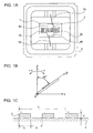
- Figs. 1A to 1C are explanatory views showing an SAW resonator of the invention
- Fig. 1A is a plan view
- Fig. 1B is an explanatory view showing the cut angle of a piezoelectric substrate
- Fig. 1C is a cross-sectional view of an IDT.
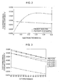
- Fig. 2 is a graph showing the relationship between the electrode thickness H/ ⁇ and the electromechanical coupling coefficient k 2 of the SAW resonator of the invention and of the related art.
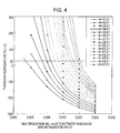
- Fig. 3 is a graph showing the relationship between the cut angle ⁇ and the electromechanical coupling coefficient k 2 , when the electrode thickness H/ ⁇ is set in the range of 0.01 to 0.05.
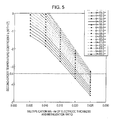
- Fig. 4 is a graph showing the relationship between the multiplication H/ ⁇ mr of the electrode thickness and the metalization ratio, and the turnover temperature Tp, when the cut angle ⁇ of the SAW resonator of the invention is set in the range of -65° ⁇ ⁇ ⁇ -51°.
- Fig. 5 is a graph showing the relationship between the multiplication H/ ⁇ mr of the electrode thickness and the metalization ratio, and a second-order temperature coefficient b, when the cut angle ⁇ is set in the range of -65° ⁇ ⁇ ⁇ -51°.
- Fig. 6 is an explanatory view showing an SAW device using an ST cut quartz substrate according to the related art.
- Fig. 1A is a plan view of an SAW resonator according to the invention.
- the SAW resonator has a structure in which an IDT 2, constructed with positive electrode fingers and nagative electrode fingers that are alternately inserted therein, and grating reflectors 3a and 3b for reflecting a surface acoustic wave by both sides of the IDT 2, on a piezoelectric substrate 1.
- Input/output pads 4a and 4b of the IDT 2 are electrically connected to input/output terminals of a package 6 by metal wires 5a and 5b, and an opening of the package 6 is air-tightly sealed by a lid.
- Fig. 1A is a plan view of an SAW resonator according to the invention.
- the SAW resonator has a structure in which an IDT 2, constructed with positive electrode fingers and nagative electrode fingers that are alternately inserted therein, and grating reflectors 3a and 3b for reflecting a surface acoustic wave by both
- the piezoelectric substrate 1 is a quartz plate in which a cut angle ⁇ of a rotated Y-cut quartz substrate is set to a position that is rotated in counter-clockwise direction by -52° from a crystal Z-axis, and in which a propagation direction of the SAW is set in a Z'-axis direction substantially perpendicular (90° ⁇ 5°) to a crystal X-axis, and an excited SAW is an SH wave.
- the above-described cut angle is represented by an Euler angle (0°, 38°, 90° ⁇ 5°).
- the electrodes of the IDT 2 and the grating reflectors 3a and 3b each are made of Ta or an alloyed metal containing Ta as the main component.
- 1C is a cross-sectional view of the IDT 2.
- the electrode thickness is represented by H/ ⁇ , that is, a value obtained by standardizing the thickness by the wavelength ⁇ .
- a metalization ratio mr is represented by (electrode finger widths L)/ (electrode finger widths L + spaces S between electrode fingers).
- Fig. 2 is a graph showing the comparison of an electromechanical coupling coefficient k 2 between the case, in which a Ta film is formed on the quartz plate in which the cut angle ⁇ in the invention is set in the vicinity of -52° and the propagation direction of the SAW is set substantially perpendicular to the crystal X-axis, and the case, in which an AI film is formed on an ST cut quartz substrate according to the related art. As shown in Fig.
- Fig. 3 is a graph showing the relationship between the cut angle ⁇ and the electromechanical coupling coefficient k 2 , and showing the electromechanical coupling coefficient k 2 when the cut angle ⁇ is set in the range of -65° to -51° and the electrode thickness H/ ⁇ is varied in the range of 0.01 to 0.05.
- the electromechanical coupling coefficient k 2 can be made larger, compared with the case in which an Al film is formed on the ST cut quartz substrate according to the
- the quartz substrate is used in which the cut angle ⁇ is set in the range of -65° ⁇ ⁇ ⁇ -51° and the propagation direction of SAW is set substantially perpendicular to the crystal X-axis, electrodes are composed of Ta films on the quartz substrate, and the H/ ⁇ is set in the range of 0.01 ⁇ H/ ⁇ , preferably, in the range of 0.01 ⁇ H/ ⁇ ⁇ 0.05. Therefore, the electromechanical coupling coefficient k 2 is made larger than that in the related art in which Al film is formed on the ST cut quartz substrate, such that characteristics of a broadband can be achieved when a filter is provided.
- Fig. 4 is a graph showing the relationship between the multiplication H/ ⁇ mr of the electrode thickness and the metalization ratio, and the turnover temperature Tp, obtained by calculation when the cut angle ⁇ is set in the range of -65° ⁇ ⁇ ⁇ -51°.
- Fig. 4 shows that the turnover temperature Tp can be set around room temperature 25°C when the cut angle ⁇ is set in the range of -65° ⁇ ⁇ ⁇ -51° and the multiplication H/ ⁇ •mr of the electrode thickness and the metalization ratio is set in the range of 0.004 ⁇ H/ ⁇ mr ⁇ 0.021.
- the electromechanical coupling coefficient k 2 can be made larger than that in the related art, such that the characteristics of a broadband can be achieved when a filter is provided.
- the cut angle ⁇ is set more than -51°, the turnover temperature Tp cannot be set around room temperature.
- the cut angle ⁇ is set less than -65°, the sensitivity of the turnover temperature Tp with respect to the electrode thickness H/ ⁇ remarkably increases, so that it is very hard to control the turnover temperature. Therefore, it is not proper to set the cut angle ⁇ in the range of ⁇ > -51° and ⁇ ⁇ -65° in terms of practical aspects.
- Fig. 5 is a graph showing the relationship between the multiplication H/ ⁇ mr of the electrode thickness and the metalization ratio, and a second-order temperature coefficient b, obtained by calculation when the cut angle ⁇ of the SAW device according to the invention is set in the range of -65° ⁇ ⁇ ⁇ -51°.
- Fig. 5 is a graph showing the relationship between the multiplication H/ ⁇ mr of the electrode thickness and the metalization ratio, and a second-order temperature coefficient b, obtained by calculation when the cut angle ⁇ of the SAW device according to the invention is set in the range of -65° ⁇ ⁇ ⁇ -51°.
- the turnover temperature can be easily set around room temperature by setting the multiplication H/ ⁇ •mr of the electrode thickness and the metalization ratio in the range of 0.004 ⁇ H/ ⁇ •mr ⁇ 0.021. Further, by setting the multiplication in the range of H/ ⁇ •mr ⁇ 0.019, the second-order temperature coefficient can be made smaller than that in the related art.
- the turnover temperature can be easily set around room temperature, and the second-order temperature coefficient can be made smaller than that in the related art.
- SAW resonator of one port as shown in Fig. 1 has been described.
- SAW devices such as the SAW resonator of two ports, a double mode SAW (DMS) filter using sound combination of the SAW resonator, a ladder type SAW filter in which SAW resonators are disposed in a ladder shape in series and parallel arms, and a transversal SAW filter in which an input IDT and an output IDT are disposed at a predetermined interval.
- DMS double mode SAW
- the materials of the electrodes are not limited thereto, and it is clear that the same effects can be obtained when the electrodes are made of materials heavier than Al such as W, Ag, and Au, or alloyed metals containing the heavier materials.
- the same effects of the invention can be achieved even when a protective film is formed of SiO 2 on the IDT or the grating reflector, or when other metal film is formed on an upper portion of the electrode or on a lower portion of the electrode for the purpose of a contact layer and the improvement of power withstanding performance.
- the SAW device of the invention can be applied to a sensor device, a module device, and an oscillation circuit, etc.
- the SAW device of the invention is used in a voltage control SAW oscillator (VCSO) or the like, the capacity ratio ⁇ can be made small, so that a frequency variable width can be extended.
- VCSO voltage control SAW oscillator
- the SAW device of the invention may have other structures, such as a flip chip bonding (FCB) structure in which an electrode pad of the SAW chip is connected to a terminal of the package with metallic bumps, a CSP (Chip Size Package) structure in which the SAW chip is flip-chip-bonded onto a wiring board and the vicinity of the SAW chip is sealed with resin, a WLCSP (Wafer Level Chip Size Package) structure in which a metal film or a resin layer is provided on the SAW chip so that a package or a wiring substrate is unnecessary, and an AQP (All Quartz Package) structure in which a quartz device is inserted between quartz or glass substrates so as to seal the laminated layer.
- FCB flip chip bonding
- CSP Chip Size Package
- WLCSP Wafer Level Chip Size Package
- AQP All Quartz Package
- the quartz device is simply inserted between quartz or glass substrates, a package is unnecessary and the structure can be made thinner. Further, if using low-fusing-point glass sealing or directly sealing, out gas due to an adhesive is reduced, thereby exhibiting excellent aging characteristics.
Landscapes
- Physics & Mathematics (AREA)
- Acoustics & Sound (AREA)
- Surface Acoustic Wave Elements And Circuit Networks Thereof (AREA)
Abstract
Description
- The present invention relates to a surface acoustic wave device using a quartz substrate and, in particular, to a surface acoustic wave device which can achieve excellent frequency temperature characteristic of a broadband.
- In recent years, a surface acoustic wave (hereinafter, referred to as SAW) device has been widely used in mobile communication terminal or other apparatuses for a vehicle. In particular, a surface acoustic wave device is required to have excellent frequency temperature characteristic of a broadband.
- An SAW device, using an ST cut quartz substrate as an SAW device according to the related art, has been proposed. The ST cut quartz substrate is a cut name of a quartz substrate having a plane (XZ' plane) which is rotated in the counter-clockwise direction from an XZ plane about a crystal X-axis by 42.75° from a crystal Z-axis, and uses an SAW (hereinafter, referred to as "ST cut quartz SAW") that is a (P+SV) wave called a Rayleigh wave which propagates in the crystal X-axis direction. The ST cut quartz SAW device has been widely used for an SAW resonator functioning as an oscillation element, and for an IF filter disposed between an RF stage and an IC of a mobile communication terminal. Fig. 6 is a view showing the configuration of the ST cut quartz SAW resonator, in which a comb-type electrode (hereinafter, referred to as "IDT") 102 having a plurality of electrode fingers alternately inserted therein is disposed on an ST
cut quartz substrate 101, andgrating reflectors grating reflectors - In the ST cut quartz SAW device, a first-order temperature coefficient of the frequency temperature characteristic is zero, and the characteristic is indicated by a second-order curve. When the turnover temperature is set to the middle of the available temperature range, the amount of frequency variation remarkably decreases. Accordingly, it is well known that frequency stability is excellent.
- However, in the above-described ST cut quartz SAW device, even though the first-order temperature coefficient is zero, a second-order temperature coefficient is relatively high -3.4(10-8/°C2). Therefore, if the available temperature range is expanded, a problem occurs in which the amount of frequency variation sharply increases. In addition, since the electromechanical coupling coefficient k2 of the ST cut quartz SAW device is small, it is difficult to achieve characteristics of a broadband when a filter is provided.
- When a piezoelectric substrate having a large electromechanical coupling coefficient k2, like that of Li2B4O7, is used in order to widen the band, the frequency temperature characteristic deteriorate, and the margin should be sufficiently ensured for security standards such as insertion loss in the operation temperature range and attenuation amount in the vicinity of a passing band, such that the manufacturing yield deteriorates.
- In contrary, in Japanese Patent No. 3353742 and in Michio Kadota, "Small-sized resonator IF filter using shear horizontal wave on heavy metal film/quartz substrate", IEEE International Frequency Control Symp. Proc., pp.50 to 54(2002), by using an SH wave which propagates in a direction rotated in a 90° plane with respect to the propagation direction of the ST cut quartz SAW, or by using materials, having a heavier gravity than that of the piezoelectric substrate, such as W, Ta to form electrodes, an electromechanical coupling coefficient larger than that of the ST cut quartz SAW is obtained. Therefore, characteristics of a broadband can be achieved when a filter is provided.
- However, in the SAW device disclosed in Japanese Patent No. 3353742 or in Michio Kadota, "Small-sized resonator IF filter using shear horizontal wave on heavy metal film/quartz substrate", IEEE International Frequency Control Symp. Proc., pp.50 to 54(2002), characteristics of a broadband can be achieved easier than in the ST cut quartz SAW device. On the other hand, a second-order temperature coefficient of the frequency temperature characteristic is substantially equal to that of the ST cut quartz SAW device, and the problem still remains in which the amount of frequency variation sharply increases when the available temperature range is expanded.
- An advantage of some aspects of the invention is that it provides an SAW device which uses a quartz substrate as a piezoelectric substrate and an SH wave and can achieve excellent frequency temperature characteristic of a broadband.
- According to a first aspect of the invention, a surface acoustic wave device includes a piezoelectric substrate and an IDT formed on the piezoelectric substrate and uses an excited wave as an SH wave. In this case, the piezoelectric substrate is a quartz plate in which a cut angle θ of a rotated Y-cut quartz substrate is set in the range of -65° ≤ θ ≤ -51° in a counter-clockwise direction from a crystal Z-axis and the propagation direction of a surface acoustic wave is set in the range (90° ± 5°) with respect to a crystal X-axis. The IDT is made of Ta or an alloyed metal containing Ta as the main component.
- In the surface acoustic wave device, preferably, an electrode thickness H/λ, standardized by a wavelength of the IDT, is set in the range of H/λ ≥ 0.01 when a wavelength of an excited surface acoustic wave is set to be λ.
- Further, in the surface acoustic wave device, preferably, the multiplication H/λ·mr of the electrode thickness H/λ and metalization ratio mr is set in the range of 0.004 ≤ H/λ•mr < 0.019, when a metalization ratio mr of the electrode fingers of the IDT is represented by (electrode finger widths) / (electrode finger widths + spaces between electrode fingers).
- Furthermore, according to a second aspect, a complex device is provide which uses the surface acoustic wave device according to the first aspect and includes an oscillation circuit and a module device.
- According to the first aspect of the invention, a surface acoustic wave device includes a piezoelectric substrate and an IDT formed on the piezoelectric substrate and uses an excited wave as an SH wave. In this case, the piezoelectric substrate is a quartz plate in which a cut angle θ of a rotated Y-cut quartz substrate is set in the range of -65° ≤ θ ≤ -51° in a counter-clockwise direction from a crystal Z-axis and the propagation direction of a surface acoustic wave is set in the range (90° ± 5°) with respect to a crystal X-axis. The IDT is made of Ta or an alloyed metal containing Ta as the main component. Therefore, excellent frequency temperature characteristic of a broadband can be achieved.
- In the surface acoustic wave device, the electrode thickness H/λ, standardized by a wavelength of the IDT, is set in the range of H/λ ≥ 0.01 when the wavelength of the excited surface acoustic wave is set to be λ. Therefore, the electromechanical coupling coefficient k2 can be made larger than that in the related art in which Al film is formed on the ST cut quartz substrate, such that characteristics of a broadband can be achieved.
- Further, in the surface acoustic wave device, the multiplication H/λ·mr of the electrode thickness H/λ and metalization ratio mr is set in the range of 0.004 ≤ H/λ•mr ≤ 0.019, when the metalization ratio mr of the electrode fingers of the IDT is represented by (electrode finger widths) / (electrode finger widths + spaces between electrode fingers). Therefore, a second-order temperature coefficient can be made smaller than that in the related art, and the turnover temperature can be easily set around room temperature.
- Furthermore, according to the second aspect, the surface acoustic wave device is used for a complex device such as an oscillation circuit and a module device. Therefore, a module device or an oscillation with high-performance can be provided.
- The invention will be described with reference to the accompanying drawings, wherein like numbers reference like elements.
- Figs. 1A to 1C are explanatory views showing an SAW resonator of the invention, Fig. 1A is a plan view, Fig. 1B is an explanatory view showing the cut angle of a piezoelectric substrate, and Fig. 1C is a cross-sectional view of an IDT.
- Fig. 2 is a graph showing the relationship between the electrode thickness H/λ and the electromechanical coupling coefficient k2 of the SAW resonator of the invention and of the related art.
- Fig. 3 is a graph showing the relationship between the cut angle θ and the electromechanical coupling coefficient k2, when the electrode thickness H/λ is set in the range of 0.01 to 0.05.
- Fig. 4 is a graph showing the relationship between the multiplication H/λ·mr of the electrode thickness and the metalization ratio, and the turnover temperature Tp, when the cut angle θ of the SAW resonator of the invention is set in the range of -65° ≤ θ ≤ -51°.
- Fig. 5 is a graph showing the relationship between the multiplication H/λ·mr of the electrode thickness and the metalization ratio, and a second-order temperature coefficient b, when the cut angle θ is set in the range of -65° ≤ θ ≤ -51°.
- Fig. 6 is an explanatory view showing an SAW device using an ST cut quartz substrate according to the related art.
- Hereinafter, a preferred embodiment of the invention will be described in detail with reference to the accompanying drawings. Fig. 1A is a plan view of an SAW resonator according to the invention. The SAW resonator has a structure in which an
IDT 2, constructed with positive electrode fingers and nagative electrode fingers that are alternately inserted therein, andgrating reflectors IDT 2, on apiezoelectric substrate 1. Input/output pads IDT 2 are electrically connected to input/output terminals of apackage 6 bymetal wires package 6 is air-tightly sealed by a lid. As shown in Fig. 1B, thepiezoelectric substrate 1 is a quartz plate in which a cut angle θ of a rotated Y-cut quartz substrate is set to a position that is rotated in counter-clockwise direction by -52° from a crystal Z-axis, and in which a propagation direction of the SAW is set in a Z'-axis direction substantially perpendicular (90°±5°) to a crystal X-axis, and an excited SAW is an SH wave. Further, the above-described cut angle is represented by an Euler angle (0°, 38°, 90°±5°). Furthermore, the electrodes of theIDT 2 and thegrating reflectors IDT 2. In an embodiment to be described below, when a wavelength of SAW excited on theIDT 2 is set to be λ, the electrode thickness is represented by H/λ, that is, a value obtained by standardizing the thickness by the wavelength λ. A metalization ratio mr is represented by (electrode finger widths L)/ (electrode finger widths L + spaces S between electrode fingers). - First, the relationship between the electrode thickness H/λ and an electromechanical coupling coefficient k2 in the SAW device according to the invention has been studied. Fig. 2 is a graph showing the comparison of an electromechanical coupling coefficient k2 between the case, in which a Ta film is formed on the quartz plate in which the cut angle θ in the invention is set in the vicinity of -52° and the propagation direction of the SAW is set substantially perpendicular to the crystal X-axis, and the case, in which an AI film is formed on an ST cut quartz substrate according to the related art. As shown in Fig. 2, in the case in which an AI film is formed on the ST cut quartz substrate according to the related art, as the electrode thickness H/λ increases, the electromechanical coupling coefficient k2 monotonically decreases, and the maximum value of k2 is 0.0014 at the most. In contrary, in the invention, as the electrode thickness H/λ increases, K2 sharply increases, so that k2 is larger than that in the related art when H/λ ≥ 0.01.
- Fig. 3 is a graph showing the relationship between the cut angle θ and the electromechanical coupling coefficient k2, and showing the electromechanical coupling coefficient k2 when the cut angle θ is set in the range of -65° to -51° and the electrode thickness H/λ is varied in the range of 0.01 to 0.05. As shown in Fig. 3, by setting the cut angle θ in the range of -65° ≤ θ ≤ -51° and the electrode thickness H/λ in the range of 0.01 ≤ H/λ ≤ 0.05, the electromechanical coupling coefficient k2 can be made larger, compared with the case in which an Al film is formed on the ST cut quartz substrate according to the
- As described above, the quartz substrate is used in which the cut angle θ is set in the range of -65° ≤ θ ≤ -51° and the propagation direction of SAW is set substantially perpendicular to the crystal X-axis, electrodes are composed of Ta films on the quartz substrate, and the H/λ is set in the range of 0.01 ≤ H/λ, preferably, in the range of 0.01 ≤ H/λ ≤ 0.05. Therefore, the electromechanical coupling coefficient k2 is made larger than that in the related art in which Al film is formed on the ST cut quartz substrate, such that characteristics of a broadband can be achieved when a filter is provided.
- Next, the frequency temperature characteristic of the SAW device of the invention has been studied. Fig. 4 is a graph showing the relationship between the multiplication H/λ·mr of the electrode thickness and the metalization ratio, and the turnover temperature Tp, obtained by calculation when the cut angle θ is set in the range of -65° ≤ θ ≤ -51°. Fig. 4 shows that the turnover temperature Tp can be set around
room temperature 25°C when the cut angle θ is set in the range of -65° ≤ θ ≤ -51° and the multiplication H/λ•mr of the electrode thickness and the metalization ratio is set in the range of 0.004 ≤ H/λ·mr ≤ 0.021. Here, when the electrode thickness H/λ is set in the range of H/λ ≥ 0.01, the electromechanical coupling coefficient k2 can be made larger than that in the related art, such that the characteristics of a broadband can be achieved when a filter is provided. When the cut angle θ is set more than -51°, the turnover temperature Tp cannot be set around room temperature. On the other hand, when the cut angle θ is set less than -65°, the sensitivity of the turnover temperature Tp with respect to the electrode thickness H/λ remarkably increases, so that it is very hard to control the turnover temperature. Therefore, it is not proper to set the cut angle θ in the range of θ > -51° and θ < -65° in terms of practical aspects. - Fig. 5 is a graph showing the relationship between the multiplication H/λ·mr of the electrode thickness and the metalization ratio, and a second-order temperature coefficient b, obtained by calculation when the cut angle θ of the SAW device according to the invention is set in the range of -65° ≤ θ ≤ -51°. In Fig. 5, when the cut angle θ is set in the range of -65° ≤ θ ≤ -51°, by setting the multiplication H/λ·mr of the electrode thickness and the metalization ratio in the range of H/λ·mr < 0.019, the second-order temperature coefficient b can be set less than the second-order temperature coefficient b = -3.4(10-8/°C2) of the ST cut quartz device according to the related art or the SAW device disclosed in Japanese Patent No. 3353742 or in Michio Kadota, "Small-sized resonator IF filter using shear horizontal wave on heavy metal film/quartz substrate", IEEE International Frequency Control Symp. Proc., pp.50 to 54(2002).
- As described above, in the SAW device in which the electrodes are formed of Ta films on a rotated Y-cut quartz substrate in which the
cut angle 0 is set in the range of -65° ≤ θ ≤ -51° and the propagation direction of the SAW is rotated by about 90° with respect to the crystal X-axis, the turnover temperature can be easily set around room temperature by setting the multiplication H/λ•mr of the electrode thickness and the metalization ratio in the range of 0.004 ≤ H/λ•mr ≤ 0.021. Further, by setting the multiplication in the range of H/λ•mr < 0.019, the second-order temperature coefficient can be made smaller than that in the related art. Furthermore, when the multiplication H/λ•mr of the electrode thickness and the metalization ratio is set in the range of 0.004 ≤ H/λ•mr < 0.019, the turnover temperature can be easily set around room temperature, and the second-order temperature coefficient can be made smaller than that in the related art. - Hereinabove, only the SAW resonator of one port as shown in Fig. 1 has been described. However, the same effects can be obtained when the invention is applied to various types of SAW devices such as the SAW resonator of two ports, a double mode SAW (DMS) filter using sound combination of the SAW resonator, a ladder type SAW filter in which SAW resonators are disposed in a ladder shape in series and parallel arms, and a transversal SAW filter in which an input IDT and an output IDT are disposed at a predetermined interval.
- Further, even though the electrodes each have been made of Ta or an alloyed metal containing Ta as the main component, the materials of the electrodes are not limited thereto, and it is clear that the same effects can be obtained when the electrodes are made of materials heavier than Al such as W, Ag, and Au, or alloyed metals containing the heavier materials.
- Furthermore, in the above-described SAW device, it is clear that the same effects of the invention can be achieved even when a protective film is formed of SiO2 on the IDT or the grating reflector, or when other metal film is formed on an upper portion of the electrode or on a lower portion of the electrode for the purpose of a contact layer and the improvement of power withstanding performance. Further, the SAW device of the invention can be applied to a sensor device, a module device, and an oscillation circuit, etc. Furthermore, when the SAW device of the invention is used in a voltage control SAW oscillator (VCSO) or the like, the capacity ratio γ can be made small, so that a frequency variable width can be extended.
- Besides the structure in which the SAW chip is wire-boned to the package, as shown in Fig. 1, the SAW device of the invention may have other structures, such as a flip chip bonding (FCB) structure in which an electrode pad of the SAW chip is connected to a terminal of the package with metallic bumps, a CSP (Chip Size Package) structure in which the SAW chip is flip-chip-bonded onto a wiring board and the vicinity of the SAW chip is sealed with resin, a WLCSP (Wafer Level Chip Size Package) structure in which a metal film or a resin layer is provided on the SAW chip so that a package or a wiring substrate is unnecessary, and an AQP (All Quartz Package) structure in which a quartz device is inserted between quartz or glass substrates so as to seal the laminated layer. In the AQP structure, since the quartz device is simply inserted between quartz or glass substrates, a package is unnecessary and the structure can be made thinner. Further, if using low-fusing-point glass sealing or directly sealing, out gas due to an adhesive is reduced, thereby exhibiting excellent aging characteristics.
- The entire disclosure of Japanese Patent Application No. 2005-001052, filed January 6, 2005 is expressly incorporated by reference herein.
Claims (4)
- A surface acoustic wave device having a piezoelectric substrate and an IDT formed on the piezoelectric substrate and using an excited wave as an SH wave,
wherein the piezoelectric substrate is a quartz plate in which a cut angle θ of a rotated Y-cut quartz substrate is set in the range of -65° ≤ θ ≤ -51° in a counter-clockwise direction from a crystal Z-axis and the propagation direction of a surface acoustic wave is set in the range (90° ± 5°) with respect to a crystal X-axis, and
the IDT is made of Ta or an alloyed metal containing Ta as the main component. - The surface acoustic wave device according to Claim 1,
wherein an electrode thickness H/λ, standardized by a wavelength of the IDT, is set in the range of H/λ ≥ 0.01 when a wavelength of an excited surface acoustic wave is set to be λ. - The surface acoustic wave device according to Claim 2,
wherein the multiplication H/λ•mr of the electrode thickness H/λ and metalization ratio mr is set in the range of 0.004 ≤ H/λ•mr < 0.019, when a metalization ratio mr of the electrode fingers of the IDT is represented by (electrode finger widths) / (electrode finger widths + spaces between electrode fingers). - A complex device using the surface acoustic wave device as described in Claim 1, 2 or 3 and including an oscillation circuit and a module device.
Applications Claiming Priority (1)
| Application Number | Priority Date | Filing Date | Title |
|---|---|---|---|
| JP2005001052A JP4148220B2 (en) | 2005-01-06 | 2005-01-06 | Surface acoustic wave device, composite device, oscillation circuit and module |
Publications (2)
| Publication Number | Publication Date |
|---|---|
| EP1679794A2 true EP1679794A2 (en) | 2006-07-12 |
| EP1679794A3 EP1679794A3 (en) | 2007-07-04 |
Family
ID=36095659
Family Applications (1)
| Application Number | Title | Priority Date | Filing Date |
|---|---|---|---|
| EP06000174A Withdrawn EP1679794A3 (en) | 2005-01-06 | 2006-01-05 | Surface acoustic wave device |
Country Status (3)
| Country | Link |
|---|---|
| US (1) | US7463119B2 (en) |
| EP (1) | EP1679794A3 (en) |
| JP (1) | JP4148220B2 (en) |
Cited By (1)
| Publication number | Priority date | Publication date | Assignee | Title |
|---|---|---|---|---|
| DE102014105860A1 (en) | 2014-04-25 | 2015-10-29 | Epcos Ag | Electroacoustic component and crystal sections for electroacoustic components |
Families Citing this family (5)
| Publication number | Priority date | Publication date | Assignee | Title |
|---|---|---|---|---|
| CN103929147B (en) * | 2013-01-11 | 2017-02-01 | 中国科学院声学研究所 | Single-ended pair SAW resonator with high quality factors |
| WO2018051800A1 (en) * | 2016-09-16 | 2018-03-22 | 株式会社大真空 | Piezoelectric vibration device |
| US9970993B1 (en) * | 2017-02-16 | 2018-05-15 | Ford Global Technologies, Llc | Sensor system for measuring battery internal state |
| CN116888891A (en) * | 2021-04-20 | 2023-10-13 | 株式会社村田制作所 | Resonator |
| CN118266168A (en) * | 2022-01-19 | 2024-06-28 | 株式会社村田制作所 | Crystal resonator |
Citations (3)
| Publication number | Priority date | Publication date | Assignee | Title |
|---|---|---|---|---|
| USRE35204E (en) * | 1977-01-24 | 1996-04-09 | The Secretary Of State For Defence In Her Britannic Majesty's Government Of The United Kingdom Of Great Britain And Northern Ireland | Acoustic wave devices employing surface skimming bulk waves |
| JP3353742B2 (en) | 1999-05-07 | 2002-12-03 | 株式会社村田製作所 | Surface wave resonator, surface wave device, communication device |
| JP2005001052A (en) | 2003-06-11 | 2005-01-06 | National Institute Of Information & Communication Technology | Method for autonomous movement control of artificial object by recognition of human intention, communication system and program thereof |
Family Cites Families (11)
| Publication number | Priority date | Publication date | Assignee | Title |
|---|---|---|---|---|
| JPS5545284A (en) | 1978-09-27 | 1980-03-29 | Toyo Commun Equip Co Ltd | Slip wave crystal vibration device |
| JPS5833309A (en) | 1981-08-21 | 1983-02-26 | Toyo Commun Equip Co Ltd | Slip wave resonator |
| JP3255502B2 (en) | 1993-07-26 | 2002-02-12 | 東洋通信機株式会社 | Highly stable surface acoustic wave device |
| US6172582B1 (en) * | 1996-02-20 | 2001-01-09 | Cts Corporation | Saw resonator and ladder filter with specified number of reflector electrode fingers |
| JP3339350B2 (en) * | 1997-02-20 | 2002-10-28 | 株式会社村田製作所 | Surface acoustic wave device |
| JP3301399B2 (en) * | 1998-02-16 | 2002-07-15 | 株式会社村田製作所 | Surface acoustic wave device |
| JP3317273B2 (en) * | 1998-08-25 | 2002-08-26 | 株式会社村田製作所 | Surface wave resonators, filters, duplexers, communication equipment |
| JP3435638B2 (en) * | 2000-10-27 | 2003-08-11 | 株式会社村田製作所 | Surface acoustic wave device and method of manufacturing the same |
| JP2004040636A (en) * | 2002-07-05 | 2004-02-05 | Murata Mfg Co Ltd | Surface wave device |
| JP2004007846A (en) | 2003-09-08 | 2004-01-08 | Murata Mfg Co Ltd | Surface wave resonator |
| EP1732216B1 (en) | 2004-04-01 | 2014-01-08 | Seiko Epson Corporation | Surface acoustic device |
-
2005
- 2005-01-06 JP JP2005001052A patent/JP4148220B2/en not_active Expired - Fee Related
- 2005-12-29 US US11/319,404 patent/US7463119B2/en not_active Expired - Fee Related
-
2006
- 2006-01-05 EP EP06000174A patent/EP1679794A3/en not_active Withdrawn
Patent Citations (3)
| Publication number | Priority date | Publication date | Assignee | Title |
|---|---|---|---|---|
| USRE35204E (en) * | 1977-01-24 | 1996-04-09 | The Secretary Of State For Defence In Her Britannic Majesty's Government Of The United Kingdom Of Great Britain And Northern Ireland | Acoustic wave devices employing surface skimming bulk waves |
| JP3353742B2 (en) | 1999-05-07 | 2002-12-03 | 株式会社村田製作所 | Surface wave resonator, surface wave device, communication device |
| JP2005001052A (en) | 2003-06-11 | 2005-01-06 | National Institute Of Information & Communication Technology | Method for autonomous movement control of artificial object by recognition of human intention, communication system and program thereof |
Non-Patent Citations (2)
| Title |
|---|
| KADOTA ET AL: "Small-Sized Resonator IF Filter Using Shear Horizontal Wave on Heavy Metal Film/Quartz Substrate", 2002 IEEE INTERNATIONAL FREQUENCY CONTROL SYMPOSIUM AND PDA EXHIBITION, 29 May 2002 (2002-05-29), pages 50 - 54, XP010618918 * |
| MICHIO KADOTA: "Small-sized resonator IF filter using shear horizontal wave on heavy metal film/quartz substrate", IEEE INTERNATIONAL FREQUENCY CONTROL SYMP. PROC., 2002, pages 50 - 54 |
Cited By (2)
| Publication number | Priority date | Publication date | Assignee | Title |
|---|---|---|---|---|
| DE102014105860A1 (en) | 2014-04-25 | 2015-10-29 | Epcos Ag | Electroacoustic component and crystal sections for electroacoustic components |
| US10333488B2 (en) | 2014-04-25 | 2019-06-25 | Snaptrack, Inc. | Electroacoustic component and crystal cuts for electroacoustic components |
Also Published As
| Publication number | Publication date |
|---|---|
| US7463119B2 (en) | 2008-12-09 |
| US20060145569A1 (en) | 2006-07-06 |
| JP2006191330A (en) | 2006-07-20 |
| JP4148220B2 (en) | 2008-09-10 |
| EP1679794A3 (en) | 2007-07-04 |
Similar Documents
| Publication | Publication Date | Title |
|---|---|---|
| JP7433268B2 (en) | Elastic wave devices, duplexers and communication devices | |
| US7589451B2 (en) | Surface acoustic wave device | |
| US8084917B2 (en) | Surface acoustic wave resonator, surface acoustic wave oscillator, and surface acoustic wave module device | |
| US7382217B2 (en) | Surface acoustic wave device | |
| JP2006203408A (en) | Surface acoustic wave device | |
| WO2007094368A1 (en) | Surface acoustic wave device, surface acoustic wave filter employing same and antenna duplexer, and electronic apparatus employing same | |
| US8692439B2 (en) | Surface acoustic wave resonator, surface acoustic wave oscillator, and electronic device | |
| CN101379700B (en) | Surface acoustic wave device, and manufacturing method thereof | |
| US7453335B2 (en) | Surface acoustic wave resonator, surface acoustic wave filter and surface acoustic wave duplexer, and communications equipment | |
| US7750533B2 (en) | Surface acoustic wave (SAW) device, module and oscillator for improving a Q factor | |
| US7463119B2 (en) | Surface acoustic wave device | |
| CN100539411C (en) | Surface acoustic wave device | |
| JP4356773B2 (en) | Surface acoustic wave device and module device or oscillation circuit using the same | |
| JP2010245722A (en) | Surface acoustic wave element and surface acoustic wave device using the same | |
| JP2010103720A (en) | Surface acoustic wave device | |
| JP4356675B2 (en) | Surface acoustic wave device | |
| JP4148216B2 (en) | Surface acoustic wave device and module device or oscillation circuit using the same | |
| US20250105820A1 (en) | Bragg stack structure for spurious mode suppression in solidly-mounted acoustic resonator | |
| JP3412621B2 (en) | Surface acoustic wave device | |
| US20250141428A1 (en) | Resonator with complementarily oriented piezoelectric structure | |
| JP2007019976A (en) | Vertically coupled multimode SAW filter, module device | |
| JP2007019975A (en) | Surface acoustic wave device, module device, oscillation circuit | |
| JP2007013682A (en) | Surface acoustic wave device | |
| WO2025090719A1 (en) | Resonator having a complementarily oriented piezoelectric structure | |
| JP2007325084A (en) | Surface acoustic wave element and surface acoustic wave device |
Legal Events
| Date | Code | Title | Description |
|---|---|---|---|
| PUAI | Public reference made under article 153(3) epc to a published international application that has entered the european phase |
Free format text: ORIGINAL CODE: 0009012 |
|
| AK | Designated contracting states |
Kind code of ref document: A2 Designated state(s): AT BE BG CH CY CZ DE DK EE ES FI FR GB GR HU IE IS IT LI LT LU LV MC NL PL PT RO SE SI SK TR |
|
| AX | Request for extension of the european patent |
Extension state: AL BA HR MK YU |
|
| PUAL | Search report despatched |
Free format text: ORIGINAL CODE: 0009013 |
|
| AK | Designated contracting states |
Kind code of ref document: A3 Designated state(s): AT BE BG CH CY CZ DE DK EE ES FI FR GB GR HU IE IS IT LI LT LU LV MC NL PL PT RO SE SI SK TR |
|
| AX | Request for extension of the european patent |
Extension state: AL BA HR MK YU |
|
| 17P | Request for examination filed |
Effective date: 20070906 |
|
| 17Q | First examination report despatched |
Effective date: 20071010 |
|
| AKX | Designation fees paid |
Designated state(s): DE FR GB |
|
| RAP1 | Party data changed (applicant data changed or rights of an application transferred) |
Owner name: SEIKO EPSON CORPORATION |
|
| STAA | Information on the status of an ep patent application or granted ep patent |
Free format text: STATUS: THE APPLICATION IS DEEMED TO BE WITHDRAWN |
|
| 18D | Application deemed to be withdrawn |
Effective date: 20120112 |